EP3627681A1 - Alimentation à découpage avec une inductance seule et plusieurs sorties - Google Patents
Alimentation à découpage avec une inductance seule et plusieurs sorties Download PDFInfo
- Publication number
- EP3627681A1 EP3627681A1 EP18000746.0A EP18000746A EP3627681A1 EP 3627681 A1 EP3627681 A1 EP 3627681A1 EP 18000746 A EP18000746 A EP 18000746A EP 3627681 A1 EP3627681 A1 EP 3627681A1
- Authority
- EP
- European Patent Office
- Prior art keywords
- output
- power supply
- output circuit
- converter
- inductive
- Prior art date
- Legal status (The legal status is an assumption and is not a legal conclusion. Google has not performed a legal analysis and makes no representation as to the accuracy of the status listed.)
- Withdrawn
Links
Images

Classifications
-
- H—ELECTRICITY
- H02—GENERATION; CONVERSION OR DISTRIBUTION OF ELECTRIC POWER
- H02M—APPARATUS FOR CONVERSION BETWEEN AC AND AC, BETWEEN AC AND DC, OR BETWEEN DC AND DC, AND FOR USE WITH MAINS OR SIMILAR POWER SUPPLY SYSTEMS; CONVERSION OF DC OR AC INPUT POWER INTO SURGE OUTPUT POWER; CONTROL OR REGULATION THEREOF
- H02M3/00—Conversion of dc power input into dc power output
- H02M3/02—Conversion of dc power input into dc power output without intermediate conversion into ac
- H02M3/04—Conversion of dc power input into dc power output without intermediate conversion into ac by static converters
- H02M3/10—Conversion of dc power input into dc power output without intermediate conversion into ac by static converters using discharge tubes with control electrode or semiconductor devices with control electrode
- H02M3/145—Conversion of dc power input into dc power output without intermediate conversion into ac by static converters using discharge tubes with control electrode or semiconductor devices with control electrode using devices of a triode or transistor type requiring continuous application of a control signal
- H02M3/155—Conversion of dc power input into dc power output without intermediate conversion into ac by static converters using discharge tubes with control electrode or semiconductor devices with control electrode using devices of a triode or transistor type requiring continuous application of a control signal using semiconductor devices only
- H02M3/156—Conversion of dc power input into dc power output without intermediate conversion into ac by static converters using discharge tubes with control electrode or semiconductor devices with control electrode using devices of a triode or transistor type requiring continuous application of a control signal using semiconductor devices only with automatic control of output voltage or current, e.g. switching regulators
- H02M3/158—Conversion of dc power input into dc power output without intermediate conversion into ac by static converters using discharge tubes with control electrode or semiconductor devices with control electrode using devices of a triode or transistor type requiring continuous application of a control signal using semiconductor devices only with automatic control of output voltage or current, e.g. switching regulators including plural semiconductor devices as final control devices for a single load
-
- H—ELECTRICITY
- H02—GENERATION; CONVERSION OR DISTRIBUTION OF ELECTRIC POWER
- H02M—APPARATUS FOR CONVERSION BETWEEN AC AND AC, BETWEEN AC AND DC, OR BETWEEN DC AND DC, AND FOR USE WITH MAINS OR SIMILAR POWER SUPPLY SYSTEMS; CONVERSION OF DC OR AC INPUT POWER INTO SURGE OUTPUT POWER; CONTROL OR REGULATION THEREOF
- H02M3/00—Conversion of dc power input into dc power output
- H02M3/22—Conversion of dc power input into dc power output with intermediate conversion into ac
- H02M3/24—Conversion of dc power input into dc power output with intermediate conversion into ac by static converters
- H02M3/28—Conversion of dc power input into dc power output with intermediate conversion into ac by static converters using discharge tubes with control electrode or semiconductor devices with control electrode to produce the intermediate ac
- H02M3/325—Conversion of dc power input into dc power output with intermediate conversion into ac by static converters using discharge tubes with control electrode or semiconductor devices with control electrode to produce the intermediate ac using devices of a triode or a transistor type requiring continuous application of a control signal
- H02M3/335—Conversion of dc power input into dc power output with intermediate conversion into ac by static converters using discharge tubes with control electrode or semiconductor devices with control electrode to produce the intermediate ac using devices of a triode or a transistor type requiring continuous application of a control signal using semiconductor devices only
- H02M3/33561—Conversion of dc power input into dc power output with intermediate conversion into ac by static converters using discharge tubes with control electrode or semiconductor devices with control electrode to produce the intermediate ac using devices of a triode or a transistor type requiring continuous application of a control signal using semiconductor devices only having more than one ouput with independent control
-
- H—ELECTRICITY
- H02—GENERATION; CONVERSION OR DISTRIBUTION OF ELECTRIC POWER
- H02M—APPARATUS FOR CONVERSION BETWEEN AC AND AC, BETWEEN AC AND DC, OR BETWEEN DC AND DC, AND FOR USE WITH MAINS OR SIMILAR POWER SUPPLY SYSTEMS; CONVERSION OF DC OR AC INPUT POWER INTO SURGE OUTPUT POWER; CONTROL OR REGULATION THEREOF
- H02M1/00—Details of apparatus for conversion
- H02M1/0045—Converters combining the concepts of switch-mode regulation and linear regulation, e.g. linear pre-regulator to switching converter, linear and switching converter in parallel, same converter or same transistor operating either in linear or switching mode
-
- H—ELECTRICITY
- H02—GENERATION; CONVERSION OR DISTRIBUTION OF ELECTRIC POWER
- H02M—APPARATUS FOR CONVERSION BETWEEN AC AND AC, BETWEEN AC AND DC, OR BETWEEN DC AND DC, AND FOR USE WITH MAINS OR SIMILAR POWER SUPPLY SYSTEMS; CONVERSION OF DC OR AC INPUT POWER INTO SURGE OUTPUT POWER; CONTROL OR REGULATION THEREOF
- H02M1/00—Details of apparatus for conversion
- H02M1/0083—Converters characterised by their input or output configuration
- H02M1/009—Converters characterised by their input or output configuration having two or more independently controlled outputs
Definitions
- the present invention relates to an inductive switching power supply for generating a plurality of regulated output voltages.
- the principle of an inductive switching power supply is based on charging a winding by applying a supply voltage, then switching off the supply voltage supply and then supplying the impressed current to the output voltage.
- Conventional inductive switching power supplies deliver one output voltage per winding.
- the DE 102 18 456 A1 discloses a multiple winding switch mode power supply to provide multiple different output voltages.
- the inductive switched-mode power supply of the invention has a switching, inductive DC / DC converter with an input via which a supply voltage can be supplied and an output for providing an intermediate voltage; a first output circuit with an input connected to the output of the DC / DC converter and an output for providing an output voltage; and at least one further output circuit which has an input connected to the output of the DC / DC converter and an output for providing an output voltage which is different from the output voltage of the first output circuit.
- the switching power supply according to the invention can be used with only one winding several different, regulated output voltages are provided.
- dispensing with additional windings or inductors a simple and inexpensive construction of the inductive switching power supply is made possible.
- the inductive switching power supply according to the invention is that the plurality of output voltages can be regulated individually by the individual output circuits.
- the individual output circuits provide greater flexibility, since by changing one or more output circuits and / or by adding further output circuits, the voltage levels and the number of output voltages provided by the switching power supply can be changed in a simple manner without the converter and / or the basic circuit structure of the Need to modify switching power supply.
- the individual output circuits also only require a smaller variety of switching power supplies for different applications.
- Another advantage of the inductive switched-mode power supply according to the invention is that output voltages can also be provided with only one winding, so that a downstream linear regulator can be dispensed with or the voltage to be bridged by a downstream linear regulator can be reduced.
- the required cooling measures can be reduced, as a result of which the required cooling area can be reduced and standby losses can be reduced, which leads to a space-saving and inexpensive construction of the switching power supply.
- the lower power consumption in the downstream linear controller results in a lower current drop for charging the output capacities, so that it can move closer to the switch-off threshold and the available output power is slightly increased.
- the at least one further output circuit has a switching element between its input and its output, preferably in the form of a transistor, for the optional connection of the further output circuit.
- the at least one further output circuit preferably also has a driver, preferably in the form of a gate driver, for actuating the switching element.
- the at least one further output circuit can be used this embodiment also have a diode between its input and its switching element, so that negative voltages on the switching elements can be avoided when connecting a plurality of output voltages.
- the first output circuit has a diode between its input and its output in order to ensure that the current freewheels.
- the first output circuit can also have a switching element for selectively connecting the first output circuit in a manner analogous to the at least one further output circuit.
- the output circuits are preferably each equipped with a voltage divider.
- the first output circuit and the at least one further output circuit each have a capacitor for setting the voltage level of the output voltage, the capacitances of the capacitors of the first and the at least one further output circuit being different from one another.
- the switching, inductive DC / DC converter of the switching power supply according to the invention is not restricted to any special topology.
- a DC / DC converter in a step-down converter topology, a DC / DC converter in a step-up converter topology or a DC / DC converter in a flyback topology is preferably used.
- the output of the first output circuit and / or the at least one further output circuit can be followed by a linear regulator, with which the respective output voltage can be further reduced.
- a controller for actuating the switching element or its driver, the controller being designed to effect a switching operation of the switching element in the region of a current zero crossing. Switching losses can be reduced in this way.
- a controller for actuating the switching element or its driver, the controller being designed to cause a hysteresis when changing between the output voltages of the first and the at least one further output circuit. In this way Too frequent switching or even linear operation of the switching elements can be avoided.
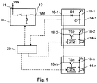
- Fig. 1 the parts of a first embodiment of an inductive switching power supply relevant to the invention are illustrated.
- the inductive switching power supply has a switching, inductive DC / DC converter 10 in a buck converter topology.
- a supply voltage VIN which is, for example, a rectified mains voltage, is fed to an input 11 of the DC / DC converter 10.
- the corresponding AC / DC converter of the switching power supply is in Fig. 1 not shown.
- the DC / DC converter 10 provides an intermediate voltage VM at its output 12.
- the inductive switching power supply also has a first output circuit 14-1, the input 16-1 of which is connected to the output 12 of the DC / DC converter 10 and an output voltage V1 is provided at the output 18-1.
- the output 18-1 is only connected to the input 16-1 via a diode D1 in order to ensure that the current is freewheeling.
- the first output circuit 14-1 has a capacitor C1 for setting the output voltage V1.
- the output voltage V1 of the first output circuit 14-1 is the output voltage of the switching power supply with the highest voltage level.
- the inductive switching power supply also has one or more further output circuits 14-2 ... 14-n.
- the number of these further output circuits 14-2 ... 14-n is basically arbitrary.
- the inputs 16-2 ... 16-n of the further output circuits 14-2 ... 14-n are also each connected to the output 12 of the DC / DC converter 10.
- an output voltage V2 ... Vn is provided, the voltage level of which is set via a capacitor C2 ... Cn. Since the capacitances of the capacitors C1 ... Cn of all output circuits 14-1 ... 14-n are different from one another, the voltage levels of the output voltages V1 ... Vn of the output circuits 14-1 ... 14-n are also different from one another.
- the voltage level of the output voltage V1 of the first output circuit 14-1 is, for example, +15 V and the voltage level of the output voltage V2 of a further output circuit 14-2 is, for example, +5 V.
- the further output circuit 14-2 can then optionally be a preferred one only a single-stage linear regulator must be connected in order to lower the voltage level to +3.3 V, for example.
- the further output circuits 14-2 ... 14-n also each have a switching element TS2 ... TSn in the form of a transistor between their input 16-2 ... 16-n and their output 18-2 ... 18-n .
- the switching elements TS2 ... TSn are each operated by a driver GT2 ... GTn in the form of a gate driver.
- the switching power supply also has a controller 20.
- This controller 20 controls the DC / DC converter 10, in particular its switching element, in order to regulate the intermediate voltage VM.
- the controller 20 controls the drivers GT2 ... GTn of the further output circuits 14-2 ... 14-n in order to actuate their switching elements TS2 ... TSn.
- the controller 20 can also be given feedback about the output voltage V1 of the first output circuit 14-1 in order to regulate the intermediate voltage VM.
- the controller 20 can also be given feedback about the output voltage V2 ... Vn of one or more further output circuits 14-2 ... 14-n.
- these can for example be from the levels of the several output voltages can be combined analogously or digitally combined as an OR connection of the results of the voltage threshold tests.
- these can optionally be connected to the input 16 via a diode (not shown) -2 ... 16-n of the further output circuit 14-2 ... 14-n can be connected.
- the output voltages V2 ... Vn of the further output circuits 14-2 ... 14-n are usually regulated at their voltage levels.
- a hysteresis in the voltage control can be useful. Such a hysteresis can also be used to set the compromise between control accuracy and switching losses.
- controller 20 regulates the switched-mode power supply exclusively to the maximum output voltage level V1 of the first output circuit 14-1, then it may be expedient to separate the output 18-1 from the DC / DC converter 10 via the diode D1 at least partially canceled by a parallel resistor (not shown).
- the additional resistor thus acts as a base load, which limits the maximum switch-off time of the switching power supply and already supplies a smaller output voltage V2 ... Vn to be recharged.
- Fig. 2 shows the parts of a second embodiment of an inductive switching power supply relevant to the invention.
- the switching power supply from Fig. 2 differs from that of the first exemplary embodiment in that the switching, inductive DC / DC converter 10 ′ is configured in a step-up converter topology. Otherwise, the switching power supply corresponds to Fig. 2 and its operation as that of the first embodiment of Fig. 1 .
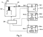
- Fig. 3 shows the parts of a third embodiment of an inductive switching power supply relevant to the invention.
- the switching power supply from Fig. 3 differs from that of the first exemplary embodiment in that the switching, inductive DC / DC converter 10 ′′ is designed in a flyback topology. Otherwise, the switching power supply corresponds to FIG Fig. 3 and its mode of operation also corresponds to that of the first exemplary embodiment of Fig. 1 .
Landscapes
- Engineering & Computer Science (AREA)
- Power Engineering (AREA)
- Dc-Dc Converters (AREA)
Priority Applications (1)
| Application Number | Priority Date | Filing Date | Title |
|---|---|---|---|
| EP18000746.0A EP3627681A1 (fr) | 2018-09-19 | 2018-09-19 | Alimentation à découpage avec une inductance seule et plusieurs sorties |
Applications Claiming Priority (1)
| Application Number | Priority Date | Filing Date | Title |
|---|---|---|---|
| EP18000746.0A EP3627681A1 (fr) | 2018-09-19 | 2018-09-19 | Alimentation à découpage avec une inductance seule et plusieurs sorties |
Publications (1)
| Publication Number | Publication Date |
|---|---|
| EP3627681A1 true EP3627681A1 (fr) | 2020-03-25 |
Family
ID=63667671
Family Applications (1)
| Application Number | Title | Priority Date | Filing Date |
|---|---|---|---|
| EP18000746.0A Withdrawn EP3627681A1 (fr) | 2018-09-19 | 2018-09-19 | Alimentation à découpage avec une inductance seule et plusieurs sorties |
Country Status (1)
| Country | Link |
|---|---|
| EP (1) | EP3627681A1 (fr) |
Cited By (3)
| Publication number | Priority date | Publication date | Assignee | Title |
|---|---|---|---|---|
| CN111769751A (zh) * | 2020-05-15 | 2020-10-13 | 海信(山东)空调有限公司 | 一种直流电源电路及空调器 |
| CN113098265A (zh) * | 2021-04-13 | 2021-07-09 | 苏州力生美半导体有限公司 | 单电感双输出buck开关电源及其充放电控制方法 |
| CN117240087A (zh) * | 2023-11-14 | 2023-12-15 | 苏州越禾泰普数据科技有限公司 | 单输入多输出的直流转直流电路的控制方法、装置及系统 |
Citations (6)
| Publication number | Priority date | Publication date | Assignee | Title |
|---|---|---|---|---|
| US5617015A (en) * | 1995-06-07 | 1997-04-01 | Linear Technology Corporation | Multiple output regulator with time sequencing |
| US6549432B1 (en) * | 2002-02-28 | 2003-04-15 | Koninklijke Philips Electronics N.V. | Single-winding, multiple-output, bi-directional flyback converter |
| DE10218456A1 (de) | 2002-04-25 | 2003-11-06 | Abb Patent Gmbh | Schaltnetzteilanordnung |
| DE10259353A1 (de) * | 2002-12-18 | 2004-07-22 | Infineon Technologies Ag | Verfahren, Schaltungsanordnung und Schaltregler-Kontrollbaustein zur Erzeugung einer Mehrzahl von geregelten Gleichspannungen |
| EP1465329A2 (fr) * | 2003-04-01 | 2004-10-06 | Matsushita Electric Industrial Co., Ltd. | Convertisseur continu-continu à sorties multiples |
| DE102009000395A1 (de) * | 2009-01-23 | 2010-07-29 | Robert Bosch Gmbh | Mehrfach-Schaltregler |
-
2018
- 2018-09-19 EP EP18000746.0A patent/EP3627681A1/fr not_active Withdrawn
Patent Citations (6)
| Publication number | Priority date | Publication date | Assignee | Title |
|---|---|---|---|---|
| US5617015A (en) * | 1995-06-07 | 1997-04-01 | Linear Technology Corporation | Multiple output regulator with time sequencing |
| US6549432B1 (en) * | 2002-02-28 | 2003-04-15 | Koninklijke Philips Electronics N.V. | Single-winding, multiple-output, bi-directional flyback converter |
| DE10218456A1 (de) | 2002-04-25 | 2003-11-06 | Abb Patent Gmbh | Schaltnetzteilanordnung |
| DE10259353A1 (de) * | 2002-12-18 | 2004-07-22 | Infineon Technologies Ag | Verfahren, Schaltungsanordnung und Schaltregler-Kontrollbaustein zur Erzeugung einer Mehrzahl von geregelten Gleichspannungen |
| EP1465329A2 (fr) * | 2003-04-01 | 2004-10-06 | Matsushita Electric Industrial Co., Ltd. | Convertisseur continu-continu à sorties multiples |
| DE102009000395A1 (de) * | 2009-01-23 | 2010-07-29 | Robert Bosch Gmbh | Mehrfach-Schaltregler |
Cited By (4)
| Publication number | Priority date | Publication date | Assignee | Title |
|---|---|---|---|---|
| CN111769751A (zh) * | 2020-05-15 | 2020-10-13 | 海信(山东)空调有限公司 | 一种直流电源电路及空调器 |
| CN113098265A (zh) * | 2021-04-13 | 2021-07-09 | 苏州力生美半导体有限公司 | 单电感双输出buck开关电源及其充放电控制方法 |
| CN113098265B (zh) * | 2021-04-13 | 2022-02-08 | 苏州力生美半导体有限公司 | 单电感双输出buck开关电源及其充放电控制方法 |
| CN117240087A (zh) * | 2023-11-14 | 2023-12-15 | 苏州越禾泰普数据科技有限公司 | 单输入多输出的直流转直流电路的控制方法、装置及系统 |
Similar Documents
| Publication | Publication Date | Title |
|---|---|---|
| DE60003276T2 (de) | Gleichstrom/Gleichstrom Umwandler und Verfahren zum Betrieb eines Gleichstrom/Gleichstrom Umwandlers | |
| DE60224896T2 (de) | Schaltungen und Verfahren zum Synchronisieren von Schaltreglern mit nicht-konstanter Frequenz durch eine Phasenregelschleife | |
| WO2008116866A1 (fr) | Convertisseur de tension pourvu de condensateurs mis en circuit et dispositif pour compenser des tensions de condensateur | |
| DE112014004225T5 (de) | Ladungspumpenzeitsteuerung | |
| DE102011052922A1 (de) | Vielphasen-Gleichspannungswandler mit einer Vielzahl zueinander parallel verschalteter Wandlerschaltungen | |
| EP3627681A1 (fr) | Alimentation à découpage avec une inductance seule et plusieurs sorties | |
| DE19931059C2 (de) | Gleichspannungswandler | |
| DE112016004961T5 (de) | Mehrphasenwandler | |
| DE102014016037A1 (de) | Niedrigenergie-Schalt-Linearregler | |
| EP2193534A1 (fr) | Dispositif et procédé d'alimentation électrique d'un commutateur à déclenchement de tension ou d'intensité | |
| EP2540139A2 (fr) | Mesure de tension pour del | |
| DE10249802A1 (de) | Gleichspannungswandler und Verfahren zur Gleichspannungswandlung | |
| DE112017005404T5 (de) | DC-DC Wandler | |
| EP1050951B1 (fr) | Arrangement d'un circuit d'alimentation à découpage | |
| DE102019113858A1 (de) | Verfahren und Vorrichtungen zur Regelung der Ausgangsspannung eines Spannungsreglers | |
| DE102016122191A1 (de) | Stromschwellenwerterkennung bei Synchronregelung | |
| DE102011108091A1 (de) | Versorgungsschaltung und Verfahren zur Versorgung einer elektrischen Last | |
| DE102014225195A1 (de) | Gleichspannungswandlersystem, Gleichspannungsversorgungssystem, und Leiterplatte für ein Gleichspannungswandlersystem | |
| EP1652286B1 (fr) | Alimentation a decoupage | |
| DE10223771A1 (de) | Schaltwandler mit einem digitalen Eingang und Verfahren zur Wandlung einer Eingangsspannung in eine Ausgangsspannung | |
| DE102020112928A1 (de) | Led -treibersysteme und -verfahren | |
| DE3941420C1 (fr) | ||
| EP1885049A1 (fr) | Alimentation électrique à convertisseur montant/descendant | |
| DE102014108775A1 (de) | Tiefsetzer sowie LED-Einrichtung, insbesondere LED-Scheinwerfer oder LED-Signallicht, mit einem solchen Tiefsetzer | |
| DE102014017308B4 (de) | Abwärtswandelnder LED Treiber mit einem mittelwertbasierenden Regelkonzept für die Verwendung im Kfz mit minimaler Aus-Periode eines Schalters |
Legal Events
| Date | Code | Title | Description |
|---|---|---|---|
| PUAI | Public reference made under article 153(3) epc to a published international application that has entered the european phase |
Free format text: ORIGINAL CODE: 0009012 |
|
| STAA | Information on the status of an ep patent application or granted ep patent |
Free format text: STATUS: THE APPLICATION HAS BEEN PUBLISHED |
|
| AK | Designated contracting states |
Kind code of ref document: A1 Designated state(s): AL AT BE BG CH CY CZ DE DK EE ES FI FR GB GR HR HU IE IS IT LI LT LU LV MC MK MT NL NO PL PT RO RS SE SI SK SM TR |
|
| AX | Request for extension of the european patent |
Extension state: BA ME |
|
| STAA | Information on the status of an ep patent application or granted ep patent |
Free format text: STATUS: THE APPLICATION IS DEEMED TO BE WITHDRAWN |
|
| 18D | Application deemed to be withdrawn |
Effective date: 20200926 |