EP3622578B1 - Integrated antenna unit, multi-array antenna, transmission method and receiving method of same - Google Patents
Integrated antenna unit, multi-array antenna, transmission method and receiving method of same Download PDFInfo
- Publication number
- EP3622578B1 EP3622578B1 EP17909600.3A EP17909600A EP3622578B1 EP 3622578 B1 EP3622578 B1 EP 3622578B1 EP 17909600 A EP17909600 A EP 17909600A EP 3622578 B1 EP3622578 B1 EP 3622578B1
- Authority
- EP
- European Patent Office
- Prior art keywords
- balun
- board
- radiating element
- radiating
- primary
- Prior art date
- Legal status (The legal status is an assumption and is not a legal conclusion. Google has not performed a legal analysis and makes no representation as to the accuracy of the status listed.)
- Active
Links
Images




Classifications
-
- H—ELECTRICITY
- H01—ELECTRIC ELEMENTS
- H01Q—ANTENNAS, i.e. RADIO AERIALS
- H01Q1/00—Details of, or arrangements associated with, antennas
- H01Q1/36—Structural form of radiating elements, e.g. cone, spiral, umbrella; Particular materials used therewith
- H01Q1/38—Structural form of radiating elements, e.g. cone, spiral, umbrella; Particular materials used therewith formed by a conductive layer on an insulating support
-
- H—ELECTRICITY
- H01—ELECTRIC ELEMENTS
- H01Q—ANTENNAS, i.e. RADIO AERIALS
- H01Q1/00—Details of, or arrangements associated with, antennas
- H01Q1/50—Structural association of antennas with earthing switches, lead-in devices or lightning protectors
-
- H—ELECTRICITY
- H01—ELECTRIC ELEMENTS
- H01Q—ANTENNAS, i.e. RADIO AERIALS
- H01Q1/00—Details of, or arrangements associated with, antennas
- H01Q1/52—Means for reducing coupling between antennas; Means for reducing coupling between an antenna and another structure
-
- H—ELECTRICITY
- H01—ELECTRIC ELEMENTS
- H01Q—ANTENNAS, i.e. RADIO AERIALS
- H01Q15/00—Devices for reflection, refraction, diffraction or polarisation of waves radiated from an antenna, e.g. quasi-optical devices
- H01Q15/14—Reflecting surfaces; Equivalent structures
-
- H—ELECTRICITY
- H01—ELECTRIC ELEMENTS
- H01Q—ANTENNAS, i.e. RADIO AERIALS
- H01Q21/00—Antenna arrays or systems
- H01Q21/24—Combinations of antenna units polarised in different directions for transmitting or receiving circularly and elliptically polarised waves or waves linearly polarised in any direction
-
- H—ELECTRICITY
- H01—ELECTRIC ELEMENTS
- H01Q—ANTENNAS, i.e. RADIO AERIALS
- H01Q21/00—Antenna arrays or systems
- H01Q21/24—Combinations of antenna units polarised in different directions for transmitting or receiving circularly and elliptically polarised waves or waves linearly polarised in any direction
- H01Q21/26—Turnstile or like antennas comprising arrangements of three or more elongated elements disposed radially and symmetrically in a horizontal plane about a common centre
-
- H—ELECTRICITY
- H01—ELECTRIC ELEMENTS
- H01Q—ANTENNAS, i.e. RADIO AERIALS
- H01Q21/00—Antenna arrays or systems
- H01Q21/29—Combinations of different interacting antenna units for giving a desired directional characteristic
-
- H—ELECTRICITY
- H01—ELECTRIC ELEMENTS
- H01Q—ANTENNAS, i.e. RADIO AERIALS
- H01Q23/00—Antennas with active circuits or circuit elements integrated within them or attached to them
-
- H—ELECTRICITY
- H01—ELECTRIC ELEMENTS
- H01Q—ANTENNAS, i.e. RADIO AERIALS
- H01Q9/00—Electrically-short antennas having dimensions not more than twice the operating wavelength and consisting of conductive active radiating elements
- H01Q9/04—Resonant antennas
- H01Q9/06—Details
- H01Q9/065—Microstrip dipole antennas
-
- H—ELECTRICITY
- H04—ELECTRIC COMMUNICATION TECHNIQUE
- H04B—TRANSMISSION
- H04B7/00—Radio transmission systems, i.e. using radiation field
- H04B7/02—Diversity systems; Multi-antenna system, i.e. transmission or reception using multiple antennas
- H04B7/04—Diversity systems; Multi-antenna system, i.e. transmission or reception using multiple antennas using two or more spaced independent antennas
- H04B7/0413—MIMO systems
-
- H—ELECTRICITY
- H01—ELECTRIC ELEMENTS
- H01Q—ANTENNAS, i.e. RADIO AERIALS
- H01Q1/00—Details of, or arrangements associated with, antennas
- H01Q1/12—Supports; Mounting means
- H01Q1/22—Supports; Mounting means by structural association with other equipment or articles
- H01Q1/24—Supports; Mounting means by structural association with other equipment or articles with receiving set
- H01Q1/241—Supports; Mounting means by structural association with other equipment or articles with receiving set used in mobile communications, e.g. GSM
- H01Q1/246—Supports; Mounting means by structural association with other equipment or articles with receiving set used in mobile communications, e.g. GSM specially adapted for base stations
Definitions
- This application generally relates to the field of communication system, and particularly, to an integrated antenna unit and a multi-array antenna of the same.
- a set of radiating elements are combined in the vertical plane to boost more gain.
- a cavity backed component such as filter, phase shifter, amplifier or attenuator is generally used at the back of the whole antenna with number of outputs same as the number of sub-array ports with additional connectors.
- the inputs of the cavity -backed component are connected to a number of Transmitting/Receiving circuits (from RRU); which heavily increase antenna dimension and complexity of feed line since the multiple sub-arrays impose to have additional power splitters to be with feed lines.
- CN 105 960 737 A describes a multi-frequency communications antenna and a base station.
- US 2013/214982 A1 discloses an antenna unit with a radiating element above an electrically conductive ground plane, the radiating element comprising a board with a dipole on its top or bottom layer and a grounded conductive area on its bottom or top layer, the radiating element supported by a dielectric filling or coaxial cable.
- a main object of the present invention is to provide an antenna unit, which can simplify the antenna-array structure, improve the antenna capacity and exploitation with good radiating performance.
- a secondary object of the present invention is to provide a multi-array antenna, which can obtain a Massive MIMO antenna.
- a further object of the present invention is to provide an antenna-RF component integrated transmission method.
- a final object of the present invention is to provide an antenna-RF component integrated receiving method.
- an integrated antenna unit comprising: an integrated radiating element; a reflect board beneath the integrated radiating element without a direct contact therebetween; and an RF component device for processing signal of interest for a radio unit.
- the RF component device is placed beneath the integrated radiating element and on the reflecting board, and serves a support of a fixture structure of the radiating element to the reflecting board; whereby a space between the radiating element and the reflecting board can be efficiently used for the RF component device.
- the RF component device can be one of a phase shifter, a filter, an amplifier, and an attenuator; the radiating element is dual-polarization, single- polarization, or circular polarization.
- the integrated radiating element comprises a balun and a radiating surface separately coupled to each other; the integrated antenna unit further comprises a compact board to hold the balun.
- the same baluns are set in the same plane; the radiating surface is integrated with the compact board.
- a transmission line is attached on the compact board serving the balun.
- the transmission lines on the compact board topology and its length are tuned to match 50 or 75 Ohm impedance of each radiating element.
- the compact board is made from any type PCB materials, and its length and thickness are tuned to match a desired band range of interest signal.
- the compact board has one or two substrates.
- the balun comprises two parts: a first part where the transmission line attached on the compact board serves a primary balun for one polarization; a second part where the transmission line is attached on the compact board serving a secondary balun for the other polarization.
- the primary balun is printed on a primary substrate located on top of the radiating surface; the secondary balun is printed on a secondary substrate located at a bottom of the radiating surface; the primary substrate and the secondary substrate construct the compact board; and the radiating surface is placed between the primary substrate and the secondary substrate.
- the primary balun and the secondary baluns are overlapped with a fly-over structure and attached on the same plane of the compact board; two baluns are not intersect with each other; and one of the baluns is broken, and reconnect with a 0-Ohm resistor, patch or wire..
- the overlapped baluns and the radiating surface are located at opposite surface of the compact board.
- the transmission line is attached on a top surface of the compact board serves the balun for a single polarization; the radiating surface is attached on a bottom surface of the compact board.
- the RF component device at least has one input and one output; the output of the RF component device directly connected with the balun.
- the RF component device comprise a primary RF component and a secondary RF component each with one output directly connected with the primary balun and the secondary balun; the connection can be made of any transmission mean traversing the primary and secondary substrates via hole.
- the primary and secondary RF components can be housed in same box sharing same cavity or housed in separate boxes with different cavity; the parameter adaptation is adapted for a size and processing performances requested by the base station radio module.
- the reflecting board is placed below the integrated radiating element with two side walls running parallel; a height of the side walls can be tuned to control desired 3dB azimuth beam of the radiating elements.
- a multi-array antenna provided in the present invention comprising: multiple antenna units, the multiple antenna units are supported on the reflecting board, and two running side wall enclose the antenna units therebetween.
- the multi-array antenna has multiple band-pass filters as the RF component, the multiple band-pass filters are connected to a radio unit thus to form a multi- array active antenna.
- an antenna-RF component integrated transmission method comprises: proceeding signal of interest from a base station antenna transmitting path by a primary RF component; sending an output of the primary RF component to a primary balun; coupling an input signal by the primary balun into through a primary substrate and exciting a corresponding radiating surface through coupling mechanism; and radiating a first polarized wave throughout the space.
- an antenna-RF component integrated transmission method comprises: proceeding signal of interest from a base station antenna transmitting path by a secondary RF component; sending an output of the secondary RF component to a secondary balun; coupling an input signal of the secondary balun into through the primary substrate and exciting a corresponding radiating surface through coupling mechanism; and radiating a second polarized wave throughout the space.
- an antenna-RF component integrated receiving method comprising: sending received polarized wave to a primary balun by an integrated radiating element; forwarding output of the primary balun to a primary RF component which proceeds signal of interest; and sending signal of interest to a base station antenna receiving path.
- an antenna-RF component integrated receiving method comprising: sending received polarized wave to a secondary balun by a radiating element; forwarding the output of the secondary balun to a secondary RF component which proceeds signal of interest; and sending signal of interest to a base station antenna receiving path.
- the present invention has advantages that: a compact antenna element unit can be obtained since the radiating elements are integrated with a compact printed board; further, the baluns of two polarizations respectively set on a separated board contributes much in terms of inter-port isolation, ease of antenna feeding drawing, a stable pattern beam width and high-gain. And a compact sized of the antenna can be obtained.
- the antenna unit has a simple structure and high capacity because of the compact antenna element, and the space between the radiating elements and the reflecting board can be used efficiently by adding a compact band-pass filter therebetween, and cost effective compact integrated antenna unit can be obtained which is also easy to manufacture especially.
- a large scale MIMO antenna is to be produced as there are less soldering parts and reduced connectors.
- an integrated antenna unit 200 is proposed in accordance with one embodiment of this invention, comprise an integrated radiating element 100 integrated with a compact board 2, a reflect board 6 beneath the integrated radiating element 100, and an RF component device 7 fixed on the reflecting board 6 and beneath the radiating element 100.
- the RF component device 7 is accommodated in a space 62 between the radiating element 100 and the reflecting board 6, and supports the radiating element 100 without extra fixture structure.
- the RF component device 7 can be phase shifter, filter, amplifier, attenuators, or others.
- the RF component device 7 is used to process signals from a base station antenna transmitting path or from the radiating element 100.
- the integrated radiating element 100 comprises a balun 3 and a radiating surface 1 integrated on the compact board 2.
- the compact board 2 can be manufactured from any type existing PCB materials and its length and thickness can be tuned to match the desired range of interest, and at least has one substrate. Other substrate materials adapted for the radiating element can also be used.
- the compact board 2 has a top surface 23 and an opposite bottom surface 24, and can be one-layer structure (as shown in FIG. 3 ); or can be two-layer structure(as shown in FIG. 2 ), denoted as a primary substrate 21 and a secondary substrate 22 each with an inner surface 25 opposite.
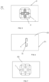
- the integrated radiating element 100 as shown in FIG.
- the integrated radiating element 100 has one-layer PCB 2.
- the balun 3 is coupled to the radiating surface 1.
- a transmission line or feed line is printed or attached to the compact board 2 serving balun 3 for radiating elements.
- the balun 3 can be a single balun for a single polarization or a circular polarization to which a dual-feed balun with one feed having 90 degree offset phase is applied.
- the one-layer compact board 2 is applicable.
- the balun 3 comprise a primary balun 31 and a secondary balun 32 each for one radiating element of dual-polarization as shown in FIGS 4-9 .
- the primary and secondary baluns 31 and 32 each is separately set at one of the two-layer PCB 21, 22 (as shown in FIGS 6 and 8 ) for a good isolation of each port.
- the primary and secondary baluns 31 and 32 can be set on the same plane, such as at the same top surface 23 of the compact board 2 while the radiating surface 1 can be printed on the bottom surface 24 or inner surface 25 of the compact board 2.
- the one-layer compact board 2 can be applicable where the balun 3 and the radiating surface 1 are each attached to the bottom surface 24 and the inner surface 25 of the compact board 2.
- the two-layer compact board 2 composed of PCBs 21 and 22 can also be applicable, where the radiating surface 1 can be attached to the bottom surface 24 or the inner surface 25 while the balun 3 is set on the top surface 23.
- the radiating surface 1 of a radiating element is printed or attached to one surface of the compact board 2, such as the bottom surface 24 or the inner surface 25; where the shape and structure of radiating surface is not limited and can be any type such as circular, square, polygon etched shape.
- the radiating element structure and shape is not limited and half-wave is given as matter of illustration.
- the radiating surface 1 is spaced from the balun 3, and comprises radiating arms (not labeled) adapted for radiating elements of the radiating element.
- the balun 3 is coupled to the radiating surface 1 to form the radiating elements.
- the radiating surface 1 is printed between two PCBs 21 and 22 in a sandwich-like scheme, as shown in FIG. 2 , can be attached such as by printing or etching on any inner surface 25 of the two-layer compact board 2. In other embodiments, the radiating surface 1 is attached such as by printing or etching on the bottom surface 24 of the compact board 2 of one-layer structure (as shown in FIG. 3 ) or two-layer structure.
- Each balun 31, 32 is connected to a transmission line 9 traversing the compact board 2 through hole 23; where the output of the transmission line is connected to RF component device 7 processing signal of interest for a radio unit (not shown).
- the transmission line 9 can be used to support the integrated radiating element 100.
- an integrated antenna unit 200 comprises a dual-polarized radiating element 100 with one radiating element for each polarization.
- Each radiating element is composed of radiating surface 1 and a balun 3.
- the radiating surface 1 of a radiating element is printed between two PCB boards 21 and 22 (sandwich-like scheme); where the shape and structure of radiating surface is not limited and can be any type such as circular, square, polygon etched shape.
- the radiating element structure and shape is not limited and half-wave is given as matter of illustration.
- the balun 3 can be composed of two parts: the first part composed of the compact board 2 where a transmission line or feed line is printed serving the primary balun 31 for one polarization of dual-polarization, and the second part composed of the compact board 2 where a transmission line or feed line is printed serving secondary balun 32 for the other polarization.
- Two baluns 31, 32 are placed on same surface of the board 2. In this case, the two balun (feed lines) 31, 32 are overlapped with a fly-over structure so as to make sure that the two lines are not intersect.
- one of the feed line is broken and re-connected with a 0-Ohm resistor, patch or wire 4; and the compact board 2 can only have one substrate as shown in FIG. 3 , where the baluns 31, 32 are attached on a top surface 23 and the radiating surface 1 is attached on an opposite bottom surface 24 of the compact board 2.
- the balun 3 can be composed of two parts: a first part composed of a primary substrate 21 located on top of the radiating surface 1 where a transmission line is printed serving primary balun 31 for one polarization; a second part composed of a secondary substrate 22 located at bottom of the radiating surface 1 where a transmission line is printed serving secondary balun 32 for the other polarization.
- both the primary substrate 21 and the secondary substrate 22 construct the compact board 2.
- the radiating surface 1 is placed between the primary substrate 21 and the secondary substrate 22.
- the dual-polarized radiating element 100 is connected between two PCBs 21 and 22 serving as balun support of the two polarizations.
- the first polarization has its balun 31 located on top of the upper PCB board 21, denoted as the primary balun 31 while the second one has it at the bottom of the lower board 22, denoted as secondary balun 32.
- the baluns 31, 32 are on same plane as the radiating element.
- the fact of having the primary and secondary baluns 31, 32 printed on a separated board 21, 22 contributes much in terms of inter-port isolation.
- the transmission lines on top of the primary and secondary substrates topology and its length can be tuned to match 50 or 75 Ohm impedance of each radiating element.
- particular rectangular line is used to output bandwidth of more than 44% when a return loss less than -14dB is required covering 1710 ⁇ 2690MHz with good inter-port isolation, stable pattern beamwidth and high-gain for each polarization, as shown in FIG. 12 , which represents S-parameter of compact radiating element (radiating surface with layered-balun).
- Other balun topology can be adopted also with quarter wave transformers to match impedance at desired frequency range.
- the primary and secondary substrates 21, 22 can be manufactured from any type existing PCB materials and its length and thickness can be tuned to match the desired range of interest. Two substrates layers 21, 22 are used to hold the two baluns 31, 32, which leads to a better isolation.
- the two-baluns 31, 32 can be printed on same PCB board acting as substrate.
- the whole integrated radiating element 100 will only need one PCB layer.
- the two baluns (feed lines) 31, 32 are overlapped. And one of the feed line is broken and re-connect the line with a 0-Ohm resistor(low loss line), patch or wire 4.
- the two baluns 31, 32 are placed on the same PCB board. And the whole antenna structure 200 will only need one substrate 2.
- the two balun 31, 32 (feed lines) are overlapped with the feed line being broken and re-connected with a 0-Ohm resistor, patch or wire.
- the integrated radiating element 100 as shown in FIG. 9 is +45° polarization.
- the primary and secondary baluns 31, 32 can be printed on a separated board 21, 22; where similarly, the first polarization has its balun 31 located on top of the upper PCB board 21, while the second one has it at the bottom of the lower board 22. And the baluns 31, 32 are on same plane as the radiating element.
- two baluns 31, 32 can also be placed on the same PCB boardin a fly-over structure, and are overlapped with the feed line being broken and re-connected with a 0-Ohm resistor, patch or wire. The two baluns 31, 32 are spaced from the radiating surface 1.
- the integrated radiating element 100 as shown in FIG. 9 is a single polarization, where the balun 3 is a single balun for a single polarization, and is printed on a top surface of compact board 2 while the radiating surface 1 is printed on the bottom surface of the compact board 2.
- a circular polarization (not shown) to which a dual-feed balun 3 with one feed having 90 degree offset phase is applied.
- the one-layer compact board 2 is applicable.
- the reflecting board 6 is placed below the compact radiating unit 100 with two side walls 61 running parallel enabling to control the 3dB azimuth beam generated by the radiating elements 10.
- the RF component device 7 at least has one input and one output (not labeled) directed connected with the balun 3.
- the RF component device 7 comprises a primary and secondary RF components 71, 72 each has one input and one output connected with each balun 31, 32 for each radiating element.
- the RF component device 7 has one RF component with one input and one output directly connected with the single balun 3.
- the RF component device 7 comprises a primary RF component 71 and secondary RF component 72.
- the primary RF component 71 has one input (not shown) and one output 73 is placed beneath the integrated radiating element 100.
- the primary RF component 71 serves support of the fixture structure of the radiating element 100 to the reflecting board 6. And its output 73 is connected directly to the primary balun 31.
- the connection can be made of cable or any transmission mean 9 traversing the primary and secondary substrates 21 and 22 via hole 23.
- the secondary RF component 72 has one input (not shown) and one output 74 is placed beneath the radiating element 100.
- the secondary RF component 72 also serves support of the fixture structure of the radiating element 100 to the reflecting board 6. And its output 74 is connected directly to the secondary balun 32.
- the connection can be made of cable or any transmission mean 9 traversing the primary and secondary substrates 21 and 22 via hole 23.
- the RF component device 7 is a filtering device which keeps filtered signal of interest which is received from a base station antenna transmitting path or can be forwarded to a base station antenna receiving path.
- the RF component can be band-pass filter in accordance with some embodiments.
- Figure 12 illustrates integrated antenna return loss where a 60MHz band-pass filter with insertion loss less than ldBis used as RF component device.
- the primary and secondary RF components 7 can be housed in same box sharing same cavity or housed in separate boxes with different cavity.
- the parameter adaptation depends on the size and processing performances requested by the base station radio module.
- the integrated antenna unit 200 is proposed in accordance with one embodiment of this invention, where a radiating element 100 is connected between two PCB boards 21, 22 or is attached to a single PCB serving as balun support of the two polarizations. And the baluns 31, 32 are on same plane as the radiating element.
- the space 62 between the radiating element 100 and the reflecting board 6 can be used for RF component device 7 such as phase shifter, filter, amplifier, attenuators.
- RF component device 7 such as phase shifter, filter, amplifier, attenuators.
- Each balun 31, 32 is connected to a transmission line 9 traversing the PCB boards 21, 22 through hole 23; where the output of the transmission line is connected to RF component device 7 processing signal of interest for a radio unit (not shown).
- the RF component device 7 is placed beneath the radiating element 100.
- a reflecting board 6 is placed around 1 ⁇ 4 wavelength of the radiating element 100 where also the RF component device 7 can be fixed.
- FIG. 12 shows an S-parameter of compact radiating element 100 (radiating surface with layered-balun) in accordance with the embodiments of the present invention.
- FIG. 13 shows a return loss of the compact radiating element with filter integrated for one polarization. Both charts show a good radiating performance of the radiating element of the present invention.
- a large-scale array antenna 300 proposed in accordance with an embodiment of the present invention is obtained by collocating several above integrated radiating elements 100, each radiating elements 100 forms a sub-array.
- Multi- array integrated radiating element 100 is supported on the extended reflecting board 6 each by one RF component device 7.
- the extended reflecting board 6 has two parallel side walls 61 running upwards to enclose all the integrated radiating element 100 therebetween.
- the inputs of the multiple band-pass filters 7 can be connected to a radio unit; so that multi-array active antennas can be obtained.
- An antenna-RF component integrated transmission method where a primary RF component 71 proceeds signal of interest from a base station antenna transmitting path.
- the output 73 of the primary RF component 71 is sent to the primary balun 31.
- the primary balun 31 couples its input signal into through the primary substrate 21 and excites the corresponding radiating surface 1 through coupling mechanism.
- a first polarized wave is radiated throughout the space.
- An antenna-RF component integrated transmission method where a secondary RF component 72 proceeds signal of interest from a base station antenna transmitting path.
- the output 74 of the secondary RF component 72 is sent to the secondary balun 32.
- the secondary balun 32 couples its input signal into through the primary substrate 21 and excites the corresponding radiating surface 1 through coupling mechanism.
- a second polarized wave is radiated throughout the space.
- An antenna-RF component integrated receiving method where a radiating element 100 sends its received polarized wave to the primary balun 31.
- the output of the primary balun 31 is forwarded to the primary RF component 71 which proceeds signal of interest that can be sent to a base station antenna receiving path.
- An antenna-RF component integrated receiving method where a radiating element sends its received polarized wave to the secondary balun 32.
- the output of the secondary balun 32 is forwarded to the secondary RF component 72 which proceeds signal of interest that can be sent to a base station antenna receiving path.
- the term “comprising”, “comprises” or “composed of” is intended to mean that the devices, systems, and methods include the recited elements, and may additionally include any other elements.
- Consisting essentially of shall mean that the devices, systems, and methods include the recited elements and exclude other elements of essential significance to the combination for the stated purpose. Thus, a system or method consisting essentially of the elements as defined herein would not exclude other materials, features, or steps that do not materially affect the basic and novel characteristic(s) of the claimed invention.
- Consisting of shall mean that the devices, systems, and methods include the recited elements and exclude anything more than a trivial or inconsequential element or step. Embodiments defined by each of these transitional terms are within the scope of this disclosure.
Landscapes
- Engineering & Computer Science (AREA)
- Computer Networks & Wireless Communication (AREA)
- Signal Processing (AREA)
- Physics & Mathematics (AREA)
- Electromagnetism (AREA)
- Variable-Direction Aerials And Aerial Arrays (AREA)
- Aerials With Secondary Devices (AREA)
Description
- This application generally relates to the field of communication system, and particularly, to an integrated antenna unit and a multi-array antenna of the same.
- In traditional phased-array antennas, a set of radiating elements (known as sub- arrays) are combined in the vertical plane to boost more gain. Also, a cavity backed component such as filter, phase shifter, amplifier or attenuator is generally used at the back of the whole antenna with number of outputs same as the number of sub-array ports with additional connectors. And the inputs of the cavity -backed component are connected to a number of Transmitting/Receiving circuits (from RRU); which heavily increase antenna dimension and complexity of feed line since the multiple sub-arrays impose to have additional power splitters to be with feed lines. Also, it can be noted extra weight and cost with multiple cavities and additional connectors and wasted space between radiating surface and antenna reflector due to the fact that existing design is having balun being supported by a fixture structure. In addition, this imposes costly development and implementation resources as multiple soldering points between radiating elements, power splitters and feeding network.
-
CN 105 960 737 A describes a multi-frequency communications antenna and a base station. -
US 2013/214982 A1 discloses an antenna unit with a radiating element above an electrically conductive ground plane, the radiating element comprising a board with a dipole on its top or bottom layer and a grounded conductive area on its bottom or top layer, the radiating element supported by a dielectric filling or coaxial cable. - A main object of the present invention is to provide an antenna unit, which can simplify the antenna-array structure, improve the antenna capacity and exploitation with good radiating performance.
- A secondary object of the present invention is to provide a multi-array antenna, which can obtain a Massive MIMO antenna.
- A further object of the present invention is to provide an antenna-RF component integrated transmission method.
- A final object of the present invention is to provide an antenna-RF component integrated receiving method.
- To obtain the above object, an integrated antenna unit provided in the present invention comprising: an integrated radiating element; a reflect board beneath the integrated radiating element without a direct contact therebetween; and an RF component device for processing signal of interest for a radio unit. The RF component device is placed beneath the integrated radiating element and on the reflecting board, and serves a support of a fixture structure of the radiating element to the reflecting board; whereby a space between the radiating element and the reflecting board can be efficiently used for the RF component device.
- In some embodiments, the RF component device can be one of a phase shifter, a filter, an amplifier, and an attenuator; the radiating element is dual-polarization, single- polarization, or circular polarization.
- In some embodiments, the integrated radiating element comprises a balun and a radiating surface separately coupled to each other; the integrated antenna unit further comprises a compact board to hold the balun.
- In some embodiments, the same baluns are set in the same plane; the radiating surface is integrated with the compact board.
- In some embodiments, a transmission line is attached on the compact board serving the balun.
- In some embodiments, the transmission lines on the compact board topology and its length are tuned to match 50 or 75 Ohm impedance of each radiating element.
- In some embodiments, the compact board is made from any type PCB materials, and its length and thickness are tuned to match a desired band range of interest signal.
- In some embodiments, the compact board has one or two substrates.
- In some embodiments, the balun comprises two parts: a first part where the transmission line attached on the compact board serves a primary balun for one polarization; a second part where the transmission line is attached on the compact board serving a secondary balun for the other polarization.
- In some embodiments, the primary balun is printed on a primary substrate located on top of the radiating surface; the secondary balun is printed on a secondary substrate located at a bottom of the radiating surface; the primary substrate and the secondary substrate construct the compact board; and the radiating surface is placed between the primary substrate and the secondary substrate.
- In some embodiments, the primary balun and the secondary baluns are overlapped with a fly-over structure and attached on the same plane of the compact board; two baluns are not intersect with each other; and one of the baluns is broken, and reconnect with a 0-Ohm resistor, patch or wire..
- In some embodiments, the overlapped baluns and the radiating surface are located at opposite surface of the compact board.
- In some embodiments, the transmission line is attached on a top surface of the compact board serves the balun for a single polarization; the radiating surface is attached on a bottom surface of the compact board.
- In some embodiments, the RF component device at least has one input and one output; the output of the RF component device directly connected with the balun.
- In some embodiments, the RF component device comprise a primary RF component and a secondary RF component each with one output directly connected with the primary balun and the secondary balun; the connection can be made of any transmission mean traversing the primary and secondary substrates via hole.
- In some embodiments, the primary and secondary RF components can be housed in same box sharing same cavity or housed in separate boxes with different cavity; the parameter adaptation is adapted for a size and processing performances requested by the base station radio module.
- In some embodiments, the reflecting board is placed below the integrated radiating element with two side walls running parallel; a height of the side walls can be tuned to control desired 3dB azimuth beam of the radiating elements.
- To obtain the above object, a multi-array antenna provided in the present invention comprising: multiple antenna units, the multiple antenna units are supported on the reflecting board, and two running side wall enclose the antenna units therebetween.
- In some embodiments, the multi-array antenna has multiple band-pass filters as the RF component, the multiple band-pass filters are connected to a radio unit thus to form a multi- array active antenna.
- To obtain the above object, an antenna-RF component integrated transmission method comprises: proceeding signal of interest from a base station antenna transmitting path by a primary RF component; sending an output of the primary RF component to a primary balun; coupling an input signal by the primary balun into through a primary substrate and exciting a corresponding radiating surface through coupling mechanism; and radiating a first polarized wave throughout the space.
- To obtain the above object, an antenna-RF component integrated transmission method comprises: proceeding signal of interest from a base station antenna transmitting path by a secondary RF component; sending an output of the secondary RF component to a secondary balun; coupling an input signal of the secondary balun into through the primary substrate and exciting a corresponding radiating surface through coupling mechanism; and radiating a second polarized wave throughout the space.
- To obtain the above object, an antenna-RF component integrated receiving method provided in the present invention comprising: sending received polarized wave to a primary balun by an integrated radiating element; forwarding output of the primary balun to a primary RF component which proceeds signal of interest; and sending signal of interest to a base station antenna receiving path.
- To obtain the above object, an antenna-RF component integrated receiving method,
provided in the present invention comprising: sending received polarized wave to a secondary balun by a radiating element; forwarding the output of the secondary balun to a secondary RF component which proceeds signal of interest; and sending signal of interest to a base station antenna receiving path. - In accordance with the embodiments, the present invention has advantages that: a compact antenna element unit can be obtained since the radiating elements are integrated with a compact printed board; further, the baluns of two polarizations respectively set on a separated board contributes much in terms of inter-port isolation, ease of antenna feeding drawing, a stable pattern beam width and high-gain. And a compact sized of the antenna can be obtained.
- Further, the antenna unit has a simple structure and high capacity because of the compact antenna element, and the space between the radiating elements and the reflecting board can be used efficiently by adding a compact band-pass filter therebetween, and cost effective compact integrated antenna unit can be obtained which is also easy to manufacture especially.
- A large scale MIMO antenna is to be produced as there are less soldering parts and reduced connectors.
- The above-mentioned features, as well as other features, aspects, and advantages of the present technology will now be described in connection with various embodiments of the invention, in reference to the accompanying drawings. The illustrated embodiments, however, are merely examples and are not intended to limit the invention.
-
-
FIG. 1 illustrates a cross-sectional view of an integrated antenna unit in accordance with an embodiment of the present invention; -
FIG. 2 illustrates a cross-sectional view of an integrated radiating element in accordance with one embodiment of the present invention; -
FIG. 3 illustrates a cross-sectional view of an integrated radiating element in accordance with another embodiment of the present invention; -
FIG. 4 illustrates an integrated radiating element in accordance with one embodiment of the present invention, where (a) represents a perspective view thereof, (b) a top plane view thereof, and (c) represents a bottom view thereof; -
FIG. 5 illustrates a schematic diagram of the integrated radiating element of dual polarization in accordance with one embodiment of the present invention; -
FIG. 6 illustrates a plane view of the radiating element in accordance with one embodiment of the present invention; -
FIG. 7 illustrates a plane view of an inner surface of the radiating element in accordance with one embodiment of the present invention; -
FIG. 8 illustrates a rear view of the radiating element in accordance with one embodiment of the present invention; -
FIG. 9 illustrates a perspective view of the integrated radiating element in accordance with one embodiment of the present invention; -
FIG. 10 illustrates a perspective view of the integrated radiating element in accordance with one embodiment of the present invention; -
FIG. 11 illustrate a perspective view of a large-scale array in accordance with one embodiment of the present invention; -
FIG. 12 represents the S-parameters of one radiating element (radiating surface with layered-balun) in accordance with an embodiment of the present invention; and -
FIG. 13 represents a return loss of a compact radiating element with filter integrated for one polarization in accordance with an embodiment of the present invention. - The provided figures and the following description of certain embodiments of the invention are not intended to limit the invention to these embodiments, but rather, are provided to enable any person skilled in the art to make and use this invention.
- Referring to
FIGS 1-3 , an integratedantenna unit 200 is proposed in accordance with one embodiment of this invention, comprise an integratedradiating element 100 integrated with acompact board 2, areflect board 6 beneath the integratedradiating element 100, and anRF component device 7 fixed on the reflectingboard 6 and beneath theradiating element 100. TheRF component device 7 is accommodated in aspace 62 between the radiatingelement 100 and the reflectingboard 6, and supports the radiatingelement 100 without extra fixture structure. TheRF component device 7 can be phase shifter, filter, amplifier, attenuators, or others. TheRF component device 7 is used to process signals from a base station antenna transmitting path or from the radiatingelement 100. - The
integrated radiating element 100 comprises abalun 3 and a radiatingsurface 1 integrated on thecompact board 2. Thecompact board 2 can be manufactured from any type existing PCB materials and its length and thickness can be tuned to match the desired range of interest, and at least has one substrate. Other substrate materials adapted for the radiating element can also be used. Thecompact board 2 has atop surface 23 and anopposite bottom surface 24, and can be one-layer structure (as shown inFIG. 3 ); or can be two-layer structure(as shown inFIG. 2 ), denoted as aprimary substrate 21 and asecondary substrate 22 each with aninner surface 25 opposite. Theintegrated radiating element 100 as shown inFIG. 2 has thecompact board 2 composed of two layers ofPCB top PCB 21 and abottom PCB 22 using the same reference number of the substrate, each with theinner surface 25 overlapped. While inFIG. 3 , theintegrated radiating element 100 has one-layer PCB 2. - The
balun 3 is coupled to the radiatingsurface 1. In this invention, a transmission line or feed line is printed or attached to thecompact board 2 servingbalun 3 for radiating elements. - In some embodiments, referring to
FIGS 3 and10 , thebalun 3 can be a single balun for a single polarization or a circular polarization to which a dual-feed balun with one feed having 90 degree offset phase is applied. In this case, the one-layercompact board 2 is applicable. - In other embodiments, the
balun 3 comprise aprimary balun 31 and asecondary balun 32 each for one radiating element of dual-polarization as shown inFIGS 4-9 . In some embodiments, the primary andsecondary baluns layer PCB 21, 22 (as shown inFIGS 6 and8 ) for a good isolation of each port. - In other embodiments, the primary and
secondary baluns top surface 23 of thecompact board 2 while the radiatingsurface 1 can be printed on thebottom surface 24 orinner surface 25 of thecompact board 2. Referring toFIGS 4(a) ,5 and9 . In this case, the one-layercompact board 2 can be applicable where thebalun 3 and the radiatingsurface 1 are each attached to thebottom surface 24 and theinner surface 25 of thecompact board 2. And further in other embodiments, the two-layercompact board 2 composed ofPCBs surface 1 can be attached to thebottom surface 24 or theinner surface 25 while thebalun 3 is set on thetop surface 23. - The radiating
surface 1 of a radiating element is printed or attached to one surface of thecompact board 2, such as thebottom surface 24 or theinner surface 25; where the shape and structure of radiating surface is not limited and can be any type such as circular, square, polygon etched shape. The radiating element structure and shape is not limited and half-wave is given as matter of illustration. The radiatingsurface 1 is spaced from thebalun 3, and comprises radiating arms (not labeled) adapted for radiating elements of the radiating element. Thebalun 3 is coupled to the radiatingsurface 1 to form the radiating elements. - In some embodiments, the radiating
surface 1 is printed between twoPCBs FIG. 2 , can be attached such as by printing or etching on anyinner surface 25 of the two-layercompact board 2. In other embodiments, the radiatingsurface 1 is attached such as by printing or etching on thebottom surface 24 of thecompact board 2 of one-layer structure (as shown inFIG. 3 ) or two-layer structure. - Each
balun transmission line 9 traversing thecompact board 2 throughhole 23; where the output of the transmission line is connected toRF component device 7 processing signal of interest for a radio unit (not shown). Thetransmission line 9 can be used to support theintegrated radiating element 100. - The following illustrates more detail of various embodiments of the
integrated radiating element 100 of the present invention. - In a first embodiment, an
integrated antenna unit 200 comprises a dual-polarized radiating element 100 with one radiating element for each polarization. Each radiating element is composed of radiatingsurface 1 and abalun 3. - The radiating
surface 1 of a radiating element is printed between twoPCB boards 21 and 22 (sandwich-like scheme); where the shape and structure of radiating surface is not limited and can be any type such as circular, square, polygon etched shape. The radiating element structure and shape is not limited and half-wave is given as matter of illustration. - In some embodiments, referring to
FIGS 4(a)-(c) which illustrates aradiating element 100 of dual polarization, thebalun 3 can be composed of two parts: the first part composed of thecompact board 2 where a transmission line or feed line is printed serving theprimary balun 31 for one polarization of dual-polarization, and the second part composed of thecompact board 2 where a transmission line or feed line is printed servingsecondary balun 32 for the other polarization. Twobaluns board 2. In this case, the two balun (feed lines) 31, 32 are overlapped with a fly-over structure so as to make sure that the two lines are not intersect. In an embodiment, one of the feed line is broken and re-connected with a 0-Ohm resistor, patch orwire 4; and thecompact board 2 can only have one substrate as shown inFIG. 3 , where thebaluns top surface 23 and the radiatingsurface 1 is attached on anopposite bottom surface 24 of thecompact board 2. - In other embodiments, referring to
FIGS 5-8 together, thebalun 3 can be composed of two parts: a first part composed of aprimary substrate 21 located on top of the radiatingsurface 1 where a transmission line is printed servingprimary balun 31 for one polarization; a second part composed of asecondary substrate 22 located at bottom of the radiatingsurface 1 where a transmission line is printed servingsecondary balun 32 for the other polarization. In this case, both theprimary substrate 21 and thesecondary substrate 22 construct thecompact board 2. The radiatingsurface 1 is placed between theprimary substrate 21 and thesecondary substrate 22. - The dual-
polarized radiating element 100 is connected between twoPCBs balun 31 located on top of theupper PCB board 21, denoted as theprimary balun 31 while the second one has it at the bottom of thelower board 22, denoted assecondary balun 32. And thebaluns secondary baluns board - The transmission lines on top of the primary and secondary substrates topology and its length can be tuned to match 50 or 75 Ohm impedance of each radiating element. As matter of illustration, particular rectangular line is used to output bandwidth of more than 44% when a return loss less than -14dB is required covering 1710~2690MHz with good inter-port isolation, stable pattern beamwidth and high-gain for each polarization, as shown in
FIG. 12 , which represents S-parameter of compact radiating element (radiating surface with layered-balun). Other balun topology can be adopted also with quarter wave transformers to match impedance at desired frequency range. - The primary and
secondary substrates baluns - In other embodiments as shown in
FIG. 4 , the two-baluns element 100 will only need one PCB layer. In this case, the two baluns (feed lines) 31, 32 are overlapped. And one of the feed line is broken and re-connect the line with a 0-Ohm resistor(low loss line), patch orwire 4. In this embodiment, the twobaluns whole antenna structure 200 will only need onesubstrate 2. In this case, the twobalun 31, 32 (feed lines) are overlapped with the feed line being broken and re-connected with a 0-Ohm resistor, patch or wire. - The
integrated radiating element 100 as shown inFIG. 9 is +45° polarization. The primary andsecondary baluns board balun 31 located on top of theupper PCB board 21, while the second one has it at the bottom of thelower board 22. And thebaluns baluns baluns surface 1. - The
integrated radiating element 100 as shown inFIG. 9 is a single polarization, where thebalun 3 is a single balun for a single polarization, and is printed on a top surface ofcompact board 2 while the radiatingsurface 1 is printed on the bottom surface of thecompact board 2. - In other embodiment, a circular polarization (not shown) to which a dual-
feed balun 3 with one feed having 90 degree offset phase is applied. In this case, the one-layercompact board 2 is applicable. - Referring
FIG. 1 again, in theantenna unit 200 of the present invention, the reflectingboard 6 is placed below thecompact radiating unit 100 with twoside walls 61 running parallel enabling to control the 3dB azimuth beam generated by the radiatingelements 10. - The
RF component device 7 at least has one input and one output (not labeled) directed connected with thebalun 3. As for a dual-polarized orcircular radiating element 100, theRF component device 7 comprises a primary andsecondary RF components balun - It is understood, as for a single polarization, the
RF component device 7 has one RF component with one input and one output directly connected with thesingle balun 3. - In one embodiment as shown in
FIG. 1 , theRF component device 7 comprises aprimary RF component 71 andsecondary RF component 72. Theprimary RF component 71 has one input (not shown) and oneoutput 73 is placed beneath theintegrated radiating element 100. Theprimary RF component 71 serves support of the fixture structure of the radiatingelement 100 to the reflectingboard 6. And itsoutput 73 is connected directly to theprimary balun 31. The connection can be made of cable or any transmission mean 9 traversing the primary andsecondary substrates hole 23. - The
secondary RF component 72 has one input (not shown) and oneoutput 74 is placed beneath the radiatingelement 100. Thesecondary RF component 72 also serves support of the fixture structure of the radiatingelement 100 to the reflectingboard 6. And itsoutput 74 is connected directly to thesecondary balun 32. The connection can be made of cable or any transmission mean 9 traversing the primary andsecondary substrates hole 23. - In some embodiments, the
RF component device 7 is a filtering device which keeps filtered signal of interest which is received from a base station antenna transmitting path or can be forwarded to a base station antenna receiving path. The RF component can be band-pass filter in accordance with some embodiments.Figure 12 illustrates integrated antenna return loss where a 60MHz band-pass filter with insertion loss less than ldBis used as RF component device. - The primary and
secondary RF components 7 can be housed in same box sharing same cavity or housed in separate boxes with different cavity. The parameter adaptation depends on the size and processing performances requested by the base station radio module. - The
integrated antenna unit 200 is proposed in accordance with one embodiment of this invention, where aradiating element 100 is connected between twoPCB boards baluns - There is no direct contact between the radiating
element 100 and its grounding plane (reflecting board) 6. So, thespace 62 between the radiatingelement 100 and the reflectingboard 6 can be used forRF component device 7 such as phase shifter, filter, amplifier, attenuators. Eachbalun transmission line 9 traversing thePCB boards hole 23; where the output of the transmission line is connected toRF component device 7 processing signal of interest for a radio unit (not shown). TheRF component device 7 is placed beneath the radiatingelement 100. A reflectingboard 6 is placed around ¼ wavelength of the radiatingelement 100 where also theRF component device 7 can be fixed. Interestingly, thespace 62 between the radiatingelements 10 and the reflectingboard 6 can be used efficiently and theback 60 of the reflecting board can be used as support of other components for an active antenna array. So cost effectiveintegrated unit 200 is obtained which is also easy to manufacture especially when large scale active antenna array is to be produced as there are less soldering parts and reduced number of connectors.FIG. 12 shows an S-parameter of compact radiating element 100 (radiating surface with layered-balun) in accordance with the embodiments of the present invention.FIG. 13 shows a return loss of the compact radiating element with filter integrated for one polarization. Both charts show a good radiating performance of the radiating element of the present invention. - Referring to
FIG.11 , a large-scale array antenna 300 proposed in accordance with an embodiment of the present invention is obtained by collocating several above integrated radiatingelements 100, each radiatingelements 100 forms a sub-array. Multi- array integrated radiatingelement 100 is supported on the extended reflectingboard 6 each by oneRF component device 7. Thus theMIMO antenna 300 has multipleRF component device 7 each processing signal of interest for a radio unit. The extended reflectingboard 6 has twoparallel side walls 61 running upwards to enclose all theintegrated radiating element 100 therebetween. - Further, the inputs of the multiple band-
pass filters 7 can be connected to a radio unit; so that multi-array active antennas can be obtained. - An antenna-RF component integrated transmission method, where a
primary RF component 71 proceeds signal of interest from a base station antenna transmitting path. Theoutput 73 of theprimary RF component 71 is sent to theprimary balun 31. And theprimary balun 31 couples its input signal into through theprimary substrate 21 and excites the corresponding radiatingsurface 1 through coupling mechanism. A first polarized wave is radiated throughout the space. - An antenna-RF component integrated transmission method, where a
secondary RF component 72 proceeds signal of interest from a base station antenna transmitting path. Theoutput 74 of thesecondary RF component 72 is sent to thesecondary balun 32. And thesecondary balun 32 couples its input signal into through theprimary substrate 21 and excites the corresponding radiatingsurface 1 through coupling mechanism. A second polarized wave is radiated throughout the space. - An antenna-RF component integrated receiving method, where a
radiating element 100 sends its received polarized wave to theprimary balun 31. The output of theprimary balun 31 is forwarded to theprimary RF component 71 which proceeds signal of interest that can be sent to a base station antenna receiving path. - An antenna-RF component integrated receiving method, where a radiating element sends its received polarized wave to the
secondary balun 32. The output of thesecondary balun 32 is forwarded to thesecondary RF component 72 which proceeds signal of interest that can be sent to a base station antenna receiving path. - As used in the description and claims, the singular form "a", "an" and "the" include both singular and plural references unless the context clearly dictates otherwise. At times, the claims and disclosure may include terms such as "a plurality," "one or more," or "at least one;" however, the absence of such terms is not intended to mean, and should not be interpreted to mean, that a plurality is not conceived.
- As used herein, the term "comprising", "comprises" or "composed of" is intended to mean that the devices, systems, and methods include the recited elements, and may additionally include any other elements. "Consisting essentially of" shall mean that the devices, systems, and methods include the recited elements and exclude other elements of essential significance to the combination for the stated purpose. Thus, a system or method consisting essentially of the elements as defined herein would not exclude other materials, features, or steps that do not materially affect the basic and novel characteristic(s) of the claimed invention. "Consisting of" shall mean that the devices, systems, and methods include the recited elements and exclude anything more than a trivial or inconsequential element or step. Embodiments defined by each of these transitional terms are within the scope of this disclosure.
- The examples and illustrations included herein show, by way of illustration and not of limitation, specific embodiments in which the subject matter may be practiced. Other embodiments may be utilized and derived therefrom, such that structural and logical substitutions and changes may be made without departing from the scope of the appended claims defining the invention.
Claims (9)
- An antenna unit (200) comprising:a radiating element (100) comprising a board (2) defining a first radiating surface (1) and an opposing second surface;a reflect board (6) having a first support surface and an opposing second surface, the radiating element and the reflect board are arranged such that the first support surface of the reflect board faces the first radiating surface of the radiating element (100) forming a space therebetween; andan RF device (7) for processing signal of interest for a radio unit;wherein the RF device (7) is placed on the first support surface of the reflect board (6) and is arranged in the space between the radiating element (100) and the reflect board (6), such that the RF device (7) serves as a support structure for the radiating element (100) to the reflect board (6);wherein the radiating element (100) further comprises a balun (3) coupled to the first radiating surface (1); wherein a transmission line or feed line of the antenna unit (200) is connected to the balun (3), the balun (3) being on the opposing second surface of the board (2);wherein the transmission line is attached to the opposing second surface of the board (2) and serves the balun for a single polarization.
- The antenna unit (200) according to claim 1, wherein the balun (3) comprises two parts: a first part where the transmission line attached on the board (2) serves a primary balun for one polarization; a second part where the transmission line is attached on the board (2) serving a secondary balun for the other polarization.
- The antenna unit (200) according to claim 2, characterized in that the primary balun is printed on a primary substrate located on top of the radiating surface (1); the secondary balun is printed on a secondary substrate located at a bottom of the radiating surface (1); the primary substrate and the secondary substrate construct the board (2); and the radiating surface (1) is placed between the primary substrate and the secondary substrate; or
characterized in that the primary balun and the secondary baluns are overlapped with a fly-over structure, two baluns are not intersect with each other; and baluns are attached on the same plane of the board (2); one of the baluns is broken, and re-connect with a 0-Ohm resistor, patch or wire. - The antenna unit (200) according to any one of claims 1 to 3, wherein the RF device (7) at least has one input and one output; the output of the RF device (7) being directly connected with the balun.
- The antenna unit (200) according to claim 4, wherein the RF device (7) comprises a primary RF component and a secondary RF component each with one output directly connected with the primary balun and the secondary balun; the connection can be made of any transmission means traversing the primary and secondary substrates via a hole (23); or
characterized in that the primary and secondary RF components can be housed in same box sharing same cavity or housed in separate boxes with different cavity; a parameter adaptation of the RF component device (7) is adapted for a size and processing performances requested by the base station radio module. - The antenna unit (200) according to claim 1, wherein the reflect board is placed below the radiating element (100) with two side walls running parallel; a height of the side walls is configured to be tunable to control desired 3dB azimuth beam of the radiating elements (100).
- A multi-array antenna comprising multiple antenna units according to claims 1 to 6, wherein the multiple antenna units are supported on the reflect board and located between two running side walls thereof.
- The multi-array antenna according to claim 7, wherein the multi-array antenna has multiple band-pass filters as the RF component, the multiple band-pass filters each are connected to a radio unit of the multi-array antenna thus to form a multi-array active antenna.
- An antenna unit (200) comprising:a radiating element (100) comprising a board (2) having a top surface (23) and an opposite bottom surface (24) and comprising at least two substrates (21, 22) with an inner surface (25) between the two substrates,the inner surface being a first radiating surface;a reflect board (6) having a first support surface and an opposing second surface,the radiating element and the reflect board are arranged such that the first support surface of the reflect board faces the bottom surface (24) of the radiating element (100) forming a space therebetween;and an RF device (7) for processing signal of interest for a radio unit;wherein the RF device (7) is placed on the first support surface of the reflect board (6) and is arranged in the space between the radiating element (100) and the reflect board (6),such that the RF device (7) serves as a support structure for the radiating element (100) to the reflect board (6);wherein the radiating element (100) further comprises a balun (3) coupled to the first radiating surface (1);the balun (3) being on at least one of the top surface (23) or the bottom surface (24) of the board;wherein a transmission line or of the antenna unit (200) feed line is connected to the balun (3);wherein the transmission line is attached to the top surface (23) or the bottom surface (24) of the board (2) and serves the balun for a single polarization.
Applications Claiming Priority (1)
| Application Number | Priority Date | Filing Date | Title |
|---|---|---|---|
| PCT/CN2017/084200 WO2018205277A1 (en) | 2017-05-12 | 2017-05-12 | Integrated antenna unit, multi-array antenna, transmission method and receiving method of same |
Publications (4)
| Publication Number | Publication Date |
|---|---|
| EP3622578A1 EP3622578A1 (en) | 2020-03-18 |
| EP3622578A4 EP3622578A4 (en) | 2020-11-25 |
| EP3622578C0 EP3622578C0 (en) | 2025-01-29 |
| EP3622578B1 true EP3622578B1 (en) | 2025-01-29 |
Family
ID=62135214
Family Applications (1)
| Application Number | Title | Priority Date | Filing Date |
|---|---|---|---|
| EP17909600.3A Active EP3622578B1 (en) | 2017-05-12 | 2017-05-12 | Integrated antenna unit, multi-array antenna, transmission method and receiving method of same |
Country Status (4)
| Country | Link |
|---|---|
| US (1) | US11128036B2 (en) |
| EP (1) | EP3622578B1 (en) |
| CN (1) | CN108063318B (en) |
| WO (1) | WO2018205277A1 (en) |
Families Citing this family (18)
| Publication number | Priority date | Publication date | Assignee | Title |
|---|---|---|---|---|
| US20190044258A1 (en) * | 2017-08-07 | 2019-02-07 | Commscope Technologies Llc | Cable connector block assemblies for base station antennas |
| EP3599664B1 (en) * | 2018-07-27 | 2022-08-31 | Xilinx, Inc. | Antenna module and massive mimo antenna |
| US10938121B2 (en) * | 2018-09-04 | 2021-03-02 | Mediatek Inc. | Antenna module of improved performances |
| CN109326891B (en) * | 2018-10-16 | 2024-01-05 | 广东通宇通讯股份有限公司 | An AAU front-end structure for 5G wireless communication equipment |
| CN110137665A (en) * | 2019-04-30 | 2019-08-16 | 东莞弗兰德通信科技有限公司 | Integrated antenna array and base station |
| CN112186330A (en) * | 2019-07-03 | 2021-01-05 | 康普技术有限责任公司 | Base station antenna |
| CN113140893B (en) | 2020-01-20 | 2026-01-30 | 户外无线网络有限公司 | Compact broadband dual-polarized radiating element for base station antenna applications |
| EP3852193A1 (en) * | 2020-01-20 | 2021-07-21 | CommScope Technologies LLC | Compact wideband dual-polarized radiating elements for base station antenna applications |
| EP3934023A1 (en) * | 2020-06-29 | 2022-01-05 | Kaelus Antennas AB | Antenna element and antenna comprising antenna elements |
| KR102928268B1 (en) * | 2020-09-21 | 2026-02-19 | 삼성전자주식회사 | Antenna structure and electronic device including the same |
| WO2022067486A1 (en) * | 2020-09-29 | 2022-04-07 | Telefonaktiebolaget Lm Ericsson (Publ) | Base station |
| CN116420283B (en) * | 2020-12-11 | 2025-02-11 | 华为技术有限公司 | Base station antenna and base station equipment |
| CN112713396B (en) * | 2020-12-21 | 2022-10-18 | 北京机电工程研究所 | A dual-frequency miniaturized dipole antenna with a rectangular cavity |
| CN113241519B (en) * | 2021-03-22 | 2023-01-31 | 广东通宇通讯股份有限公司 | Integrated antenna system |
| CN113437488B (en) * | 2021-06-07 | 2023-04-28 | 京信通信技术(广州)有限公司 | Multi-frequency array antenna, radiation structure and assembly method of radiation structure |
| CN115911820A (en) * | 2021-09-22 | 2023-04-04 | 安弗施无线射频系统(上海)有限公司 | Antennas and base stations |
| WO2023206005A1 (en) * | 2022-04-25 | 2023-11-02 | 京东方科技集团股份有限公司 | Dual-polarized antenna and electronic device |
| CN119994426B (en) * | 2025-04-11 | 2025-06-06 | 佛山市波谱达通信科技有限公司 | A multi-cavity coaxial transmission line structure for antenna feeding network |
Citations (3)
| Publication number | Priority date | Publication date | Assignee | Title |
|---|---|---|---|---|
| KR101107295B1 (en) * | 2011-03-31 | 2012-01-20 | 주식회사 선우커뮤니케이션 | Dual polarized dipole antenna |
| KR20130060981A (en) * | 2011-11-30 | 2013-06-10 | 박진영 | The structure of dual polarization dipole antenna |
| US20160372839A1 (en) * | 2015-06-20 | 2016-12-22 | Huawei Technologies Co., Ltd. | Antenna Element for Signals with Three Polarizations |
Family Cites Families (14)
| Publication number | Priority date | Publication date | Assignee | Title |
|---|---|---|---|---|
| US7692601B2 (en) * | 2002-12-13 | 2010-04-06 | Andrew Llc | Dipole antennas and coaxial to microstrip transitions |
| US20110260941A1 (en) * | 2008-10-15 | 2011-10-27 | Argus Technologies (Australia) Pty Ltd. | Wideband radiating elements |
| KR101304929B1 (en) * | 2011-11-30 | 2013-09-11 | 박진영 | Triple band dual Polarization Dipole Antenna including balun based on Printed Circuit Board |
| US8830135B2 (en) * | 2012-02-16 | 2014-09-09 | Ultra Electronics Tcs Inc. | Dipole antenna element with independently tunable sleeve |
| CN106104914B (en) * | 2014-04-11 | 2019-02-22 | 康普技术有限责任公司 | Method for cancelling resonance in a multiband radiating array |
| CN204118242U (en) | 2014-07-14 | 2015-01-21 | 广州杰赛科技股份有限公司 | Wideband dual-polarization radiating unit and array antenna |
| US9577318B2 (en) * | 2014-08-19 | 2017-02-21 | Apple Inc. | Electronic device with fingerprint sensor and tunable hybrid antenna |
| CN204011714U (en) | 2014-08-25 | 2014-12-10 | 罗森伯格技术(昆山)有限公司 | Dual polarization vibrator |
| US9905938B2 (en) | 2015-01-29 | 2018-02-27 | City University Of Hong Kong | Dual polarized high gain and wideband complementary antenna |
| US20170062940A1 (en) * | 2015-08-28 | 2017-03-02 | Amphenol Corporation | Compact wideband dual polarized dipole |
| CN106797075B (en) * | 2015-08-31 | 2020-08-07 | 华为技术有限公司 | An antenna element for dual polarization of multi-frequency antenna |
| CN105960737B (en) * | 2015-12-03 | 2019-08-20 | 华为技术有限公司 | A kind of multi-band communication antenna and base station |
| CN105896071B (en) * | 2016-04-27 | 2019-07-12 | 上海安费诺永亿通讯电子有限公司 | Dual polarization vibrator unit, antenna and multifrequency antenna array |
| CN206076502U (en) | 2016-08-17 | 2017-04-05 | 深圳市普方众智精工科技有限公司 | Vertical polarization ceiling mount antenna and bipolar omni-directional ceiling antenna |
-
2017
- 2017-05-12 EP EP17909600.3A patent/EP3622578B1/en active Active
- 2017-05-12 US US16/478,950 patent/US11128036B2/en active Active
- 2017-05-12 WO PCT/CN2017/084200 patent/WO2018205277A1/en not_active Ceased
- 2017-11-30 CN CN201711236842.7A patent/CN108063318B/en active Active
Patent Citations (3)
| Publication number | Priority date | Publication date | Assignee | Title |
|---|---|---|---|---|
| KR101107295B1 (en) * | 2011-03-31 | 2012-01-20 | 주식회사 선우커뮤니케이션 | Dual polarized dipole antenna |
| KR20130060981A (en) * | 2011-11-30 | 2013-06-10 | 박진영 | The structure of dual polarization dipole antenna |
| US20160372839A1 (en) * | 2015-06-20 | 2016-12-22 | Huawei Technologies Co., Ltd. | Antenna Element for Signals with Three Polarizations |
Also Published As
| Publication number | Publication date |
|---|---|
| EP3622578A1 (en) | 2020-03-18 |
| WO2018205277A1 (en) | 2018-11-15 |
| EP3622578C0 (en) | 2025-01-29 |
| CN108063318B (en) | 2021-01-26 |
| CN108063318A (en) | 2018-05-22 |
| EP3622578A4 (en) | 2020-11-25 |
| US20200044327A1 (en) | 2020-02-06 |
| US11128036B2 (en) | 2021-09-21 |
Similar Documents
| Publication | Publication Date | Title |
|---|---|---|
| US11128036B2 (en) | Integrated antenna unit, multi-array antenna, transmission method and receiving method of same | |
| EP3622583B1 (en) | Integrated antenna element, antenna unit, multi-array antenna, transmission method and receiving method of same | |
| CN112117533B (en) | Dual Frequency Dual Linear Polarization Phased Array Antenna and Antenna Unit | |
| CN111786133B (en) | A Transceiver Common Aperture Phased Array Antenna | |
| US5892482A (en) | Antenna mutual coupling neutralizer | |
| EP3408891B1 (en) | Radiating integrated antenna unit and multi-array antenna of same | |
| EP3526855B1 (en) | Single layer shared aperture dual band antenna | |
| CN111052504A (en) | Millimeter wave antenna array element, array antenna and communication product | |
| WO2011094121A1 (en) | Method and apparatus for tri-band feed with pseudo-monopulse tracking | |
| US9728855B2 (en) | Broadband GNSS reference antenna | |
| CN112242612B (en) | Patch Antenna | |
| CN114122698A (en) | An integrated three-frequency Beidou navigation antenna | |
| CN110676568B (en) | A dual circular polarization microstrip antenna unit | |
| WO2007060782A1 (en) | Multifrequency microstrip antenna | |
| CN206076497U (en) | Same polarization micro-strip duplexed antenna array | |
| CN119054153A (en) | Matching network decoupled between polarizations of antenna array and electronic device comprising same | |
| CN113036401A (en) | Half-wave oscillator, half-wave oscillator component and antenna | |
| CN214477926U (en) | Array antenna and waveguide conversion device | |
| CN113241519A (en) | Integrated antenna system | |
| CN111725619A (en) | Electric scanning antenna | |
| CN113746569B (en) | Calibration device, base station antenna and communication components | |
| CN115810896A (en) | Microstrip Antennas and Positioning Systems | |
| CN112271439A (en) | A circularly polarized microstrip antenna | |
| CN116565527B (en) | A dual-frequency dual-polarization antenna with integrated feeding network | |
| CN215418585U (en) | Microstrip array antenna |
Legal Events
| Date | Code | Title | Description |
|---|---|---|---|
| STAA | Information on the status of an ep patent application or granted ep patent |
Free format text: STATUS: THE INTERNATIONAL PUBLICATION HAS BEEN MADE |
|
| PUAI | Public reference made under article 153(3) epc to a published international application that has entered the european phase |
Free format text: ORIGINAL CODE: 0009012 |
|
| STAA | Information on the status of an ep patent application or granted ep patent |
Free format text: STATUS: REQUEST FOR EXAMINATION WAS MADE |
|
| 17P | Request for examination filed |
Effective date: 20190328 |
|
| AK | Designated contracting states |
Kind code of ref document: A1 Designated state(s): AL AT BE BG CH CY CZ DE DK EE ES FI FR GB GR HR HU IE IS IT LI LT LU LV MC MK MT NL NO PL PT RO RS SE SI SK SM TR |
|
| AX | Request for extension of the european patent |
Extension state: BA ME |
|
| DAV | Request for validation of the european patent (deleted) | ||
| DAX | Request for extension of the european patent (deleted) | ||
| A4 | Supplementary search report drawn up and despatched |
Effective date: 20201026 |
|
| RIC1 | Information provided on ipc code assigned before grant |
Ipc: H01Q 1/36 20060101ALI20201020BHEP Ipc: H01Q 21/29 20060101ALI20201020BHEP Ipc: H01Q 1/24 20060101ALI20201020BHEP Ipc: H01Q 1/38 20060101AFI20201020BHEP Ipc: H01Q 21/26 20060101ALI20201020BHEP Ipc: H01Q 9/06 20060101ALI20201020BHEP |
|
| STAA | Information on the status of an ep patent application or granted ep patent |
Free format text: STATUS: EXAMINATION IS IN PROGRESS |
|
| 17Q | First examination report despatched |
Effective date: 20220113 |
|
| GRAP | Despatch of communication of intention to grant a patent |
Free format text: ORIGINAL CODE: EPIDOSNIGR1 |
|
| STAA | Information on the status of an ep patent application or granted ep patent |
Free format text: STATUS: GRANT OF PATENT IS INTENDED |
|
| INTG | Intention to grant announced |
Effective date: 20240820 |
|
| GRAS | Grant fee paid |
Free format text: ORIGINAL CODE: EPIDOSNIGR3 |
|
| GRAA | (expected) grant |
Free format text: ORIGINAL CODE: 0009210 |
|
| STAA | Information on the status of an ep patent application or granted ep patent |
Free format text: STATUS: THE PATENT HAS BEEN GRANTED |
|
| AK | Designated contracting states |
Kind code of ref document: B1 Designated state(s): AL AT BE BG CH CY CZ DE DK EE ES FI FR GB GR HR HU IE IS IT LI LT LU LV MC MK MT NL NO PL PT RO RS SE SI SK SM TR |
|
| REG | Reference to a national code |
Ref country code: GB Ref legal event code: FG4D |
|
| REG | Reference to a national code |
Ref country code: CH Ref legal event code: EP |
|
| REG | Reference to a national code |
Ref country code: DE Ref legal event code: R096 Ref document number: 602017087601 Country of ref document: DE |
|
| REG | Reference to a national code |
Ref country code: IE Ref legal event code: FG4D |
|
| U01 | Request for unitary effect filed |
Effective date: 20250227 |
|
| U07 | Unitary effect registered |
Designated state(s): AT BE BG DE DK EE FI FR IT LT LU LV MT NL PT RO SE SI Effective date: 20250326 |
|
| U20 | Renewal fee for the european patent with unitary effect paid |
Year of fee payment: 9 Effective date: 20250425 |
|
| PG25 | Lapsed in a contracting state [announced via postgrant information from national office to epo] |
Ref country code: RS Free format text: LAPSE BECAUSE OF FAILURE TO SUBMIT A TRANSLATION OF THE DESCRIPTION OR TO PAY THE FEE WITHIN THE PRESCRIBED TIME-LIMIT Effective date: 20250429 |
|
| PG25 | Lapsed in a contracting state [announced via postgrant information from national office to epo] |
Ref country code: PL Free format text: LAPSE BECAUSE OF FAILURE TO SUBMIT A TRANSLATION OF THE DESCRIPTION OR TO PAY THE FEE WITHIN THE PRESCRIBED TIME-LIMIT Effective date: 20250129 |
|
| PG25 | Lapsed in a contracting state [announced via postgrant information from national office to epo] |
Ref country code: ES Free format text: LAPSE BECAUSE OF FAILURE TO SUBMIT A TRANSLATION OF THE DESCRIPTION OR TO PAY THE FEE WITHIN THE PRESCRIBED TIME-LIMIT Effective date: 20250129 |
|
| PG25 | Lapsed in a contracting state [announced via postgrant information from national office to epo] |
Ref country code: NO Free format text: LAPSE BECAUSE OF FAILURE TO SUBMIT A TRANSLATION OF THE DESCRIPTION OR TO PAY THE FEE WITHIN THE PRESCRIBED TIME-LIMIT Effective date: 20250429 Ref country code: IS Free format text: LAPSE BECAUSE OF FAILURE TO SUBMIT A TRANSLATION OF THE DESCRIPTION OR TO PAY THE FEE WITHIN THE PRESCRIBED TIME-LIMIT Effective date: 20250529 |
|
| PG25 | Lapsed in a contracting state [announced via postgrant information from national office to epo] |
Ref country code: HR Free format text: LAPSE BECAUSE OF FAILURE TO SUBMIT A TRANSLATION OF THE DESCRIPTION OR TO PAY THE FEE WITHIN THE PRESCRIBED TIME-LIMIT Effective date: 20250129 |
|
| PG25 | Lapsed in a contracting state [announced via postgrant information from national office to epo] |
Ref country code: GR Free format text: LAPSE BECAUSE OF FAILURE TO SUBMIT A TRANSLATION OF THE DESCRIPTION OR TO PAY THE FEE WITHIN THE PRESCRIBED TIME-LIMIT Effective date: 20250430 |
|
| PG25 | Lapsed in a contracting state [announced via postgrant information from national office to epo] |
Ref country code: SM Free format text: LAPSE BECAUSE OF FAILURE TO SUBMIT A TRANSLATION OF THE DESCRIPTION OR TO PAY THE FEE WITHIN THE PRESCRIBED TIME-LIMIT Effective date: 20250129 |
|
| PG25 | Lapsed in a contracting state [announced via postgrant information from national office to epo] |
Ref country code: CZ Free format text: LAPSE BECAUSE OF FAILURE TO SUBMIT A TRANSLATION OF THE DESCRIPTION OR TO PAY THE FEE WITHIN THE PRESCRIBED TIME-LIMIT Effective date: 20250129 |
|
| PG25 | Lapsed in a contracting state [announced via postgrant information from national office to epo] |
Ref country code: SK Free format text: LAPSE BECAUSE OF FAILURE TO SUBMIT A TRANSLATION OF THE DESCRIPTION OR TO PAY THE FEE WITHIN THE PRESCRIBED TIME-LIMIT Effective date: 20250129 |
|
| PLBE | No opposition filed within time limit |
Free format text: ORIGINAL CODE: 0009261 |
|
| STAA | Information on the status of an ep patent application or granted ep patent |
Free format text: STATUS: NO OPPOSITION FILED WITHIN TIME LIMIT |
|
| REG | Reference to a national code |
Ref country code: CH Ref legal event code: L10 Free format text: ST27 STATUS EVENT CODE: U-0-0-L10-L00 (AS PROVIDED BY THE NATIONAL OFFICE) Effective date: 20251210 |
|
| REG | Reference to a national code |
Ref country code: CH Ref legal event code: H13 Free format text: ST27 STATUS EVENT CODE: U-0-0-H10-H13 (AS PROVIDED BY THE NATIONAL OFFICE) Effective date: 20251223 |
|
| 26N | No opposition filed |
Effective date: 20251030 |
|
| PG25 | Lapsed in a contracting state [announced via postgrant information from national office to epo] |
Ref country code: CH Free format text: LAPSE BECAUSE OF NON-PAYMENT OF DUE FEES Effective date: 20250531 |
|
| GBPC | Gb: european patent ceased through non-payment of renewal fee |
Effective date: 20250512 |
|
| PG25 | Lapsed in a contracting state [announced via postgrant information from national office to epo] |
Ref country code: MC Free format text: LAPSE BECAUSE OF FAILURE TO SUBMIT A TRANSLATION OF THE DESCRIPTION OR TO PAY THE FEE WITHIN THE PRESCRIBED TIME-LIMIT Effective date: 20250129 |
|
| PG25 | Lapsed in a contracting state [announced via postgrant information from national office to epo] |
Ref country code: GB Free format text: LAPSE BECAUSE OF NON-PAYMENT OF DUE FEES Effective date: 20250512 |
|
| PG25 | Lapsed in a contracting state [announced via postgrant information from national office to epo] |
Ref country code: IE Free format text: LAPSE BECAUSE OF NON-PAYMENT OF DUE FEES Effective date: 20250512 |