EP3621105A1 - Oled display panel and method for manufacturing same - Google Patents
Oled display panel and method for manufacturing same Download PDFInfo
- Publication number
- EP3621105A1 EP3621105A1 EP17908502.2A EP17908502A EP3621105A1 EP 3621105 A1 EP3621105 A1 EP 3621105A1 EP 17908502 A EP17908502 A EP 17908502A EP 3621105 A1 EP3621105 A1 EP 3621105A1
- Authority
- EP
- European Patent Office
- Prior art keywords
- layer
- oxide semiconductor
- semiconductor pattern
- silicon nitride
- contact
- Prior art date
- Legal status (The legal status is an assumption and is not a legal conclusion. Google has not performed a legal analysis and makes no representation as to the accuracy of the status listed.)
- Granted
Links
Images
Classifications
-
- H—ELECTRICITY
- H10—SEMICONDUCTOR DEVICES; ELECTRIC SOLID-STATE DEVICES NOT OTHERWISE PROVIDED FOR
- H10D—INORGANIC ELECTRIC SEMICONDUCTOR DEVICES
- H10D84/00—Integrated devices formed in or on semiconductor substrates that comprise only semiconducting layers, e.g. on Si wafers or on GaAs-on-Si wafers
- H10D84/01—Manufacture or treatment
-
- H—ELECTRICITY
- H10—SEMICONDUCTOR DEVICES; ELECTRIC SOLID-STATE DEVICES NOT OTHERWISE PROVIDED FOR
- H10D—INORGANIC ELECTRIC SEMICONDUCTOR DEVICES
- H10D86/00—Integrated devices formed in or on insulating or conducting substrates, e.g. formed in silicon-on-insulator [SOI] substrates or on stainless steel or glass substrates
- H10D86/40—Integrated devices formed in or on insulating or conducting substrates, e.g. formed in silicon-on-insulator [SOI] substrates or on stainless steel or glass substrates characterised by multiple TFTs
- H10D86/421—Integrated devices formed in or on insulating or conducting substrates, e.g. formed in silicon-on-insulator [SOI] substrates or on stainless steel or glass substrates characterised by multiple TFTs having a particular composition, shape or crystalline structure of the active layer
- H10D86/423—Integrated devices formed in or on insulating or conducting substrates, e.g. formed in silicon-on-insulator [SOI] substrates or on stainless steel or glass substrates characterised by multiple TFTs having a particular composition, shape or crystalline structure of the active layer comprising semiconductor materials not belonging to the Group IV, e.g. InGaZnO
-
- H—ELECTRICITY
- H10—SEMICONDUCTOR DEVICES; ELECTRIC SOLID-STATE DEVICES NOT OTHERWISE PROVIDED FOR
- H10D—INORGANIC ELECTRIC SEMICONDUCTOR DEVICES
- H10D30/00—Field-effect transistors [FET]
- H10D30/60—Insulated-gate field-effect transistors [IGFET]
- H10D30/67—Thin-film transistors [TFT]
- H10D30/6729—Thin-film transistors [TFT] characterised by the electrodes
- H10D30/673—Thin-film transistors [TFT] characterised by the electrodes characterised by the shapes, relative sizes or dispositions of the gate electrodes
-
- H—ELECTRICITY
- H10—SEMICONDUCTOR DEVICES; ELECTRIC SOLID-STATE DEVICES NOT OTHERWISE PROVIDED FOR
- H10D—INORGANIC ELECTRIC SEMICONDUCTOR DEVICES
- H10D30/00—Field-effect transistors [FET]
- H10D30/60—Insulated-gate field-effect transistors [IGFET]
- H10D30/67—Thin-film transistors [TFT]
- H10D30/6729—Thin-film transistors [TFT] characterised by the electrodes
- H10D30/6737—Thin-film transistors [TFT] characterised by the electrodes characterised by the electrode materials
- H10D30/6739—Conductor-insulator-semiconductor electrodes
-
- H—ELECTRICITY
- H10—SEMICONDUCTOR DEVICES; ELECTRIC SOLID-STATE DEVICES NOT OTHERWISE PROVIDED FOR
- H10D—INORGANIC ELECTRIC SEMICONDUCTOR DEVICES
- H10D30/00—Field-effect transistors [FET]
- H10D30/60—Insulated-gate field-effect transistors [IGFET]
- H10D30/67—Thin-film transistors [TFT]
- H10D30/674—Thin-film transistors [TFT] characterised by the active materials
- H10D30/6755—Oxide semiconductors, e.g. zinc oxide, copper aluminium oxide or cadmium stannate
-
- H—ELECTRICITY
- H10—SEMICONDUCTOR DEVICES; ELECTRIC SOLID-STATE DEVICES NOT OTHERWISE PROVIDED FOR
- H10D—INORGANIC ELECTRIC SEMICONDUCTOR DEVICES
- H10D30/00—Field-effect transistors [FET]
- H10D30/60—Insulated-gate field-effect transistors [IGFET]
- H10D30/67—Thin-film transistors [TFT]
- H10D30/6758—Thin-film transistors [TFT] characterised by the insulating substrates
-
- H—ELECTRICITY
- H10—SEMICONDUCTOR DEVICES; ELECTRIC SOLID-STATE DEVICES NOT OTHERWISE PROVIDED FOR
- H10D—INORGANIC ELECTRIC SEMICONDUCTOR DEVICES
- H10D86/00—Integrated devices formed in or on insulating or conducting substrates, e.g. formed in silicon-on-insulator [SOI] substrates or on stainless steel or glass substrates
- H10D86/40—Integrated devices formed in or on insulating or conducting substrates, e.g. formed in silicon-on-insulator [SOI] substrates or on stainless steel or glass substrates characterised by multiple TFTs
- H10D86/411—Integrated devices formed in or on insulating or conducting substrates, e.g. formed in silicon-on-insulator [SOI] substrates or on stainless steel or glass substrates characterised by multiple TFTs characterised by materials, geometry or structure of the substrates
-
- H—ELECTRICITY
- H10—SEMICONDUCTOR DEVICES; ELECTRIC SOLID-STATE DEVICES NOT OTHERWISE PROVIDED FOR
- H10D—INORGANIC ELECTRIC SEMICONDUCTOR DEVICES
- H10D86/00—Integrated devices formed in or on insulating or conducting substrates, e.g. formed in silicon-on-insulator [SOI] substrates or on stainless steel or glass substrates
- H10D86/40—Integrated devices formed in or on insulating or conducting substrates, e.g. formed in silicon-on-insulator [SOI] substrates or on stainless steel or glass substrates characterised by multiple TFTs
- H10D86/451—Integrated devices formed in or on insulating or conducting substrates, e.g. formed in silicon-on-insulator [SOI] substrates or on stainless steel or glass substrates characterised by multiple TFTs characterised by the compositions or shapes of the interlayer dielectrics
-
- H—ELECTRICITY
- H10—SEMICONDUCTOR DEVICES; ELECTRIC SOLID-STATE DEVICES NOT OTHERWISE PROVIDED FOR
- H10D—INORGANIC ELECTRIC SEMICONDUCTOR DEVICES
- H10D86/00—Integrated devices formed in or on insulating or conducting substrates, e.g. formed in silicon-on-insulator [SOI] substrates or on stainless steel or glass substrates
- H10D86/40—Integrated devices formed in or on insulating or conducting substrates, e.g. formed in silicon-on-insulator [SOI] substrates or on stainless steel or glass substrates characterised by multiple TFTs
- H10D86/60—Integrated devices formed in or on insulating or conducting substrates, e.g. formed in silicon-on-insulator [SOI] substrates or on stainless steel or glass substrates characterised by multiple TFTs wherein the TFTs are in active matrices
-
- H—ELECTRICITY
- H10—SEMICONDUCTOR DEVICES; ELECTRIC SOLID-STATE DEVICES NOT OTHERWISE PROVIDED FOR
- H10D—INORGANIC ELECTRIC SEMICONDUCTOR DEVICES
- H10D99/00—Subject matter not provided for in other groups of this subclass
-
- H—ELECTRICITY
- H10—SEMICONDUCTOR DEVICES; ELECTRIC SOLID-STATE DEVICES NOT OTHERWISE PROVIDED FOR
- H10K—ORGANIC ELECTRIC SOLID-STATE DEVICES
- H10K59/00—Integrated devices, or assemblies of multiple devices, comprising at least one organic light-emitting element covered by group H10K50/00
- H10K59/10—OLED displays
- H10K59/12—Active-matrix OLED [AMOLED] displays
- H10K59/124—Insulating layers formed between TFT elements and OLED elements
-
- H—ELECTRICITY
- H10—SEMICONDUCTOR DEVICES; ELECTRIC SOLID-STATE DEVICES NOT OTHERWISE PROVIDED FOR
- H10K—ORGANIC ELECTRIC SOLID-STATE DEVICES
- H10K59/00—Integrated devices, or assemblies of multiple devices, comprising at least one organic light-emitting element covered by group H10K50/00
- H10K59/10—OLED displays
- H10K59/12—Active-matrix OLED [AMOLED] displays
- H10K59/1201—Manufacture or treatment
-
- H—ELECTRICITY
- H10—SEMICONDUCTOR DEVICES; ELECTRIC SOLID-STATE DEVICES NOT OTHERWISE PROVIDED FOR
- H10K—ORGANIC ELECTRIC SOLID-STATE DEVICES
- H10K59/00—Integrated devices, or assemblies of multiple devices, comprising at least one organic light-emitting element covered by group H10K50/00
- H10K59/10—OLED displays
- H10K59/12—Active-matrix OLED [AMOLED] displays
- H10K59/121—Active-matrix OLED [AMOLED] displays characterised by the geometry or disposition of pixel elements
- H10K59/1213—Active-matrix OLED [AMOLED] displays characterised by the geometry or disposition of pixel elements the pixel elements being TFTs
Definitions
- the present invention relates to a technology of display, and more particularly, to an organic light-emitting display panel and a manufacturing method thereof.
- TFT oxide semiconductor thin film transistor
- OLED organic light-emitting display
- the present invention is mainly to provide an OLED display panel and a manufacturing method thereof, to solve the problem that the contact impedance of source and drain become larger because a part of oxide semiconductor with conductor characteristics is converted into back to semiconductor in the OLED display panel manufacturing process.
- a technical solution adopted by the present invention is: providing a method of manufacturing an organic light-emitting diode display panel, wherein the method comprises: depositing a buffer layer on a substrate and arranging an oxide semiconductor pattern layer, a gate insulating layer, and a gate pattern layer stacked sequentially on the buffer layer; arranging a dielectric layer for covering the oxide semiconductor pattern layer, the gate insulating layer, and the gate pattern layer on the buffer layer, and the dielectric layer comprises a silicon nitride layer in contact with the oxide semiconductor pattern layer; annealing the dielectric layer, and the silicon nitride layer making a part of oxide semiconductor pattern layer to have conductor characteristics during the annealing process; arranging a source and a drain in contact with the part of oxide semiconductor pattern layer, with conductor characteristics; wherein the buffer layer comprises a silicon oxide layer in contact with the oxide semiconductor pattern layer; wherein the gate insulating layer comprises a third part and a fourth part, the fourth part
- a further technical solution adopted by the present invention is: providing a method of manufacturing an organic light-emitting diode display panel, wherein the method comprises: depositing a buffer layer on a substrate and arranging an oxide semiconductor pattern layer, a gate insulating layer, and a gate pattern layer stacked sequentially on the buffer layer; arranging a dielectric layer for covering the oxide semiconductor pattern layer, the gate insulating layer, and the gate pattern layer on the buffer layer, and the dielectric layer comprises a silicon nitride layer in contact with the oxide semiconductor pattern layer; annealing the dielectric layer, and the silicon nitride layer making a part of oxide semiconductor pattern layer to have conductor characteristics during the annealing process; arranging a source and a drain are in contact with the part of oxide semiconductor pattern layer, with conductor characteristics.
- a further technical solution adopted by the present invention is: providing an organic light-emitting diode display panel, wherein the display panel comprises: depositing a buffer layer on a substrate and arranging an oxide semiconductor pattern layer, a gate insulating layer, and a gate pattern layer stacked sequentially on the buffer layer, wherein a part of oxide semiconductor pattern layer has conductor characteristics; a dielectric layer covers the oxide semiconductor pattern layer, the gate insulating layer, and the gate pattern layer, and the dielectric layer comprises a silicon nitride layer in contact with the oxide semiconductor pattern layer; a source and a drain are in contact with the part of oxide semiconductor pattern layer, with conductor characteristics.
- the present invention can be concluded with the following advantages, the present invention is different from the prior art of a buffer layer deposited on a substrate and an oxide semiconductor pattern layer, a gate insulating layer, and a gate pattern layer are stacked sequentially on the buffer layer; arranging a dielectric layer for covering the oxide semiconductor pattern layer, the gate insulating layer, and the gate pattern layer on the buffer layer, and the dielectric layer comprises a silicon nitride layer in contact with the oxide semiconductor pattern layer; annealing the dielectric layer, and the silicon nitride layer making a part of oxide semiconductor pattern layer to have conductor characteristics during the annealing process; a method of arranging a source and a drain are in contact with the part of oxide semiconductor pattern layer, with conductor characteristics, wherein the method is to use the feature that silicon nitride has more hydrogen atoms, so that the oxide semiconductor in contact with the part of oxide semiconductor pattern layer with conductor characteristics, can be continuously doped with hydrogen atoms to hold conductor characteristics, and the contact impedance between
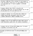
- the method of manufacturing an organic light-emitting diode display panel of the present invention which comprises: S11: depositing a buffer layer 102 on a substrate 101 and arranging an oxide semiconductor pattern layer 103, a gate insulating layer 104, and a gate pattern layer 105 stacked sequentially on the buffer layer 102.
- the step S11 may specifically include: S111: depositing a buffer layer 102 on a substrate 101.
- the buffer layer 102 may be deposited on the substrate 101 by physical vapor deposition method or plasma vapor deposition method, wherein it may deposit a silicon oxide layer on the substrate 101 as a buffer layer 102, or it may be also to deposit a silicon nitride layer on the substrate 101 first, and then depositing a silicon oxide layer with a thickness of not less than 3000 ⁇ on the silicon nitride layer, so that the silicon nitride layer and the silicon oxide layer form a buffer layer 102 collectively.
- the substrate 101 may be a glass substrate, or a silicon substrate, including, but not limited to.
- S112 arranging an oxide semiconductor pattern layer 103 on the buffer layer 102.
- an oxide semiconductor pattern layer 103 on the silicon oxide layer on the buffer layer 102 it may deposit an oxide semiconductor with a thickness of 400 to 600 ⁇ on the silicon oxide layer in the buffer layer 102,and then processing photoresist coating, exposure, development, and peeling of the photolithography process to form an oxide semiconductor pattern layer, because the silicon oxide does not contain hydrogen atoms, in this step S112, the oxide semiconductor pattern layer is not converted into conductor.
- the oxide semiconductor pattern layer 103 comprises a first part 1031 and a second part 1032, the second part 1032 is adjacent to the first part 1031.
- the second part 1032 is located on opposite sides of the first part 1031.
- the oxide semiconductor is indium gallium zinc oxide (IGZO.)
- S113 arranging a gate insulating layer 104, and a gate pattern layer 105 stacked sequentially, on oxide semiconductor pattern layer 103.
- the gate insulating layer 104 is arranged opposite to the first part 1031 of the oxide semiconductor pattern layer 103,the gate insulating layer 104 comprises a third part 1041 and a fourth part 1042, the fourth part 1042 is adjacent to the third part 1041.
- the fourth part 1042 is located on opposite sides of the third part 1041 and the third part 1041 is arranged opposite to the gate pattern layer 105.
- the physical vapor deposition method or plasma vapor deposition method may use the physical vapor deposition method or plasma vapor deposition method to deposit a silicon oxide layer with a thickness of 1000 to 2000 ⁇ on the buffer layer 102,and the silicon oxide layer covers the oxide semiconductor pattern layer 103,and then depositing a metal layer on the silicon oxide layer, after photoresist coating, exposure, and development, etching the metal layer and the silicon oxide layer simultaneously, to form the gate pattern layer 105 and the gate insulating layer 104.
- suitable etching conditions make that the opposite sides of the gate insulating layer 104 extends beyond the gate pattern layer 105.
- the parts of the opposite sides of the gate insulating layer extending beyond the gate pattern layer are the fourth part 1042, and the part in the middle, arranging opposite to the gate pattern layer 105 is the third part 1041.
- the metal layer is molybdenum, aluminum or copper metal layer, including, but not limited to.
- the length of the fourth part 1042 is 0.3 ⁇ m to 1 ⁇ m.
- the gate insulating layer 104 and the gate pattern layer 105 may be formed in two steps, respectively. It may deposit the silicon oxide layer on the buffer layer 102 first, processing photoresist coating, exposure, development, etching, and peeling, to form the gate insulating layer 104 arranged opposite to the oxide semiconductor pattern layer 103. Then depositing metal layer on the gate insulating layer 104, processing photoresist coating, exposure, development, etching, and peeling again, to form the gate pattern layer 105, and make that the gate pattern layer 105 is arranged opposite to the third part 1041 of the gate insulating layer 104.
- the dielectric layer 106 comprises a silicon nitride layer in contact with the oxide semiconductor pattern layer 103.
- the physical vapor deposition method or plasma vapor deposition method may use the physical vapor deposition method or plasma vapor deposition method to deposit a silicon nitride layer with a thickness of 4000 to 5000 ⁇ on the buffer layer 102 to form the dielectric layer 106,or it may deposit a silicon nitride layer with a thickness of 3000 ⁇ on the buffer layer 102, and then deposit a silicon oxide layer with a thickness of 3000 ⁇ , so that the silicon nitride layer and the silicon oxide layer form a dielectric layer 106 collectively.
- the thickness of the silicon nitride layer in the dielectric layer 106 is larger than the thickness of the oxide semiconductor pattern layer 103 and the thickness of the gate insulating layer 104, so that the dielectric layer 106 can contact the second part 1032 of the oxide semiconductor pattern layer 103 and the fourth part 1042 of the gate insulating layer 104.
- the silicon nitride layer contains hydrogen atoms
- the hydrogen atoms are diffused to the oxide semiconductor pattern layer 103 where in the bottom as shown in Fig. 2 .
- the hydrogen atoms diffuse to the second part 1032 so that the second part 1032 is doped with hydrogen atoms to have conductor characteristics.
- the gate insulating layer 104 is a silicon oxide layer
- the first part 1031 arranged opposite the gate insulating layer 104 is protected by the gate insulating layer 104, to prevent the diffusion of hydrogen atoms into the first part 1031, so that after the annealing, the first part 1031 still holds semiconductor characteristics.
- the gate insulating layer 104 is larger in size on the cross-section than the gate pattern layer 105,to further prevent the hydrogen atoms in the silicon nitride layer from diffusing down to the first part 1031, so that the first part 1031 still holds semiconductor characteristics.
- the step S14 may specifically include: S141: arranging a contact hole 1061 connected to a part of the oxide semiconductor pattern layer in the dielectric layer 106.
- a patterned contact hole may be formed by photoresist coating and exposure, then processed dry etching, the contact hole 1061 may be obtained after removal.
- both the dielectric layer 106 and the second part 1032 on both sides of the oxide semiconductor pattern layer 103 have a contact hole 1061.
- it may deposit metal on the dielectric layer 106 and the contact hole 1061 to form a metal layer by physical vapor deposition method, then depositing a photoresist layer on the deposited metal layer, and processing exposure, development, etching, and peeling, to form a patterned source 107 and drain 108. Because the contact hole 1061 is connected to the second part 1032 of the oxide semiconductor pattern layer 103, so that the patterned source 107 and the drain 108 are in contact with the second part 1032 of the oxide semiconductor pattern layer 103.
- the present embodiment further comprises: S15: arranging a flat layer 109 and a pixel defining layer 110 stacked sequentially on the dielectric layer 106.
- it may deposit a silicon nitride layer or a silicon oxide layer on the dielectric layer 106 by physical vapor deposition method or a plasma vapor deposition method, to form the flat layer 109,thendepositing a silicon nitride layer or a silicon oxide layer on the flat layer 109, and processing exposure, development, and, etching, to form a pixel light emitting region.
- the silicon nitride layer or the silicon oxide layer with the pixel light emitting region is the pixel defining layer 110.
- anode layer 1111 arranging sequentially an anode layer 1111, an electron transport layer 1112, a light emitting layer 1113, a hole transport layer 1114, and a cathode layer 1115 at the position opposite to the pixel light emitting region on the pixel definition layer 110.
- the OLED display panel of the embodiment of the present invention which comprises a buffer layer 102 deposited on a substrate 101; an oxide semiconductor pattern layer 103, a gate insulating layer 104, and a gate pattern layer 105 stacked sequentially on the buffer layer 102; a dielectric layer 106 covers the oxide semiconductor pattern layer 103, the gate insulating layer 104, and the gate pattern layer 105; and a source 107 and a drain108 are in contact with the oxide semiconductor pattern layer 103.
- the oxide semiconductor pattern layer 103 comprises a first part 1031 and a second part 1032, the second part 1032 is adjacent to the first part 1031, the first part 1031 is arranged opposite to the gate insulating layer 104, the second part 1032 has conductor characteristics.
- the dielectric layer 106 comprises a silicon nitride layer in contact with the oxide semiconductor pattern layer 103. Because the silicon nitride layer contains hydrogen atoms, during the manufacturing process, the hydrogen atoms in the silicon nitride layer diffuse to the oxide semiconductor pattern layer 103, so as the second part 1032 in contact with the silicon nitride layer, is doped with the hydrogen atoms, thereby the second part 1032 has conductor characteristics.
- the first part 1031 is arrange opposite to the gate insulating layer 104 and is protected by the gate insulating layer 104 to prevent the first part 1031 from doping the hydrogen atoms, so that the first part 1031 still holds semiconductor characteristics.
- the display panel of the present embodiment further comprises a flat layer 109, a pixel defining layer 110, and an OLED device layer 111 stacked sequentially on the dielectric layer 106.
- the present invention is different from the prior art of a buffer layer deposited on a substrate and an oxide semiconductor pattern layer, a gate insulating layer, and a gate pattern layer are stacked sequentially on the buffer layer; arranging a dielectric layer for covering the oxide semiconductor pattern layer, the gate insulating layer, and the gate pattern layer on the buffer layer, and the dielectric layer comprises a silicon nitride layer in contact with the oxide semiconductor pattern layer; annealing the dielectric layer, and the silicon nitride layer making a part of oxide semiconductor pattern layer to have conductor characteristics during the annealing process; a method of arranging a source and a drain are in contact with the part of oxide semiconductor pattern layer, with conductor characteristics, wherein the method is to use the feature that silicon nitride has more hydrogen, so that the oxide semiconductor in contact with the part of oxide semiconductor pattern layer with conductor characteristics, can be continuously doped with hydrogen to hold conductor characteristics, and the contact impedance between the part of oxide semiconductor pattern layer and the source and the drain can be continuously maintained
Landscapes
- Engineering & Computer Science (AREA)
- Microelectronics & Electronic Packaging (AREA)
- Manufacturing & Machinery (AREA)
- Physics & Mathematics (AREA)
- Geometry (AREA)
- Thin Film Transistor (AREA)
- Electroluminescent Light Sources (AREA)
- Devices For Indicating Variable Information By Combining Individual Elements (AREA)
- Formation Of Insulating Films (AREA)
Abstract
Description
- The present invention relates to a technology of display, and more particularly, to an organic light-emitting display panel and a manufacturing method thereof.
- Currently, because oxide semiconductor thin film transistor (TFT)with the top gate structure has a smaller parasitic capacitance, the size of TFT can be smaller to be a better choice for organic light-emitting display (OLED) drive. However, the oxide semiconductor in contact with a source and a drain, need to be processed to be converted into conductor in the manufacturing process of the oxide semiconductor TFT with the top gate structure, thereby the contact impedance of the source and the drain is reduced, and the switching function of the TFT is achieved.
- In the prior art, to convert the oxide semiconductor in contact with the source and the drain into a conductor, is generally processed by hydrogen plasma or argon plasma. However, because the OLED display panel has another annealing process after arranging the TFT, the annealing processes will make the conductive oxide to be converted back into semiconductor, so that the contact impedance of the source and the drain will become larger, the TFT characteristics is reduced, and even the TFT losses its switching function.
- The present invention is mainly to provide an OLED display panel and a manufacturing method thereof, to solve the problem that the contact impedance of source and drain become larger because a part of oxide semiconductor with conductor characteristics is converted into back to semiconductor in the OLED display panel manufacturing process.
- In order to solve the above-mentioned technical problem, a technical solution adopted by the present invention is: providing a method of manufacturing an organic light-emitting diode display panel, wherein the method comprises: depositing a buffer layer on a substrate and arranging an oxide semiconductor pattern layer, a gate insulating layer, and a gate pattern layer stacked sequentially on the buffer layer; arranging a dielectric layer for covering the oxide semiconductor pattern layer, the gate insulating layer, and the gate pattern layer on the buffer layer, and the dielectric layer comprises a silicon nitride layer in contact with the oxide semiconductor pattern layer; annealing the dielectric layer, and the silicon nitride layer making a part of oxide semiconductor pattern layer to have conductor characteristics during the annealing process; arranging a source and a drain in contact with the part of oxide semiconductor pattern layer, with conductor characteristics; wherein the buffer layer comprises a silicon oxide layer in contact with the oxide semiconductor pattern layer; wherein the gate insulating layer comprises a third part and a fourth part, the fourth part is adjacent to the third part, the third part is arranged opposite to the gate pattern layer, the fourth part is in contact with the nitrogen silicon layer.
- In order to solve the above-mentioned technical problem, a further technical solution adopted by the present invention is: providing a method of manufacturing an organic light-emitting diode display panel, wherein the method comprises: depositing a buffer layer on a substrate and arranging an oxide semiconductor pattern layer, a gate insulating layer, and a gate pattern layer stacked sequentially on the buffer layer; arranging a dielectric layer for covering the oxide semiconductor pattern layer, the gate insulating layer, and the gate pattern layer on the buffer layer, and the dielectric layer comprises a silicon nitride layer in contact with the oxide semiconductor pattern layer; annealing the dielectric layer, and the silicon nitride layer making a part of oxide semiconductor pattern layer to have conductor characteristics during the annealing process; arranging a source and a drain are in contact with the part of oxide semiconductor pattern layer, with conductor characteristics.
- In order to solve the above-mentioned technical problem, a further technical solution adopted by the present invention is: providing an organic light-emitting diode display panel, wherein the display panel comprises: depositing a buffer layer on a substrate and arranging an oxide semiconductor pattern layer, a gate insulating layer, and a gate pattern layer stacked sequentially on the buffer layer, wherein a part of oxide semiconductor pattern layer has conductor characteristics; a dielectric layer covers the oxide semiconductor pattern layer, the gate insulating layer, and the gate pattern layer, and the dielectric layer comprises a silicon nitride layer in contact with the oxide semiconductor pattern layer; a source and a drain are in contact with the part of oxide semiconductor pattern layer, with conductor characteristics.
- The present invention can be concluded with the following advantages, the present invention is different from the prior art of a buffer layer deposited on a substrate and an oxide semiconductor pattern layer, a gate insulating layer, and a gate pattern layer are stacked sequentially on the buffer layer; arranging a dielectric layer for covering the oxide semiconductor pattern layer, the gate insulating layer, and the gate pattern layer on the buffer layer, and the dielectric layer comprises a silicon nitride layer in contact with the oxide semiconductor pattern layer; annealing the dielectric layer, and the silicon nitride layer making a part of oxide semiconductor pattern layer to have conductor characteristics during the annealing process; a method of arranging a source and a drain are in contact with the part of oxide semiconductor pattern layer, with conductor characteristics, wherein the method is to use the feature that silicon nitride has more hydrogen atoms, so that the oxide semiconductor in contact with the part of oxide semiconductor pattern layer with conductor characteristics, can be continuously doped with hydrogen atoms to hold conductor characteristics, and the contact impedance between the part of oxide semiconductor pattern layer and the source and the drain can be continuously maintained at a low state to achieve the function of TFT.
-
-
Figure 1 is a flow chart of method of manufacturing an organic light-emitting diode display panel of an embodiment in the present invention; -
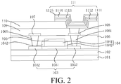
Figure 2 is a structural illustration of an embodiment made in accordance to an organic light-emitting diode display panel in the present invention; -
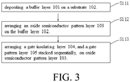
Figure 3 is a specific flow chart of step S11 inFig. 1 ; and -
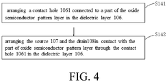
Figure 4 is a specific flow chart of step S14 inFig. 1 . - Technical implementation will be described below clearly and fully by combining with drawings made in accordance with an embodiment in the present invention.
- Referring to
Fig. 1 andFig. 2 , the method of manufacturing an organic light-emitting diode display panel of the present invention, which comprises:
S11: depositing abuffer layer 102 on asubstrate 101 and arranging an oxidesemiconductor pattern layer 103, agate insulating layer 104, and agate pattern layer 105 stacked sequentially on thebuffer layer 102. - Referring to
Fig. 3 , the step S11 may specifically include:
S111: depositing abuffer layer 102 on asubstrate 101. - Specifically, before depositing the
buffer layer 102, cleaning thesubstrate 101,then thebuffer layer 102 may be deposited on thesubstrate 101 by physical vapor deposition method or plasma vapor deposition method, wherein it may deposit a silicon oxide layer on thesubstrate 101 as abuffer layer 102, or it may be also to deposit a silicon nitride layer on thesubstrate 101 first, and then depositing a silicon oxide layer with a thickness of not less than 3000 Å on the silicon nitride layer, so that the silicon nitride layer and the silicon oxide layer form abuffer layer 102 collectively. - Wherein the
substrate 101 may be a glass substrate, or a silicon substrate, including, but not limited to. - S112: arranging an oxide
semiconductor pattern layer 103 on thebuffer layer 102. - Specifically, arranging an oxide
semiconductor pattern layer 103 on the silicon oxide layer on thebuffer layer 102, it may deposit an oxide semiconductor with a thickness of 400 to 600 Å on the silicon oxide layer in thebuffer layer 102,and then processing photoresist coating, exposure, development, and peeling of the photolithography process to form an oxide semiconductor pattern layer, because the silicon oxide does not contain hydrogen atoms, in this step S112, the oxide semiconductor pattern layer is not converted into conductor. - Wherein the oxide
semiconductor pattern layer 103 comprises afirst part 1031 and asecond part 1032, thesecond part 1032 is adjacent to thefirst part 1031. In the figure of the present embodiment, thesecond part 1032 is located on opposite sides of thefirst part 1031. - Preferably, the oxide semiconductor is indium gallium zinc oxide (IGZO.)
- S113: arranging a
gate insulating layer 104, and agate pattern layer 105 stacked sequentially, on oxidesemiconductor pattern layer 103. - Wherein the
gate insulating layer 104 is arranged opposite to thefirst part 1031 of the oxidesemiconductor pattern layer 103,thegate insulating layer 104 comprises a third part 1041 and afourth part 1042, thefourth part 1042 is adjacent to the third part 1041. In the figure of the present embodiment, thefourth part 1042 is located on opposite sides of the third part 1041 and the third part 1041 is arranged opposite to thegate pattern layer 105. - Specifically, it may use the physical vapor deposition method or plasma vapor deposition method to deposit a silicon oxide layer with a thickness of 1000 to 2000 Å on the
buffer layer 102,and the silicon oxide layer covers the oxidesemiconductor pattern layer 103,and then depositing a metal layer on the silicon oxide layer, after photoresist coating, exposure, and development, etching the metal layer and the silicon oxide layer simultaneously, to form thegate pattern layer 105 and thegate insulating layer 104. During the etching process, as shown inFig. 2 , suitable etching conditions make that the opposite sides of thegate insulating layer 104 extends beyond thegate pattern layer 105. The parts of the opposite sides of the gate insulating layer extending beyond the gate pattern layer are thefourth part 1042, and the part in the middle, arranging opposite to thegate pattern layer 105 is the third part 1041. - Wherein the metal layer is molybdenum, aluminum or copper metal layer, including, but not limited to.
- Preferably, the length of the
fourth part 1042 is 0.3 µm to 1 µm. - In other embodiments, the
gate insulating layer 104 and thegate pattern layer 105 may be formed in two steps, respectively. It may deposit the silicon oxide layer on thebuffer layer 102 first, processing photoresist coating, exposure, development, etching, and peeling, to form thegate insulating layer 104 arranged opposite to the oxidesemiconductor pattern layer 103. Then depositing metal layer on thegate insulating layer 104, processing photoresist coating, exposure, development, etching, and peeling again, to form thegate pattern layer 105, and make that thegate pattern layer 105 is arranged opposite to the third part 1041 of thegate insulating layer 104. - S12: arranging a
dielectric layer 106 for covering the oxidesemiconductor pattern layer 103, thegate insulating layer 104, and thegate pattern layer 105 on thebuffer layer 102. - Wherein the
dielectric layer 106 comprises a silicon nitride layer in contact with the oxidesemiconductor pattern layer 103. - Specifically, it may use the physical vapor deposition method or plasma vapor deposition method to deposit a silicon nitride layer with a thickness of 4000 to 5000 Å on the
buffer layer 102 to form thedielectric layer 106,or it may deposit a silicon nitride layer with a thickness of 3000 Å on thebuffer layer 102, and then deposit a silicon oxide layer with a thickness of 3000 Å, so that the silicon nitride layer and the silicon oxide layer form adielectric layer 106 collectively. It should be notice that by the above-mentioned steps, the thickness of the silicon nitride layer in thedielectric layer 106 is larger than the thickness of the oxidesemiconductor pattern layer 103 and the thickness of thegate insulating layer 104, so that thedielectric layer 106 can contact thesecond part 1032 of the oxidesemiconductor pattern layer 103 and thefourth part 1042 of thegate insulating layer 104. - S13: annealing the
dielectric layer 106, and the silicon nitride layer making a part of oxide semiconductor pattern layer to have conductor characteristics during the annealing process. - Specifically, because the silicon nitride layer contains hydrogen atoms, during the annealing process of the
dielectric layer 106, under high temperature, the hydrogen atoms are diffused to the oxidesemiconductor pattern layer 103 where in the bottom as shown inFig. 2 . During the diffusion process, because thesecond part 1032 of the oxidesemiconductor pattern layer 103 is in contact with the silicon nitride layer, the hydrogen atoms diffuse to thesecond part 1032 so that thesecond part 1032 is doped with hydrogen atoms to have conductor characteristics. - Wherein, because the
gate insulating layer 104 is a silicon oxide layer, thefirst part 1031 arranged opposite thegate insulating layer 104 is protected by thegate insulating layer 104, to prevent the diffusion of hydrogen atoms into thefirst part 1031, so that after the annealing, thefirst part 1031 still holds semiconductor characteristics. And according to the above-described step S113, thegate insulating layer 104 is larger in size on the cross-section than thegate pattern layer 105,to further prevent the hydrogen atoms in the silicon nitride layer from diffusing down to thefirst part 1031, so that thefirst part 1031 still holds semiconductor characteristics. - S14: arranging a
source 107 and adrain 108 in contact with the part of oxide semiconductor pattern layer, with conductor characteristics. - Referring to
Fig. 4 , the step S14 may specifically include:
S141: arranging acontact hole 1061 connected to a part of the oxide semiconductor pattern layer in thedielectric layer 106. - Specifically, a patterned contact hole may be formed by photoresist coating and exposure, then processed dry etching, the
contact hole 1061 may be obtained after removal. - Wherein both the
dielectric layer 106 and thesecond part 1032 on both sides of the oxidesemiconductor pattern layer 103, have acontact hole 1061. - S142: arranging the
source 107 and thedrain 108 in contact with the part of oxide semiconductor pattern layer through thecontact hole 1061 in thedielectric layer 106. - Specifically, it may deposit metal on the
dielectric layer 106 and thecontact hole 1061 to form a metal layer by physical vapor deposition method, then depositing a photoresist layer on the deposited metal layer, and processing exposure, development, etching, and peeling, to form a patternedsource 107 anddrain 108. Because thecontact hole 1061 is connected to thesecond part 1032 of the oxidesemiconductor pattern layer 103, so that thepatterned source 107 and thedrain 108 are in contact with thesecond part 1032 of the oxidesemiconductor pattern layer 103. - Further, the present embodiment further comprises:
S15: arranging aflat layer 109 and apixel defining layer 110 stacked sequentially on thedielectric layer 106. - Specifically, it may deposit a silicon nitride layer or a silicon oxide layer on the
dielectric layer 106 by physical vapor deposition method or a plasma vapor deposition method, to form theflat layer 109,thendepositing a silicon nitride layer or a silicon oxide layer on theflat layer 109, and processing exposure, development, and, etching, to form a pixel light emitting region. The silicon nitride layer or the silicon oxide layer with the pixel light emitting region is thepixel defining layer 110. - S16: arranging an
OLED device layer 111 on thepixel defining layer 110. - Specifically, arranging sequentially an
anode layer 1111, anelectron transport layer 1112, alight emitting layer 1113, ahole transport layer 1114, and acathode layer 1115 at the position opposite to the pixel light emitting region on thepixel definition layer 110. - Further, referring to
Fig. 2 , the OLED display panel of the embodiment of the present invention, which comprises abuffer layer 102 deposited on asubstrate 101; an oxidesemiconductor pattern layer 103, agate insulating layer 104, and agate pattern layer 105 stacked sequentially on thebuffer layer 102; adielectric layer 106 covers the oxidesemiconductor pattern layer 103, thegate insulating layer 104, and thegate pattern layer 105; and asource 107 and a drain108 are in contact with the oxidesemiconductor pattern layer 103. - Wherein the oxide
semiconductor pattern layer 103 comprises afirst part 1031 and asecond part 1032, thesecond part 1032 is adjacent to thefirst part 1031, thefirst part 1031 is arranged opposite to thegate insulating layer 104, thesecond part 1032 has conductor characteristics. - Specifically, the
dielectric layer 106 comprises a silicon nitride layer in contact with the oxidesemiconductor pattern layer 103. Because the silicon nitride layer contains hydrogen atoms, during the manufacturing process, the hydrogen atoms in the silicon nitride layer diffuse to the oxidesemiconductor pattern layer 103, so as thesecond part 1032 in contact with the silicon nitride layer, is doped with the hydrogen atoms, thereby thesecond part 1032 has conductor characteristics. Thefirst part 1031 is arrange opposite to thegate insulating layer 104 and is protected by thegate insulating layer 104 to prevent thefirst part 1031 from doping the hydrogen atoms, so that thefirst part 1031 still holds semiconductor characteristics. - Further, the display panel of the present embodiment further comprises a
flat layer 109, apixel defining layer 110, and anOLED device layer 111 stacked sequentially on thedielectric layer 106. - Each of the layers in the present embodiment can be manufactured by the steps corresponding to the above-described methods, therefore no additional description is given here below.
- The present invention is different from the prior art of a buffer layer deposited on a substrate and an oxide semiconductor pattern layer, a gate insulating layer, and a gate pattern layer are stacked sequentially on the buffer layer; arranging a dielectric layer for covering the oxide semiconductor pattern layer, the gate insulating layer, and the gate pattern layer on the buffer layer, and the dielectric layer comprises a silicon nitride layer in contact with the oxide semiconductor pattern layer; annealing the dielectric layer, and the silicon nitride layer making a part of oxide semiconductor pattern layer to have conductor characteristics during the annealing process; a method of arranging a source and a drain are in contact with the part of oxide semiconductor pattern layer, with conductor characteristics, wherein the method is to use the feature that silicon nitride has more hydrogen, so that the oxide semiconductor in contact with the part of oxide semiconductor pattern layer with conductor characteristics, can be continuously doped with hydrogen to hold conductor characteristics, and the contact impedance between the part of oxide semiconductor pattern layer and the source and the drain can be continuously maintained at a low state to achieve the function of TFT.
- Embodiments of the present invention have been described, but not intending to impose any unduly constraint to the appended claims. Any modification of equivalent structure or equivalent process made according to the disclosure and drawings of the present invention, or any application thereof, directly or indirectly, to other related fields of technique, is considered encompassed in the scope of protection defined by the clams of the present invention.
Claims (15)
- A method of manufacturing an organic light-emitting diode display panel, wherein the method comprises:depositing a buffer layer on a substrate and arranging an oxide semiconductor pattern layer, a gate insulating layer, and a gate pattern layer stacked sequentially on the buffer layer;arranging a dielectric layer for covering the oxide semiconductor pattern layer, the gate insulating layer, and the gate pattern layer on the buffer layer, and the dielectric layer comprising a silicon nitride layer in contact with the oxide semiconductor pattern layer;annealing the dielectric layer, and the silicon nitride layer making a part of oxide semiconductor pattern layer to have conductor characteristics during the annealing process;arranging a source and a drain in contact with the part of oxide semiconductor pattern layer, with conductor characteristics;wherein the buffer layer comprises a silicon oxide layer in contact with the oxide semiconductor pattern layer;wherein the gate insulating layer comprises a third part and a fourth part, the fourth part is adjacent to the third part, the third part is arranged opposite to the gate pattern layer, the fourth part is in contact with the nitrogen silicon layer.
- The method as recited in claim 1, wherein the oxide semiconductor pattern layer comprises a first part and a second part, the second part is adjacent to the first part, the first part is arranged opposite to the gate insulating layer, the second part is in contact with the silicon nitride layer, and the above-mentioned description of annealing the dielectric layer, and the silicon nitride layer making a part of oxide semiconductor pattern layer to have conductor characteristics during the annealing process, which comprises:
annealing the dielectric layer, and the silicon nitride layer making the second part in contact with the silicon nitride layer to have conductor characteristics during the annealing process. - The method as recited in claim 2, wherein the silicon nitride layer contains hydrogen atoms, above-mentioned description of annealing the dielectric layer, and the silicon nitride layer making the second part in contact with the silicon nitride layer to have conductor characteristics during the annealing process, which comprises:
during the annealing process, the hydrogen atoms in the silicon nitride layer diffusing to the oxide semiconductor pattern layer, so as the second part in contact with the silicon nitride layer, doped with the hydrogen atoms, thereby having conductor characteristics. - The method as recited in claim 3, wherein the gate insulating layer is a silicon oxide layer, the gate insulating layer and the first part arranged opposite to the gate insulating layer hold semiconductor characteristics after annealing.
- The method as recited in claim 1, wherein the above-mentioned description of arranging a source and a drain in contact with the part of oxide semiconductor pattern layer, with conductor characteristics, which comprises:arranging a contact hole connected to a part of the oxide semiconductor pattern layer in the dielectric layer;arranging the source and the drain in contact with the part of oxide semiconductor pattern layer through the contact hole in the dielectric layer.
- A method of manufacturing an organic light-emitting diode display panel, wherein the method comprises:depositing a buffer layer on a substrate and arranging an oxide semiconductor pattern layer, a gate insulating layer, and a gate pattern layer stacked sequentially on the buffer layer;arranging a dielectric layer for covering the oxide semiconductor pattern layer, the gate insulating layer, and the gate pattern layer on the buffer layer, and the dielectric layer comprising a silicon nitride layer in contact with the oxide semiconductor pattern layer;annealing the dielectric layer, and the silicon nitride layer making a part of oxide semiconductor pattern layer to have conductor characteristics during the annealing process;arranging a source and a drain in contact with the part of oxide semiconductor pattern layer, with conductor characteristics.
- The method as recited in claim 6, wherein the oxide semiconductor pattern layer comprises a first part and a second part, the second part is adjacent to the first part, the first part is arranged opposite to the gate insulating layer, the second part is in contact with the silicon nitride layer, and the above-mentioned description of annealing the dielectric layer, and the silicon nitride layer making a part of oxide semiconductor pattern layer to have conductor characteristics during the annealing process, which comprises:
annealing the dielectric layer, and the silicon nitride layer making the second part in contact with the silicon nitride layer to have conductor characteristics during the annealing process. - The method as recited in claim 2, wherein the silicon nitride layer contains hydrogen atoms, above-mentioned description of annealing the dielectric layer, and the silicon nitride layer making the second part in contact with the silicon nitride layer to have conductor characteristics during the annealing process, which comprises:
during the annealing process, the hydrogen atoms in the silicon nitride layer diffusing to the oxide semiconductor pattern layer, so as the second part in contact with the silicon nitride layer, doped with the hydrogen atoms, thereby having conductor characteristics. - The method as recited in claim 8, wherein the gate insulating layer is a silicon oxide layer, the gate insulating layer and the first part arranged opposite to the gate insulating layer hold semiconductor characteristics after annealing.
- The method as recited in claim 6, wherein the buffer layer comprises a silicon oxide layer in contact with the oxide semiconductor pattern layer;
- The method as recited in claim 6, wherein the gate insulating layer comprises a third part and a fourth part, the fourth part is adjacent to the third part, the third part is arranged opposite to the gate pattern layer, the fourth part is in contact with the nitrogen silicon layer.
- The method as recited in claim 6, wherein the above-mentioned description of arranging a source and a drain in contact with the part of oxide semiconductor pattern layer, with conductor characteristics, which comprises:arranging a contact hole connected to a part of the oxide semiconductor pattern layer in the dielectric layer;arranging the source and the drain in contact with the part of oxide semiconductor pattern layer through the contact hole in the dielectric layer.
- An organic light-emitting diode display panel, wherein the display panel comprises:depositing a buffer layer on a substrate and arranging an oxide semiconductor pattern layer, a gate insulating layer, and a gate pattern layer stacked sequentially on the buffer layer, wherein a part of oxide semiconductor pattern layer has conductor characteristics;a dielectric layer covering the oxide semiconductor pattern layer, the gate insulating layer, and the gate pattern layer, and the dielectric layer comprising a silicon nitride layer in contact with the oxide semiconductor pattern layer;a source and a drain in contact with the part of oxide semiconductor pattern layer, with conductor characteristics.
- The display panel as recited in claim 13, wherein the oxide semiconductor pattern layer comprises a first part and a second part, the second part is adjacent to the first part, the first part is arranged opposite to the gate insulating layer, the second part is in contact with the silicon nitride layer, thereby the second part has conductor characteristics.
- The display panel as recited in claim 14, wherein the silicon nitride layer contains hydrogen atoms, during the manufacturing process, the hydrogen atoms in the silicon nitride layer diffuse to the oxide semiconductor pattern layer, so as the second part in contact with the silicon nitride layer, is doped with the hydrogen atoms, thereby the second part has conductor characteristics.
Applications Claiming Priority (2)
| Application Number | Priority Date | Filing Date | Title |
|---|---|---|---|
| CN201710302087.1A CN107195583B (en) | 2017-05-02 | 2017-05-02 | A kind of OLED display panel and preparation method thereof |
| PCT/CN2017/086234 WO2018201542A1 (en) | 2017-05-02 | 2017-05-27 | Oled display panel and method for manufacturing same |
Publications (3)
| Publication Number | Publication Date |
|---|---|
| EP3621105A1 true EP3621105A1 (en) | 2020-03-11 |
| EP3621105A4 EP3621105A4 (en) | 2021-01-13 |
| EP3621105B1 EP3621105B1 (en) | 2025-12-10 |
Family
ID=59873702
Family Applications (1)
| Application Number | Title | Priority Date | Filing Date |
|---|---|---|---|
| EP17908502.2A Active EP3621105B1 (en) | 2017-05-02 | 2017-05-27 | Oled display panel and method for manufacturing same |
Country Status (6)
| Country | Link |
|---|---|
| US (1) | US20180323246A1 (en) |
| EP (1) | EP3621105B1 (en) |
| JP (1) | JP2020520557A (en) |
| KR (1) | KR20200003143A (en) |
| CN (1) | CN107195583B (en) |
| WO (1) | WO2018201542A1 (en) |
Families Citing this family (7)
| Publication number | Priority date | Publication date | Assignee | Title |
|---|---|---|---|---|
| CN109616444B (en) * | 2018-12-03 | 2020-04-10 | 武汉华星光电半导体显示技术有限公司 | TFT substrate manufacturing method and TFT substrate |
| KR102980973B1 (en) | 2019-07-04 | 2026-06-23 | 엘지디스플레이 주식회사 | Display apparatus having an oxide semiconductor pattern |
| CN112186004A (en) * | 2019-07-04 | 2021-01-05 | 乐金显示有限公司 | Display device |
| CN110993610A (en) * | 2019-11-26 | 2020-04-10 | 深圳市华星光电半导体显示技术有限公司 | Array substrate, preparation method thereof and display panel |
| US12418655B2 (en) | 2019-12-16 | 2025-09-16 | Hyundai Motor Company | Decoding device and method for predicting block partitioned into random shape |
| CN113097289A (en) * | 2021-03-30 | 2021-07-09 | 合肥维信诺科技有限公司 | Thin film transistor, preparation method thereof and array substrate |
| KR102605949B1 (en) | 2021-11-09 | 2023-11-24 | 서영대학교 산학협력단 | Alternating current power generator for vehicle |
Family Cites Families (22)
| Publication number | Priority date | Publication date | Assignee | Title |
|---|---|---|---|---|
| US7669390B2 (en) * | 2004-03-08 | 2010-03-02 | Medical Instill Technologies, Inc. | Method for molding and assembling containers with stoppers and filling same |
| JP4365364B2 (en) * | 2004-10-12 | 2009-11-18 | エルジー ディスプレイ カンパニー リミテッド | Organic electroluminescent device and manufacturing method thereof |
| JP5110803B2 (en) * | 2006-03-17 | 2012-12-26 | キヤノン株式会社 | FIELD EFFECT TRANSISTOR USING OXIDE FILM FOR CHANNEL AND METHOD FOR MANUFACTURING THE SAME |
| KR100776498B1 (en) * | 2006-06-09 | 2007-11-16 | 삼성에스디아이 주식회사 | Organic electroluminescent display and manufacturing method thereof |
| KR100889626B1 (en) * | 2007-08-22 | 2009-03-20 | 삼성모바일디스플레이주식회사 | Thin film transistor, manufacturing method thereof, organic light emitting display device having same, and manufacturing method thereof |
| JP5704790B2 (en) * | 2008-05-07 | 2015-04-22 | キヤノン株式会社 | Thin film transistor and display device |
| JP2012015436A (en) * | 2010-07-05 | 2012-01-19 | Sony Corp | Thin film transistor and display device |
| KR20120019017A (en) * | 2010-08-24 | 2012-03-06 | 삼성모바일디스플레이주식회사 | Organic electroluminescence emitting display device and manufacturing method of the same |
| KR101809661B1 (en) * | 2011-06-03 | 2017-12-18 | 삼성디스플레이 주식회사 | Thin film transistor, manufacturing method of thin film transistor, and organic light emitting diode display including the same |
| US8916424B2 (en) * | 2012-02-07 | 2014-12-23 | Semiconductor Energy Laboratory Co., Ltd. | Method for manufacturing semiconductor device |
| TWI596778B (en) * | 2012-06-29 | 2017-08-21 | 半導體能源研究所股份有限公司 | Semiconductor device and method of manufacturing semiconductor device |
| KR102091444B1 (en) * | 2013-10-08 | 2020-03-23 | 삼성디스플레이 주식회사 | Display substrate and method of manufacturing a display substrate |
| CN104576682B (en) * | 2013-10-18 | 2018-03-06 | 昆山工研院新型平板显示技术中心有限公司 | A kind of organic light-emitting display device and preparation method thereof |
| JP2015108731A (en) * | 2013-12-05 | 2015-06-11 | ソニー株式会社 | Semiconductor device and manufacturing method thereof, and display device and electronic apparatus |
| US9443876B2 (en) * | 2014-02-05 | 2016-09-13 | Semiconductor Energy Laboratory Co., Ltd. | Semiconductor device, display device including the semiconductor device, display module including the display device, and electronic device including the semiconductor device, the display device, and the display module |
| CN103887324A (en) * | 2014-04-14 | 2014-06-25 | 友达光电股份有限公司 | An active matrix organic light emitting diode display device integrating a touch panel |
| US10002971B2 (en) * | 2014-07-03 | 2018-06-19 | Semiconductor Energy Laboratory Co., Ltd. | Semiconductor device and display device including the semiconductor device |
| JP6333377B2 (en) * | 2014-07-16 | 2018-05-30 | 株式会社Joled | Transistor, display device and electronic device |
| JP6425508B2 (en) * | 2014-11-25 | 2018-11-21 | 株式会社ジャパンディスプレイ | Thin film transistor |
| US10338446B2 (en) * | 2014-12-16 | 2019-07-02 | Sharp Kabushiki Kaisha | Semiconductor device having low resistance source and drain regions |
| KR20160114511A (en) * | 2015-03-24 | 2016-10-05 | 가부시키가이샤 한도오따이 에네루기 켄큐쇼 | Method for manufacturing semiconductor device |
| JP2017076788A (en) * | 2015-10-12 | 2017-04-20 | 株式会社半導体エネルギー研究所 | Method for manufacturing semiconductor device |
-
2017
- 2017-05-02 CN CN201710302087.1A patent/CN107195583B/en active Active
- 2017-05-27 JP JP2019560294A patent/JP2020520557A/en active Pending
- 2017-05-27 WO PCT/CN2017/086234 patent/WO2018201542A1/en not_active Ceased
- 2017-05-27 EP EP17908502.2A patent/EP3621105B1/en active Active
- 2017-05-27 KR KR1020197035592A patent/KR20200003143A/en not_active Ceased
- 2017-05-27 US US15/541,746 patent/US20180323246A1/en not_active Abandoned
Also Published As
| Publication number | Publication date |
|---|---|
| KR20200003143A (en) | 2020-01-08 |
| CN107195583B (en) | 2019-08-02 |
| EP3621105B1 (en) | 2025-12-10 |
| WO2018201542A1 (en) | 2018-11-08 |
| CN107195583A (en) | 2017-09-22 |
| EP3621105A4 (en) | 2021-01-13 |
| JP2020520557A (en) | 2020-07-09 |
| US20180323246A1 (en) | 2018-11-08 |
Similar Documents
| Publication | Publication Date | Title |
|---|---|---|
| US8759832B2 (en) | Semiconductor device and electroluminescent device and method of making the same | |
| EP3621105B1 (en) | Oled display panel and method for manufacturing same | |
| US9960189B2 (en) | Thin film transistor and manufacturing method thereof, array substrate and display device | |
| US10283529B2 (en) | Method of manufacturing thin-film transistor, thin-film transistor substrate, and flat panel display apparatus | |
| US10153304B2 (en) | Thin film transistors, arrays substrates, and manufacturing methods | |
| US10615266B2 (en) | Thin-film transistor, manufacturing method thereof, and array substrate | |
| US9202896B2 (en) | TFT, method of manufacturing the TFT, and method of manufacturing organic light emitting display device including the TFT | |
| US8633479B2 (en) | Display device with metal oxidel layer and method for manufacturing the same | |
| US8609460B2 (en) | Semiconductor structure and fabricating method thereof | |
| US10777581B2 (en) | Method for manufacturing IGZO thin-film transistor | |
| US9704998B2 (en) | Thin film transistor and method of manufacturing the same, display substrate, and display apparatus | |
| WO2018149171A1 (en) | Array substrate and manufacturing method thereof, and display device | |
| KR20130121655A (en) | Display device, array substrate, thin film transistor and method for manufacturing the same | |
| US11925064B2 (en) | Manufacturing method of display substrate and display device | |
| US11355571B2 (en) | OLED display panel having storage capacitor and manufacturing method thereof | |
| WO2019184252A1 (en) | Flexible tft substrate and manufacturing method thereof | |
| US8710503B2 (en) | Organic light-emitting display and method of manufacturing the same | |
| US9252284B2 (en) | Display substrate and method of manufacturing a display substrate | |
| CN109148535B (en) | Array substrate, manufacturing method thereof and display panel | |
| EP3605613A1 (en) | Manufacturing method of tft panel, and tft panel | |
| KR20110080118A (en) | A thin film transistor having a multilayer etch stop layer and a method of manufacturing the same | |
| US10115745B2 (en) | TFT array substrate and method of forming the same | |
| US11088229B1 (en) | Pixel driving circuit and manufacturing method thereof | |
| US10153308B1 (en) | Manufacturing method for thin film transistor and array substrate |
Legal Events
| Date | Code | Title | Description |
|---|---|---|---|
| STAA | Information on the status of an ep patent application or granted ep patent |
Free format text: STATUS: THE INTERNATIONAL PUBLICATION HAS BEEN MADE |
|
| PUAI | Public reference made under article 153(3) epc to a published international application that has entered the european phase |
Free format text: ORIGINAL CODE: 0009012 |
|
| STAA | Information on the status of an ep patent application or granted ep patent |
Free format text: STATUS: REQUEST FOR EXAMINATION WAS MADE |
|
| 17P | Request for examination filed |
Effective date: 20191128 |
|
| AK | Designated contracting states |
Kind code of ref document: A1 Designated state(s): AL AT BE BG CH CY CZ DE DK EE ES FI FR GB GR HR HU IE IS IT LI LT LU LV MC MK MT NL NO PL PT RO RS SE SI SK SM TR |
|
| AX | Request for extension of the european patent |
Extension state: BA ME |
|
| DAV | Request for validation of the european patent (deleted) | ||
| DAX | Request for extension of the european patent (deleted) | ||
| REG | Reference to a national code |
Ref country code: DE Ref legal event code: R079 Free format text: PREVIOUS MAIN CLASS: H01L0021770000 Ipc: H01L0027320000 |
|
| A4 | Supplementary search report drawn up and despatched |
Effective date: 20201216 |
|
| RIC1 | Information provided on ipc code assigned before grant |
Ipc: H01L 29/66 20060101ALI20201210BHEP Ipc: H01L 27/32 20060101AFI20201210BHEP Ipc: H01L 29/786 20060101ALI20201210BHEP Ipc: H01L 27/12 20060101ALI20201210BHEP |
|
| STAA | Information on the status of an ep patent application or granted ep patent |
Free format text: STATUS: EXAMINATION IS IN PROGRESS |
|
| 17Q | First examination report despatched |
Effective date: 20230907 |
|
| REG | Reference to a national code |
Ref country code: DE Ref legal event code: R079 Free format text: PREVIOUS MAIN CLASS: H01L0027320000 Ipc: H10K0059120000 Ref country code: DE Ref legal event code: R079 Ref document number: 602017093129 Country of ref document: DE Free format text: PREVIOUS MAIN CLASS: H01L0027320000 Ipc: H10K0059120000 |
|
| GRAP | Despatch of communication of intention to grant a patent |
Free format text: ORIGINAL CODE: EPIDOSNIGR1 |
|
| STAA | Information on the status of an ep patent application or granted ep patent |
Free format text: STATUS: GRANT OF PATENT IS INTENDED |
|
| RIC1 | Information provided on ipc code assigned before grant |
Ipc: H10K 59/12 20230101AFI20250623BHEP Ipc: H10D 30/67 20250101ALI20250623BHEP Ipc: H10D 86/40 20250101ALI20250623BHEP Ipc: H10D 86/60 20250101ALI20250623BHEP |
|
| INTG | Intention to grant announced |
Effective date: 20250710 |
|
| GRAS | Grant fee paid |
Free format text: ORIGINAL CODE: EPIDOSNIGR3 |
|
| GRAA | (expected) grant |
Free format text: ORIGINAL CODE: 0009210 |
|
| STAA | Information on the status of an ep patent application or granted ep patent |
Free format text: STATUS: THE PATENT HAS BEEN GRANTED |
|
| AK | Designated contracting states |
Kind code of ref document: B1 Designated state(s): AL AT BE BG CH CY CZ DE DK EE ES FI FR GB GR HR HU IE IS IT LI LT LU LV MC MK MT NL NO PL PT RO RS SE SI SK SM TR |
|
| P01 | Opt-out of the competence of the unified patent court (upc) registered |
Free format text: CASE NUMBER: UPC_APP_0012241_3621105/2025 Effective date: 20251105 |
|
| REG | Reference to a national code |
Ref country code: CH Ref legal event code: F10 Free format text: ST27 STATUS EVENT CODE: U-0-0-F10-F00 (AS PROVIDED BY THE NATIONAL OFFICE) Effective date: 20251210 Ref country code: GB Ref legal event code: FG4D |
|
| REG | Reference to a national code |
Ref country code: DE Ref legal event code: R096 Ref document number: 602017093129 Country of ref document: DE |
|
| REG | Reference to a national code |
Ref country code: IE Ref legal event code: FG4D |
|
| PG25 | Lapsed in a contracting state [announced via postgrant information from national office to epo] |
Ref country code: ES Free format text: LAPSE BECAUSE OF FAILURE TO SUBMIT A TRANSLATION OF THE DESCRIPTION OR TO PAY THE FEE WITHIN THE PRESCRIBED TIME-LIMIT Effective date: 20251210 |
|
| REG | Reference to a national code |
Ref country code: LT Ref legal event code: MG9D |
|
| PG25 | Lapsed in a contracting state [announced via postgrant information from national office to epo] |
Ref country code: NO Free format text: LAPSE BECAUSE OF FAILURE TO SUBMIT A TRANSLATION OF THE DESCRIPTION OR TO PAY THE FEE WITHIN THE PRESCRIBED TIME-LIMIT Effective date: 20260310 |
|
| PG25 | Lapsed in a contracting state [announced via postgrant information from national office to epo] |
Ref country code: FI Free format text: LAPSE BECAUSE OF FAILURE TO SUBMIT A TRANSLATION OF THE DESCRIPTION OR TO PAY THE FEE WITHIN THE PRESCRIBED TIME-LIMIT Effective date: 20251210 Ref country code: HR Free format text: LAPSE BECAUSE OF FAILURE TO SUBMIT A TRANSLATION OF THE DESCRIPTION OR TO PAY THE FEE WITHIN THE PRESCRIBED TIME-LIMIT Effective date: 20251210 |
|
| REG | Reference to a national code |
Ref country code: NL Ref legal event code: MP Effective date: 20251210 |
|
| PG25 | Lapsed in a contracting state [announced via postgrant information from national office to epo] |
Ref country code: RS Free format text: LAPSE BECAUSE OF FAILURE TO SUBMIT A TRANSLATION OF THE DESCRIPTION OR TO PAY THE FEE WITHIN THE PRESCRIBED TIME-LIMIT Effective date: 20260310 |
|
| PG25 | Lapsed in a contracting state [announced via postgrant information from national office to epo] |
Ref country code: LV Free format text: LAPSE BECAUSE OF FAILURE TO SUBMIT A TRANSLATION OF THE DESCRIPTION OR TO PAY THE FEE WITHIN THE PRESCRIBED TIME-LIMIT Effective date: 20251210 |
|
| PG25 | Lapsed in a contracting state [announced via postgrant information from national office to epo] |
Ref country code: BG Free format text: LAPSE BECAUSE OF FAILURE TO SUBMIT A TRANSLATION OF THE DESCRIPTION OR TO PAY THE FEE WITHIN THE PRESCRIBED TIME-LIMIT Effective date: 20251210 |
|
| REG | Reference to a national code |
Ref country code: AT Ref legal event code: MK05 Ref document number: 1867568 Country of ref document: AT Kind code of ref document: T Effective date: 20251210 |
|
| PG25 | Lapsed in a contracting state [announced via postgrant information from national office to epo] |
Ref country code: NL Free format text: LAPSE BECAUSE OF FAILURE TO SUBMIT A TRANSLATION OF THE DESCRIPTION OR TO PAY THE FEE WITHIN THE PRESCRIBED TIME-LIMIT Effective date: 20251210 |
|
| PG25 | Lapsed in a contracting state [announced via postgrant information from national office to epo] |
Ref country code: LT Free format text: LAPSE BECAUSE OF FAILURE TO SUBMIT A TRANSLATION OF THE DESCRIPTION OR TO PAY THE FEE WITHIN THE PRESCRIBED TIME-LIMIT Effective date: 20251210 |
|
| PG25 | Lapsed in a contracting state [announced via postgrant information from national office to epo] |
Ref country code: SM Free format text: LAPSE BECAUSE OF FAILURE TO SUBMIT A TRANSLATION OF THE DESCRIPTION OR TO PAY THE FEE WITHIN THE PRESCRIBED TIME-LIMIT Effective date: 20251210 |
|
| PG25 | Lapsed in a contracting state [announced via postgrant information from national office to epo] |
Ref country code: PL Free format text: LAPSE BECAUSE OF FAILURE TO SUBMIT A TRANSLATION OF THE DESCRIPTION OR TO PAY THE FEE WITHIN THE PRESCRIBED TIME-LIMIT Effective date: 20251210 |
|
| PG25 | Lapsed in a contracting state [announced via postgrant information from national office to epo] |
Ref country code: IT Free format text: LAPSE BECAUSE OF FAILURE TO SUBMIT A TRANSLATION OF THE DESCRIPTION OR TO PAY THE FEE WITHIN THE PRESCRIBED TIME-LIMIT Effective date: 20251210 |
|
| PGFP | Annual fee paid to national office [announced via postgrant information from national office to epo] |
Ref country code: DE Payment date: 20260512 Year of fee payment: 10 |
|
| PG25 | Lapsed in a contracting state [announced via postgrant information from national office to epo] |
Ref country code: AT Free format text: LAPSE BECAUSE OF FAILURE TO SUBMIT A TRANSLATION OF THE DESCRIPTION OR TO PAY THE FEE WITHIN THE PRESCRIBED TIME-LIMIT Effective date: 20251210 |
|
| PG25 | Lapsed in a contracting state [announced via postgrant information from national office to epo] |
Ref country code: EE Free format text: LAPSE BECAUSE OF FAILURE TO SUBMIT A TRANSLATION OF THE DESCRIPTION OR TO PAY THE FEE WITHIN THE PRESCRIBED TIME-LIMIT Effective date: 20251210 |
|
| PG25 | Lapsed in a contracting state [announced via postgrant information from national office to epo] |
Ref country code: IS Free format text: LAPSE BECAUSE OF FAILURE TO SUBMIT A TRANSLATION OF THE DESCRIPTION OR TO PAY THE FEE WITHIN THE PRESCRIBED TIME-LIMIT Effective date: 20260410 Ref country code: PT Free format text: LAPSE BECAUSE OF FAILURE TO SUBMIT A TRANSLATION OF THE DESCRIPTION OR TO PAY THE FEE WITHIN THE PRESCRIBED TIME-LIMIT Effective date: 20260410 |
|
| PG25 | Lapsed in a contracting state [announced via postgrant information from national office to epo] |
Ref country code: CZ Free format text: LAPSE BECAUSE OF FAILURE TO SUBMIT A TRANSLATION OF THE DESCRIPTION OR TO PAY THE FEE WITHIN THE PRESCRIBED TIME-LIMIT Effective date: 20251210 |
|
| PG25 | Lapsed in a contracting state [announced via postgrant information from national office to epo] |
Ref country code: SK Free format text: LAPSE BECAUSE OF FAILURE TO SUBMIT A TRANSLATION OF THE DESCRIPTION OR TO PAY THE FEE WITHIN THE PRESCRIBED TIME-LIMIT Effective date: 20251210 |
|
| PG25 | Lapsed in a contracting state [announced via postgrant information from national office to epo] |
Ref country code: SE Free format text: LAPSE BECAUSE OF FAILURE TO SUBMIT A TRANSLATION OF THE DESCRIPTION OR TO PAY THE FEE WITHIN THE PRESCRIBED TIME-LIMIT Effective date: 20251210 |