EP3621103A2 - Component carrier with a photoimagable dielectric layer and a structured conductive layer being used as a mask for selectively exposing the photoimagable dielectric layer with electromagnetic radiation - Google Patents
Component carrier with a photoimagable dielectric layer and a structured conductive layer being used as a mask for selectively exposing the photoimagable dielectric layer with electromagnetic radiation Download PDFInfo
- Publication number
- EP3621103A2 EP3621103A2 EP19193661.6A EP19193661A EP3621103A2 EP 3621103 A2 EP3621103 A2 EP 3621103A2 EP 19193661 A EP19193661 A EP 19193661A EP 3621103 A2 EP3621103 A2 EP 3621103A2
- Authority
- EP
- European Patent Office
- Prior art keywords
- layer structure
- component carrier
- electrically conductive
- dielectric layer
- photoimagable dielectric
- Prior art date
- Legal status (The legal status is an assumption and is not a legal conclusion. Google has not performed a legal analysis and makes no representation as to the accuracy of the status listed.)
- Granted
Links
Images



Classifications
-
- H—ELECTRICITY
- H05—ELECTRIC TECHNIQUES NOT OTHERWISE PROVIDED FOR
- H05K—PRINTED CIRCUITS; CASINGS OR CONSTRUCTIONAL DETAILS OF ELECTRIC APPARATUS; MANUFACTURE OF ASSEMBLAGES OF ELECTRICAL COMPONENTS
- H05K1/00—Printed circuits
- H05K1/02—Details
- H05K1/03—Use of materials for the substrate
-
- H—ELECTRICITY
- H10—SEMICONDUCTOR DEVICES; ELECTRIC SOLID-STATE DEVICES NOT OTHERWISE PROVIDED FOR
- H10W—GENERIC PACKAGES, INTERCONNECTIONS, CONNECTORS OR OTHER CONSTRUCTIONAL DETAILS OF DEVICES COVERED BY CLASS H10
- H10W70/00—Package substrates; Interposers; Redistribution layers [RDL]
- H10W70/60—Insulating or insulated package substrates; Interposers; Redistribution layers
- H10W70/67—Insulating or insulated package substrates; Interposers; Redistribution layers characterised by their insulating layers or insulating parts
- H10W70/68—Shapes or dispositions thereof
-
- G—PHYSICS
- G03—PHOTOGRAPHY; CINEMATOGRAPHY; ANALOGOUS TECHNIQUES USING WAVES OTHER THAN OPTICAL WAVES; ELECTROGRAPHY; HOLOGRAPHY
- G03F—PHOTOMECHANICAL PRODUCTION OF TEXTURED OR PATTERNED SURFACES, e.g. FOR PRINTING, FOR PROCESSING OF SEMICONDUCTOR DEVICES; MATERIALS THEREFOR; ORIGINALS THEREFOR; APPARATUS SPECIALLY ADAPTED THEREFOR
- G03F7/00—Photomechanical, e.g. photolithographic, production of textured or patterned surfaces, e.g. printing surfaces; Materials therefor, e.g. comprising photoresists; Apparatus specially adapted therefor
- G03F7/004—Photosensitive materials
- G03F7/09—Photosensitive materials characterised by structural details, e.g. supports, auxiliary layers
- G03F7/095—Photosensitive materials characterised by structural details, e.g. supports, auxiliary layers having more than one photosensitive layer
- G03F7/0955—Photosensitive materials characterised by structural details, e.g. supports, auxiliary layers having more than one photosensitive layer one of the photosensitive systems comprising a non-macromolecular photopolymerisable compound having carbon-to-carbon double bonds, e.g. ethylenic compounds
-
- G—PHYSICS
- G03—PHOTOGRAPHY; CINEMATOGRAPHY; ANALOGOUS TECHNIQUES USING WAVES OTHER THAN OPTICAL WAVES; ELECTROGRAPHY; HOLOGRAPHY
- G03F—PHOTOMECHANICAL PRODUCTION OF TEXTURED OR PATTERNED SURFACES, e.g. FOR PRINTING, FOR PROCESSING OF SEMICONDUCTOR DEVICES; MATERIALS THEREFOR; ORIGINALS THEREFOR; APPARATUS SPECIALLY ADAPTED THEREFOR
- G03F7/00—Photomechanical, e.g. photolithographic, production of textured or patterned surfaces, e.g. printing surfaces; Materials therefor, e.g. comprising photoresists; Apparatus specially adapted therefor
- G03F7/004—Photosensitive materials
- G03F7/09—Photosensitive materials characterised by structural details, e.g. supports, auxiliary layers
- G03F7/11—Photosensitive materials characterised by structural details, e.g. supports, auxiliary layers having cover layers or intermediate layers, e.g. subbing layers
-
- H—ELECTRICITY
- H05—ELECTRIC TECHNIQUES NOT OTHERWISE PROVIDED FOR
- H05K—PRINTED CIRCUITS; CASINGS OR CONSTRUCTIONAL DETAILS OF ELECTRIC APPARATUS; MANUFACTURE OF ASSEMBLAGES OF ELECTRICAL COMPONENTS
- H05K1/00—Printed circuits
- H05K1/02—Details
- H05K1/09—Use of materials for the conductive, e.g. metallic pattern
-
- H—ELECTRICITY
- H05—ELECTRIC TECHNIQUES NOT OTHERWISE PROVIDED FOR
- H05K—PRINTED CIRCUITS; CASINGS OR CONSTRUCTIONAL DETAILS OF ELECTRIC APPARATUS; MANUFACTURE OF ASSEMBLAGES OF ELECTRICAL COMPONENTS
- H05K1/00—Printed circuits
- H05K1/02—Details
- H05K1/11—Printed elements for providing electric connections to or between printed circuits
- H05K1/115—Via connections; Lands around holes or via connections
- H05K1/116—Lands, clearance holes or other lay-out details concerning the surrounding of a via
-
- H—ELECTRICITY
- H05—ELECTRIC TECHNIQUES NOT OTHERWISE PROVIDED FOR
- H05K—PRINTED CIRCUITS; CASINGS OR CONSTRUCTIONAL DETAILS OF ELECTRIC APPARATUS; MANUFACTURE OF ASSEMBLAGES OF ELECTRICAL COMPONENTS
- H05K1/00—Printed circuits
- H05K1/18—Printed circuits structurally associated with non-printed electric components
- H05K1/182—Printed circuits structurally associated with non-printed electric components associated with components mounted in printed circuit boards [PCB], e.g. insert-mounted components [IMC]
- H05K1/183—Printed circuits structurally associated with non-printed electric components associated with components mounted in printed circuit boards [PCB], e.g. insert-mounted components [IMC] associated with components mounted in and supported by recessed areas of the PCBs
-
- H—ELECTRICITY
- H05—ELECTRIC TECHNIQUES NOT OTHERWISE PROVIDED FOR
- H05K—PRINTED CIRCUITS; CASINGS OR CONSTRUCTIONAL DETAILS OF ELECTRIC APPARATUS; MANUFACTURE OF ASSEMBLAGES OF ELECTRICAL COMPONENTS
- H05K3/00—Apparatus or processes for manufacturing printed circuits
- H05K3/0011—Working of insulating substrates or insulating layers
- H05K3/0017—Etching of the substrate by chemical or physical means
- H05K3/0023—Etching of the substrate by chemical or physical means by exposure and development of a photosensitive insulating layer
-
- H—ELECTRICITY
- H05—ELECTRIC TECHNIQUES NOT OTHERWISE PROVIDED FOR
- H05K—PRINTED CIRCUITS; CASINGS OR CONSTRUCTIONAL DETAILS OF ELECTRIC APPARATUS; MANUFACTURE OF ASSEMBLAGES OF ELECTRICAL COMPONENTS
- H05K3/00—Apparatus or processes for manufacturing printed circuits
- H05K3/02—Apparatus or processes for manufacturing printed circuits in which the conductive material is applied to the surface of the insulating support and is thereafter removed from such areas of the surface which are not intended for current conducting or shielding
- H05K3/06—Apparatus or processes for manufacturing printed circuits in which the conductive material is applied to the surface of the insulating support and is thereafter removed from such areas of the surface which are not intended for current conducting or shielding the conductive material being removed chemically or electrolytically, e.g. by photo-etch process
- H05K3/061—Etching masks
- H05K3/064—Photoresists
-
- H—ELECTRICITY
- H05—ELECTRIC TECHNIQUES NOT OTHERWISE PROVIDED FOR
- H05K—PRINTED CIRCUITS; CASINGS OR CONSTRUCTIONAL DETAILS OF ELECTRIC APPARATUS; MANUFACTURE OF ASSEMBLAGES OF ELECTRICAL COMPONENTS
- H05K3/00—Apparatus or processes for manufacturing printed circuits
- H05K3/40—Forming printed elements for providing electric connections to or between printed circuits
- H05K3/4038—Through-connections; Vertical interconnect access [VIA] connections
-
- H—ELECTRICITY
- H10—SEMICONDUCTOR DEVICES; ELECTRIC SOLID-STATE DEVICES NOT OTHERWISE PROVIDED FOR
- H10W—GENERIC PACKAGES, INTERCONNECTIONS, CONNECTORS OR OTHER CONSTRUCTIONAL DETAILS OF DEVICES COVERED BY CLASS H10
- H10W70/00—Package substrates; Interposers; Redistribution layers [RDL]
- H10W70/01—Manufacture or treatment
- H10W70/05—Manufacture or treatment of insulating or insulated package substrates, or of interposers, or of redistribution layers
-
- H—ELECTRICITY
- H10—SEMICONDUCTOR DEVICES; ELECTRIC SOLID-STATE DEVICES NOT OTHERWISE PROVIDED FOR
- H10W—GENERIC PACKAGES, INTERCONNECTIONS, CONNECTORS OR OTHER CONSTRUCTIONAL DETAILS OF DEVICES COVERED BY CLASS H10
- H10W70/00—Package substrates; Interposers; Redistribution layers [RDL]
- H10W70/60—Insulating or insulated package substrates; Interposers; Redistribution layers
- H10W70/67—Insulating or insulated package substrates; Interposers; Redistribution layers characterised by their insulating layers or insulating parts
- H10W70/68—Shapes or dispositions thereof
- H10W70/685—Shapes or dispositions thereof comprising multiple insulating layers
-
- H—ELECTRICITY
- H10—SEMICONDUCTOR DEVICES; ELECTRIC SOLID-STATE DEVICES NOT OTHERWISE PROVIDED FOR
- H10W—GENERIC PACKAGES, INTERCONNECTIONS, CONNECTORS OR OTHER CONSTRUCTIONAL DETAILS OF DEVICES COVERED BY CLASS H10
- H10W70/00—Package substrates; Interposers; Redistribution layers [RDL]
- H10W70/60—Insulating or insulated package substrates; Interposers; Redistribution layers
- H10W70/67—Insulating or insulated package substrates; Interposers; Redistribution layers characterised by their insulating layers or insulating parts
- H10W70/69—Insulating materials thereof
Definitions
- the present invention relates to the technical field of component carriers which are used as support structures for building up electronic assemblies (i.e. electronic circuits comprising one or more electronic components).
- a component carrier such as a Printed Circuit Boards (PCB) is a support structure for at least one electronic component forming an electronic assembly respectively an electronic circuit.
- Conductor traces representing an interconnecting wiring are formed from a thin metal layer comprising in particular copper.
- the conductor traces are formed by means of an appropriate structuring or patterning of an electrically conductive layer which is provided on top or beneath an electrically insulating layer of a component carrier.
- An electronic component may be mounted on an upper or lower surface of a component carrier. In some applications, an electronic component is embedded at least partially within (the volume of) a component carrier.
- a so called multilayer component carrier is a laminated stack consisting of several electrically conductive layer structures and several electrically insulating or dielectric layers in an alternating sequence. For electrically connecting different electrically conductive layer structures there may be used metallized vias extending at least through one electrically insulating layer.
- Electrically insulating or dielectric layer structures may be made e.g. from a resin which can be mechanically supported by a glass fiber mesh.
- photosensitive or photoimagable resin can be employed for forming a dielectric layer structure of a component carrier.
- a photoimagable resin can be spatially structured first by exposing the photoimagable resin to spatially structured electromagnetic radiation and second by selectively etching away material from the photoimagable resin.
- a special mask has to be used as described for instance in US 2014/0124777 A1 . With such a combination of photo-imaging and chemical etching, vias can be formed also within photoimagable resin.
- a component carrier comprising a structured photoimagable dielectric layer which can be manufactured in an easy and effective manner.
- a component carrier which comprises (a) a layer stack comprising at least one component carrier material; and (b) a photoimagable dielectric layer structure formed on top of the layer stack.
- the photoimagable dielectric layer structure has at least one recess extending vertically through the photoimagable dielectric layer structure.
- the at least one recess is or has been formed by partially removing the photoimagable dielectric layer structure in regions which are defined by a spatial pattern of an electrically conductive layer structure being (directly) formed on the photoimagable dielectric layer structure.
- the spatial pattern comprises openings formed within the electrically conductive layer structure.
- the described component carrier is based on the idea that a photoimagable dielectric (PID) layer structure can be structured respectively patterned by exploiting the spatial design of a structured respectively patterned electrically conductive layer structure as a mask for the material of the PID layer (structure).
- the at least one opening within the electrically conductive layer structure makes accessible the PID layer for a photo-imaging treatment e.g. by means of ultraviolet (UV) radiation.
- UV ultraviolet
- the described electrically conductive layer structure may not only be used as a mask for photo-imaging but at the same time may serve as a base layer for (a built-up of) further or additional electrically conductive layer structure(s) and/or dielectric layer structure(s) which may form a part of the described component carrier.
- Such an additional built-up arrangement may comprise e.g. a so called redistribution layer (RDL) arrangement which may make narrowly spaced electric contacts of an integrated electronic component available in other locations which are spaced apart from each other more widely.
- RDL redistribution layer
- the layer stack may comprise different layers being formed one over the other.
- the different layers may comprise different materials.
- at least one material of at least one layer of the layer stack comprises a component carrier material or printed circuit board material as elucidated below.
- the layer stack and, as a consequence also the entire component carrier may comprise a stack of at least one electrically insulating layer and at least one electrically conductive layer.
- the layer stack respectively the component carrier may be a laminate of the mentioned electrically insulating layer(s) and electrically conductive layer(s), in particular formed by applying mechanical pressure and/or thermal energy.
- the component carrier optionally being provided with respectively comprising further layer (structures) may provide a plate-shaped mounting base capable of providing a large mounting surface for further components and being nevertheless very thin and compact.
- the terms "layer” and/or "layer structure” may particularly denote a continuous layer, a patterned layer or a plurality of non-consecutive islands within a common plane.
- component carrier may particularly denote any support structure which is capable of accommodating one or more (electronic) components thereon and/or therein for providing mechanical support and/or electrical connectivity.
- a component carrier may be configured as a mechanical and/or electric carrier for electronic components.
- a component carrier may be one of a printed circuit board, an (organic) interposer, and an integrated circuit (IC) substrate.
- IC integrated circuit
- a component carrier may also be a hybrid board combining different ones of the above mentioned types of component carriers.
- photoimagable may particularly mean that upon an exposure of electromagnetic waves having an appropriate wavelength, e.g. UV light, the internal chemical and/or physical structure changes which causes a lithography process like developing for a via or a pattern formation.
- an exposure of light has the effect that the respective exposed portions become “unstable” and can be removed at least partially with an appropriate etching treatment.
- PID material is often called positive PID material.
- Other PID materials become stable when being irradiated with or exposed to appropriate electromagnetic waves. This means, that upon an etching treatment only the irradiated portions of the PID material will remain stable and all other portions will be removed at least partially.
- This other type of PID materials are often denominated negative PID materials.
- Using the spatial pattern of the electrically conductive layer structure as a mask for structuring the PID layer may provide the advantage that by contrast to known structuring procedures such as e.g. laser ablation or mechanical cutting, the efficiency of the recess formation process can be significantly increased.
- a parallelization of an etching formation of recesses can be realized such that in particular when a large number of recesses have to be formed, a corresponding throughput may be significantly, e.g. by a factor of 2 to 13, larger as compared to a throughput which can be realized with known PID structuring procedures. This of cause also reduces the process costs.
- the component carrier comprises the electrically conductive layer structure formed on the photoimagable dielectric layer structure.
- the electrically conductive layer structure (having been previously used as a mask) forms a part of the (final) component carrier. Further, this embodiment can be realized in particular when using a positive PID material for the photoimagable dielectric layer structure.
- a component carrier comprising (a) a layer stack comprising at least one component carrier material; (b) a photoimagable dielectric layer structure formed on the layer stack; and (c) an electrically conductive layer structure formed on the photoimagable dielectric layer structure, the electrically conductive layer structure having at least one opening; wherein the photoimagable dielectric layer structure has at least one recess being located under and spatially aligned with the opening of the electrically conductive layer structure.
- the term "aligned" may particularly mean that with respect to an x-direction and a y-direction there is no offset between the opening formed in the electrically conductive layer structure and the respective recess formed in the PID layer structure.
- the x-direction and the y-direction define a plane being parallel to the spatial extension of the various layers of the described component carrier.
- both the x-direction and the y-direction are perpendicular to a z-direction along which a thickness of the layer structures of the component carrier is measured.
- the electrically conductive layer structure having the openings formed therein comprises at least one of the group consisting of copper, aluminum, nickel, silver, titanium and gold. This may provide the advantage that for realizing the mask being used for exposing the PID layer, a common material being widely accepted for PCB manufacturing can be relied upon. This may facilitate the control of manufacturing the described component carrier.
- the component carrier further comprises an electrically conductive material provided within the at least one recess and/or formed on the electrically conductive layer structure.
- the at least one recess formed within the PID layer structure may be filled completely or may be filled only partially with the electrically conductive material.
- the electrically conductive layer structure may be covered with a certain thickness of the electrically conductive material.
- the electrically conductive material may be the same material as the material being used for the electrically conductive layer structure. This means that outside from the at least one recess the material of the electrically conductive layer structure and the described electrically conductive material may add up to a common amount of (single piece) material. This same material may be in particular copper.
- a so called seed layer can be formed before forming the described electrically conductive material.
- Such a seed layer may comprise only a few atomic layers of the material being used in particular for the described electrically conductive material.
- a seed layer may be formed e.g. by means of an electroless plating procedure.
- the electrically conductive material provided within the at least one recess forms a via connection extending through the photoimagable dielectric layer structure.
- the electrically conductive material provided within the at least one recess forms a pattern within a plane being perpendicular to the vertical extension of the recess.
- the at least one recess can be realized by means of an appropriate etching procedure.
- a via formation can be accomplished without a drilling procedure such as e.g. a mechanical drilling and/or a laser drilling.
- a particular advantage of etching the photo imaged PID layer structure can be seen that a large number of vias can be formed simultaneously with an appropriate etching procedure. Thereby, it is not necessary that all vias have the same size because a corresponding etching substance acts in a spatial selective manner on the PID material, wherein the location of the material being removed from the PID layer structure depends on the spatial design of the mask. In other words, also differently sized vias can be formed within one common (etching) process step.
- the described use of a location or position dependent etching may yield vias having a better geometry.
- the etched vias may have an at least approximately perfect cylindrical shape with side walls which are much steeper as compared to truncated cone sidewalls which are typically produced with laser drilling.
- the electrically conductive material provided within the at least one recess forms a pattern within a plane being perpendicular to the vertical extension of the recess. This means that this pattern extends within a so called xy-plane which is parallel to a main plane of the layers of the described component carrier. This may allow to add further electric circuitry to the component carrier.
- the recess forms a cavity within the photoimagable dielectric layer structure.
- the cavity may be used for accommodating further components or structures.
- the cavity may extend completely through the PID layer structure.
- the cavity may only have a depth which is smaller than the thickness of the PID layer structure.
- a plurality of recesses respectively cavities may have the same lateral size and/or depth.
- different recesses respectively cavities may have different spatial dimensions.
- the component carrier further comprises at least one component being accommodated within the at least one recess.
- the size of the at least one recess may be adapted to the size of the component. Specifically, in case of a comparatively thick PID layer structure and/or a comparatively thin component the recess may extend only partially through the PID layer structure.
- the size of the corresponding recess may be selected such that there is a gap between the side surface of a corresponding inner sidewall of the recess. In some embodiments this gap is filled with resin. In other embodiments the size of the recess is the same or is only slightly larger than the size of the component such that the component, after having been inserted into the recess, is accommodated in a spatially defined manner.
- etching less etching procedure for vias may be of particular advantage when the described accommodated component is located in close proximity to a via which is supposed to be formed. Specifically, with the described etching procedure vias can be formed in close proximity on or over the accommodated component without the risk of damaging the component and/or damaging a redistribution layer (RDL) arrangement formed (directly) on or over the accommodated component. This may be an essential advantage compared to a formation of vias by means of laser drilling.
- RDL redistribution layer
- the accommodated component is selected from a group consisting of an electronic component, an electrically non-conductive and/or electrically conductive inlay (such as a metal inlay, preferably comprising copper or aluminum), a heat transfer unit (for example a heat pipe), an energy harvesting unit, an active electronic component, a passive electronic component, an electronic chip, a storage device (for instance a DRAM or another data memory), a filter, an integrated circuit, a signal processing component, a power management component, an optoelectronic interface element, a light emitting diode, a photocoupler, a voltage converter (for example a DC/DC converter or an AC/DC converter), a cryptographic component, a transmitter and/or receiver, an electromechanical transducer, an actuator, a microelectromechanical system (MEMS), a microprocessor, a capacitor, a resistor, an inductance, an accumulator, a switch, a camera, an antenna, a magnetic element, a further component carrier and
- MEMS microe
- a magnetic element can be used as a component.
- a magnetic element may be a permanent magnetic element (such as a ferromagnetic element, an antiferromagnetic element or a ferrimagnetic element, for instance a ferrite core) or may be a paramagnetic element.
- the component may also be a substrate, an interposer or a further component carrier such that a so called board-in-board configuration is realized.
- the component may be surface mounted on the component carrier and/or may be embedded in an interior thereof.
- other components in particular those which generate and emit electromagnetic radiation and/or are sensitive with regard to electromagnetic radiation propagating from an environment, may be used as component.
- the component carrier further comprises a further photoimagable dielectric layer structure formed at the bottom of the layer stack, wherein the further photoimagable dielectric layer structure has at least one further recess extending vertically through the further photoimagable dielectric layer structure.
- the at least one further recess is formed by partially removing the further photoimagable dielectric layer structure in further regions which are defined by a further spatial pattern of a further electrically conductive layer structure being (directly) formed at the bottom of the further photoimagable dielectric layer structure.
- the further spatial pattern comprises further openings formed within the further electrically conductive layer structure.
- the described component carrier comprises a sandwich type arrangement wherein the layer stack is located in between the two PID layer structures, i.e. the PID layer structure and the further PID layer structure.
- this arrangement may be symmetric with respect to a middle plane of the layer stack.
- Such a symmetric design may provide the advantage that mechanical stress which may occur during manufacturing the described component carrier may be the same at both sides (i.e. above and below) of this middle plane. In some embodiments, at least fractions of such a stress may be compensated with a corresponding stress occurring at the other side the middle plane.
- the layer stack comprises at least a part of a wafer, in particular a singularized semiconductor piece of a wafer.
- the part of the wafer may be at least one semiconductor chip which has been generated from the wafer by means of an appropriate separation or singularization procedure.
- the wafer may be a so called artificial wafer, wherein the semiconductor chips of the original monolithic wafer have been singularized and placed on a carrier such as a sticky carrier foil in order to allow a further processing of simultaneously a plurality of semiconductor chips.
- a casting compound can be used for forming respectively realizing such an artificial wafer.
- Bare or naked semiconductor chips (without a housing) can be further processed easily and in a reliable manner when being integrated within or when forming part of the described layer stack.
- further built-up structures can be generated for each semiconductor chip.
- Such a built-up may be e.g. a RDL arrangement.
- a built-up may also be act as a housing for protecting the respective semiconductor chip.
- the layer stack comprises (a) at least a part of a further wafer and (b) a carrier structure formed in between (the part of) the wafer and (the part of) the further wafer.
- the layer stack forms again a sandwich like arrangement, wherein the described carrier structure it is located in between (the part of) the wafer and (the part of) the further wafer.
- a further processing of the component carrier comprising two wafers may allow for a high efficiency respectively high throughput semiconductor component processing which may end up with housed semiconductor chips.
- the component carrier comprises at least two PID layer structures on both sides of the layer stack.
- the component carrier is configured as a laminate-type component carrier. This may provide the advantage that the component carrier can be manufactured in a simple and an easy manner.
- the component carrier material comprises at least one of the group consisting of resin (such as reinforced or non-reinforced resins, for instance epoxy resin or Bismaleimide-Triazine resin, cyanate ester, polyphenylene derivate, glass (in particular glass fibers, multi-layer glass, glass-like materials), prepreg material (such as FR-4 or FR-5), polyimide, polyamide, liquid crystal polymer (LCP), epoxy-based Build-Up Film, polytetrafluoroethylene (Teflon), a ceramic, and a metal oxide.
- Reinforcing materials such as webs, fibers or spheres, for example made of glass (multilayer glass) may be used as well.
- prepreg such as FR4 are usually preferred for rigid PCBs
- other materials in particular epoxy-based Build-Up Film for substrates
- high-frequency materials such as polytetrafluoroethylene, liquid crystal polymer and/or cyanate ester resins, low temperature cofired ceramics (LTCC) or other low, very low or ultra low DK-materials may be implemented in the component carrier as electrically insulating layer structure.
- the component carrier is configured as one of the group consisting of a printed circuit board and a substrate.
- PCB printed circuit board
- a PCB may particularly denote a component carrier which is formed by laminating several electrically conductive layer structures with at least one electrically insulating layer structure, for instance by applying pressure and/or thermal energy.
- a PCB may be plate-shaped (i.e. planar), three-dimensionally curved (for instance when manufactured using 3D printing) or may have any other shape.
- the electrically conductive layer structures are made of copper, whereas the electrically insulating layer structures may comprise resin and/or glass fibers, so-called prepreg such as FR4 material.
- the various electrically conductive layer structures may be connected to one another in a desired way by forming through-holes through the laminate, for instance by laser drilling, mechanical drilling or etching, and by filling them at least partially with electrically conductive material such as in particular copper, thereby forming vias as through-hole connections.
- a PCB is usually configured for accommodating one or more components on one or both opposing surfaces of the plate-shaped printed circuit board. They may be connected to the respective main surface by soldering.
- a dielectric part of a PCB may be composed of resin with reinforcing fibers such as e.g. glass fibers.
- the term "substrate” may particularly denote a small component carrier having substantially the same size as a component (in particular an electronic component) to be mounted thereon. More specifically, a substrate can be understood as a carrier for electrical connections or electrical networks as well as component carrier comparable to a printed circuit board (PCB), however with a considerably higher density of laterally and/or vertically arranged connections. Lateral connections are for example conductive paths, whereas vertical connections may be for example metallized holes or vias. These lateral and/or vertical connections are arranged within the substrate and can be used to provide electrical and/or mechanical connections of housed components or unhoused components (such as bare dies), particularly of IC chips, with a PCB or an intermediate PCB. Thus, the term “substrate” also includes "IC substrates". A dielectric part of a substrate may be composed of resin with reinforcing spheres (such as glass spheres).
- the layer stack comprises an electrically conductive material which comprises at least one of the group consisting of copper, aluminum, nickel, silver, gold, palladium, and tungsten, any of the mentioned materials being optionally coated with supra-conductive material such as graphene.
- electrically conductive material which comprises at least one of the group consisting of copper, aluminum, nickel, silver, gold, palladium, and tungsten, any of the mentioned materials being optionally coated with supra-conductive material such as graphene.
- copper is usually preferred, other materials or coated versions thereof are possible as well, in particular coated with supra-conductive material such as graphene.
- a method for manufacturing a component carrier comprises (a) providing a layer stack comprising at least one component carrier material; (b) forming a photoimagable dielectric layer structure on the layer stack; (c) forming a spatial pattern of an electrically conductive layer structure on the photoimagable dielectric layer structure, wherein the spatial pattern comprises openings formed within the electrically conductive layer structure; (d) exposing the photoimagable dielectric layer structure to electromagnetic radiation, wherein the spatial pattern of the electrically conductive layer structure represents a mask for selectively exposing predefined regions of the photoimagable dielectric layer structure; and (e) selectively removing material from the photoimagable dielectric layer structure depending on the spatial pattern.
- the described method is based on the idea that at least one recess within a photoimagable dielectric (PID) layer structure can be formed by using a mask which is realized by a spatial pattern of an electrically conductive layer structure.
- the described electrically conductive layer structure is a temporary structure which, after completing the recess formation, is removed from the component carrier.
- the electrically conductive layer structure is also used as a base layer for (a built-up of) further or additional electrically conductive layer structure(s) and/or dielectric layer structure(s) which may form a part of the described component carrier.
- the PID material could be a thermal curable or photo curable resin, or combination of both.
- the layer stack, the photoimagable dielectric layer structure, and the electrically conductive layer structure are assembled together by a lamination procedure.
- a lamination procedure for mechanically connecting the described layers respectively layer structures may provide the advantage that all layer structures being necessary for the component carrier to be manufactured can be put together with a simple and efficient procedure. Thereby, the lamination procedure may be realized in such a manner that a stable layer attachment is possible even without using adhesive layers. Specifically, a lamination procedure may allow for a stable attachment (i) of the PID layer structure directly at the layer stack and (ii) of the electrically conductive layer structure directly at the PID layer structure.
- the lamination procedure may include applying a pressure and/or thermal energy.
- the method further comprises forming an electrically conductive material within at least one recess formed within the photoimagable dielectric layer structure and/or on the electrically conductive layer structure.
- the electrically conductive material may be deposited at the desired locations by means of any deposition procedure which may be used for a deposition of metallic materials.
- the electrically conductive material may be formed by a galvanic deposition and in particular by a galvanic deposition of copper.
- spatially relative terms such as “front” and “back”, “above” and “below”, “left” and “right”, et cetera are used to describe an element's relationship to another element(s) as illustrated in the Figures.
- the spatially relative terms may apply to orientations in use which differ from the orientation depicted in the Figures.
- All such spatially relative terms refer to the orientation shown in the Figures only for ease of description and are not necessarily limiting as an apparatus according to an embodiment of the invention can assume orientations different than those illustrated in the Figures when in use.
- Figure 1 illustrates the main steps of a recess respectively a via formation within a photoimagable dielectric (PID) layer structure of a component carrier in accordance with an embodiment of the invention.
- Figure 1(a) shows a laminated layer stack 190 which represents the starting point for manufacturing the component carrier.
- the laminated stack 190 comprises a usual laminated PCB layer stack 110, which itself comprises at least one layer sequence consisting of a dielectric resin layer and metal layer structure.
- the PCB layer stack 110 is depicted as a single layer PCB having only one dielectric resin layer 112 and one structured metal layer 114.
- the laminated PCB layer stack 110 comprises two, three, or even more of such layer sequences.
- the PID layer 120 On top of the laminated PCB layer stack 110 there is formed photosensitive respectively a photoimagable dielectric (PID) layer 120.
- the PID layer may have a thickness of e.g. 10 ⁇ m to 100 ⁇ m.
- the electrically conductive layer 130 which according to the embodiment described here is made from copper, may have a thickness of e.g. 0.1 ⁇ m to 50 ⁇ m.
- the layer stack 110 could be a conventional PCB with conductive tracks formed on a dielectric layer.
- a so called embedded conductive track stack up could be used, in which the conductive track is at the same height or slightly below the dielectric surface. This alternative could be chosen also for all other embodiments described here with reference to the other Figured which are elucidated below.
- a window is formed within the electrically conductive layer 130.
- the window which in this document is called an opening, is denominated with reference numeral 132.
- the upper side of the structure shown in Figure 1(b) is irradiated with electromagnetic radiation.
- the now structured electrically conductive layer 113 acts as a mask for selectively exposing the PID layer 120 within the region being aligned with the opening 132.
- the respective material of the PID layer 120 gets sensitive to a chemical etching process.
- FIG. 1(c) The result of a corresponding etching process is shown in Figure 1(c) .
- the respective material of the PID layer 120 has been removed such that a recess 122 is formed within the now structured PID layer 120.
- the two steps of photo imaging the PID layer 120 through the opening 132 and the following (chemical) etching of the PID layer 120 selectively within the region of the opening 132 can be seen as a second lithographic process.
- the arrangement shown in Figure 1(c) may be an intermediate product for further manufacturing electronic devices, in this document this arrangement is denominated a component carrier 100.
- the structured electrically conductive layer 130 which has been used as a mask, can be used for building up non-depicted further electrically insulating and/or electrically conductive structures of a larger electronic device.
- An example for such a built-up is a so called fan-out redistribution layer (RDL) arrangement.
- RDL redistribution layer
- the process for manufacturing the component carrier 100 can be seen as a two-stage lithographic process wherein first within the electrically conductive layer 130 the windows being necessary for forming the recesses such as vias or cavities are realized.
- the PID layer 120 is structured such that the recesses 122 are formed.
- the electrically conductive layer structure 130 serves as a mask for the PID layer 120 below.
- no (dedicated) masks are needed for appropriately structuring the PID layer 120.
- the roughness of the electrically conductive layer structure 130 itself will provide the necessary adhesion of the electrically conductive layer structure 130 to the PID layer 120 formed below.
- chemical adhesion layers could be provided in between the conductive layer structure and the PID, in particular for applications requiring high reliability in terms of peeling strength performance.
- the benefit of the described PID structuring is the possibility to obtain "z-direction structures", i.e. structures extending into a direction being perpendicular to the main planes of the layers, with different geometries by means of one exposure step. Therefore, vias with different diameters can be effectively achieved on one and the same the same PID layer 120. Further, also trenches or cavities with appropriate spatial dimensions can be realized.
- Figure 2 illustrates a process overview for forming recesses respectively vias within two PID layers provided at different sides of a PCB layer stack.
- Figure 2(a) shows various so far separate layers before a lamination.
- the so far separate layers include, from the bottom up, a lower electrically conductive layer 130, a lower PID layer 120, a (middle) laminated PCB layer stack 110, an upper PID layer 120, and an upper electrically conductive layer 130.
- the PCB layer stack 110 is embedded in a trace-like manner. However, it could also be realized with a conventional stack-up such as that shown in Figure 1 .
- the laminated PCB layer stack 110 comprises two metal layer structures 114 and a dielectric resin layer 112 formed in between the two metal layer structures 114. It is pointed out that the PCB layer stack 110 could also comprise more than two layers, which could be denominated a multi-layer stack-up.
- Figure 2(b) shows the arrangement of Figure 2(a) after lamination.
- the corresponding laminated arrangement is denominated a laminated layer stack 290.
- Figure 2(c) shows the laminated arrangement after the upper electrically conductive layer 130 and the lower electrically conductive layer 130 have been structured such that openings 132 are formed (by means of a first lithographic process).
- Figure 2(d) shows the result of the second lithographic process, wherein in the region being aligned with the openings 132 material of the PID layers 120 has been selectively removed such that corresponding recesses 122 are formed.
- the recesses 122 expose or uncover portions of the two metal layer structures 114.
- a seed layer 240 is deposited both on the upper side and the lower side of the structure shown in Figure 2(d) .
- the seed layer 240 is formed by means of an electroless deposition of copper, or dry process deposition such as sputtering.
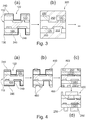
- Figure 3 and 4 show two process options for building up further built-up structured on both sides of a PCB, as obtained with the procedure illustrated in Figure 2 .
- Option I is illustrated in Figure 3
- Option II is illustrated in Figure 4 .
- a corresponding core-less process flow consists in manufacturing two PCBs constituted only of build-up layers (i.e. without a mechanically stabilizing core) on the two sides of a temporary carrier. After manufacturing, the two PCBs are separated from the temporary carrier.
- Figure 3 illustrates a full panel plating as Option I following the process shown in Figure 2 .
- Figure 3(a) which shows the starting point for the full panel plating option, is identical to Figure 2(e) described above.
- the full panel plating is realized by depositing an electrically conductive material 250 both on the upper side and the lower side of the structure shown in Figure 3(a) .
- the deposition of the electrically conductive material 250 is realized with a galvanic copper deposition within the recesses 122 and on the panel surface.
- FIG 3(b) As can be seen from the result of such a full panel plating, which result it is shown in Figure 3(b) , within the regions of the recesses 122 there are formed metallized via connections 252.
- the structure resulting from this is a component carrier 300.
- the component carrier 300 can be further processed either by using conventional subtractive etching or by using a so called modified semi additive process.
- SAP semi additive process
- a seed layer is deposited over the entire "naked" surface of a dielectric layer structure.
- a copper foil is present at the surface of the dielectric layer structure.
- Figure 4 illustrates a via filling and pattern plating including a further lithographic step as Option II following the process shown in Figure 2 . Also for Option II the starting point, which is depicted in Figure 4(a) , is the same as the structure shown in Figure 2(e) .
- a photoresist (film) 460 is applied and structured on both surfaces. This is shown in Figure 4(b) .
- a via and pattern plating procedure is executed again on both sides.
- an electrically conductive material 250 including fully metallized via connections 252 is deposited (on both sides).
- the photoresist 460 is stripped off, and the conductive layer below it is etched away.
- the structure resulting from this "stripping off” and etching is a component carrier 400.
- Figure 5 illustrates a process for contacting an electronic component 516 being embedded within a laminated PCB layer stack 510.
- the process is almost completely the same as the process illustrated in Figure 2 , including the two further processing options I and II shown in Figures 3 and 4 , respectively.
- the laminated PCB layer stack 510 accommodates the embedded electronic component 516 whereas the PCB 110 does not have an embedded component.
- the component 516 may be embedded or integrated completely within the body of the PCB 510.
- the electronic component may be accommodated within the PCB such that one surface of the component forms a part of the surface of the PCB.
- the metal layer structure 114 can be either an embedded trace-like structure or a conventional PCB, where a conductive track is formed on or over a dielectric layer structure.
- Figure 5(b) shows a laminated layer stack 590 with a PID layer 120 and an electrically conductive layer 130 laminated both on an upper side and a lower side of the laminated PCB layer stack 510.
- the electrically conductive layer 130 is a copper layer.
- Figure 5(c) shows the laminated layer stack after (i) a first lithographic process performed at or performed with both the upper copper layer 130 and the lower copper layer 130, after (ii) a corresponding copper etching, and after (iii) a usual photo resist (not depicted) stripping.
- Figure 5(d) shows the laminated layer stack after a second lithographic process performed with both PID layers 120. Thereby, recesses 122 within the PID layers 120 are formed.
- Figure 5(e) shows the laminated layer stack after a deposition of a seed layer, e.g. copper, 240. Further process options are shown in Figures 3 and 4 .
- a seed layer e.g. copper, 240.
- FIG. 6 illustrates a process for obtaining a redistribution layer (RDL) arrangement on fan-out/wafer level packages.
- RDL redistribution layer
- the starting point for a corresponding process is given by a plurality of layers. These layers include, from the bottom up, a lower electrically conductive layer 130, a lower PID layer 120, a (middle) layer stack 610, an upper PID layer 120, and an upper electrically conductive layer 130.
- the layer stack 610 comprises two artificial wafer structures 618 and a carrier structure 616 formed in between the two artificial wafer structures 618.
- the artificial wafer 618 comprises at least two unhoused/bare semiconductor components or naked chips.
- Figure 6(b) shows the corresponding laminated layer stack 619 which is obtained by means of a lamination of the two PID layers 120 and the two electrically conductive layers 130.
- Figure 6(c) shows the laminated layer stack after (i) a first lithographic process performed at or performed with both the upper copper layer 130 and the lower copper layer 130, after (ii) a corresponding copper etching, and after (iii) a usual photo resist (not depicted) stripping.
- Figure 6(d) shows the laminated layer stack after a second lithographic process performed with both PID layers 120. Thereby, a plurality of recesses 122 within the PID layers 120 are formed.
- Figure 7(b) shows the laminated layer stack after (i) a first lithographic process performed at or performed with the electrically conductive layer 130, after (ii) a corresponding selective etching away of portions of the electrically conductive layer 130 such that openings 132 are produced, and after (iii) a usual photo resist (not depicted) stripping.
- Figure 7(c) shows the laminated layer stack after (i) a second lithographic process performed at or performed with the PID layer 720 and after (ii) a (complete) removal of the remaining material of the electrically conductive layer structure 130.
- a second curing step might be necessary, either thermal or with electromagnetic radiation, before stripping off the PID material.
- Figure 7(d) shows the laminated layer stack after a removal of the not photo-imaged regions of the negative-type PID layer 720.
- the corresponding PID structured laminate is denominated a component carrier 700.
- the process described with reference to Figure7 leaves the "bare" PID material (i.e. no copper foil on it) unaffected.
- the roughness of the electrically conductive layer structure 130 which has been used as a mask for photo-imaging, will leave its profile imprinted within the PID layer 720.
- Such a roughness might be then used as mechanical adhesion, in addition to the chemical one achieved with an electroless deposition of copper (not depicted).
- conventional structuring processes can be used to proceed with the component carrier manufacturing.
- Figure 8 illustrates a cavity formation within a PID layer by using a patterned electrically conductive layer structure as a mask.
- FIG. 8(d) it is further processed by forming a cavity protection 870 within the upper cavity 822 within the PID layer 120.
- the lower cavity 822 remains unprotected.
- the cavity protection can be realized for instance by means of a screen printing procedure, a coverage during a lithographic process or any other appropriate procedure known to the skilled person.
- Figure 8(e) shows the corresponding structure which in this document, although representing an intermediate product, is denominated a component carrier 800.
Landscapes
- Engineering & Computer Science (AREA)
- Microelectronics & Electronic Packaging (AREA)
- Physics & Mathematics (AREA)
- Manufacturing & Machinery (AREA)
- Architecture (AREA)
- Structural Engineering (AREA)
- General Physics & Mathematics (AREA)
- Spectroscopy & Molecular Physics (AREA)
- Production Of Multi-Layered Print Wiring Board (AREA)
- Preparing Plates And Mask In Photomechanical Process (AREA)
Abstract
Description
- The present invention relates to the technical field of component carriers which are used as support structures for building up electronic assemblies (i.e. electronic circuits comprising one or more electronic components).
- A component carrier such as a Printed Circuit Boards (PCB) is a support structure for at least one electronic component forming an electronic assembly respectively an electronic circuit. Conductor traces representing an interconnecting wiring are formed from a thin metal layer comprising in particular copper. The conductor traces are formed by means of an appropriate structuring or patterning of an electrically conductive layer which is provided on top or beneath an electrically insulating layer of a component carrier. An electronic component may be mounted on an upper or lower surface of a component carrier. In some applications, an electronic component is embedded at least partially within (the volume of) a component carrier.
- A so called multilayer component carrier is a laminated stack consisting of several electrically conductive layer structures and several electrically insulating or dielectric layers in an alternating sequence. For electrically connecting different electrically conductive layer structures there may be used metallized vias extending at least through one electrically insulating layer.
- Electrically insulating or dielectric layer structures may be made e.g. from a resin which can be mechanically supported by a glass fiber mesh. However, also photosensitive or photoimagable resin can be employed for forming a dielectric layer structure of a component carrier. A photoimagable resin can be spatially structured first by exposing the photoimagable resin to spatially structured electromagnetic radiation and second by selectively etching away material from the photoimagable resin. For spatially structuring electromagnetic radiation impinging onto a photoimagable resin, a special mask has to be used as described for instance in
US 2014/0124777 A1 . With such a combination of photo-imaging and chemical etching, vias can be formed also within photoimagable resin. - There may be a need for a component carrier comprising a structured photoimagable dielectric layer which can be manufactured in an easy and effective manner.
- This need may be met by the subject matter according to the independent claims. Advantageous embodiments of the present invention are described by the dependent claims.
- According to a first aspect of the invention there is provided a component carrier which comprises (a) a layer stack comprising at least one component carrier material; and (b) a photoimagable dielectric layer structure formed on top of the layer stack. The photoimagable dielectric layer structure has at least one recess extending vertically through the photoimagable dielectric layer structure. The at least one recess is or has been formed by partially removing the photoimagable dielectric layer structure in regions which are defined by a spatial pattern of an electrically conductive layer structure being (directly) formed on the photoimagable dielectric layer structure. The spatial pattern comprises openings formed within the electrically conductive layer structure.
- The described component carrier is based on the idea that a photoimagable dielectric (PID) layer structure can be structured respectively patterned by exploiting the spatial design of a structured respectively patterned electrically conductive layer structure as a mask for the material of the PID layer (structure). Thereby, the at least one opening within the electrically conductive layer structure makes accessible the PID layer for a photo-imaging treatment e.g. by means of ultraviolet (UV) radiation. Since photo-imaging treatment procedures are well known to the skilled person, no further details about the basic principles of photo-imaging are given in this document.
- The described electrically conductive layer structure may not only be used as a mask for photo-imaging but at the same time may serve as a base layer for (a built-up of) further or additional electrically conductive layer structure(s) and/or dielectric layer structure(s) which may form a part of the described component carrier. Such an additional built-up arrangement may comprise e.g. a so called redistribution layer (RDL) arrangement which may make narrowly spaced electric contacts of an integrated electronic component available in other locations which are spaced apart from each other more widely.
- The layer stack may comprise different layers being formed one over the other. The different layers may comprise different materials. However, at least one material of at least one layer of the layer stack comprises a component carrier material or printed circuit board material as elucidated below. The layer stack and, as a consequence also the entire component carrier, may comprise a stack of at least one electrically insulating layer and at least one electrically conductive layer. For example, the layer stack respectively the component carrier may be a laminate of the mentioned electrically insulating layer(s) and electrically conductive layer(s), in particular formed by applying mechanical pressure and/or thermal energy. The component carrier, optionally being provided with respectively comprising further layer (structures) may provide a plate-shaped mounting base capable of providing a large mounting surface for further components and being nevertheless very thin and compact. The terms "layer" and/or "layer structure" may particularly denote a continuous layer, a patterned layer or a plurality of non-consecutive islands within a common plane.
- In the context of this document the term "component carrier" may particularly denote any support structure which is capable of accommodating one or more (electronic) components thereon and/or therein for providing mechanical support and/or electrical connectivity. In other words, a component carrier may be configured as a mechanical and/or electric carrier for electronic components. In particular, a component carrier may be one of a printed circuit board, an (organic) interposer, and an integrated circuit (IC) substrate. A component carrier may also be a hybrid board combining different ones of the above mentioned types of component carriers.
- The term "photoimagable" may particularly mean that upon an exposure of electromagnetic waves having an appropriate wavelength, e.g. UV light, the internal chemical and/or physical structure changes which causes a lithography process like developing for a via or a pattern formation. For some photoimagable dielectric (PID) materials, an exposure of light has the effect that the respective exposed portions become "unstable" and can be removed at least partially with an appropriate etching treatment. Such a type of PID material is often called positive PID material. Other PID materials become stable when being irradiated with or exposed to appropriate electromagnetic waves. This means, that upon an etching treatment only the irradiated portions of the PID material will remain stable and all other portions will be removed at least partially. This other type of PID materials are often denominated negative PID materials.
- Using the spatial pattern of the electrically conductive layer structure as a mask for structuring the PID layer may provide the advantage that by contrast to known structuring procedures such as e.g. laser ablation or mechanical cutting, the efficiency of the recess formation process can be significantly increased. Specifically, a parallelization of an etching formation of recesses can be realized such that in particular when a large number of recesses have to be formed, a corresponding throughput may be significantly, e.g. by a factor of 2 to 13, larger as compared to a throughput which can be realized with known PID structuring procedures. This of cause also reduces the process costs.
- According to an embodiment the component carrier comprises the electrically conductive layer structure formed on the photoimagable dielectric layer structure.
- As has been mentioned above in this embodiment the electrically conductive layer structure (having been previously used as a mask) forms a part of the (final) component carrier. Further, this embodiment can be realized in particular when using a positive PID material for the photoimagable dielectric layer structure. In a complete wording this embodiment can be described as follows:
A component carrier comprising (a) a layer stack comprising at least one component carrier material; (b) a photoimagable dielectric layer structure formed on the layer stack; and (c) an electrically conductive layer structure formed on the photoimagable dielectric layer structure, the electrically conductive layer structure having at least one opening; wherein the photoimagable dielectric layer structure has at least one recess being located under and spatially aligned with the opening of the electrically conductive layer structure. - In this context, the term "aligned" may particularly mean that with respect to an x-direction and a y-direction there is no offset between the opening formed in the electrically conductive layer structure and the respective recess formed in the PID layer structure. Thereby, the x-direction and the y-direction define a plane being parallel to the spatial extension of the various layers of the described component carrier. In other words, both the x-direction and the y-direction are perpendicular to a z-direction along which a thickness of the layer structures of the component carrier is measured.
- According to a further embodiment the electrically conductive layer structure having the openings formed therein comprises at least one of the group consisting of copper, aluminum, nickel, silver, titanium and gold. This may provide the advantage that for realizing the mask being used for exposing the PID layer, a common material being widely accepted for PCB manufacturing can be relied upon. This may facilitate the control of manufacturing the described component carrier.
- According to a further embodiment the component carrier further comprises an electrically conductive material provided within the at least one recess and/or formed on the electrically conductive layer structure.
- Depending on the specific application the at least one recess formed within the PID layer structure may be filled completely or may be filled only partially with the electrically conductive material. Alternatively or in combination, the electrically conductive layer structure may be covered with a certain thickness of the electrically conductive material.
- The electrically conductive material may be the same material as the material being used for the electrically conductive layer structure. This means that outside from the at least one recess the material of the electrically conductive layer structure and the described electrically conductive material may add up to a common amount of (single piece) material. This same material may be in particular copper.
- It is pointed out that before forming the described electrically conductive material a so called seed layer can be formed. Such a seed layer may comprise only a few atomic layers of the material being used in particular for the described electrically conductive material. A seed layer may be formed e.g. by means of an electroless plating procedure.
- According to a further embodiment the electrically conductive material provided within the at least one recess forms a via connection extending through the photoimagable dielectric layer structure. Alternatively or in combination, the electrically conductive material provided within the at least one recess forms a pattern within a plane being perpendicular to the vertical extension of the recess.
- Due to of the described spatially selective imaging of the PID layer structure the at least one recess can be realized by means of an appropriate etching procedure. This means that a via formation can be accomplished without a drilling procedure such as e.g. a mechanical drilling and/or a laser drilling. A particular advantage of etching the photo imaged PID layer structure can be seen that a large number of vias can be formed simultaneously with an appropriate etching procedure. Thereby, it is not necessary that all vias have the same size because a corresponding etching substance acts in a spatial selective manner on the PID material, wherein the location of the material being removed from the PID layer structure depends on the spatial design of the mask. In other words, also differently sized vias can be formed within one common (etching) process step.
- Compared in particular with laser drilling the described use of a location or position dependent etching may yield vias having a better geometry. Specifically, the etched vias may have an at least approximately perfect cylindrical shape with side walls which are much steeper as compared to truncated cone sidewalls which are typically produced with laser drilling.
- According to a further embodiment the electrically conductive material provided within the at least one recess forms a pattern within a plane being perpendicular to the vertical extension of the recess. This means that this pattern extends within a so called xy-plane which is parallel to a main plane of the layers of the described component carrier. This may allow to add further electric circuitry to the component carrier.
- According to a further embodiment the recess forms a cavity within the photoimagable dielectric layer structure. The cavity may be used for accommodating further components or structures. The cavity may extend completely through the PID layer structure. Alternatively, the cavity may only have a depth which is smaller than the thickness of the PID layer structure. Further, a plurality of recesses respectively cavities may have the same lateral size and/or depth. Alternatively, different recesses respectively cavities may have different spatial dimensions.
- According to a further embodiment the component carrier further comprises at least one component being accommodated within the at least one recess. The size of the at least one recess may be adapted to the size of the component. Specifically, in case of a comparatively thick PID layer structure and/or a comparatively thin component the recess may extend only partially through the PID layer structure.
- For accommodating respectively for embedding the component the size of the corresponding recess may be selected such that there is a gap between the side surface of a corresponding inner sidewall of the recess. In some embodiments this gap is filled with resin. In other embodiments the size of the recess is the same or is only slightly larger than the size of the component such that the component, after having been inserted into the recess, is accommodated in a spatially defined manner.
- The above mentioned "drilling less" etching procedure for vias may be of particular advantage when the described accommodated component is located in close proximity to a via which is supposed to be formed. Specifically, with the described etching procedure vias can be formed in close proximity on or over the accommodated component without the risk of damaging the component and/or damaging a redistribution layer (RDL) arrangement formed (directly) on or over the accommodated component. This may be an essential advantage compared to a formation of vias by means of laser drilling.
- According to a further embodiment the accommodated component is selected from a group consisting of an electronic component, an electrically non-conductive and/or electrically conductive inlay (such as a metal inlay, preferably comprising copper or aluminum), a heat transfer unit (for example a heat pipe), an energy harvesting unit, an active electronic component, a passive electronic component, an electronic chip, a storage device (for instance a DRAM or another data memory), a filter, an integrated circuit, a signal processing component, a power management component, an optoelectronic interface element, a light emitting diode, a photocoupler, a voltage converter (for example a DC/DC converter or an AC/DC converter), a cryptographic component, a transmitter and/or receiver, an electromechanical transducer, an actuator, a microelectromechanical system (MEMS), a microprocessor, a capacitor, a resistor, an inductance, an accumulator, a switch, a camera, an antenna, a magnetic element, a further component carrier and a logic chip.
- However, also other component types may be embedded in the component carrier. For example, a magnetic element can be used as a component. Such a magnetic element may be a permanent magnetic element (such as a ferromagnetic element, an antiferromagnetic element or a ferrimagnetic element, for instance a ferrite core) or may be a paramagnetic element. However, the component may also be a substrate, an interposer or a further component carrier such that a so called board-in-board configuration is realized. The component may be surface mounted on the component carrier and/or may be embedded in an interior thereof. Moreover, also other components, in particular those which generate and emit electromagnetic radiation and/or are sensitive with regard to electromagnetic radiation propagating from an environment, may be used as component.
- According to a further embodiment the component carrier further comprises a further photoimagable dielectric layer structure formed at the bottom of the layer stack, wherein the further photoimagable dielectric layer structure has at least one further recess extending vertically through the further photoimagable dielectric layer structure. The at least one further recess is formed by partially removing the further photoimagable dielectric layer structure in further regions which are defined by a further spatial pattern of a further electrically conductive layer structure being (directly) formed at the bottom of the further photoimagable dielectric layer structure. The further spatial pattern comprises further openings formed within the further electrically conductive layer structure.
- Descriptively speaking, the described component carrier comprises a sandwich type arrangement wherein the layer stack is located in between the two PID layer structures, i.e. the PID layer structure and the further PID layer structure. Thereby, in a cross sectional view, this arrangement may be symmetric with respect to a middle plane of the layer stack. Such a symmetric design may provide the advantage that mechanical stress which may occur during manufacturing the described component carrier may be the same at both sides (i.e. above and below) of this middle plane. In some embodiments, at least fractions of such a stress may be compensated with a corresponding stress occurring at the other side the middle plane.
- According to a further embodiment the layer stack comprises at least a part of a wafer, in particular a singularized semiconductor piece of a wafer.
- The part of the wafer may be at least one semiconductor chip which has been generated from the wafer by means of an appropriate separation or singularization procedure. Further, the wafer may be a so called artificial wafer, wherein the semiconductor chips of the original monolithic wafer have been singularized and placed on a carrier such as a sticky carrier foil in order to allow a further processing of simultaneously a plurality of semiconductor chips. Also a casting compound can be used for forming respectively realizing such an artificial wafer.
- Bare or naked semiconductor chips (without a housing) can be further processed easily and in a reliable manner when being integrated within or when forming part of the described layer stack. Specifically, by using the described PID layer structure and/or the electrically conductive layer structure, which has previously been used as the mask, further built-up structures can be generated for each semiconductor chip. Such a built-up may be e.g. a RDL arrangement. Of course, a built-up may also be act as a housing for protecting the respective semiconductor chip.
- According to a further embodiment the layer stack comprises (a) at least a part of a further wafer and (b) a carrier structure formed in between (the part of) the wafer and (the part of) the further wafer.
- In this embodiment the layer stack forms again a sandwich like arrangement, wherein the described carrier structure it is located in between (the part of) the wafer and (the part of) the further wafer. A further processing of the component carrier comprising two wafers may allow for a high efficiency respectively high throughput semiconductor component processing which may end up with housed semiconductor chips. Thereby, a highly efficient and reliable semiconductor further processing can be realized when the component carrier comprises at least two PID layer structures on both sides of the layer stack.
- In particular when the "double wafer layer stack" is realized in a symmetric manner a further processing of semiconductor chip(s) of the wafer and the further semiconductor chip(s) of the further wafer can be carried out in a precise and reliable manner. Specifically, mechanical stresses, e.g. caused by materials having different coefficients of thermal expansion (CTE), which mechanical stresses occur both above and below the carrier structure, may at least partially compensate each other.
- According to a further embodiment the component carrier is configured as a laminate-type component carrier. This may provide the advantage that the component carrier can be manufactured in a simple and an easy manner.
- According to a further embodiment the component carrier material comprises at least one of the group consisting of resin (such as reinforced or non-reinforced resins, for instance epoxy resin or Bismaleimide-Triazine resin, cyanate ester, polyphenylene derivate, glass (in particular glass fibers, multi-layer glass, glass-like materials), prepreg material (such as FR-4 or FR-5), polyimide, polyamide, liquid crystal polymer (LCP), epoxy-based Build-Up Film, polytetrafluoroethylene (Teflon), a ceramic, and a metal oxide. Reinforcing materials such as webs, fibers or spheres, for example made of glass (multilayer glass) may be used as well. Although prepreg such as FR4 are usually preferred for rigid PCBs, other materials (in particular epoxy-based Build-Up Film for substrates) may be used as well. For high frequency applications, high-frequency materials such as polytetrafluoroethylene, liquid crystal polymer and/or cyanate ester resins, low temperature cofired ceramics (LTCC) or other low, very low or ultra low DK-materials may be implemented in the component carrier as electrically insulating layer structure.
- According to a further embodiment the component carrier is configured as one of the group consisting of a printed circuit board and a substrate.
- In the context, the term "printed circuit board" (PCB) may particularly denote a component carrier which is formed by laminating several electrically conductive layer structures with at least one electrically insulating layer structure, for instance by applying pressure and/or thermal energy. A PCB may be plate-shaped (i.e. planar), three-dimensionally curved (for instance when manufactured using 3D printing) or may have any other shape. As preferred materials for PCB technology, the electrically conductive layer structures are made of copper, whereas the electrically insulating layer structures may comprise resin and/or glass fibers, so-called prepreg such as FR4 material. The various electrically conductive layer structures may be connected to one another in a desired way by forming through-holes through the laminate, for instance by laser drilling, mechanical drilling or etching, and by filling them at least partially with electrically conductive material such as in particular copper, thereby forming vias as through-hole connections. Apart from one or more components which may be embedded, a PCB is usually configured for accommodating one or more components on one or both opposing surfaces of the plate-shaped printed circuit board. They may be connected to the respective main surface by soldering. A dielectric part of a PCB may be composed of resin with reinforcing fibers such as e.g. glass fibers.
- In the context of the present application, the term "substrate" may particularly denote a small component carrier having substantially the same size as a component (in particular an electronic component) to be mounted thereon. More specifically, a substrate can be understood as a carrier for electrical connections or electrical networks as well as component carrier comparable to a printed circuit board (PCB), however with a considerably higher density of laterally and/or vertically arranged connections. Lateral connections are for example conductive paths, whereas vertical connections may be for example metallized holes or vias. These lateral and/or vertical connections are arranged within the substrate and can be used to provide electrical and/or mechanical connections of housed components or unhoused components (such as bare dies), particularly of IC chips, with a PCB or an intermediate PCB. Thus, the term "substrate" also includes "IC substrates". A dielectric part of a substrate may be composed of resin with reinforcing spheres (such as glass spheres).
- According to a further embodiment the layer stack comprises an electrically conductive material which comprises at least one of the group consisting of copper, aluminum, nickel, silver, gold, palladium, and tungsten, any of the mentioned materials being optionally coated with supra-conductive material such as graphene. Although copper is usually preferred, other materials or coated versions thereof are possible as well, in particular coated with supra-conductive material such as graphene.
- According to a further aspect there is provided a method for manufacturing a component carrier. The provided manufacturing method comprises (a) providing a layer stack comprising at least one component carrier material; (b) forming a photoimagable dielectric layer structure on the layer stack; (c) forming a spatial pattern of an electrically conductive layer structure on the photoimagable dielectric layer structure, wherein the spatial pattern comprises openings formed within the electrically conductive layer structure; (d) exposing the photoimagable dielectric layer structure to electromagnetic radiation, wherein the spatial pattern of the electrically conductive layer structure represents a mask for selectively exposing predefined regions of the photoimagable dielectric layer structure; and (e) selectively removing material from the photoimagable dielectric layer structure depending on the spatial pattern.
- Also the described method is based on the idea that at least one recess within a photoimagable dielectric (PID) layer structure can be formed by using a mask which is realized by a spatial pattern of an electrically conductive layer structure. In some embodiments the described electrically conductive layer structure is a temporary structure which, after completing the recess formation, is removed from the component carrier. However, in preferred embodiments the electrically conductive layer structure is also used as a base layer for (a built-up of) further or additional electrically conductive layer structure(s) and/or dielectric layer structure(s) which may form a part of the described component carrier. The PID material could be a thermal curable or photo curable resin, or combination of both.
- According to a further embodiment the layer stack, the photoimagable dielectric layer structure, and the electrically conductive layer structure are assembled together by a lamination procedure.
- Using a lamination procedure for mechanically connecting the described layers respectively layer structures may provide the advantage that all layer structures being necessary for the component carrier to be manufactured can be put together with a simple and efficient procedure. Thereby, the lamination procedure may be realized in such a manner that a stable layer attachment is possible even without using adhesive layers. Specifically, a lamination procedure may allow for a stable attachment (i) of the PID layer structure directly at the layer stack and (ii) of the electrically conductive layer structure directly at the PID layer structure.
- With regard to the lamination procedure described here the same considerations apply as for the above described lamination of the layer stack. This means that the lamination procedure may include applying a pressure and/or thermal energy.
- According to a further embodiment the method further comprises forming an electrically conductive material within at least one recess formed within the photoimagable dielectric layer structure and/or on the electrically conductive layer structure.
- The electrically conductive material may be deposited at the desired locations by means of any deposition procedure which may be used for a deposition of metallic materials. Preferably, the electrically conductive material may be formed by a galvanic deposition and in particular by a galvanic deposition of copper.
- It has to be noted that embodiments of the invention have been described with reference to different subject matters. In particular, some embodiments have been described with reference to apparatus claims whereas other embodiments have been described with reference to method type claims. However, a person skilled in the art will gather from the above and the following description that, unless other notified, in addition to any combination of features belonging to one type of subject matter also any combination between features relating to different subject matters, in particular between features of the apparatus type claims and features of the method type claims is considered as to be disclosed with this document.
- The aspects defined above and further aspects of the present invention are apparent from the examples of embodiment to be described hereinafter and are explained with reference to the examples of embodiment. The invention will be described in more detail hereinafter with reference to examples of embodiment but to which the invention is not limited.
-
- Figure 1
- illustrates a recess/via formation within a photoimagable dielectric (PID) layer structure by using a patterned electrically conductive layer structure as a mask for spatially selectively irradiating the PID layer with electromagnetic radiation.
- Figure 2
- illustrates a process overview for forming recesses/vias within two PID layers provided at different sides of a PCB layer stack.
- Figure 3
- illustrates a full panel plating as an option I following the process shown in
Figure 2 . - Figure 4
- illustrates a via filling and pattern plating including a further lithographic step as an option II following the process shown in
Figure 2 . - Figure 5
- illustrates a process for contacting an electronic component being embedded within a PCB.
- Figure 6
- illustrates a process for obtaining a redistribution layer (RDL) arrangement on fan-out/wafer level packages or panel-level packages.
- Figure 7
- illustrates a recess/via formation within a negative type PID layer.
- Figure 8
- illustrates a cavity formation within a PID layer by using a patterned electrically conductive layer structure as a mask.
- The illustration in the drawing is schematic. It is noted that in different figures, similar or identical elements or features are provided with the same reference signs or with reference signs, which are different from the corresponding reference signs only within the first digit. In order to avoid unnecessary repetitions elements or features, which have already been elucidated with respect to a previously described embodiment, are not elucidated again at a later position of the description.
- Further, spatially relative terms, such as "front" and "back", "above" and "below", "left" and "right", et cetera are used to describe an element's relationship to another element(s) as illustrated in the Figures. Thus, the spatially relative terms may apply to orientations in use which differ from the orientation depicted in the Figures. Obviously all such spatially relative terms refer to the orientation shown in the Figures only for ease of description and are not necessarily limiting as an apparatus according to an embodiment of the invention can assume orientations different than those illustrated in the Figures when in use.
-
Figure 1 illustrates the main steps of a recess respectively a via formation within a photoimagable dielectric (PID) layer structure of a component carrier in accordance with an embodiment of the invention.Figure 1(a) shows alaminated layer stack 190 which represents the starting point for manufacturing the component carrier. Thelaminated stack 190 comprises a usual laminatedPCB layer stack 110, which itself comprises at least one layer sequence consisting of a dielectric resin layer and metal layer structure. InFigure 1(a) thePCB layer stack 110 is depicted as a single layer PCB having only onedielectric resin layer 112 and one structuredmetal layer 114. However, in many embodiments the laminatedPCB layer stack 110 comprises two, three, or even more of such layer sequences. - On top of the laminated
PCB layer stack 110 there is formed photosensitive respectively a photoimagable dielectric (PID)layer 120. The PID layer may have a thickness of e.g. 10 µm to 100 µm. On top of thePID layer 120 there is formed a so far unstructured electricallyconductive layer 130. The electricallyconductive layer 130, which according to the embodiment described here is made from copper, may have a thickness of e.g. 0.1 µm to 50 µm. - It is pointed out that in the embodiment described here the
layer stack 110 could be a conventional PCB with conductive tracks formed on a dielectric layer. However, alternatively a so called embedded conductive track stack up could be used, in which the conductive track is at the same height or slightly below the dielectric surface. This alternative could be chosen also for all other embodiments described here with reference to the other Figured which are elucidated below. - By means of a first lithographic process a window is formed within the electrically
conductive layer 130. This can be seen inFigure 1(b) , the window, which in this document is called an opening, is denominated withreference numeral 132. - In a next step the upper side of the structure shown in
Figure 1(b) is irradiated with electromagnetic radiation. Thereby, the now structured electrically conductive layer 113 acts as a mask for selectively exposing thePID layer 120 within the region being aligned with theopening 132. By means of this treatment the respective material of thePID layer 120 gets sensitive to a chemical etching process. - The result of a corresponding etching process is shown in
Figure 1(c) . The respective material of thePID layer 120 has been removed such that arecess 122 is formed within the now structuredPID layer 120. The two steps of photo imaging thePID layer 120 through theopening 132 and the following (chemical) etching of thePID layer 120 selectively within the region of theopening 132 can be seen as a second lithographic process. - Although the arrangement shown in
Figure 1(c) may be an intermediate product for further manufacturing electronic devices, in this document this arrangement is denominated acomponent carrier 100. For instance, the structured electricallyconductive layer 130, which has been used as a mask, can be used for building up non-depicted further electrically insulating and/or electrically conductive structures of a larger electronic device. An example for such a built-up is a so called fan-out redistribution layer (RDL) arrangement. - Descriptively speaking, the process for manufacturing the
component carrier 100 can be seen as a two-stage lithographic process wherein first within the electricallyconductive layer 130 the windows being necessary for forming the recesses such as vias or cavities are realized. In a second lithographic process thePID layer 120 is structured such that therecesses 122 are formed. In the second lithography process the electricallyconductive layer structure 130 serves as a mask for thePID layer 120 below. Hence, no (dedicated) masks are needed for appropriately structuring thePID layer 120. The roughness of the electricallyconductive layer structure 130 itself will provide the necessary adhesion of the electricallyconductive layer structure 130 to thePID layer 120 formed below. In addition, also chemical adhesion layers could be provided in between the conductive layer structure and the PID, in particular for applications requiring high reliability in terms of peeling strength performance. - The benefit of the described PID structuring is the possibility to obtain "z-direction structures", i.e. structures extending into a direction being perpendicular to the main planes of the layers, with different geometries by means of one exposure step. Therefore, vias with different diameters can be effectively achieved on one and the same the
same PID layer 120. Further, also trenches or cavities with appropriate spatial dimensions can be realized. -
Figure 2 illustrates a process overview for forming recesses respectively vias within two PID layers provided at different sides of a PCB layer stack. -
Figure 2(a) shows various so far separate layers before a lamination. Specifically, the so far separate layers include, from the bottom up, a lower electricallyconductive layer 130, alower PID layer 120, a (middle) laminatedPCB layer stack 110, anupper PID layer 120, and an upper electricallyconductive layer 130. In the embodiment described here thePCB layer stack 110 is embedded in a trace-like manner. However, it could also be realized with a conventional stack-up such as that shown inFigure 1 . Further, in the embodiment described here the laminatedPCB layer stack 110 comprises twometal layer structures 114 and adielectric resin layer 112 formed in between the twometal layer structures 114. It is pointed out that thePCB layer stack 110 could also comprise more than two layers, which could be denominated a multi-layer stack-up. -
Figure 2(b) shows the arrangement ofFigure 2(a) after lamination. In this document the corresponding laminated arrangement is denominated alaminated layer stack 290.Figure 2(c) shows the laminated arrangement after the upper electricallyconductive layer 130 and the lower electricallyconductive layer 130 have been structured such thatopenings 132 are formed (by means of a first lithographic process).Figure 2(d) shows the result of the second lithographic process, wherein in the region being aligned with theopenings 132 material of the PID layers 120 has been selectively removed such thatcorresponding recesses 122 are formed. In the embodiment described here, therecesses 122 expose or uncover portions of the twometal layer structures 114. - In a next step, the result of which is shown in
Figure 2(e) , aseed layer 240 is deposited both on the upper side and the lower side of the structure shown inFigure 2(d) . According to the embodiment described here theseed layer 240 is formed by means of an electroless deposition of copper, or dry process deposition such as sputtering. - Descriptively speaking,
Figure 3 and 4 show two process options for building up further built-up structured on both sides of a PCB, as obtained with the procedure illustrated inFigure 2 . Option I is illustrated inFigure 3 , Option II is illustrated inFigure 4 . - It is pointed out that the process described above can be applied also for core-less layer stacks being sandwiches between two PID layers. A corresponding core-less process flow consists in manufacturing two PCBs constituted only of build-up layers (i.e. without a mechanically stabilizing core) on the two sides of a temporary carrier. After manufacturing, the two PCBs are separated from the temporary carrier.
-
Figure 3 illustrates a full panel plating as Option I following the process shown inFigure 2 .Figure 3(a) , which shows the starting point for the full panel plating option, is identical toFigure 2(e) described above. According to the embodiment described here, the full panel plating is realized by depositing an electricallyconductive material 250 both on the upper side and the lower side of the structure shown inFigure 3(a) . Specifically, according to the embodiment described here, the deposition of the electricallyconductive material 250 is realized with a galvanic copper deposition within therecesses 122 and on the panel surface. As can be seen from the result of such a full panel plating, which result it is shown inFigure 3(b) , within the regions of therecesses 122 there are formed metallized viaconnections 252. In this document the structure resulting from this is acomponent carrier 300. Thecomponent carrier 300 can be further processed either by using conventional subtractive etching or by using a so called modified semi additive process. In this regard it is mentioned that in a conventional semi additive process (SAP) a seed layer is deposited over the entire "naked" surface of a dielectric layer structure. In a modified SAP, a copper foil is present at the surface of the dielectric layer structure. -
Figure 4 illustrates a via filling and pattern plating including a further lithographic step as Option II following the process shown inFigure 2 . Also for Option II the starting point, which is depicted inFigure 4(a) , is the same as the structure shown inFigure 2(e) . - In the beginning of Option II, by means of a further lithographic process, a photoresist (film) 460 is applied and structured on both surfaces. This is shown in
Figure 4(b) . Afterwards, a via and pattern plating procedure is executed again on both sides. Thereby, as can be seen fromFigure 4(c) , an electricallyconductive material 250 including fully metallized viaconnections 252 is deposited (on both sides). Finally, as can be seen fromFigure 4(d) , thephotoresist 460 is stripped off, and the conductive layer below it is etched away. In this document the structure resulting from this "stripping off" and etching is acomponent carrier 400. -
Figure 5 illustrates a process for contacting anelectronic component 516 being embedded within a laminatedPCB layer stack 510. The process is almost completely the same as the process illustrated inFigure 2 , including the two further processing options I and II shown inFigures 3 and 4 , respectively. As can be taken already fromFigure 5(a) the only difference between these two processes is that the laminatedPCB layer stack 510 accommodates the embeddedelectronic component 516 whereas thePCB 110 does not have an embedded component. In accordance with the embodiment described here thecomponent 516 may be embedded or integrated completely within the body of thePCB 510. Alternatively, the electronic component may be accommodated within the PCB such that one surface of the component forms a part of the surface of the PCB. At this point it is mentioned again that themetal layer structure 114 can be either an embedded trace-like structure or a conventional PCB, where a conductive track is formed on or over a dielectric layer structure. -
Figure 5(b) shows alaminated layer stack 590 with aPID layer 120 and an electricallyconductive layer 130 laminated both on an upper side and a lower side of the laminatedPCB layer stack 510. Again, also in the embodiment described here the electricallyconductive layer 130 is a copper layer. -
Figure 5(c) shows the laminated layer stack after (i) a first lithographic process performed at or performed with both theupper copper layer 130 and thelower copper layer 130, after (ii) a corresponding copper etching, and after (iii) a usual photo resist (not depicted) stripping. -
Figure 5(d) shows the laminated layer stack after a second lithographic process performed with both PID layers 120. Thereby, recesses 122 within the PID layers 120 are formed. -
Figure 5(e) shows the laminated layer stack after a deposition of a seed layer, e.g. copper, 240. Further process options are shown inFigures 3 and 4 . - The above elucidated principles of structuring a PID layer with a lithographic process, wherein a mask representing a structured electrically conductive layer of the final product is employed, can also be applied to wafer/panel level packaging (WLP/PLP) manufacturing methods. In this context
Figure 6 illustrates a process for obtaining a redistribution layer (RDL) arrangement on fan-out/wafer level packages. - The starting point for a corresponding process, which starting point is illustrated in
Figure 6(a) , is given by a plurality of layers. These layers include, from the bottom up, a lower electricallyconductive layer 130, alower PID layer 120, a (middle)layer stack 610, anupper PID layer 120, and an upper electricallyconductive layer 130. In the embodiment described here thelayer stack 610 comprises twoartificial wafer structures 618 and acarrier structure 616 formed in between the twoartificial wafer structures 618. Theartificial wafer 618 comprises at least two unhoused/bare semiconductor components or naked chips. -
Figure 6(b) , shows the corresponding laminated layer stack 619 which is obtained by means of a lamination of the twoPID layers 120 and the two electricallyconductive layers 130. -
Figure 6(c) shows the laminated layer stack after (i) a first lithographic process performed at or performed with both theupper copper layer 130 and thelower copper layer 130, after (ii) a corresponding copper etching, and after (iii) a usual photo resist (not depicted) stripping. -
Figure 6(d) shows the laminated layer stack after a second lithographic process performed with both PID layers 120. Thereby, a plurality ofrecesses 122 within the PID layers 120 are formed. - Further processing steps, which for the sake of conciseness of
Figure 6 are only mentioned (and not depicted) are (i) a copper seed layer deposition, (ii) a further processing either with one of the above elucidated options I and II, (iii) further process repetitions for obtaining further RDL structures or RDL arrangements, and (iv) a component separation in order to obtain a plurality of singularized and (fan-out) packaged semiconductor components. - So far, the processes described are referring to a so called positive-type PID, i.e. the PID is structured where the exposure occurs. However, corresponding processes can also be realized for negative-type PID. This means that PID material will be removed on the non-exposed parts. A corresponding process overview for a negative-type PID is shown in
Figure 7 . Thereby, apart from employing a negativetype PID layer 720 the starting point shown inFigure 7(a) is very similar to the laminate structure shown inFigure 1(a) . -
Figure 7(b) shows the laminated layer stack after (i) a first lithographic process performed at or performed with the electricallyconductive layer 130, after (ii) a corresponding selective etching away of portions of the electricallyconductive layer 130 such thatopenings 132 are produced, and after (iii) a usual photo resist (not depicted) stripping. -
Figure 7(c) shows the laminated layer stack after (i) a second lithographic process performed at or performed with thePID layer 720 and after (ii) a (complete) removal of the remaining material of the electricallyconductive layer structure 130. A second curing step might be necessary, either thermal or with electromagnetic radiation, before stripping off the PID material. -
Figure 7(d) shows the laminated layer stack after a removal of the not photo-imaged regions of the negative-type PID layer 720. In this document the corresponding PID structured laminate is denominated acomponent carrier 700. - Descriptively speaking, the process described with reference to
Figure7 leaves the "bare" PID material (i.e. no copper foil on it) unaffected. However, the roughness of the electricallyconductive layer structure 130, which has been used as a mask for photo-imaging, will leave its profile imprinted within thePID layer 720. Such a roughness might be then used as mechanical adhesion, in addition to the chemical one achieved with an electroless deposition of copper (not depicted). Afterwards, conventional structuring processes can be used to proceed with the component carrier manufacturing. - The structuring methods elucidated above can also be used to obtain any kind of z-direction structures, like vias, cavities, trenches, etc.
Figure 8 illustrates a cavity formation within a PID layer by using a patterned electrically conductive layer structure as a mask. - The corresponding process steps or intermediate products, which are depicted in
Figure 8(a), Figure 8(b), and Figure 8(c) , fully correspond to the process steps or intermediate products shown in above elucidatedFigure 2(a), Figure 2(b), and Figure 2(c) , respectively. The only difference betweenFigure 8(c) andFigure 2(c) is that anopening 832 within the electricallyconductive layer structure 130 is much larger that theopening 132. Correspondingly, also therecess 822 representing acavity 822 shown inFigure 8(d) is much larger than therecess 122 shown inFigure 2(d) . - The arrangement shown in
Figure 8(d) it is further processed by forming acavity protection 870 within theupper cavity 822 within thePID layer 120. According to the embodiment described here thelower cavity 822 remains unprotected. The cavity protection can be realized for instance by means of a screen printing procedure, a coverage during a lithographic process or any other appropriate procedure known to the skilled person.Figure 8(e) shows the corresponding structure which in this document, although representing an intermediate product, is denominated acomponent carrier 800. - As can be taken from
Figure 8 , a further processing can be carried out again with the two process options I and II as shown in above elucidatedFigure 3 and Figure 4 , respectively. - The invention or the embodiments of the invention described in this document can be descriptively and briefly summarized as follows: With this document a structuring method of PID is presented, which is based on exploiting a structured copper foil as a mask for the PID layer itself. Subsequently, electroless copper will be deposited in particular on the sidewalls of recesses (e.g. vias) formed within the PID material. Further subsequently, a copper plating executed. A similar strategy can be adopted in order to form recess portions within a PCB.
- It should be noted that the term "comprising" does not exclude other elements or steps and the use of articles "a" or "an" does not exclude a plurality. Also elements described in association with different embodiments may be combined. It should also be noted that reference signs in the claims should not be construed as limiting the scope of the claims.
-
- 100
- component carrier
- 110
- layer stack / laminated PCB layer stack / PCB core
- 112
- dielectric resin layer
- 114
- metal layer structure
- 120
- photoimagable dielectric layer (structure)
- 122
- recess
- 130
- electrically conductive layer structure / mask
- 132
- opening
- 190
- laminated layer stack
- 240
- seed layer
- 250
- electrically conductive material
- 252
- via connection
- 290
- laminated layer stack
- 300
- component carrier
- 400
- component carrier
- 460
- photoresist
- 510
- layer stack / laminated PCB layer stack
- 516
- embedded component
- 590
- laminated layer stack
- 610
- layer stack
- 616
- carrier structure
- 618
- naked chip / bare semiconductor component / artificial wafer
- 690
- laminated layer stack
- 700
- component carrier
- 720
- negative type photoimagable dielectric layer (structure)
- 800
- component carrier
- 822
- cavity
- 832
- opening for cavity
- 870
- cavity protection
Claims (15)
- A component carrier (100) comprisinga layer stack (110) comprising at least one component carrier material; anda photoimagable dielectric layer structure (120) formed on top of the layer stack (110),wherein the photoimagable dielectric layer structure (120) has at least one recess (122) extending vertically through the photoimagable dielectric layer structure (120),
the at least one recess (122) being formed by partially removing the photoimagable dielectric layer structure (120) in regions which are defined by a spatial pattern of an electrically conductive layer structure (130) being formed on the photoimagable dielectric layer structure (120), wherein the spatial pattern comprises openings (132) formed within the electrically conductive layer structure (130). - The component carrier (100) as set forth in the preceding claim, further comprising
the electrically conductive layer structure (130) formed on the photoimagable dielectric layer structure (120). - The component carrier (100) as set forth in any one of the preceding claims, wherein
the electrically conductive layer structure (130) having the openings (132) formed therein comprises at least one of the group consisting of copper, aluminum, nickel, silver, titanium, and gold. - The component carrier (300) as set forth in any one of the preceding claims, further comprising
an electrically conductive material (250) provided within the at least one recess (122) and/or formed on the electrically conductive layer structure (130). - The component carrier (300) as set forth in the preceding claim, wherein
the electrically conductive material (250) provided within the at least one recess (122) forms at least one of
a via connection (252) extending through the photoimagable dielectric layer structure (120) and
a pattern within a plane being perpendicular to the vertical extension of the recess (122). - The component carrier (100, 300) as set forth in any one of the preceding claims, wherein
the recess (122) forms a cavity within the photoimagable dielectric layer structure (120). - The component carrier (100, 300) as set forth in the preceding claim, further comprising
at least one component being accommodated within the at least one recess (122). - The component carrier (100, 300) as set forth in the preceding claim, wherein the accommodated component is selected from a group consisting of an electronic component, an electrically non-conductive and/or electrically conductive inlay, a heat transfer unit, an energy harvesting unit, an active electronic component, a passive electronic component, an electronic chip, a storage device, a filter, an integrated circuit, a signal processing component, a power management component, an optoelectronic interface element, a voltage converter, a cryptographic component, a transmitter and/or receiver, an electromechanical transducer, an actuator, a microelectromechanical system, a microprocessor, a capacitor, a resistor, an inductance, an accumulator, a switch, a camera, an antenna, a magnetic element, a further component carrier and a logic chip.
- The component carrier (300, 400) as set forth in any one of the preceding claims, further comprising
a further photoimagable dielectric layer structure (120) formed at the bottom of the layer stack (110), wherein the further photoimagable dielectric layer structure (120) has at least one further recess (122) extending vertically through the further photoimagable dielectric layer structure (120),
the at least one further recess (122) being formed by partially removing the further photoimagable dielectric layer structure (120) in further regions which are defined by a further spatial pattern of a further electrically conductive layer structure (250) being formed at the bottom of the further photoimagable dielectric layer structure (120), wherein the further spatial pattern comprises further openings (132) formed within the further electrically conductive layer structure (250). - The component carrier as set forth in any one of the preceding claims, wherein
the layer stack comprises at least a part of a wafer (618), in particular a singularized semiconductor piece (618) of a wafer. - The component carrier as set forth in the preceding claim, wherein the layer stack comprisesat least a part of a further wafer (618) anda carrier structure (616) formed in between the wafer (618) and the further wafer (618).
- The component carrier (100) as set forth in any one of the preceding claims, wherein the component carrier (100) comprises at least one of the following featu res:(a) the component carrier (100) is configured as a laminate-type component carrier;(b) the component carrier material comprises at least one of the group consisting of resin, in particular reinforced or non-reinforced resin, for instance epoxy resin or Bismaleimide-Triazine resin, cyanate ester, polyphenylene derivate, glass, prepreg material, polyimide, polyamide, liquid crystal polymer, epoxy-based Build-Up Film, polytetrafluoroethylene, a ceramic, and a metal oxide;(c) the component carrier (100) is configured as one of the group consisting of a printed circuit board and a substrate;(d) the layer stack (110) comprises an electrically conductive material which comprises at least one of the group consisting of copper, aluminum, nickel, silver, gold, palladium, and tungsten, any of the mentioned materials being optionally coated with supra-conductive material such as graphene.
- A method for manufacturing a component carrier (100), the method comprisingproviding a layer stack (110) comprising at least one component carrier material;forming a photoimagable dielectric layer structure (120) on the layer stack (110);forming a spatial pattern of an electrically conductive layer structure (130) on the photoimagable dielectric layer structure (120), wherein the spatial pattern comprises openings (132) formed within the electrically conductive layer structure (130);exposing the photoimagable dielectric layer structure (120) to electromagnetic radiation, wherein the spatial pattern of the electrically conductive layer structure (130) represents a mask for selectively exposing predefined regions of the photoimagable dielectric layer structure (120); andselectively removing material from the photoimagable dielectric layer structure (120) depending on the spatial pattern.
- The method as set forth in the preceding claim, wherein
the layer stack (110), the photoimagable dielectric layer structure (120), and the electrically conductive layer structure (130) are assembled together by a lamination procedure. - The method as set forth in the preceding claim, further comprising
forming an electrically conductive material (250) within at least one recess (122) formed within the photoimagable dielectric layer structure (120) and/or on the electrically conductive layer structure (130).
Applications Claiming Priority (1)
| Application Number | Priority Date | Filing Date | Title |
|---|---|---|---|
| US16/126,878 US20200083154A1 (en) | 2018-09-10 | 2018-09-10 | Component Carrier With a Photoimageable Dielectric Layer and a Structured Conductive Layer Being Used as a Mask for Selectively Exposing the Photoimageable Dielectric Layer With Electromagnetic Radiation |
Publications (3)
| Publication Number | Publication Date |
|---|---|
| EP3621103A2 true EP3621103A2 (en) | 2020-03-11 |
| EP3621103A3 EP3621103A3 (en) | 2020-03-18 |
| EP3621103B1 EP3621103B1 (en) | 2021-10-27 |
Family
ID=67809227
Family Applications (1)
| Application Number | Title | Priority Date | Filing Date |
|---|---|---|---|
| EP19193661.6A Active EP3621103B1 (en) | 2018-09-10 | 2019-08-27 | Component carrier with a photoimagable dielectric layer and a structured conductive layer being used as a mask for selectively exposing the photoimagable dielectric layer with electromagnetic radiation |
Country Status (3)
| Country | Link |
|---|---|
| US (3) | US20200083154A1 (en) |
| EP (1) | EP3621103B1 (en) |
| CN (1) | CN110891366B (en) |
Families Citing this family (2)
| Publication number | Priority date | Publication date | Assignee | Title |
|---|---|---|---|---|
| CN111508926B (en) | 2019-01-31 | 2022-08-30 | 奥特斯(中国)有限公司 | Component carrier and method for producing a component carrier |
| US20220406618A1 (en) * | 2021-06-18 | 2022-12-22 | Intel Corporation | Technologies for aligned vias over multiple layers |
Citations (1)
| Publication number | Priority date | Publication date | Assignee | Title |
|---|---|---|---|---|
| US20140124777A1 (en) | 2012-03-27 | 2014-05-08 | Panasonic Corporation | Built-up substrate, method for manufacturing same, and semiconductor integrated circuit package |
Family Cites Families (54)
| Publication number | Priority date | Publication date | Assignee | Title |
|---|---|---|---|---|
| JPH0350887A (en) | 1989-07-19 | 1991-03-05 | Hitachi Aic Inc | Manufacture of printed wiring board |
| US5689428A (en) | 1990-09-28 | 1997-11-18 | Texas Instruments Incorporated | Integrated circuits, transistors, data processing systems, printed wiring boards, digital computers, smart power devices, and processes of manufacture |
| JPH06275950A (en) | 1993-03-22 | 1994-09-30 | Hitachi Chem Co Ltd | Manufacture of wiring board |
| JPH0818239A (en) | 1994-07-04 | 1996-01-19 | Hitachi Ltd | Manufacturing method of multilayer printed wiring board |
| JPH1098266A (en) | 1996-09-20 | 1998-04-14 | Hitachi Chem Co Ltd | Photosensitive insulation material and manufacture of wiring board using the same |
| JPH10209644A (en) * | 1997-01-16 | 1998-08-07 | Nippon Steel Chem Co Ltd | Method for manufacturing multilayer wiring board |
| US5885745A (en) | 1997-04-28 | 1999-03-23 | Hitachi Chemical Co., Ltd. | Photoimageable compositions comprising polyquinoline polymer and photogenerable acid precursor |
| US6027858A (en) * | 1997-06-06 | 2000-02-22 | International Business Machines Corporation | Process for tenting PTH's with PID dry film |
| JPH11212272A (en) | 1998-01-29 | 1999-08-06 | Hitachi Chem Co Ltd | Relief pattern, relief pattern for additive, relief pattern for forming barrier, production of relief pattern and photosensitive element used in same |
| JP2000133935A (en) | 1998-10-28 | 2000-05-12 | Hitachi Chem Co Ltd | Manufacturing method of multilayer printed wiring board and multilayer printed wiring board manufactured by the method |
| US6349456B1 (en) * | 1998-12-31 | 2002-02-26 | Motorola, Inc. | Method of manufacturing photodefined integral capacitor with self-aligned dielectric and electrodes |
| TW512467B (en) * | 1999-10-12 | 2002-12-01 | North Kk | Wiring circuit substrate and manufacturing method therefor |
| US6521844B1 (en) * | 1999-10-29 | 2003-02-18 | International Business Machines Corporation | Through hole in a photoimageable dielectric structure with wired and uncured dielectric |
| US6960822B2 (en) * | 2002-08-15 | 2005-11-01 | Advanced Semiconductor Engineering, Inc. | Solder mask and structure of a substrate |
| KR100455892B1 (en) | 2002-12-30 | 2004-11-06 | 삼성전기주식회사 | Build-up printed circuit board and manufacturing method thereof |
| JP2004341478A (en) | 2003-04-25 | 2004-12-02 | Hitachi Chem Co Ltd | Photosensitive element, resist pattern forming method using the same, method for manufacturing printed circuit board and photosensitive resin composition |
| JP2005037755A (en) | 2003-07-17 | 2005-02-10 | Toyo Ink Mfg Co Ltd | Photosensitive resin composition, photosensitive film using same, and its manufacturing method |
| JP2005037754A (en) | 2003-07-17 | 2005-02-10 | Toyo Ink Mfg Co Ltd | Photosensitive resin composition, photosensitive film using the same, and method for producing the same |
| WO2006011548A1 (en) | 2004-07-30 | 2006-02-02 | Hitachi Chemical Company, Ltd. | Photosensitive film, photosensitive film laminate and photosensitive film roll |
| US8987808B2 (en) * | 2006-03-29 | 2015-03-24 | Cambridge Enterprise Limited | Thin film transistor with accurately aligned electrode patterns and electronic device(s) that include same |
| KR100743651B1 (en) * | 2006-05-24 | 2007-07-27 | 주식회사 하이닉스반도체 | Contact formation method of semiconductor device |
| WO2012081680A1 (en) | 2010-12-16 | 2012-06-21 | 日立化成工業株式会社 | Photosensitive element, method for forming resist pattern, and method for producing printed circuit board |
| TWM408911U (en) * | 2011-01-13 | 2011-08-01 | Mao Bang Electronic Co Ltd | Multilayer circuit board structure |
| KR101846589B1 (en) * | 2011-10-28 | 2018-04-06 | 가부시키가이샤 제이올레드 | Thin film semiconductor device and method for manufacturing thin film semiconductor device |
| TWI499023B (en) | 2012-10-11 | 2015-09-01 | 財團法人工業技術研究院 | Package substrate and its preparation method |
| CN103094287B (en) * | 2013-01-31 | 2015-12-09 | 北京京东方光电科技有限公司 | Array base palte and preparation method thereof, display unit |
| JP6273690B2 (en) | 2013-04-08 | 2018-02-07 | 日立化成株式会社 | Photosensitive resin composition and photosensitive film using the same |
| CN105164585B (en) | 2013-04-18 | 2020-02-21 | 太阳油墨制造株式会社 | Laminated structure, flexible printed circuit board, and manufacturing method thereof |
| JP6013975B2 (en) | 2013-06-05 | 2016-10-25 | 三菱製紙株式会社 | Pattern formation method |
| JP6318484B2 (en) | 2013-07-09 | 2018-05-09 | 日立化成株式会社 | Photosensitive resin composition, photosensitive element, resist pattern forming method and printed wiring board manufacturing method |
| TW201513753A (en) | 2013-09-26 | 2015-04-01 | Unimicron Technology Corp | Manufacturing method of circuit board |
| CN105683836B (en) | 2013-10-30 | 2019-11-08 | 太阳油墨制造株式会社 | Photosensitive thermosetting resin composition and flexible printed circuit board |
| KR102375653B1 (en) | 2014-02-12 | 2022-03-16 | 쇼와덴코머티리얼즈가부시끼가이샤 | Photosensitive element |
| US9406531B1 (en) * | 2014-03-28 | 2016-08-02 | STATS ChipPAC Pte. Ltd. | Integrated circuit packaging system with photoimagable dielectric-defined trace and method of manufacture thereof |
| US9679841B2 (en) | 2014-05-13 | 2017-06-13 | Qualcomm Incorporated | Substrate and method of forming the same |
| KR102582577B1 (en) | 2014-05-23 | 2023-09-25 | 가부시끼가이샤 레조낙 | Method for forming resist pattern, method for manufacturing printed wiring board, photosensitive resin composition for projection exposure and photosensitive element |
| JP5882510B2 (en) | 2014-06-30 | 2016-03-09 | 太陽インキ製造株式会社 | Photosensitive dry film and method for producing printed wiring board using the same |
| JP2016034010A (en) | 2014-07-29 | 2016-03-10 | 日立化成株式会社 | Method for forming metal pattern, and pattern substrate |
| CN106796402B (en) | 2014-10-16 | 2020-09-08 | 太阳油墨制造株式会社 | Laminated structures, dry films, and flexible printed circuit boards |
| KR102501454B1 (en) | 2014-10-17 | 2023-02-20 | 다이요 잉키 세이조 가부시키가이샤 | Dry film and flexible printed wiring board |
| WO2016158362A1 (en) | 2015-03-27 | 2016-10-06 | 日立化成株式会社 | Dry film, cured product, laminate, and method for forming resist pattern |
| JP6569268B2 (en) | 2015-03-30 | 2019-09-04 | 日立化成株式会社 | Photosensitive resin composition, photosensitive element, resist pattern forming method, and semiconductor component manufacturing method |
| JP2016213299A (en) | 2015-05-07 | 2016-12-15 | 日立化成株式会社 | Method for forming metal pattern and substrate with metal pattern |
| JP6596957B2 (en) | 2015-06-15 | 2019-10-30 | 日立化成株式会社 | Structure having conductor circuit, method for producing the same, and photosensitive resin composition |
| MY189073A (en) | 2015-07-08 | 2022-01-24 | Hitachi Chemical Co Ltd | Photosensitive element, laminated body, method for forming resist pattern, and method for producing printed circuit board |
| US20170018501A1 (en) | 2015-07-14 | 2017-01-19 | Avago Technologies General Ip (Singapore) Pte. Ltd | Via structures for thermal dissipation |
| US9401350B1 (en) | 2015-07-29 | 2016-07-26 | Qualcomm Incorporated | Package-on-package (POP) structure including multiple dies |
| KR102572426B1 (en) | 2015-07-30 | 2023-08-30 | 가부시끼가이샤 레조낙 | Photosensitive element, resin composition for forming barrier layer, method for forming resist pattern, and method for producing printed wiring board |
| US9775246B2 (en) * | 2015-08-07 | 2017-09-26 | Unimicron Technology Corp. | Circuit board and manufacturing method thereof |
| KR20170033191A (en) | 2015-09-16 | 2017-03-24 | 삼성전기주식회사 | Printed circuit board and manufacturing method thereof |
| US9935009B2 (en) | 2016-03-30 | 2018-04-03 | International Business Machines Corporation | IR assisted fan-out wafer level packaging using silicon handler |
| US10658441B2 (en) * | 2017-08-28 | 2020-05-19 | Apple Inc. | Organic light-emitting diode displays with reflectors |
| US10651362B2 (en) | 2017-09-26 | 2020-05-12 | Microsoft Technology Licensing, Llc | Method of forming superconducting apparatus including superconducting layers and traces |
| US11018024B2 (en) | 2018-08-02 | 2021-05-25 | Nxp Usa, Inc. | Method of fabricating embedded traces |
-
2018
- 2018-09-10 US US16/126,878 patent/US20200083154A1/en not_active Abandoned
-
2019
- 2019-08-27 EP EP19193661.6A patent/EP3621103B1/en active Active
- 2019-09-10 CN CN201910850889.5A patent/CN110891366B/en active Active
-
2022
- 2022-02-24 US US17/652,300 patent/US12381138B2/en active Active
-
2025
- 2025-07-18 US US19/274,264 patent/US20250349688A1/en active Pending
Patent Citations (1)
| Publication number | Priority date | Publication date | Assignee | Title |
|---|---|---|---|---|
| US20140124777A1 (en) | 2012-03-27 | 2014-05-08 | Panasonic Corporation | Built-up substrate, method for manufacturing same, and semiconductor integrated circuit package |
Also Published As
| Publication number | Publication date |
|---|---|
| US20220181243A1 (en) | 2022-06-09 |
| US20200083154A1 (en) | 2020-03-12 |
| EP3621103A3 (en) | 2020-03-18 |
| CN110891366A (en) | 2020-03-17 |
| US20250349688A1 (en) | 2025-11-13 |
| US12381138B2 (en) | 2025-08-05 |
| EP3621103B1 (en) | 2021-10-27 |
| CN110891366B (en) | 2023-02-17 |
Similar Documents
| Publication | Publication Date | Title |
|---|---|---|
| US11810844B2 (en) | Component carrier and method of manufacturing the same | |
| US12400968B2 (en) | Component with dielectric layer for embedding in component carrier | |
| CN210928127U (en) | Component carrier | |
| US20250349688A1 (en) | Component Carrier With Photoimageable Dielectric Layer and Structured Conductive Layer Being Used as a Mask for Selectively Exposing the Photoimageable Dielectric Layer With Electromagnetic Radiation | |
| CN111199888A (en) | Component carrier including PID and method of making component carrier | |
| US11324122B2 (en) | Component carrier and method of manufacturing the same | |
| CN112584611A (en) | Component carrier with through-holes extending through a plurality of dielectric layers | |
| CN112702840A (en) | Component carrier with embedded components and horizontally elongated vias and method for manufacturing the same | |
| US12490382B2 (en) | Coreless component carrier with embedded components | |
| US11387117B2 (en) | Component carrier with included electrically conductive base structure and method of manufacturing | |
| CN112996271A (en) | Method for producing a component carrier and component carrier | |
| KR20140018027A (en) | Printed circuit board and method of manufacturing a printed circuit board | |
| CN108463047B (en) | Method for manufacturing package and panel and semi-finished product | |
| EP3522685B1 (en) | Metallic layer as carrier for component embedded in cavity of component carrier | |
| US11882648B2 (en) | Dielectric layer for component carrier with varying material properties | |
| EP3846598A1 (en) | Arrangement with a central carrier and two opposing layer stacks, component carrier and manufacturing method | |
| US11350520B2 (en) | Component carrier and method of manufacturing the same | |
| CN110943069A (en) | Component carrier for connecting pads of embedded components in different wiring layers | |
| CN119012498A (en) | Component carrier and method for producing the same | |
| US20240021440A1 (en) | Component Carrier and Method of Manufacturing the Same | |
| EP4081005A1 (en) | Component carrier |
Legal Events
| Date | Code | Title | Description |
|---|---|---|---|
| PUAI | Public reference made under article 153(3) epc to a published international application that has entered the european phase |
Free format text: ORIGINAL CODE: 0009012 |
|
| STAA | Information on the status of an ep patent application or granted ep patent |
Free format text: STATUS: THE APPLICATION HAS BEEN PUBLISHED |
|
| PUAL | Search report despatched |
Free format text: ORIGINAL CODE: 0009013 |
|
| AK | Designated contracting states |
Kind code of ref document: A2 Designated state(s): AL AT BE BG CH CY CZ DE DK EE ES FI FR GB GR HR HU IE IS IT LI LT LU LV MC MK MT NL NO PL PT RO RS SE SI SK SM TR |
|
| AX | Request for extension of the european patent |
Extension state: BA ME |
|
| AK | Designated contracting states |
Kind code of ref document: A3 Designated state(s): AL AT BE BG CH CY CZ DE DK EE ES FI FR GB GR HR HU IE IS IT LI LT LU LV MC MK MT NL NO PL PT RO RS SE SI SK SM TR |
|
| AX | Request for extension of the european patent |
Extension state: BA ME |
|
| RIC1 | Information provided on ipc code assigned before grant |
Ipc: H01L 21/48 20060101AFI20200212BHEP Ipc: H01L 23/13 20060101ALI20200212BHEP Ipc: H01L 23/498 20060101ALI20200212BHEP |
|
| STAA | Information on the status of an ep patent application or granted ep patent |
Free format text: STATUS: REQUEST FOR EXAMINATION WAS MADE |
|
| 17P | Request for examination filed |
Effective date: 20200915 |
|
| RBV | Designated contracting states (corrected) |
Designated state(s): AL AT BE BG CH CY CZ DE DK EE ES FI FR GB GR HR HU IE IS IT LI LT LU LV MC MK MT NL NO PL PT RO RS SE SI SK SM TR |
|
| GRAP | Despatch of communication of intention to grant a patent |
Free format text: ORIGINAL CODE: EPIDOSNIGR1 |
|
| STAA | Information on the status of an ep patent application or granted ep patent |
Free format text: STATUS: GRANT OF PATENT IS INTENDED |
|
| INTG | Intention to grant announced |
Effective date: 20210507 |
|
| GRAS | Grant fee paid |
Free format text: ORIGINAL CODE: EPIDOSNIGR3 |
|
| GRAA | (expected) grant |
Free format text: ORIGINAL CODE: 0009210 |
|
| STAA | Information on the status of an ep patent application or granted ep patent |
Free format text: STATUS: THE PATENT HAS BEEN GRANTED |
|
| AK | Designated contracting states |
Kind code of ref document: B1 Designated state(s): AL AT BE BG CH CY CZ DE DK EE ES FI FR GB GR HR HU IE IS IT LI LT LU LV MC MK MT NL NO PL PT RO RS SE SI SK SM TR |
|
| REG | Reference to a national code |
Ref country code: GB Ref legal event code: FG4D |
|
| REG | Reference to a national code |
Ref country code: CH Ref legal event code: EP |
|
| REG | Reference to a national code |
Ref country code: AT Ref legal event code: REF Ref document number: 1442594 Country of ref document: AT Kind code of ref document: T Effective date: 20211115 |
|
| REG | Reference to a national code |
Ref country code: DE Ref legal event code: R096 Ref document number: 602019008639 Country of ref document: DE |
|
| REG | Reference to a national code |
Ref country code: IE Ref legal event code: FG4D |
|
| REG | Reference to a national code |
Ref country code: LT Ref legal event code: MG9D |
|
| REG | Reference to a national code |
Ref country code: NL Ref legal event code: MP Effective date: 20211027 |
|
| REG | Reference to a national code |
Ref country code: AT Ref legal event code: MK05 Ref document number: 1442594 Country of ref document: AT Kind code of ref document: T Effective date: 20211027 |
|
| PG25 | Lapsed in a contracting state [announced via postgrant information from national office to epo] |
Ref country code: RS Free format text: LAPSE BECAUSE OF FAILURE TO SUBMIT A TRANSLATION OF THE DESCRIPTION OR TO PAY THE FEE WITHIN THE PRESCRIBED TIME-LIMIT Effective date: 20211027 Ref country code: LT Free format text: LAPSE BECAUSE OF FAILURE TO SUBMIT A TRANSLATION OF THE DESCRIPTION OR TO PAY THE FEE WITHIN THE PRESCRIBED TIME-LIMIT Effective date: 20211027 Ref country code: FI Free format text: LAPSE BECAUSE OF FAILURE TO SUBMIT A TRANSLATION OF THE DESCRIPTION OR TO PAY THE FEE WITHIN THE PRESCRIBED TIME-LIMIT Effective date: 20211027 Ref country code: BG Free format text: LAPSE BECAUSE OF FAILURE TO SUBMIT A TRANSLATION OF THE DESCRIPTION OR TO PAY THE FEE WITHIN THE PRESCRIBED TIME-LIMIT Effective date: 20220127 Ref country code: AT Free format text: LAPSE BECAUSE OF FAILURE TO SUBMIT A TRANSLATION OF THE DESCRIPTION OR TO PAY THE FEE WITHIN THE PRESCRIBED TIME-LIMIT Effective date: 20211027 |
|
| PG25 | Lapsed in a contracting state [announced via postgrant information from national office to epo] |
Ref country code: IS Free format text: LAPSE BECAUSE OF FAILURE TO SUBMIT A TRANSLATION OF THE DESCRIPTION OR TO PAY THE FEE WITHIN THE PRESCRIBED TIME-LIMIT Effective date: 20220227 Ref country code: SE Free format text: LAPSE BECAUSE OF FAILURE TO SUBMIT A TRANSLATION OF THE DESCRIPTION OR TO PAY THE FEE WITHIN THE PRESCRIBED TIME-LIMIT Effective date: 20211027 Ref country code: PT Free format text: LAPSE BECAUSE OF FAILURE TO SUBMIT A TRANSLATION OF THE DESCRIPTION OR TO PAY THE FEE WITHIN THE PRESCRIBED TIME-LIMIT Effective date: 20220228 Ref country code: PL Free format text: LAPSE BECAUSE OF FAILURE TO SUBMIT A TRANSLATION OF THE DESCRIPTION OR TO PAY THE FEE WITHIN THE PRESCRIBED TIME-LIMIT Effective date: 20211027 Ref country code: NO Free format text: LAPSE BECAUSE OF FAILURE TO SUBMIT A TRANSLATION OF THE DESCRIPTION OR TO PAY THE FEE WITHIN THE PRESCRIBED TIME-LIMIT Effective date: 20220127 Ref country code: NL Free format text: LAPSE BECAUSE OF FAILURE TO SUBMIT A TRANSLATION OF THE DESCRIPTION OR TO PAY THE FEE WITHIN THE PRESCRIBED TIME-LIMIT Effective date: 20211027 Ref country code: LV Free format text: LAPSE BECAUSE OF FAILURE TO SUBMIT A TRANSLATION OF THE DESCRIPTION OR TO PAY THE FEE WITHIN THE PRESCRIBED TIME-LIMIT Effective date: 20211027 Ref country code: HR Free format text: LAPSE BECAUSE OF FAILURE TO SUBMIT A TRANSLATION OF THE DESCRIPTION OR TO PAY THE FEE WITHIN THE PRESCRIBED TIME-LIMIT Effective date: 20211027 Ref country code: GR Free format text: LAPSE BECAUSE OF FAILURE TO SUBMIT A TRANSLATION OF THE DESCRIPTION OR TO PAY THE FEE WITHIN THE PRESCRIBED TIME-LIMIT Effective date: 20220128 Ref country code: ES Free format text: LAPSE BECAUSE OF FAILURE TO SUBMIT A TRANSLATION OF THE DESCRIPTION OR TO PAY THE FEE WITHIN THE PRESCRIBED TIME-LIMIT Effective date: 20211027 |
|
| REG | Reference to a national code |
Ref country code: DE Ref legal event code: R097 Ref document number: 602019008639 Country of ref document: DE |
|
| PG25 | Lapsed in a contracting state [announced via postgrant information from national office to epo] |
Ref country code: SM Free format text: LAPSE BECAUSE OF FAILURE TO SUBMIT A TRANSLATION OF THE DESCRIPTION OR TO PAY THE FEE WITHIN THE PRESCRIBED TIME-LIMIT Effective date: 20211027 Ref country code: SK Free format text: LAPSE BECAUSE OF FAILURE TO SUBMIT A TRANSLATION OF THE DESCRIPTION OR TO PAY THE FEE WITHIN THE PRESCRIBED TIME-LIMIT Effective date: 20211027 Ref country code: RO Free format text: LAPSE BECAUSE OF FAILURE TO SUBMIT A TRANSLATION OF THE DESCRIPTION OR TO PAY THE FEE WITHIN THE PRESCRIBED TIME-LIMIT Effective date: 20211027 Ref country code: EE Free format text: LAPSE BECAUSE OF FAILURE TO SUBMIT A TRANSLATION OF THE DESCRIPTION OR TO PAY THE FEE WITHIN THE PRESCRIBED TIME-LIMIT Effective date: 20211027 Ref country code: DK Free format text: LAPSE BECAUSE OF FAILURE TO SUBMIT A TRANSLATION OF THE DESCRIPTION OR TO PAY THE FEE WITHIN THE PRESCRIBED TIME-LIMIT Effective date: 20211027 Ref country code: CZ Free format text: LAPSE BECAUSE OF FAILURE TO SUBMIT A TRANSLATION OF THE DESCRIPTION OR TO PAY THE FEE WITHIN THE PRESCRIBED TIME-LIMIT Effective date: 20211027 |
|
| PLBE | No opposition filed within time limit |
Free format text: ORIGINAL CODE: 0009261 |
|
| STAA | Information on the status of an ep patent application or granted ep patent |
Free format text: STATUS: NO OPPOSITION FILED WITHIN TIME LIMIT |
|
| 26N | No opposition filed |
Effective date: 20220728 |
|
| PG25 | Lapsed in a contracting state [announced via postgrant information from national office to epo] |
Ref country code: AL Free format text: LAPSE BECAUSE OF FAILURE TO SUBMIT A TRANSLATION OF THE DESCRIPTION OR TO PAY THE FEE WITHIN THE PRESCRIBED TIME-LIMIT Effective date: 20211027 |
|
| PG25 | Lapsed in a contracting state [announced via postgrant information from national office to epo] |
Ref country code: SI Free format text: LAPSE BECAUSE OF FAILURE TO SUBMIT A TRANSLATION OF THE DESCRIPTION OR TO PAY THE FEE WITHIN THE PRESCRIBED TIME-LIMIT Effective date: 20211027 |
|
| PG25 | Lapsed in a contracting state [announced via postgrant information from national office to epo] |
Ref country code: MC Free format text: LAPSE BECAUSE OF FAILURE TO SUBMIT A TRANSLATION OF THE DESCRIPTION OR TO PAY THE FEE WITHIN THE PRESCRIBED TIME-LIMIT Effective date: 20211027 |
|
| REG | Reference to a national code |
Ref country code: CH Ref legal event code: PL |
|
| PG25 | Lapsed in a contracting state [announced via postgrant information from national office to epo] |
Ref country code: LU Free format text: LAPSE BECAUSE OF NON-PAYMENT OF DUE FEES Effective date: 20220827 Ref country code: LI Free format text: LAPSE BECAUSE OF NON-PAYMENT OF DUE FEES Effective date: 20220831 Ref country code: CH Free format text: LAPSE BECAUSE OF NON-PAYMENT OF DUE FEES Effective date: 20220831 |
|
| REG | Reference to a national code |
Ref country code: BE Ref legal event code: MM Effective date: 20220831 |
|
| PG25 | Lapsed in a contracting state [announced via postgrant information from national office to epo] |
Ref country code: IT Free format text: LAPSE BECAUSE OF FAILURE TO SUBMIT A TRANSLATION OF THE DESCRIPTION OR TO PAY THE FEE WITHIN THE PRESCRIBED TIME-LIMIT Effective date: 20211027 |
|
| P01 | Opt-out of the competence of the unified patent court (upc) registered |
Effective date: 20230428 |
|
| PG25 | Lapsed in a contracting state [announced via postgrant information from national office to epo] |
Ref country code: IE Free format text: LAPSE BECAUSE OF NON-PAYMENT OF DUE FEES Effective date: 20220827 |
|
| PG25 | Lapsed in a contracting state [announced via postgrant information from national office to epo] |
Ref country code: BE Free format text: LAPSE BECAUSE OF NON-PAYMENT OF DUE FEES Effective date: 20220831 |
|
| PG25 | Lapsed in a contracting state [announced via postgrant information from national office to epo] |
Ref country code: HU Free format text: LAPSE BECAUSE OF FAILURE TO SUBMIT A TRANSLATION OF THE DESCRIPTION OR TO PAY THE FEE WITHIN THE PRESCRIBED TIME-LIMIT; INVALID AB INITIO Effective date: 20190827 |
|
| GBPC | Gb: european patent ceased through non-payment of renewal fee |
Effective date: 20230827 |
|
| PG25 | Lapsed in a contracting state [announced via postgrant information from national office to epo] |
Ref country code: CY Free format text: LAPSE BECAUSE OF FAILURE TO SUBMIT A TRANSLATION OF THE DESCRIPTION OR TO PAY THE FEE WITHIN THE PRESCRIBED TIME-LIMIT Effective date: 20211027 |
|
| PG25 | Lapsed in a contracting state [announced via postgrant information from national office to epo] |
Ref country code: MK Free format text: LAPSE BECAUSE OF FAILURE TO SUBMIT A TRANSLATION OF THE DESCRIPTION OR TO PAY THE FEE WITHIN THE PRESCRIBED TIME-LIMIT Effective date: 20211027 |
|
| PG25 | Lapsed in a contracting state [announced via postgrant information from national office to epo] |
Ref country code: TR Free format text: LAPSE BECAUSE OF FAILURE TO SUBMIT A TRANSLATION OF THE DESCRIPTION OR TO PAY THE FEE WITHIN THE PRESCRIBED TIME-LIMIT Effective date: 20211027 |
|
| PG25 | Lapsed in a contracting state [announced via postgrant information from national office to epo] |
Ref country code: GB Free format text: LAPSE BECAUSE OF NON-PAYMENT OF DUE FEES Effective date: 20230827 |
|
| PG25 | Lapsed in a contracting state [announced via postgrant information from national office to epo] |
Ref country code: GB Free format text: LAPSE BECAUSE OF NON-PAYMENT OF DUE FEES Effective date: 20230827 |
|
| PG25 | Lapsed in a contracting state [announced via postgrant information from national office to epo] |
Ref country code: MT Free format text: LAPSE BECAUSE OF FAILURE TO SUBMIT A TRANSLATION OF THE DESCRIPTION OR TO PAY THE FEE WITHIN THE PRESCRIBED TIME-LIMIT Effective date: 20211027 |
|
| PGFP | Annual fee paid to national office [announced via postgrant information from national office to epo] |
Ref country code: DE Payment date: 20250820 Year of fee payment: 7 |
|
| PGFP | Annual fee paid to national office [announced via postgrant information from national office to epo] |
Ref country code: FR Payment date: 20250828 Year of fee payment: 7 |
|
| REG | Reference to a national code |
Ref country code: DE Ref legal event code: R079 Ref document number: 602019008639 Country of ref document: DE Free format text: PREVIOUS MAIN CLASS: H01L0021480000 Ipc: H10W0076010000 |