EP3618132A1 - Organic electroluminescent element - Google Patents
Organic electroluminescent element Download PDFInfo
- Publication number
- EP3618132A1 EP3618132A1 EP18790670.6A EP18790670A EP3618132A1 EP 3618132 A1 EP3618132 A1 EP 3618132A1 EP 18790670 A EP18790670 A EP 18790670A EP 3618132 A1 EP3618132 A1 EP 3618132A1
- Authority
- EP
- European Patent Office
- Prior art keywords
- host
- light
- formula
- group
- organic electroluminescent
- Prior art date
- Legal status (The legal status is an assumption and is not a legal conclusion. Google has not performed a legal analysis and makes no representation as to the accuracy of the status listed.)
- Granted
Links
- 0 CCc(c1c2C=C*C=C1)c(-c1c(C(C)*)c3ccccc3[n]1*)[n]2-c1nc(-c2ccccc2)nc(/C(/C=C/C=C2)=C\C=C2/c2ccccc2)n1 Chemical compound CCc(c1c2C=C*C=C1)c(-c1c(C(C)*)c3ccccc3[n]1*)[n]2-c1nc(-c2ccccc2)nc(/C(/C=C/C=C2)=C\C=C2/c2ccccc2)n1 0.000 description 3
Images
Classifications
-
- C—CHEMISTRY; METALLURGY
- C09—DYES; PAINTS; POLISHES; NATURAL RESINS; ADHESIVES; COMPOSITIONS NOT OTHERWISE PROVIDED FOR; APPLICATIONS OF MATERIALS NOT OTHERWISE PROVIDED FOR
- C09K—MATERIALS FOR MISCELLANEOUS APPLICATIONS, NOT PROVIDED FOR ELSEWHERE
- C09K11/00—Luminescent materials, e.g. electroluminescent or chemiluminescent
- C09K11/06—Luminescent materials, e.g. electroluminescent or chemiluminescent containing organic luminescent materials
-
- H—ELECTRICITY
- H05—ELECTRIC TECHNIQUES NOT OTHERWISE PROVIDED FOR
- H05B—ELECTRIC HEATING; ELECTRIC LIGHT SOURCES NOT OTHERWISE PROVIDED FOR; CIRCUIT ARRANGEMENTS FOR ELECTRIC LIGHT SOURCES, IN GENERAL
- H05B33/00—Electroluminescent light sources
- H05B33/10—Apparatus or processes specially adapted to the manufacture of electroluminescent light sources
-
- H—ELECTRICITY
- H10—SEMICONDUCTOR DEVICES; ELECTRIC SOLID-STATE DEVICES NOT OTHERWISE PROVIDED FOR
- H10K—ORGANIC ELECTRIC SOLID-STATE DEVICES
- H10K50/00—Organic light-emitting devices
- H10K50/10—OLEDs or polymer light-emitting diodes [PLED]
- H10K50/11—OLEDs or polymer light-emitting diodes [PLED] characterised by the electroluminescent [EL] layers
- H10K50/12—OLEDs or polymer light-emitting diodes [PLED] characterised by the electroluminescent [EL] layers comprising dopants
-
- H—ELECTRICITY
- H10—SEMICONDUCTOR DEVICES; ELECTRIC SOLID-STATE DEVICES NOT OTHERWISE PROVIDED FOR
- H10K—ORGANIC ELECTRIC SOLID-STATE DEVICES
- H10K85/00—Organic materials used in the body or electrodes of devices covered by this subclass
- H10K85/30—Coordination compounds
- H10K85/341—Transition metal complexes, e.g. Ru(II)polypyridine complexes
- H10K85/342—Transition metal complexes, e.g. Ru(II)polypyridine complexes comprising iridium
-
- H—ELECTRICITY
- H10—SEMICONDUCTOR DEVICES; ELECTRIC SOLID-STATE DEVICES NOT OTHERWISE PROVIDED FOR
- H10K—ORGANIC ELECTRIC SOLID-STATE DEVICES
- H10K85/00—Organic materials used in the body or electrodes of devices covered by this subclass
- H10K85/30—Coordination compounds
- H10K85/341—Transition metal complexes, e.g. Ru(II)polypyridine complexes
- H10K85/346—Transition metal complexes, e.g. Ru(II)polypyridine complexes comprising platinum
-
- H—ELECTRICITY
- H10—SEMICONDUCTOR DEVICES; ELECTRIC SOLID-STATE DEVICES NOT OTHERWISE PROVIDED FOR
- H10K—ORGANIC ELECTRIC SOLID-STATE DEVICES
- H10K85/00—Organic materials used in the body or electrodes of devices covered by this subclass
- H10K85/60—Organic compounds having low molecular weight
- H10K85/631—Amine compounds having at least two aryl rest on at least one amine-nitrogen atom, e.g. triphenylamine
-
- H—ELECTRICITY
- H10—SEMICONDUCTOR DEVICES; ELECTRIC SOLID-STATE DEVICES NOT OTHERWISE PROVIDED FOR
- H10K—ORGANIC ELECTRIC SOLID-STATE DEVICES
- H10K85/00—Organic materials used in the body or electrodes of devices covered by this subclass
- H10K85/60—Organic compounds having low molecular weight
- H10K85/649—Aromatic compounds comprising a hetero atom
- H10K85/654—Aromatic compounds comprising a hetero atom comprising only nitrogen as heteroatom
-
- H—ELECTRICITY
- H10—SEMICONDUCTOR DEVICES; ELECTRIC SOLID-STATE DEVICES NOT OTHERWISE PROVIDED FOR
- H10K—ORGANIC ELECTRIC SOLID-STATE DEVICES
- H10K85/00—Organic materials used in the body or electrodes of devices covered by this subclass
- H10K85/60—Organic compounds having low molecular weight
- H10K85/649—Aromatic compounds comprising a hetero atom
- H10K85/657—Polycyclic condensed heteroaromatic hydrocarbons
-
- H—ELECTRICITY
- H10—SEMICONDUCTOR DEVICES; ELECTRIC SOLID-STATE DEVICES NOT OTHERWISE PROVIDED FOR
- H10K—ORGANIC ELECTRIC SOLID-STATE DEVICES
- H10K85/00—Organic materials used in the body or electrodes of devices covered by this subclass
- H10K85/60—Organic compounds having low molecular weight
- H10K85/649—Aromatic compounds comprising a hetero atom
- H10K85/657—Polycyclic condensed heteroaromatic hydrocarbons
- H10K85/6572—Polycyclic condensed heteroaromatic hydrocarbons comprising only nitrogen in the heteroaromatic polycondensed ring system, e.g. phenanthroline or carbazole
-
- C—CHEMISTRY; METALLURGY
- C07—ORGANIC CHEMISTRY
- C07D—HETEROCYCLIC COMPOUNDS
- C07D209/00—Heterocyclic compounds containing five-membered rings, condensed with other rings, with one nitrogen atom as the only ring hetero atom
- C07D209/56—Ring systems containing three or more rings
- C07D209/80—[b, c]- or [b, d]-condensed
- C07D209/82—Carbazoles; Hydrogenated carbazoles
- C07D209/86—Carbazoles; Hydrogenated carbazoles with only hydrogen atoms, hydrocarbon or substituted hydrocarbon radicals, directly attached to carbon atoms of the ring system
-
- C—CHEMISTRY; METALLURGY
- C07—ORGANIC CHEMISTRY
- C07D—HETEROCYCLIC COMPOUNDS
- C07D403/00—Heterocyclic compounds containing two or more hetero rings, having nitrogen atoms as the only ring hetero atoms, not provided for by group C07D401/00
- C07D403/14—Heterocyclic compounds containing two or more hetero rings, having nitrogen atoms as the only ring hetero atoms, not provided for by group C07D401/00 containing three or more hetero rings
-
- C—CHEMISTRY; METALLURGY
- C07—ORGANIC CHEMISTRY
- C07D—HETEROCYCLIC COMPOUNDS
- C07D487/00—Heterocyclic compounds containing nitrogen atoms as the only ring hetero atoms in the condensed system, not provided for by groups C07D451/00 - C07D477/00
- C07D487/02—Heterocyclic compounds containing nitrogen atoms as the only ring hetero atoms in the condensed system, not provided for by groups C07D451/00 - C07D477/00 in which the condensed system contains two hetero rings
- C07D487/04—Ortho-condensed systems
-
- C—CHEMISTRY; METALLURGY
- C07—ORGANIC CHEMISTRY
- C07D—HETEROCYCLIC COMPOUNDS
- C07D519/00—Heterocyclic compounds containing more than one system of two or more relevant hetero rings condensed among themselves or condensed with a common carbocyclic ring system not provided for in groups C07D453/00 or C07D455/00
-
- H—ELECTRICITY
- H10—SEMICONDUCTOR DEVICES; ELECTRIC SOLID-STATE DEVICES NOT OTHERWISE PROVIDED FOR
- H10K—ORGANIC ELECTRIC SOLID-STATE DEVICES
- H10K2101/00—Properties of the organic materials covered by group H10K85/00
- H10K2101/10—Triplet emission
-
- H—ELECTRICITY
- H10—SEMICONDUCTOR DEVICES; ELECTRIC SOLID-STATE DEVICES NOT OTHERWISE PROVIDED FOR
- H10K—ORGANIC ELECTRIC SOLID-STATE DEVICES
- H10K2101/00—Properties of the organic materials covered by group H10K85/00
- H10K2101/90—Multiple hosts in the emissive layer
-
- H—ELECTRICITY
- H10—SEMICONDUCTOR DEVICES; ELECTRIC SOLID-STATE DEVICES NOT OTHERWISE PROVIDED FOR
- H10K—ORGANIC ELECTRIC SOLID-STATE DEVICES
- H10K50/00—Organic light-emitting devices
- H10K50/10—OLEDs or polymer light-emitting diodes [PLED]
- H10K50/11—OLEDs or polymer light-emitting diodes [PLED] characterised by the electroluminescent [EL] layers
-
- H—ELECTRICITY
- H10—SEMICONDUCTOR DEVICES; ELECTRIC SOLID-STATE DEVICES NOT OTHERWISE PROVIDED FOR
- H10K—ORGANIC ELECTRIC SOLID-STATE DEVICES
- H10K50/00—Organic light-emitting devices
- H10K50/10—OLEDs or polymer light-emitting diodes [PLED]
- H10K50/14—Carrier transporting layers
- H10K50/15—Hole transporting layers
-
- H—ELECTRICITY
- H10—SEMICONDUCTOR DEVICES; ELECTRIC SOLID-STATE DEVICES NOT OTHERWISE PROVIDED FOR
- H10K—ORGANIC ELECTRIC SOLID-STATE DEVICES
- H10K50/00—Organic light-emitting devices
- H10K50/10—OLEDs or polymer light-emitting diodes [PLED]
- H10K50/14—Carrier transporting layers
- H10K50/16—Electron transporting layers
Definitions
- the present invention relates to an organic electroluminescent element (referred to as an organic EL element), and specifically, to an organic EL element comprising a light-emitting layer containing a first host, a second host, and a light-emitting dopant material.
- an organic EL element comprising a light-emitting layer containing a first host, a second host, and a light-emitting dopant material.
- PTL 1 discloses an organic EL element using a triplet-triplet fusion (TTF) mechanism which is one of delayed fluorescence mechanisms.
- TTF triplet-triplet fusion
- the TTF mechanism utilizes a phenomenon in which singlet excitons are generated due to collision of two triplet excitons, and it is thought that the internal quantum efficiency can theoretically be raised to 40%.
- the efficiency is lower compared to phosphorescent organic EL elements, further improvement in efficiency is required.
- PTL 2 discloses an organic EL element using a thermally activated delayed fluorescence (TADF) mechanism.
- the TADF mechanism utilizes a phenomenon in which reverse intersystem crossing from triplet excitons to singlet excitons is generated in a material having a small energy difference between a singlet level and a triplet level, and it is thought that the internal quantum efficiency can theoretically be raised to 100%.
- further improvement in lifespan characteristics is required as in the case of phosphorescent elements.
- PTL 3 discloses use of an indolocarbazole compound as a host material.
- PTL 4 discloses use of a biscarbazole compound as a host material.
- PTL 5 and 6 disclose use of a biscarbazole compound as a mixed host.
- PTL 7, 8, 9, and 10 disclose use of an indolocarbazole compound and a biscarbazole compound as a mixed host.
- PTL 11 discloses use of a host material in which a plurality of hosts containing an indolocarbazole compound are premixed.
- An object of the present invention is to provide an organic EL element having high efficiency and high driving stability despite having a low driving voltage.
- the present invention relates to an organic EL element comprising one or more light-emitting layer between an anode and a cathode which face each other, wherein at least one light-emitting layer contains a first host selected from among compounds represented by the following formula (1), a second host selected from among compounds represented by the following formula (2), and a light-emitting dopant material.
- formula (2) include formulae (3) to (5), and formula (4) or (5) is more preferable.
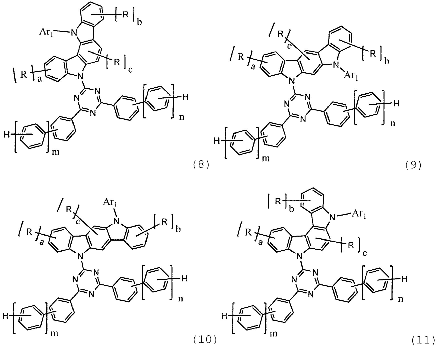
- formula (1) include formulae (6) to (11), and formula (6), (7), (8), or (9) is preferable, and formula (6) is more preferable.
- the light-emitting layer is a vapor deposition layer formed according to vacuum vapor deposition, and the first host and the second host are used by being mixed in advance before vapor deposition.
- a difference between 50% weight reduction temperatures of the first host and the second host is within 20°C, or a proportion of the first host is larger than 20 wt% and less than 55 wt% with respect to a total amount of the first host and the second host.
- the light-emitting dopant material can be a phosphorescent dopant material, a fluorescence-emitting dopant material or a thermally activated delayed fluorescence-emitting dopant material.
- the phosphorescent dopant material include an organic metal complex containing at least one metal selected from among ruthenium, rhodium, palladium, silver, rhenium, osmium, iridium, platinum and gold.
- a hole blocking layer adjacent to the light-emitting layer is provided, and the hole blocking layer contains a compound represented by formula (1).
- the present invention relates to a method of producing an organic electroluminescent element including a step of, when the above organic electroluminescent element is produced, mixing a first host and a second host to prepare a pre-mixture, and then vapor-depositing a host material containing the pre-mixture to form a light-emitting layer.
- the indolocarbazole compound of formula (1) has high framework stability and can control injection and transport properties of both charges to some extent according to isomers or substituents. However, it is difficult to independently control both amounts of charges injected and transported so that they are within a preferable range as described above.
- the biscarbazole compound of formula (2) can control charge injection and transport properties at a high level when types and the number of substituents thereof are changed.
- the biscarbazole compound has a higher lowest excited triplet energy than a biscarbazole compound in which a fused aromatic group is incorporated because a substituent other than a fused ring is incorporated on a nitrogen atom, and also has high amorphous stability, and has high framework stability like the indolocarbazole compound. Therefore, when a mixture of the indolocarbazole compound and the biscarbazole compound is used, an amount of charges injected into the organic layer can be adjusted to a preferable range, and more favorable element characteristics can be expected.
- a delayed fluorescence-emitting EL element or a phosphorescent EL element when a mixture of an indolocarbazole compound having at least one biphenyl group or terphenyl group on N or a triazine ring substituted on N and a biscarbazole compound having a phenylene group in which an aromatic hydrocarbon group is substituted on at least one N is used, the balance between charge injection and transport properties of holes and electrons is suitable, and also a lowest excited triplet energy sufficiently high to confine the excitation energy generated in the light-emitting layer is provided so that there is no outflow of energy from the inside of the light-emitting layer, and high efficiency and a prolonged lifespan can be obtained at a low voltage.
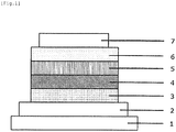
- Fig. 1 is a cross-sectional view schematically showing an example of an organic EL element.
- An organic EL element of the present invention has at least one light-emitting layer between an anode and a cathode which face each other and at least one of light-emitting layers includes a vapor deposition layer containing a first host, a second host, and a light-emitting dopant material.
- the vapor deposition layer can be produced according to vacuum vapor deposition.
- the first host is a compound represented by formula (1)
- the second host is a compound represented by formula (2).
- the organic EL element has a plurality of organic layers between an anode and a cathode which face each other, but at least one of the plurality of layers is a light-emitting layer, and a plurality of light-emitting layers may be provided.
- the ring A is an aromatic hydrocarbon ring represented by formula (1a)
- the ring B is a heterocycle represented by formula (1b)
- the ring A and the ring B are each fused to an adjacent ring at any position.
- Ar 1 represents a phenyl group, a biphenyl group, or a terphenyl group. Preferable examples thereof include a phenyl group or a biphenyl group, and more preferable examples thereof include a phenyl group.
- the biphenyl group is a group represented by -Ph-Ph
- the terphenyl group is a group represented by -Ph-Ph-Ph or Ph(-Ph)-Ph
- Ph is linked at any position (o-position, m-position, p-position).
- Ph is a phenyl group or a phenylene group.
- R each independently represents an aliphatic hydrocarbon group having 1 to 10 carbon atoms, an aromatic hydrocarbon group having 6 to 10 carbon atoms, or an aromatic heterocyclic group having 3 to 12 carbon atoms.
- Preferable examples thereof include an aliphatic hydrocarbon group having 1 to 8 carbon atoms, a phenyl group, and an aromatic heterocyclic group having 3 to 9 carbon atoms. More preferable examples thereof include an aliphatic hydrocarbon group having 1 to 6 carbon atoms, a phenyl group, and an aromatic heterocyclic group having 3 to 6 carbon atoms.
- aliphatic hydrocarbon group having 1 to 10 carbon atoms include methyl, ethyl, propyl, butyl, pentyl, hexyl, heptyl, octyl, nonyl, and decyl.
- An alkyl group having 1 to 4 carbon atoms is preferable.
- aromatic hydrocarbon group having 6 to 10 carbon atoms or the aromatic heterocyclic group having 3 to 12 carbon atoms include aromatic groups formed by taking one H from benzene, naphthalene, pyridine, pyrimidine, triazine, thiophene, isothiazole, thiazole, pyridazine, pyrrole, pyrazole, imidazole, triazole, thiadiazole, pyrazine, furan, isoxazole, oxazole, oxadiazole, quinoline, isoquinoline, quinoxaline, quinazoline, oxadiazole, thiadiazole, benzotriazine, phthalazine, tetrazole, indole, benzofuran, benzothiophene, benzoxazole, benzothiazole, indazole, benzimidazole, benzotriazole, benzoisothiazole, benzothiadia
- Preferable examples thereof include aromatic groups generated from benzene, pyridine, pyrimidine, triazine, thiophene, isothiazole, thiazole, pyridazine, pyrrole, pyrazole, imidazole, triazole, thiadiazole, pyrazine, furan, isoxazole, oxazole, oxadiazole, quinoline, isoquinoline, quinoxaline, quinazoline, oxadiazole, thiadiazole, benzotriazine, phthalazine, tetrazole, indole, benzofuran, benzothiophene, benzoxazole, benzothiazole, indazole, benzimidazole, benzotriazole, benzoisothiazole, or benzothiadiazole.
- More preferable examples thereof include aromatic groups generated from benzene, pyridine, pyrimidine, triazine, thiophene, isothiazole, thiazole, pyridazine, pyrrole, pyrazole, imidazole, triazole, thiadiazole, pyrazine, furan, isoxazole, oxazole, or oxadiazole.
- a, b, and c represent the number of substitutions, and each independently represents an integer of 0 to 3, and are preferably an integer of 0 or 1.
- m and n represent the number of repetitions, and each independently represents an integer of 0 to 2, and is preferably an integer of 0 or 1.
- m+n is preferably an integer of 0 or 1 or more, and more preferably an integer of 1, 2 or 3.
- Ar 1 is a phenyl group
- m+n is preferably an integer of 1 to 4, and more preferably an integer of 1, 2 or 3.
- formula (1) Preferable embodiments of formula (1) include formulae (6) to (11).
- symbols the same as those in formula (1) have the same meanings as in formula (1).
- Ar 2 and Ar 3 independently represent a hydrogen atom, an aromatic hydrocarbon group having 6 to 14 carbon atoms, or a group in which two of the aromatic hydrocarbon groups are linked (referred to as a linked aromatic group).
- a linked aromatic group Preferable examples thereof include a hydrogen atom and an aromatic hydrocarbon group having 6 to 12 carbon atoms, and more preferable examples thereof include an aromatic hydrocarbon group having 6 to 10 carbon atoms.
- Ar 2 is a hydrogen atom or Ar 2 is a hydrogen atom
- Ar 3 is the above aromatic hydrocarbon group or linked aromatic group.
- Ar 2 and Ar 3 are not both a hydrogen atom.
- Ar 2 and Ar 3 include a hydrogen atom, an aromatic hydrocarbon such as benzene, naphthalene, anthracene, phenanthrene, and fluorene, an aromatic group formed by taking one H from a compound in which two aromatic rings of such aromatic hydrocarbons are linked and a linked aromatic group.
- aromatic group generated from benzene, naphthalene, anthracene, or phenanthrene and a linked aromatic group in which two of these aromatic groups are linked
- Ar 3 is more preferably a phenyl group.
- Ar 2 and Ar 3 may be a hydrogen atom, and in this case, the other is the above aromatic group or linked aromatic group. More preferably, Ar 2 is a hydrogen atom and Ar 3 is a phenyl group.
- the above aromatic group or linked aromatic group may have a substituent, and a preferable substituent is an alkyl group having 1 to 12 carbon atoms or an alkoxy group having 1 to 12 carbon atoms.
- the linked aromatic group is represented by, for example, a formula of -Ar 4 -Ar 5 .
- Ar 4 and Ar 5 independently represent an aromatic hydrocarbon group having 6 to 14 carbon atoms.
- Ar 4 is a divalent or trivalent group, and
- Ar 5 is a monovalent group.
- Aromatic groups constituting the linked aromatic group may be the same as or different from each other.
- L 1 and L 2 are a phenylene group
- the phenylene group is a p-phenylene group or an m-phenylene group.
- the p-phenylene group and the m-phenylene group are represented by formula (2a) and formula (2b), respectively.
- the other -L 1 -Ar 2 or -L 2 -Ar 3 may be an m-phenylene group or a p-phenylene group in which an aromatic hydrocarbon group is substituted.
- L 1 is a phenylene group represented by formula (2a)
- L 2 is a phenylene group represented by formula (2b)
- Ar 2 is a hydrogen atom
- -L 1 -Ar 2 is a phenyl group
- L 2 is an m-phenylene group or a p-phenylene group.
- L 1 L 2 not be satisfied except for a case in which Ar 2 or Ar 3 is a hydrogen atom. That is, L 1 and L 2 are not both p-phenylene groups, and not both m-phenylene groups. For example, when one is a p-phenylene group, the other is an m-phenylene group.
- Ar 2 or Ar 3 is a hydrogen atom
- the first host and the second host which are vapor-deposited from different vapor deposition sources can be used. However, preferably, they are mixed in advance before vapor deposition to prepare a pre-mixture, and the pre-mixture is vapor-deposited from one vapor deposition source at the same time to form a light-emitting layer.
- a light-emitting dopant material necessary for forming a light-emitting layer or another host used as necessary may be mixed into the pre-mixture.
- vapor deposition may be performed from another vapor deposition source.
- a proportion of the first host is 20% to 60%, preferably more than 20% and less than 55%, and more preferably 40% to 50% with respect to a total amount of the first host and the second host.
- Fig. 1 is a cross-sectional view showing a structure example of an organic EL element generally used for the present invention.
- 1 indicates a substrate
- 2 indicates an anode
- 3 indicates a hole injection layer
- 4 indicates a hole transport layer
- 5 indicates a light-emitting layer
- 6 indicates an electron transport layer
- 7 indicates a cathode.
- the organic EL element of the present invention may have an exciton blocking layer adjacent to the light-emitting layer and may have an electron blocking layer between the light-emitting layer and the hole injection layer.
- the exciton blocking layer can be inserted into either on the side of the cathode or the cathode of the light-emitting layer and inserted into both sides at the same time.
- the organic EL element of the present invention has the anode, the light-emitting layer, and the cathode as essential layers, and may have a hole injection transport layer and an electron injection transport layer in addition to the essential layers, and may have additionally a hole blocking layer between the light-emitting layer and the electron injection transport layer.
- the hole injection transport layer refers to either or both of the hole injection layer and the hole transport layer
- the electron injection transport layer refers to either or both of the electron injection layer and the electron transport layer.
- a structure reverse to that of Fig. 1 that is, a structure in which a cathode 7, an electron transport layer 6, a light-emitting layer 5, a hole transport layer 4, and an anode 2 are laminated on a substrate 1 in this order, can be used, and in this case also, layers can be added or omitted as necessary.
- the organic EL element of the present invention is preferably supported on a substrate.
- the substrate is not particularly limited, and those used in the organic EL element in the related art may be used, and those made of, for example, glass, a transparent plastic, or quartz, can be used.
- anode material for an organic EL element a material of a metal having a large work function (4 eV or more), an alloy, an electrically conductive compound or a mixture thereof is preferably used.
- an electrode material include a metal such as Au, and a conductive transparent material such as CuI, indium tin oxide (ITO), SnO 2 , and ZnO.
- an amorphous material such as IDIXO (In 2 O 3 -ZnO) which can form a transparent conductive film may be used.
- anode such an electrode material is used to form a thin film by a vapor-deposition or sputtering method, and a desired shape pattern may be formed by a photolithographic method, or if the pattern accuracy is not particularly required (about 100 ⁇ m or more), a pattern may be formed via a desired shape mask when the electrode material is vapor-deposited or sputtered.
- a coatable substance such as the organic conductive compound
- a wet film formation method such as a printing method and a coating method can be used.
- the transmittance be larger than 10% and sheet resistance for the anode is preferably several hundreds ⁇ /sq or less.
- the film thickness depends on the material, and it is generally 10 to 1,000 nm, and preferably selected in a range of 10 to 200 nm.
- a cathode material a material of a metal having a small work function (4 eV or less) (an electron injection metal), an alloy, an electrically conductive compound, or a mixture thereof is used.
- an electrode material include sodium, a sodium-potassium alloy, magnesium, lithium, a magnesium/copper mixture, a magnesium/silver mixture, a magnesium/aluminum mixture, a magnesium/indium mixture, an aluminum/aluminum oxide (Al 2 O 3 ) mixture, indium, a lithium/aluminum mixture, and a rare earth metal.
- a mixture of an electron injection metal and a second metal which is a stable metal having a larger work function value for example, a magnesium/silver mixture, a magnesium/aluminum mixture, a magnesium/indium mixture, an aluminum/aluminum oxide mixture, a lithium/aluminum mixture, aluminum, and the like are suitable.
- the cathode can be produced by forming a thin film by a method such as vapor-depositing or sputtering of such a cathode material.
- sheet resistance for the cathode is preferably several hundreds ⁇ /sq or less, and the film thickness is generally 10 nm to 5 ⁇ m, and preferably selected in a range of 50 to 200 nm.
- the film thickness is generally 10 nm to 5 ⁇ m, and preferably selected in a range of 50 to 200 nm.
- a transparent or translucent cathode can be produced and by applying this, it is possible to produce an element in which both the anode and the cathode have transparency.
- the light-emitting layer is a layer that emits light after excitons are generated when holes and electrons injected from the anode and the cathode, respectively, are recombined.
- an organic light-emitting dopant material and a host material are included.
- the first host represented by formula (1) and the second host represented by formula (2) are used.
- one or more types of known host materials may be used in combination, and an amount used is 50 wt% or less, and preferably 25 wt% or less with respect to a total amount of host materials.
- the first host and the second host are vapor-deposited from different vapor deposition sources. However, they are mixed in advance before vapor deposition to prepare a pre-mixture, and thus the first host and the second host can be vapor-deposited from one vapor deposition source at the same time.
- the 50% weight reduction temperature is a temperature at which the weight is reduced by 50% when the temperature is raised to 550°C from room temperature at a rate of 10°C/min in TG-DTA measurement under a nitrogen stream reduced pressure (50 Pa). Vaporization due to evaporation or sublimation is considered most likely to occur around this temperature.
- the difference between 50% weight reduction temperatures of the first host and the second host is preferably within 20°C and more preferably within 15°C.
- a premixing method a known method such as pulverization and mixing can be used, and it is desirable to mix them as uniformly as possible.
- a phosphorescent dopant including an organic metal complex containing at least one metal selected from among ruthenium, rhodium, palladium, silver, rhenium, osmium, iridium, platinum, and gold may be used.
- organic metal complex containing at least one metal selected from among ruthenium, rhodium, palladium, silver, rhenium, osmium, iridium, platinum, and gold may be used.
- iridium complexes described in J. Am. Chem. Soc. 2001, 123, 4304 and Japanese Translation of PCT Application No. 2013-53051 are preferably used, but the present invention is not limited thereto.
- a content of the phosphorescent dopant material is preferably 0.1 to 30 wt% and more preferably 1 to 20 wt% with respect to the host material.
- the phosphorescent dopant material is not particularly limited, and specific examples thereof include the following.
- the fluorescence-emitting dopant is not particularly limited.
- examples thereof include benzoxazole derivatives, benzothiazole derivatives, benzimidazole derivatives, styrylbenzene derivatives, polyphenyl derivatives, diphenylbutadiene derivatives, tetraphenyl butadiene derivatives, naphthalimido derivatives, coumarin derivatives, fused aromatic compounds, perinone derivatives, oxadiazole derivatives, oxazine derivatives, aldazine derivatives, pyrrolidine derivatives, cyclopentadiene derivatives, bisstyryl anthracene derivatives, quinacridone derivatives, pyrrolopyridine derivatives, thiadiazolopyridine derivatives, styrylamine derivatives, diketopyrrolopyrrole derivatives, aromatic dimethylidine compounds, metal complexe
- Preferable examples thereof include fused aromatic derivatives, styryl derivatives, diketopyrrolopyrrole derivatives, oxazine derivatives, pyromethene metal complexes, transition metal complexes, and lanthanoid complexes.
- More preferable examples thereof include naphthalene, pyrene, chrysene, triphenylene, benzo[c]phenanthrene, benzo[a]anthracene, pentacene, perylene, fluoranthene, acenaphthofluoranthene, dibenzo[a,j]anthracene, dibenzo[a,h]anthracene, benzo[a]naphthalene, hexacene, naphtho[2,1-f]isoquinoline, ⁇ -naphthaphenanthridine, phenanthrooxazole, quinolino[6,5-f]quinoline, and benzothiophanthrene. These may have an alkyl group, an aryl group, an aromatic heterocyclic group, or a diarylamino group as a substituent.
- a fluorescence-emitting dopant material may be contained in the light-emitting layer or two or more types thereof may be contained.
- a content of the fluorescence-emitting dopant material is preferably 0.1% to 20% and more preferably 1% to 10% with respect to the host material.
- the thermally activated delayed fluorescence-emitting dopant is not particularly limited.
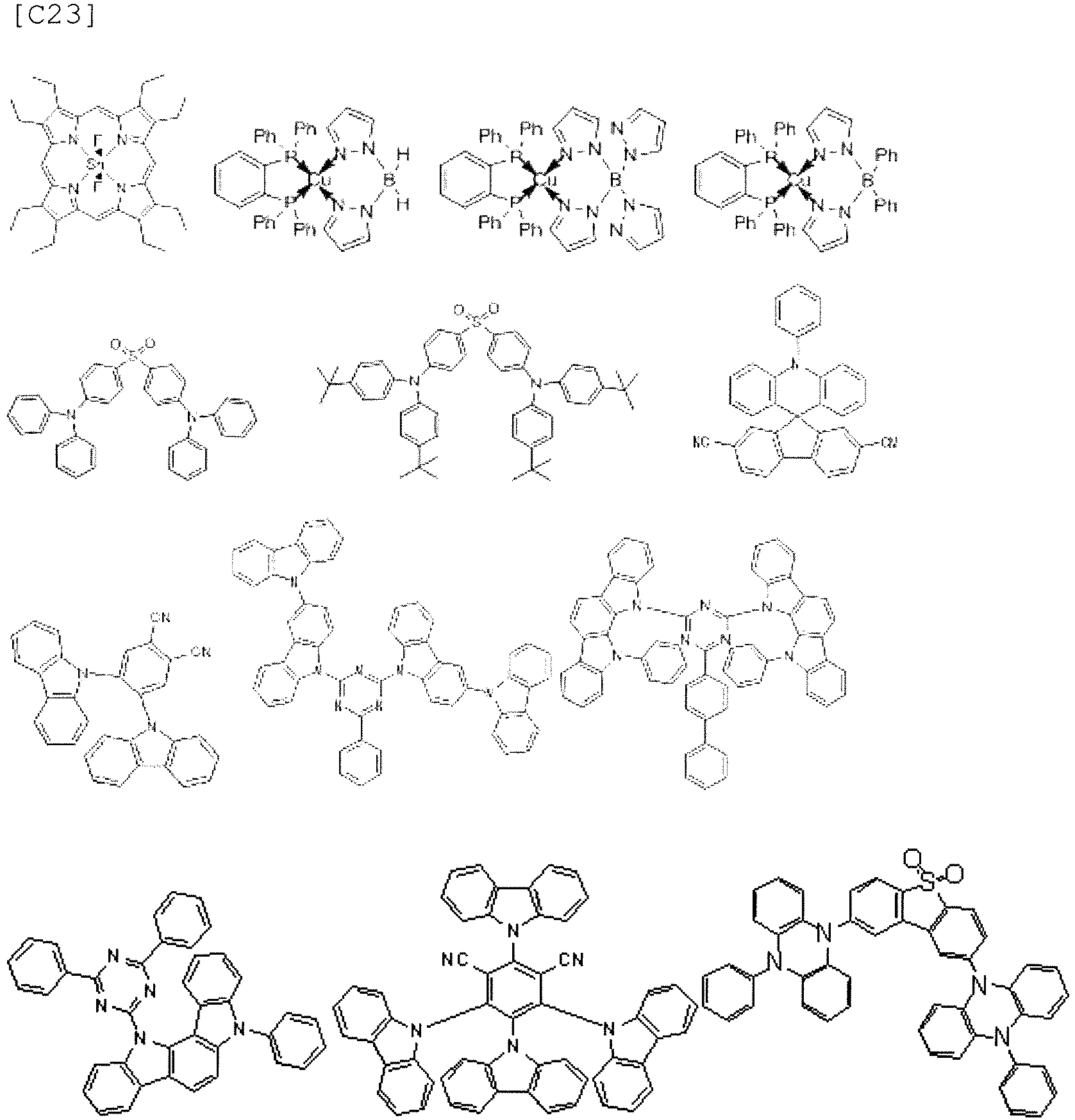
- examples thereof include metal complexes such as a tin complex and a copper complex, indolocarbazole derivatives described in WO 2011/070963 , cyanobenzene derivatives and carbazole derivatives described in Nature 2012, 492, 234 , and phenazine derivatives, oxadiazole derivatives, triazole derivatives, sulfone derivatives, phenoxazine derivatives, and acridine derivatives described in Nature Photonics 2014, 8, 326 .
- the thermally activated delayed fluorescence-emitting dopant material is not particularly limited, and specific examples thereof include the following.
- thermally activated delayed fluorescence-emitting dopant material Only one type of a thermally activated delayed fluorescence-emitting dopant material may be contained in the light-emitting layer or two or more types thereof may be contained.
- the thermally activated delayed fluorescence-emitting dopant may be used in a combination of a phosphorescent dopant and a fluorescence-emitting dopant.
- a content of the thermally activated delayed fluorescence-emitting dopant material is preferably 0.1% to 50% and more preferably 1% to 30% with respect to the host material.
- the injection layer is a layer that is provided between an electrode and an organic layer in order to lower a driving voltage and improve light emission brightness, and includes a hole injection layer and an electron injection layer, and may be present between the anode and the light-emitting layer or the hole transport layer, and between the cathode and the light-emitting layer or the electron transport layer.
- the injection layer can be provided as necessary.
- the hole blocking layer has a function of the electron transport layer in a broad sense, and is made of a hole blocking material having a function of transporting electrons and a significantly low ability to transport holes, and can block holes while transporting electrons, and thus can improve a probability of recombining electrons and holes in the light-emitting layer.
- a known hole blocking layer material can be used for the hole blocking layer, and an indolocarbazole compound is preferably contained. Any indolocarbazole compound may be used as long as it has one or more indolocarbazole rings.
- the indolocarbazole ring is a ring in which 5 rings are fused in formula (1).
- the electron blocking layer has a function of a hole transport layer in a broad sense and blocks electrons while transporting holes, and thus can improve a probability of recombining electrons and holes in the light-emitting layer.
- the film thickness of the electron blocking layer is preferably 3 to 100 nm, and more preferably 5 to 30 nm.
- the exciton blocking layer is a layer for blocking diffusion of excitons generated when holes and electrons are recombined in the light-emitting layer in a charge transport layer, and when this layer is inserted, excitons can be efficiently confined in the light-emitting layer, and the luminous efficiency of the element can be improved.
- the exciton blocking layer can be inserted between two adjacent light-emitting layers in an element in which two or more light-emitting layers are adjacent to each other.
- exciton blocking layer a known exciton blocking layer material can be used.
- exciton blocking layer material examples thereof include 1,3-dicarbazolyl benzene (mCP) and bis(2-methyl-8-quinolinolato)-4-phenylphenolato aluminum(III) (BAlq) .
- the hole transport layer is made of a hole transport material having a function of transporting holes, and a single hole transport layer or a plurality of hole transport layers can be provided.
- the hole transport material has either hole injection or transport properties or electron barrier properties, and may be an organic material or an inorganic material.
- any one selected from among conventionally known compounds can be used.
- Examples of such a hole transport material include porphyrin derivatives, arylamine derivatives, triazole derivatives, oxadiazole derivatives, imidazole derivatives, polyarylalkane derivatives, pyrazoline derivatives, pyrazolone derivatives, phenylenediamine derivatives, arylamine derivatives, amino-substituted chalcone derivatives, oxazole derivatives, styryl anthracene derivatives, fluorenone derivatives, hydrazone derivatives, stilbene derivatives, silazane derivatives, an aniline copolymer, and a conductive polymer oligomer, and particularly a thiophene oligomer.
- Porphyrin derivatives, arylamine derivatives, or styrylamine derivatives are
- the electron transport layer is made of a material having a function of transporting electrons, and a single electron transport layer or a plurality of electron transport layers can be provided.
- the electron transport material (which may also be a hole blocking material) may have a function of transferring electrons injected from the cathode to the light-emitting layer.
- the electron transport layer any one selected from among conventionally known compounds can be used, and examples thereof include polycyclic aromatic derivatives such as naphthalene, anthracene, and phenanthroline, tris(8-quinolinolato)aluminum(III) derivatives, phosphine oxide derivatives, nitro-substituted fluorene derivatives, diphenylquinone derivatives, thiopyrandioxide derivatives, carbodiimide, freorenylidene methane derivatives, anthraquinodimethane and anthrone derivatives, bipyridine derivatives, quinoline derivatives, oxadiazole derivatives, benzimidazole derivatives, benzothiazole derivatives, and indolocarbazole derivatives.
- Pre-mixtures H2 to H15 were prepared using first hosts and second hosts shown in Table 1.
- Table 2 shows the 50% weight reduction temperature (T 50 ) of Compounds 1-2, 1-5, 1-7, 1-10, 1-15, 1-109, 2-1, 2-2, and 2-3 and Compounds A, B, and C.
- T 50 50% weight reduction temperature
- HAT-CN was formed with a thickness of 25 nm as a hole injection layer on ITO, and next NPD was formed with a thickness of 30 nm as a hole transport layer.
- HT-1 was formed with a thickness of 10 nm as an electron blocking layer.
- Pre-mixture H1 as a host and Ir(ppy) 3 as a light-emitting dopant were co-vapor-deposited from different vapor deposition sources to form a light-emitting layer with a thickness of 40 nm.
- co-vapor-deposition was performed under vapor deposition conditions such that the concentration of Ir(ppy) 3 was 10 wt%.
- ET-1 was formed with a thickness of 20 nm as an electron transport layer.
- lithium fluoride (LiF) was formed with a thickness of 1 nm as an electron injection layer on the electron transport layer.
- aluminum (Al) was formed with a thickness of 70 nm as a cathode on the electron injection layer to produce an organic EL element.
- Organic EL elements were produced in the same manner as in Example 1 except that any of Pre-mixtures H2 to H15 was used as the host in Example 1.
- An organic EL element was produced in the same manner as in Example 1 except that, in Example 1, a light-emitting layer was formed using Pre-mixture H1 as a host and Ir(ppy) 3 as a light-emitting dopant, and Compound C was then formed with a thickness of 10 nm as a hole blocking layer on the light-emitting layer, and next ET-1 was formed with a thickness of 10 nm as the electron transport layer.
- Organic EL elements were produced in the same manner as in Example 16 except that any of Pre-mixtures H3, H7, H9, and H11 was used as the host in Example 16.
- the brightness, driving voltage, luminous efficiency, and lifespan characteristics of the produced organic EL elements are shown in Tables 3 to 7.
- the brightness, driving voltage, and luminous efficiency were values at a drive current of 20 mA/cm 2 and were initial characteristics.
- LT70 was a time taken for the brightness to be reduced to 70% of the initial brightness when the initial brightness was 9,000 cd/m 2
- LT95 was a time taken for the brightness to be reduced to 95% of the initial brightness when the initial brightness was 3,700 cd/m 2 , and both are lifespan characteristics.
- HAT-CN was formed with a thickness of 25 nm as a hole injection layer on ITO, and next NPD was formed with a thickness of 30 nm as a hole transport layer.
- HT-1 was formed with a thickness of 10 nm as an electron blocking layer.
- Compound 1-2 as a first host, Compound 2-1 as a second host, and Ir(ppy) 3 as a light-emitting dopant were co-vapor-deposited from different vapor deposition sources to form a light-emitting layer with a thickness of 40 nm.
- co-vapor-deposition was performed under vapor deposition conditions such that the concentration of Ir(ppy) 3 was 10 wt%, and the weight ratio between the first host and the second host was 30:70.
- ET-1 was formed with a thickness of 20 nm as an electron transport layer.
- LiF was formed with a thickness of 1 nm as an electron injection layer on the electron transport layer.
- Al was formed with a thickness of 70 nm as a cathode on the electron injection layer to produce an organic EL element.
- Organic EL elements were produced in the same manner as in Example 21 except that compounds shown in Table 4 were used as the first host and the second host in Example 21.
- Organic EL elements were produced in the same manner as in Examples 21 to 23 except that a light-emitting layer was formed, Compound C was then formed with a thickness of 10 nm as a hole blocking layer, and ET-1 was formed with a thickness of 10 nm as an electron transport layer in Examples 21 to 23.
- HAT-CN was formed with a thickness of 25 nm as a hole injection layer on ITO, and next NPD was formed with a thickness of 45 nm as a hole transport layer.
- HT-1 was formed with a thickness of 10 nm as an electron blocking layer.
- Pre-mixture H1 as a host and Ir(piq) 2 acac as a light-emitting dopant were co-vapor-deposited from different vapor deposition sources to form a light-emitting layer with a thickness of 40 nm.
- co-vapor-deposition was performed under vapor deposition conditions such that the concentration of Ir(piq) 2 acac was 6.0 wt%.
- ET-1 was formed with a thickness of 37.5 nm as an electron transport layer.
- LiF was formed with a thickness of 1 nm as an electron injection layer on the electron transport layer.
- Al was formed with a thickness of 70 nm as a cathode on the electron injection layer to produce an organic EL element.
- Organic EL elements were produced in the same manner as in Example 43 except that any of Pre-mixtures H3, H7, H9, and H11 was used as the host in Example 43.
- Organic EL elements were produced in the same manner as in Examples 43 to 47 except that a light-emitting layer was formed, Compound C was then formed with a thickness of 10 nm as a hole blocking layer, and ET-1 was formed with a thickness of 10 nm as an electron transport layer in Examples 43 to 47.
- HAT-CN was formed with a thickness of 25 nm as a hole injection layer on ITO, and next NPD was formed with a thickness of 45 nm as a hole transport layer.
- HT-1 was formed with a thickness of 10 nm as an electron blocking layer.
- Compound 1-2 as a first host, Compound 2-1 as a second host, and Ir(piq) 2 acac as a light-emitting dopant were co-vapor-deposited from different vapor deposition sources to form a light-emitting layer with a thickness of 40 nm.
- co-vapor-deposition was performed under vapor deposition conditions such that the concentration of Ir(piq) 2 acac was 6.0 wt%, and the weight ratio between the first host and the second host was 50:50.
- ET-1 was formed with a thickness of 37.5 nm as an electron transport layer.
- LiF was formed with a thickness of 1 nm as an electron injection layer on the electron transport layer.
- Al was formed with a thickness of 70 nm as a cathode on the electron injection layer to produce an organic EL element.
- Organic EL elements were produced in the same manner as in Example 53 except that compounds shown in Table 6 were used as first hosts and second hosts in Example 53.
- Organic EL elements were produced in the same manner as in Examples 53 to 55 except that a light-emitting layer was formed, Compound C was then formed with a thickness of 10 nm as a hole blocking layer, and ET-1 was formed with a thickness of 10 nm as an electron transport layer in Examples 53 to 55.
- An organic EL element was produced in the same manner as in Example 1 except that Compound 1-2 alone was used as the host in Example 1.
- the thickness of the light-emitting layer and the light-emitting dopant concentration were the same as those in Example 1.
- Organic EL elements were produced in the same manner as in Comparative Example 1 except that compounds alone shown in Table 7 were used as the host.
- Organic EL elements were produced in the same manner as in Example 21 except that Compound 1-2 was used as a first host and Compound A or Compound B was used as a second host in Example 21.
- Organic EL elements were produced in the same manner as in Example 21 except that Compound C was used as a first host and Compound A, 2-1, 2-2, or 2-3 was used as a second host in Example 21.
- Organic EL elements were produced in the same manner as in Example 53 except that Compound 1-2 was used as a first host and Compound A or Compound B was used as a second host in Example 53.
- the organic EL element of the present invention has a low driving voltage, high efficiency, and high driving stability.
Landscapes
- Chemical & Material Sciences (AREA)
- Engineering & Computer Science (AREA)
- Materials Engineering (AREA)
- Physics & Mathematics (AREA)
- Spectroscopy & Molecular Physics (AREA)
- Crystallography & Structural Chemistry (AREA)
- Inorganic Chemistry (AREA)
- Organic Chemistry (AREA)
- Optics & Photonics (AREA)
- Manufacturing & Machinery (AREA)
- Electroluminescent Light Sources (AREA)
Abstract
Description
- The present invention relates to an organic electroluminescent element (referred to as an organic EL element), and specifically, to an organic EL element comprising a light-emitting layer containing a first host, a second host, and a light-emitting dopant material.
- When a voltage is applied to an organic EL element, holes are injected from an anode and electrons are injected from a cathode to a light-emitting layer. Thus, in the light-emitting layer, injected holes and electrons recombine to generate excitons. In this case, according to statistical rules of electron spins, singlet excitons and triplet excitons are generated at a ratio of 1:3. It is said that the internal quantum efficiency of a fluorescence-emitting organic EL element using light emission from singlet excitons is limited to 25%. Meanwhile, it has been known that, in a phosphorescent organic EL element using light emission from triplet excitons, when intersystem crossing is efficiently performed from singlet excitons, the internal quantum efficiency is raised to 100%.
- However, for phosphorescent organic EL elements, prolonging the lifespan is a technical issue.
- In addition, recently, organic EL elements using delayed fluorescence and having high efficiency have been developed. For example,
PTL 1 discloses an organic EL element using a triplet-triplet fusion (TTF) mechanism which is one of delayed fluorescence mechanisms. The TTF mechanism utilizes a phenomenon in which singlet excitons are generated due to collision of two triplet excitons, and it is thought that the internal quantum efficiency can theoretically be raised to 40%. However, since the efficiency is lower compared to phosphorescent organic EL elements, further improvement in efficiency is required. -
PTL 2 discloses an organic EL element using a thermally activated delayed fluorescence (TADF) mechanism. The TADF mechanism utilizes a phenomenon in which reverse intersystem crossing from triplet excitons to singlet excitons is generated in a material having a small energy difference between a singlet level and a triplet level, and it is thought that the internal quantum efficiency can theoretically be raised to 100%. However, further improvement in lifespan characteristics is required as in the case of phosphorescent elements. -
- [PTL 1]
WO 2010/134350 A - [PTL 2]
WO 2011/070963 A - [PTL 3]
WO 2008/056746 A - [PTL 4]
JP 2003-133075 A - [PTL 5]
WO 2013/062075 A - [PTL 6]
US 2014/0374728 A - [PTL 7]
US 2014/0197386 A - [PTL 8]
US 2015/0001488 A - [PTL 9]
US 2015/0236262 A - [PTL 10]
WO 2016/194604 A - [PTL 11]
WO 2011/136755 A -
PTL 3 discloses use of an indolocarbazole compound as a host material.PTL 4 discloses use of a biscarbazole compound as a host material. -
PTL PTL 7, 8, 9, and 10 disclose use of an indolocarbazole compound and a biscarbazole compound as a mixed host. - PTL 11 discloses use of a host material in which a plurality of hosts containing an indolocarbazole compound are premixed.
- However, none of these can be said to be sufficient, and further improvement is desired.
- In order to apply an organic EL element to a display element such as a flat panel display or a light source, it is necessary to improve the luminous efficiency of the element and to sufficiently secure stability during driving at the same time. An object of the present invention is to provide an organic EL element having high efficiency and high driving stability despite having a low driving voltage.
- The present invention relates to an organic EL element comprising one or more light-emitting layer between an anode and a cathode which face each other, wherein at least one light-emitting layer contains a first host selected from among compounds represented by the following formula (1), a second host selected from among compounds represented by the following formula (2), and a light-emitting dopant material.
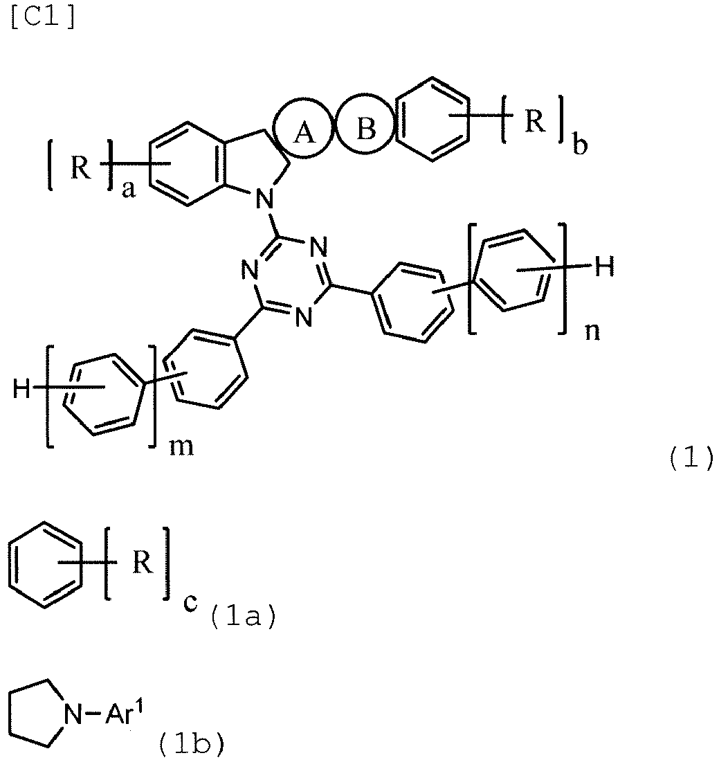
- (here, the ring A is an aromatic hydrocarbon ring represented by formula (1a), the ring B is a heterocycle represented by formula (1b), and the ring A and the ring B are each fused to an adjacent ring at any position,
- Ar1 represents a phenyl group, a biphenyl group or a terphenyl group,
- R each independently represents an aliphatic hydrocarbon group having 1 to 10 carbon atoms, an aromatic hydrocarbon group having 6 to 10 carbon atoms, or an aromatic heterocyclic group having 3 to 12 carbon atoms,
- a, b, and c represent the number of substitutions and each independently represents an integer of 0 to 3, and m and n represent the number of repetitions, and each independently represents an integer of 0 to 2, and preferably, when Ar1 is a phenyl group, m+n is an integer of 1 to 4).
- Preferable embodiments of formula (2) include formulae (3) to (5), and formula (4) or (5) is more preferable.

- Preferable embodiments of formula (1) include formulae (6) to (11), and formula (6), (7), (8), or (9) is preferable, and formula (6) is more preferable.

- Preferably, the light-emitting layer is a vapor deposition layer formed according to vacuum vapor deposition, and the first host and the second host are used by being mixed in advance before vapor deposition. In addition, preferably, a difference between 50% weight reduction temperatures of the first host and the second host is within 20°C, or a proportion of the first host is larger than 20 wt% and less than 55 wt% with respect to a total amount of the first host and the second host.
- The light-emitting dopant material can be a phosphorescent dopant material, a fluorescence-emitting dopant material or a thermally activated delayed fluorescence-emitting dopant material. Examples of the phosphorescent dopant material include an organic metal complex containing at least one metal selected from among ruthenium, rhodium, palladium, silver, rhenium, osmium, iridium, platinum and gold.
- In addition, preferably, in the organic EL element, a hole blocking layer adjacent to the light-emitting layer is provided, and the hole blocking layer contains a compound represented by formula (1).
- In addition, the present invention relates to a method of producing an organic electroluminescent element including a step of, when the above organic electroluminescent element is produced, mixing a first host and a second host to prepare a pre-mixture, and then vapor-depositing a host material containing the pre-mixture to form a light-emitting layer.
- In order to improve element characteristics, it is necessary to increase durability of a material used for an organic layer against charges, and particularly, in the light-emitting layer, it is important to reduce leakage of excitons and charges to surrounding layers. In order to reduce leakage of charges/excitons, alleviating deviation of a light emission area in the light-emitting layer is effective. For this, it is necessary to control both amounts of charges (electrons/holes) injected into the light-emitting layer and both amounts of charges transported in the light-emitting layer such that they are within a preferable range.
- Here, the indolocarbazole compound of formula (1) has high framework stability and can control injection and transport properties of both charges to some extent according to isomers or substituents. However, it is difficult to independently control both amounts of charges injected and transported so that they are within a preferable range as described above. On the other hand, the biscarbazole compound of formula (2) can control charge injection and transport properties at a high level when types and the number of substituents thereof are changed. In addition, the biscarbazole compound has a higher lowest excited triplet energy than a biscarbazole compound in which a fused aromatic group is incorporated because a substituent other than a fused ring is incorporated on a nitrogen atom, and also has high amorphous stability, and has high framework stability like the indolocarbazole compound. Therefore, when a mixture of the indolocarbazole compound and the biscarbazole compound is used, an amount of charges injected into the organic layer can be adjusted to a preferable range, and more favorable element characteristics can be expected. In particular, in the case of a delayed fluorescence-emitting EL element or a phosphorescent EL element, when a mixture of an indolocarbazole compound having at least one biphenyl group or terphenyl group on N or a triazine ring substituted on N and a biscarbazole compound having a phenylene group in which an aromatic hydrocarbon group is substituted on at least one N is used, the balance between charge injection and transport properties of holes and electrons is suitable, and also a lowest excited triplet energy sufficiently high to confine the excitation energy generated in the light-emitting layer is provided so that there is no outflow of energy from the inside of the light-emitting layer, and high efficiency and a prolonged lifespan can be obtained at a low voltage.
- [
Fig. 1] Fig. 1 is a cross-sectional view schematically showing an example of an organic EL element. - An organic EL element of the present invention has at least one light-emitting layer between an anode and a cathode which face each other and at least one of light-emitting layers includes a vapor deposition layer containing a first host, a second host, and a light-emitting dopant material. The vapor deposition layer can be produced according to vacuum vapor deposition. The first host is a compound represented by formula (1), and the second host is a compound represented by formula (2). The organic EL element has a plurality of organic layers between an anode and a cathode which face each other, but at least one of the plurality of layers is a light-emitting layer, and a plurality of light-emitting layers may be provided.
- Formula (1) will be described.
- The ring A is an aromatic hydrocarbon ring represented by formula (1a), the ring B is a heterocycle represented by formula (1b), and the ring A and the ring B are each fused to an adjacent ring at any position.
- Ar1 represents a phenyl group, a biphenyl group, or a terphenyl group. Preferable examples thereof include a phenyl group or a biphenyl group, and more preferable examples thereof include a phenyl group. Here, the biphenyl group is a group represented by -Ph-Ph, the terphenyl group is a group represented by -Ph-Ph-Ph or Ph(-Ph)-Ph, and Ph is linked at any position (o-position, m-position, p-position). Here, Ph is a phenyl group or a phenylene group.
- R each independently represents an aliphatic hydrocarbon group having 1 to 10 carbon atoms, an aromatic hydrocarbon group having 6 to 10 carbon atoms, or an aromatic heterocyclic group having 3 to 12 carbon atoms. Preferable examples thereof include an aliphatic hydrocarbon group having 1 to 8 carbon atoms, a phenyl group, and an aromatic heterocyclic group having 3 to 9 carbon atoms. More preferable examples thereof include an aliphatic hydrocarbon group having 1 to 6 carbon atoms, a phenyl group, and an aromatic heterocyclic group having 3 to 6 carbon atoms.
- Specific examples of the aliphatic hydrocarbon group having 1 to 10 carbon atoms include methyl, ethyl, propyl, butyl, pentyl, hexyl, heptyl, octyl, nonyl, and decyl. An alkyl group having 1 to 4 carbon atoms is preferable.
- Specific examples of the aromatic hydrocarbon group having 6 to 10 carbon atoms or the aromatic heterocyclic group having 3 to 12 carbon atoms include aromatic groups formed by taking one H from benzene, naphthalene, pyridine, pyrimidine, triazine, thiophene, isothiazole, thiazole, pyridazine, pyrrole, pyrazole, imidazole, triazole, thiadiazole, pyrazine, furan, isoxazole, oxazole, oxadiazole, quinoline, isoquinoline, quinoxaline, quinazoline, oxadiazole, thiadiazole, benzotriazine, phthalazine, tetrazole, indole, benzofuran, benzothiophene, benzoxazole, benzothiazole, indazole, benzimidazole, benzotriazole, benzoisothiazole, benzothiadiazole, dibenzofuran, dibenzothiophene, dibenzoselenophene, or carbazole. Preferable examples thereof include aromatic groups generated from benzene, pyridine, pyrimidine, triazine, thiophene, isothiazole, thiazole, pyridazine, pyrrole, pyrazole, imidazole, triazole, thiadiazole, pyrazine, furan, isoxazole, oxazole, oxadiazole, quinoline, isoquinoline, quinoxaline, quinazoline, oxadiazole, thiadiazole, benzotriazine, phthalazine, tetrazole, indole, benzofuran, benzothiophene, benzoxazole, benzothiazole, indazole, benzimidazole, benzotriazole, benzoisothiazole, or benzothiadiazole. More preferable examples thereof include aromatic groups generated from benzene, pyridine, pyrimidine, triazine, thiophene, isothiazole, thiazole, pyridazine, pyrrole, pyrazole, imidazole, triazole, thiadiazole, pyrazine, furan, isoxazole, oxazole, or oxadiazole.
- a, b, and c represent the number of substitutions, and each independently represents an integer of 0 to 3, and are preferably an integer of 0 or 1. m and n represent the number of repetitions, and each independently represents an integer of 0 to 2, and is preferably an integer of 0 or 1. Here, m+n is preferably an integer of 0 or 1 or more, and more preferably an integer of 1, 2 or 3. Here, when Ar1 is a phenyl group, m+n is preferably an integer of 1 to 4, and more preferably an integer of 1, 2 or 3.
- Preferable embodiments of formula (1) include formulae (6) to (11). In formulae (6) to (11), symbols the same as those in formula (1) have the same meanings as in formula (1).
- Specific examples of compounds represented by formula (1) are shown below, but the present invention is not limited to such exemplary compounds.


- Next, formula (2) representing the second host and formulae (3) to (5) which represent preferable embodiments thereof will be described. In formulae (2) to (5), the same symbols have the same meanings.
- Ar2 and Ar3 independently represent a hydrogen atom, an aromatic hydrocarbon group having 6 to 14 carbon atoms, or a group in which two of the aromatic hydrocarbon groups are linked (referred to as a linked aromatic group). Preferable examples thereof include a hydrogen atom and an aromatic hydrocarbon group having 6 to 12 carbon atoms, and more preferable examples thereof include an aromatic hydrocarbon group having 6 to 10 carbon atoms. In a preferable embodiment, Ar2 is a hydrogen atom or Ar2 is a hydrogen atom, and Ar3 is the above aromatic hydrocarbon group or linked aromatic group. However, Ar2 and Ar3 are not both a hydrogen atom.
- Specific examples of Ar2 and Ar3 include a hydrogen atom, an aromatic hydrocarbon such as benzene, naphthalene, anthracene, phenanthrene, and fluorene, an aromatic group formed by taking one H from a compound in which two aromatic rings of such aromatic hydrocarbons are linked and a linked aromatic group. Preferable examples thereof include an aromatic group generated from benzene, naphthalene, anthracene, or phenanthrene, and a linked aromatic group in which two of these aromatic groups are linked, and more preferable examples thereof include an aromatic group generated from benzene, naphthalene, or phenanthrene. Ar3 is more preferably a phenyl group. One of Ar2 and Ar3 may be a hydrogen atom, and in this case, the other is the above aromatic group or linked aromatic group. More preferably, Ar2 is a hydrogen atom and Ar3 is a phenyl group. In addition, the above aromatic group or linked aromatic group may have a substituent, and a preferable substituent is an alkyl group having 1 to 12 carbon atoms or an alkoxy group having 1 to 12 carbon atoms.
- Here, the linked aromatic group is represented by, for example, a formula of -Ar4-Ar5. Here, Ar4 and Ar5 independently represent an aromatic hydrocarbon group having 6 to 14 carbon atoms. Ar4 is a divalent or trivalent group, and Ar5 is a monovalent group. Aromatic groups constituting the linked aromatic group may be the same as or different from each other.
- L1 and L2 are a phenylene group, and the phenylene group is a p-phenylene group or an m-phenylene group. The p-phenylene group and the m-phenylene group are represented by formula (2a) and formula (2b), respectively. Thus, when one Ar2 or Ar3 is a hydrogen atom, the other -L1-Ar2 or -L2-Ar3 may be an m-phenylene group or a p-phenylene group in which an aromatic hydrocarbon group is substituted.
- Preferably, L1 is a phenylene group represented by formula (2a), L2 is a phenylene group represented by formula (2b), Ar2 is a hydrogen atom, -L1-Ar2 is a phenyl group, and L2 is an m-phenylene group or a p-phenylene group. In another aspect, it is preferable that L1=L2 not be satisfied except for a case in which Ar2 or Ar3 is a hydrogen atom. That is, L1 and L2 are not both p-phenylene groups, and not both m-phenylene groups. For example, when one is a p-phenylene group, the other is an m-phenylene group. When one Ar2 or Ar3 is a hydrogen atom, a case in which L1=L2 is satisfied is excluded because a substitution position for L1 or L2 is an arbitrary phenylene group.
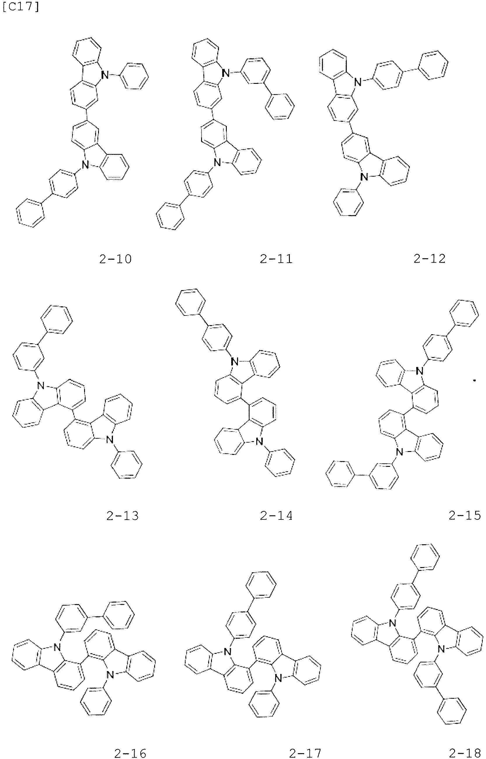
- Specific examples of compounds represented by formulae (2) to (5) are shown below, but the present invention is not limited to such exemplary compounds.





- It is possible to provide an excellent organic EL element using the first host selected from among compounds represented by formula (1) and the second host selected from among compounds represented by formula (2) as host materials of a light-emitting layer.
- The first host and the second host which are vapor-deposited from different vapor deposition sources can be used. However, preferably, they are mixed in advance before vapor deposition to prepare a pre-mixture, and the pre-mixture is vapor-deposited from one vapor deposition source at the same time to form a light-emitting layer. In this case, a light-emitting dopant material necessary for forming a light-emitting layer or another host used as necessary may be mixed into the pre-mixture. However, when there is a large difference in temperature at which a desired vapor pressure is obtained, vapor deposition may be performed from another vapor deposition source.
- In addition, regarding the mixing ratio (weight ratio) between the first host and the second host, a proportion of the first host is 20% to 60%, preferably more than 20% and less than 55%, and more preferably 40% to 50% with respect to a total amount of the first host and the second host.
- Next, the structure of the organic EL element of the present invention will be described with reference to the drawing, but the structure of the organic EL element of the present invention is not limited thereto.
-
Fig. 1 is a cross-sectional view showing a structure example of an organic EL element generally used for the present invention. 1 indicates a substrate, 2 indicates an anode, 3 indicates a hole injection layer, 4 indicates a hole transport layer, 5 indicates a light-emitting layer, 6 indicates an electron transport layer, and 7 indicates a cathode. The organic EL element of the present invention may have an exciton blocking layer adjacent to the light-emitting layer and may have an electron blocking layer between the light-emitting layer and the hole injection layer. The exciton blocking layer can be inserted into either on the side of the cathode or the cathode of the light-emitting layer and inserted into both sides at the same time. The organic EL element of the present invention has the anode, the light-emitting layer, and the cathode as essential layers, and may have a hole injection transport layer and an electron injection transport layer in addition to the essential layers, and may have additionally a hole blocking layer between the light-emitting layer and the electron injection transport layer. Here, the hole injection transport layer refers to either or both of the hole injection layer and the hole transport layer, and the electron injection transport layer refers to either or both of the electron injection layer and the electron transport layer. - A structure reverse to that of
Fig. 1 , that is, a structure in which acathode 7, anelectron transport layer 6, a light-emittinglayer 5, ahole transport layer 4, and ananode 2 are laminated on asubstrate 1 in this order, can be used, and in this case also, layers can be added or omitted as necessary. - The organic EL element of the present invention is preferably supported on a substrate. The substrate is not particularly limited, and those used in the organic EL element in the related art may be used, and those made of, for example, glass, a transparent plastic, or quartz, can be used.
- Regarding an anode material for an organic EL element, a material of a metal having a large work function (4 eV or more), an alloy, an electrically conductive compound or a mixture thereof is preferably used. Specific examples of such an electrode material include a metal such as Au, and a conductive transparent material such as CuI, indium tin oxide (ITO), SnO2, and ZnO. In addition, an amorphous material such as IDIXO (In2O3-ZnO) which can form a transparent conductive film may be used. Regarding the anode, such an electrode material is used to form a thin film by a vapor-deposition or sputtering method, and a desired shape pattern may be formed by a photolithographic method, or if the pattern accuracy is not particularly required (about 100 µm or more), a pattern may be formed via a desired shape mask when the electrode material is vapor-deposited or sputtered. Alternatively, when a coatable substance such as the organic conductive compound is used, a wet film formation method such as a printing method and a coating method can be used. When light is emitted from the anode, it is desirable that the transmittance be larger than 10% and sheet resistance for the anode is preferably several hundreds Ω/sq or less. The film thickness depends on the material, and it is generally 10 to 1,000 nm, and preferably selected in a range of 10 to 200 nm.
- On the other hand, regarding a cathode material, a material of a metal having a small work function (4 eV or less) (an electron injection metal), an alloy, an electrically conductive compound, or a mixture thereof is used. Specific examples of such an electrode material include sodium, a sodium-potassium alloy, magnesium, lithium, a magnesium/copper mixture, a magnesium/silver mixture, a magnesium/aluminum mixture, a magnesium/indium mixture, an aluminum/aluminum oxide (Al2O3) mixture, indium, a lithium/aluminum mixture, and a rare earth metal. Among these, in consideration of electron injectability and durability with respect to oxidation and the like, a mixture of an electron injection metal and a second metal which is a stable metal having a larger work function value, for example, a magnesium/silver mixture, a magnesium/aluminum mixture, a magnesium/indium mixture, an aluminum/aluminum oxide mixture, a lithium/aluminum mixture, aluminum, and the like are suitable. The cathode can be produced by forming a thin film by a method such as vapor-depositing or sputtering of such a cathode material. In addition, sheet resistance for the cathode is preferably several hundreds Ω/sq or less, and the film thickness is generally 10 nm to 5 µm, and preferably selected in a range of 50 to 200 nm. Here, in order to transmit emitted light, if either the anode or the cathode of the organic EL element is transparent or translucent, light emission brightness is improved, which is advantageous.
- In addition, after the metal with a film thickness of 1 to 20 nm is formed on the cathode, when a conductive transparent material exemplified in the description of the anode is formed thereon, a transparent or translucent cathode can be produced and by applying this, it is possible to produce an element in which both the anode and the cathode have transparency.
- The light-emitting layer is a layer that emits light after excitons are generated when holes and electrons injected from the anode and the cathode, respectively, are recombined. In the light-emitting layer, an organic light-emitting dopant material and a host material are included.
- Regarding the host material in the light-emitting layer, the first host represented by formula (1) and the second host represented by formula (2) are used. In addition, one or more types of known host materials may be used in combination, and an amount used is 50 wt% or less, and preferably 25 wt% or less with respect to a total amount of host materials.
- The first host and the second host are vapor-deposited from different vapor deposition sources. However, they are mixed in advance before vapor deposition to prepare a pre-mixture, and thus the first host and the second host can be vapor-deposited from one vapor deposition source at the same time.
- When the first host and the second host are used by being mixed in advance, it is desirable that a difference in 50% weight reduction temperature (T50) be small in order to produce an organic EL element having favorable characteristics with high reproducibility. The 50% weight reduction temperature is a temperature at which the weight is reduced by 50% when the temperature is raised to 550°C from room temperature at a rate of 10°C/min in TG-DTA measurement under a nitrogen stream reduced pressure (50 Pa). Vaporization due to evaporation or sublimation is considered most likely to occur around this temperature.
- The difference between 50% weight reduction temperatures of the first host and the second host is preferably within 20°C and more preferably within 15°C. Regarding a premixing method, a known method such as pulverization and mixing can be used, and it is desirable to mix them as uniformly as possible.
- When a phosphorescent dopant is used as the light-emitting dopant material, a phosphorescent dopant including an organic metal complex containing at least one metal selected from among ruthenium, rhodium, palladium, silver, rhenium, osmium, iridium, platinum, and gold may be used. Specifically, iridium complexes described in J. Am. Chem. Soc. 2001, 123, 4304 and Japanese Translation of
PCT Application No. 2013-53051 - Only one type of a phosphorescent dopant material may be contained in the light-emitting layer or two or more types thereof may be contained. A content of the phosphorescent dopant material is preferably 0.1 to 30 wt% and more preferably 1 to 20 wt% with respect to the host material.
- The phosphorescent dopant material is not particularly limited, and specific examples thereof include the following.


- When a fluorescence-emitting dopant is used as a light-emitting dopant material, the fluorescence-emitting dopant is not particularly limited. Examples thereof include benzoxazole derivatives, benzothiazole derivatives, benzimidazole derivatives, styrylbenzene derivatives, polyphenyl derivatives, diphenylbutadiene derivatives, tetraphenyl butadiene derivatives, naphthalimido derivatives, coumarin derivatives, fused aromatic compounds, perinone derivatives, oxadiazole derivatives, oxazine derivatives, aldazine derivatives, pyrrolidine derivatives, cyclopentadiene derivatives, bisstyryl anthracene derivatives, quinacridone derivatives, pyrrolopyridine derivatives, thiadiazolopyridine derivatives, styrylamine derivatives, diketopyrrolopyrrole derivatives, aromatic dimethylidine compounds, metal complexes of 8-quinolinol derivatives, metal complexes of pyromethene derivatives, rare earth complexes, various metal complexes represented by transition metal complexes, polymer compounds such as polythiophene, polyphenylene, and polyphenylene vinylene, and organosilane derivatives. Preferable examples thereof include fused aromatic derivatives, styryl derivatives, diketopyrrolopyrrole derivatives, oxazine derivatives, pyromethene metal complexes, transition metal complexes, and lanthanoid complexes. More preferable examples thereof include naphthalene, pyrene, chrysene, triphenylene, benzo[c]phenanthrene, benzo[a]anthracene, pentacene, perylene, fluoranthene, acenaphthofluoranthene, dibenzo[a,j]anthracene, dibenzo[a,h]anthracene, benzo[a]naphthalene, hexacene, naphtho[2,1-f]isoquinoline, α-naphthaphenanthridine, phenanthrooxazole, quinolino[6,5-f]quinoline, and benzothiophanthrene. These may have an alkyl group, an aryl group, an aromatic heterocyclic group, or a diarylamino group as a substituent.
- Only one type of a fluorescence-emitting dopant material may be contained in the light-emitting layer or two or more types thereof may be contained. A content of the fluorescence-emitting dopant material is preferably 0.1% to 20% and more preferably 1% to 10% with respect to the host material.
- When a thermally activated delayed fluorescence-emitting dopant is used as a light-emitting dopant material, the thermally activated delayed fluorescence-emitting dopant is not particularly limited. Examples thereof include metal complexes such as a tin complex and a copper complex, indolocarbazole derivatives described in
WO 2011/070963 , cyanobenzene derivatives and carbazole derivatives described in Nature 2012, 492, 234, and phenazine derivatives, oxadiazole derivatives, triazole derivatives, sulfone derivatives, phenoxazine derivatives, and acridine derivatives described in Nature Photonics 2014, 8, 326. - The thermally activated delayed fluorescence-emitting dopant material is not particularly limited, and specific examples thereof include the following.

- Only one type of a thermally activated delayed fluorescence-emitting dopant material may be contained in the light-emitting layer or two or more types thereof may be contained. In addition, the thermally activated delayed fluorescence-emitting dopant may be used in a combination of a phosphorescent dopant and a fluorescence-emitting dopant. A content of the thermally activated delayed fluorescence-emitting dopant material is preferably 0.1% to 50% and more preferably 1% to 30% with respect to the host material.
- The injection layer is a layer that is provided between an electrode and an organic layer in order to lower a driving voltage and improve light emission brightness, and includes a hole injection layer and an electron injection layer, and may be present between the anode and the light-emitting layer or the hole transport layer, and between the cathode and the light-emitting layer or the electron transport layer. The injection layer can be provided as necessary.
- The hole blocking layer has a function of the electron transport layer in a broad sense, and is made of a hole blocking material having a function of transporting electrons and a significantly low ability to transport holes, and can block holes while transporting electrons, and thus can improve a probability of recombining electrons and holes in the light-emitting layer.
- A known hole blocking layer material can be used for the hole blocking layer, and an indolocarbazole compound is preferably contained. Any indolocarbazole compound may be used as long as it has one or more indolocarbazole rings. Here, the indolocarbazole ring is a ring in which 5 rings are fused in formula (1). A compound represented by formula (1) or a compound in which, in formula (1), Ar1 represents a phenyl group, a biphenyl group or a terphenyl group, R represents an aliphatic hydrocarbon group having 1 to 10 carbon atoms, an aromatic hydrocarbon group having 6 to 10 carbon atoms, or an aromatic heterocyclic group having 3 to 12 carbon atoms, a, b, and c each independently represent an integer of 0 to 3, and m and n each independently represent an integer of 0 to 2, is preferable.
- The electron blocking layer has a function of a hole transport layer in a broad sense and blocks electrons while transporting holes, and thus can improve a probability of recombining electrons and holes in the light-emitting layer.
- Regarding the material of the electron blocking layer, a known electron blocking layer material can be used and a material of the hole transport layer to be described below can be used as necessary. The film thickness of the electron blocking layer is preferably 3 to 100 nm, and more preferably 5 to 30 nm.
- The exciton blocking layer is a layer for blocking diffusion of excitons generated when holes and electrons are recombined in the light-emitting layer in a charge transport layer, and when this layer is inserted, excitons can be efficiently confined in the light-emitting layer, and the luminous efficiency of the element can be improved. The exciton blocking layer can be inserted between two adjacent light-emitting layers in an element in which two or more light-emitting layers are adjacent to each other.
- Regarding the material of the exciton blocking layer, a known exciton blocking layer material can be used. Examples thereof include 1,3-dicarbazolyl benzene (mCP) and bis(2-methyl-8-quinolinolato)-4-phenylphenolato aluminum(III) (BAlq) .
- The hole transport layer is made of a hole transport material having a function of transporting holes, and a single hole transport layer or a plurality of hole transport layers can be provided.
- The hole transport material has either hole injection or transport properties or electron barrier properties, and may be an organic material or an inorganic material. For the hole transport layer, any one selected from among conventionally known compounds can be used. Examples of such a hole transport material include porphyrin derivatives, arylamine derivatives, triazole derivatives, oxadiazole derivatives, imidazole derivatives, polyarylalkane derivatives, pyrazoline derivatives, pyrazolone derivatives, phenylenediamine derivatives, arylamine derivatives, amino-substituted chalcone derivatives, oxazole derivatives, styryl anthracene derivatives, fluorenone derivatives, hydrazone derivatives, stilbene derivatives, silazane derivatives, an aniline copolymer, and a conductive polymer oligomer, and particularly a thiophene oligomer. Porphyrin derivatives, arylamine derivatives, or styrylamine derivatives are preferably used. An arylamine compound is more preferably used.
- The electron transport layer is made of a material having a function of transporting electrons, and a single electron transport layer or a plurality of electron transport layers can be provided.
- The electron transport material (which may also be a hole blocking material) may have a function of transferring electrons injected from the cathode to the light-emitting layer. For the electron transport layer, any one selected from among conventionally known compounds can be used, and examples thereof include polycyclic aromatic derivatives such as naphthalene, anthracene, and phenanthroline, tris(8-quinolinolato)aluminum(III) derivatives, phosphine oxide derivatives, nitro-substituted fluorene derivatives, diphenylquinone derivatives, thiopyrandioxide derivatives, carbodiimide, freorenylidene methane derivatives, anthraquinodimethane and anthrone derivatives, bipyridine derivatives, quinoline derivatives, oxadiazole derivatives, benzimidazole derivatives, benzothiazole derivatives, and indolocarbazole derivatives. In addition, a polymer material in which such a material is introduced into a polymer chain or such a material is used for a main chain of a polymer can be used. Examples
- While the present invention will be described below in more detail with reference to examples, the present invention is not limited to these examples, and can be implemented in various forms without departing from the scope and spirit thereof.
- Compound 1-2 (0.20 g) and Compound 2-1 (0.80 g) were weighed out and mixed together while being ground in a mortar to prepare Pre-mixture H1.
- In the same manner, Pre-mixtures H2 to H15 were prepared using first hosts and second hosts shown in Table 1.
- Types and mixing ratios of first hosts and second hosts are shown in Table 1. Here, the compound numbers correspond to the numbers assigned to the exemplary compounds.
[Table 1] Pre-mixture First host compound Second host compound H1 1-2 (30%) 2-1 (70%) H2 1-2 (50%) 2-1 (50%) H3 1-5 (30%) 2-2 (70%) H4 1-5 (50%) 2-2 (50%) H5 1-7 (30%) 2-2 (70%) H6 1-7 (50%) 2-2 (50%) H7 1-7 (30%) 2-3 (70%) H8 1-7 (50%) 2-3 (50%) H9 1-10 (30%) 2-2 (70%) H10 1-10 (50%) 2-2 (50%) H11 1-15 (30%) 2-3 (70%) H12 1-15 (50%) 2-3 (50%) H13 1-109 (30%) 2-2 (70%) H14 1-109 (40%) 2-2 (60%) H15 1-109 (50%) 2-2 (50%) - Chemical formulae of Compounds A, B and C used as hosts or hole blocking layer compounds for comparison are shown below.

- Table 2 shows the 50% weight reduction temperature (T50) of Compounds 1-2, 1-5, 1-7, 1-10, 1-15, 1-109, 2-1, 2-2, and 2-3 and Compounds A, B, and C.
[Table 2] Compound T50 (°C) 1-2 317 1-5 342 1-7 346 1-10 342 1-15 355 1-109 333 2-1 331 2-2 338 2-3 364 A 293 B 328 C 281 - On a glass substrate on which an anode made of ITO with a film thickness of 110 nm was formed, respective thin films were laminated using a vacuum evaporation method at a degree of vacuum of 4.0×10⁻⁵ Pa. First, HAT-CN was formed with a thickness of 25 nm as a hole injection layer on ITO, and next NPD was formed with a thickness of 30 nm as a hole transport layer. Next, HT-1 was formed with a thickness of 10 nm as an electron blocking layer. Then, Pre-mixture H1 as a host and Ir(ppy)3 as a light-emitting dopant were co-vapor-deposited from different vapor deposition sources to form a light-emitting layer with a thickness of 40 nm. In this case, co-vapor-deposition was performed under vapor deposition conditions such that the concentration of Ir(ppy)3 was 10 wt%. Next, ET-1 was formed with a thickness of 20 nm as an electron transport layer. In addition, lithium fluoride (LiF) was formed with a thickness of 1 nm as an electron injection layer on the electron transport layer. Finally, aluminum (Al) was formed with a thickness of 70 nm as a cathode on the electron injection layer to produce an organic EL element.
- Organic EL elements were produced in the same manner as in Example 1 except that any of Pre-mixtures H2 to H15 was used as the host in Example 1.
- An organic EL element was produced in the same manner as in Example 1 except that, in Example 1, a light-emitting layer was formed using Pre-mixture H1 as a host and Ir(ppy)3 as a light-emitting dopant, and Compound C was then formed with a thickness of 10 nm as a hole blocking layer on the light-emitting layer, and next ET-1 was formed with a thickness of 10 nm as the electron transport layer.
- Organic EL elements were produced in the same manner as in Example 16 except that any of Pre-mixtures H3, H7, H9, and H11 was used as the host in Example 16.
- The brightness, driving voltage, luminous efficiency, and lifespan characteristics of the produced organic EL elements are shown in Tables 3 to 7. In the tables, the brightness, driving voltage, and luminous efficiency were values at a drive current of 20 mA/cm2 and were initial characteristics. LT70 was a time taken for the brightness to be reduced to 70% of the initial brightness when the initial brightness was 9,000 cd/m2, and LT95 was a time taken for the brightness to be reduced to 95% of the initial brightness when the initial brightness was 3,700 cd/m2, and both are lifespan characteristics.
[Table 3] Example Pre-mixture Hole blocking layer compound Brightness (cd/m2) Voltage (V) Power efficiency (lm/W) LT70(h) 1 H1 12200 4.3 44.6 1030 2 H2 12900 3.8 52.7 890 3 H3 12400 4.5 43.3 1130 4 H4 13700 3.9 55.2 950 5 H5 12300 4.4 43.9 1030 6 H6 11100 3.7 47.1 840 7 H7 11100 4.3 40.5 1030 8 H8 12100 3.8 50.0 920 9 H9 12300 4.5 42.9 910 10 H10 12500 4.0 49.1 800 11 H11 12300 4.1 47.1 1000 12 H12 12900 3.6 56.3 880 13 H13 11471 4.7 38.7 4000 14 H14 12033 4.2 45.2 3900 15 H15 12132 3.8 50.3 2800 16 H1 C 12200 4.3 44.5 1240 17 H3 C 12800 4.7 42.6 1250 18 H7 C 12000 4.5 41.7 1130 19 H9 C 12200 4.3 44.8 1000 20 H11 C 12900 3.8 53.6 1100 - On a glass substrate on which an anode made of ITO with a film thickness of 110 nm was formed, respective thin films were laminated using a vacuum evaporation method at a degree of vacuum of 4.0×10⁻⁵ Pa. First, HAT-CN was formed with a thickness of 25 nm as a hole injection layer on ITO, and next NPD was formed with a thickness of 30 nm as a hole transport layer. Next, HT-1 was formed with a thickness of 10 nm as an electron blocking layer. Then, Compound 1-2 as a first host, Compound 2-1 as a second host, and Ir(ppy)3 as a light-emitting dopant were co-vapor-deposited from different vapor deposition sources to form a light-emitting layer with a thickness of 40 nm. In this case, co-vapor-deposition was performed under vapor deposition conditions such that the concentration of Ir(ppy)3 was 10 wt%, and the weight ratio between the first host and the second host was 30:70. Next, ET-1 was formed with a thickness of 20 nm as an electron transport layer. In addition, LiF was formed with a thickness of 1 nm as an electron injection layer on the electron transport layer. Finally, Al was formed with a thickness of 70 nm as a cathode on the electron injection layer to produce an organic EL element.
- Organic EL elements were produced in the same manner as in Example 21 except that compounds shown in Table 4 were used as the first host and the second host in Example 21.
- Organic EL elements were produced in the same manner as in Examples 21 to 23 except that a light-emitting layer was formed, Compound C was then formed with a thickness of 10 nm as a hole blocking layer, and ET-1 was formed with a thickness of 10 nm as an electron transport layer in Examples 21 to 23.
- Types and proportions of first hosts and second hosts used, and evaluation results of the produced organic EL elements are shown in Table 4.
[Table 4] Example First host compound Second host compound Brightness (cd/m2) Voltage (V) Power efficiency (lm/W) LT70 (h) 21 1-2 (30%) 2-1 (70%) 12200 4.3 44.6 1130 22 1-1 (30%) 2-3 (70%) 12100 4.5 42.2 1250 23 1-2 (30%) 2-3 (70%) 12200 4.2 45.6 1300 24 1-5 (30%) 2-2 (70%) 12200 4.5 42.6 1250 25 1-5 (30%) 2-3 (70%) 11900 4.4 42.4 1310 26 1-7 (30%) 2-2 (70%) 12100 4.4 43.1 1080 27 1-7 (30%) 2-3 (70%) 12300 4.3 44.7 1140 28 1-10 (30%) 2-2 (70%) 12000 4.5 41.9 950 29 1-10 (30%) 2-3 (70%) 12700 4.5 44.3 1000 30 1-26 (30%) 2-3 (70%) 12800 4.8 41.8 900 31 1-74 (30%) 2-3 (70%) 13400 4.4 47.7 810 32 1-84 (30%) 2-3 (70%) 12600 4.8 41.1 800 33 1-92 (30%) 2-3 (70%) 12000 4.1 46.5 900 34 1-94 (30%) 2-3 (70%) 12600 4.7 42.1 840 35 1-2 (30%) 2-2 (70%) 11613 4.4 41.6 3400 36 1-109 (30%) 2-2 (70%) 11376 4.2 42.5 4300 37 1-109 (30%) 2-43 (70%) 11784 4.1 44.8 4100 38 1-9 (30%) 2-2 (70%) 11447 4.6 57.7 2800 39 1-114 (30%) 2-2 (70%) 10605 4.6 53.5 2600 40 1-2 (30%) 2-1 (70%) 11900 4.4 42.5 1190 41 1-1 (30%) 2-3 (70%) 11800 4.4 42.1 1310 42 1-2 (30%) 2-3 (70%) 11900 4.4 42.5 1370 - On a glass substrate on which an anode made of ITO with a film thickness of 110 nm was formed, respective thin films were laminated using a vacuum evaporation method at a degree of vacuum of 4.0×10⁻⁵ Pa. First, HAT-CN was formed with a thickness of 25 nm as a hole injection layer on ITO, and next NPD was formed with a thickness of 45 nm as a hole transport layer. Next, HT-1 was formed with a thickness of 10 nm as an electron blocking layer. Then, Pre-mixture H1 as a host and Ir(piq)2acac as a light-emitting dopant were co-vapor-deposited from different vapor deposition sources to form a light-emitting layer with a thickness of 40 nm. In this case, co-vapor-deposition was performed under vapor deposition conditions such that the concentration of Ir(piq)2acac was 6.0 wt%. Next, ET-1 was formed with a thickness of 37.5 nm as an electron transport layer. Then, LiF was formed with a thickness of 1 nm as an electron injection layer on the electron transport layer. Finally, Al was formed with a thickness of 70 nm as a cathode on the electron injection layer to produce an organic EL element.
- Organic EL elements were produced in the same manner as in Example 43 except that any of Pre-mixtures H3, H7, H9, and H11 was used as the host in Example 43.
- Organic EL elements were produced in the same manner as in Examples 43 to 47 except that a light-emitting layer was formed, Compound C was then formed with a thickness of 10 nm as a hole blocking layer, and ET-1 was formed with a thickness of 10 nm as an electron transport layer in Examples 43 to 47.
- Types of pre-mixtures used and evaluation results of the produced organic EL elements are shown in Table 5.
[Table 5] Example Pre-mixture Hole blocking layer compound Brightness (cd/m2) Voltage (V) Power efficiency (lm/W) LT95 (h) 43 H1 4600 4.3 16.8 400 44 H3 4300 4.5 15.0 400 45 H7 4100 4.4 14.6 380 46 H9 4300 4.4 15.4 340 47 H11 4300 4.2 16.1 320 48 H1 C 5300 4.4 18.9 440 49 H3 C 5000 4.5 17.5 420 50 H7 C 4800 4.5 16.8 400 51 H9 C 5000 4.5 17.5 360 52 H11 C 4900 4.3 17.9 340 - On a glass substrate on which an anode made of ITO with a film thickness of 110 nm was formed, respective thin films were laminated using a vacuum evaporation method at a degree of vacuum of 4.0×10⁻⁵ Pa. First, HAT-CN was formed with a thickness of 25 nm as a hole injection layer on ITO, and next NPD was formed with a thickness of 45 nm as a hole transport layer. Next, HT-1 was formed with a thickness of 10 nm as an electron blocking layer. Then, Compound 1-2 as a first host, Compound 2-1 as a second host, and Ir(piq)2acac as a light-emitting dopant were co-vapor-deposited from different vapor deposition sources to form a light-emitting layer with a thickness of 40 nm. In this case, co-vapor-deposition was performed under vapor deposition conditions such that the concentration of Ir(piq)2acac was 6.0 wt%, and the weight ratio between the first host and the second host was 50:50. Next, ET-1 was formed with a thickness of 37.5 nm as an electron transport layer. Then, LiF was formed with a thickness of 1 nm as an electron injection layer on the electron transport layer. Finally, Al was formed with a thickness of 70 nm as a cathode on the electron injection layer to produce an organic EL element.
- Organic EL elements were produced in the same manner as in Example 53 except that compounds shown in Table 6 were used as first hosts and second hosts in Example 53.
- Organic EL elements were produced in the same manner as in Examples 53 to 55 except that a light-emitting layer was formed, Compound C was then formed with a thickness of 10 nm as a hole blocking layer, and ET-1 was formed with a thickness of 10 nm as an electron transport layer in Examples 53 to 55.
- Types and proportions of first hosts and second hosts used, and evaluation results of the produced organic EL elements are shown in Table 6.
[Table 6] Example First host compound Second host compound Brightness (cd/m2) Voltage (V) Power efficiency (lm/W) LT95 (h) 53 1-2 (50%) 2-1 (50%) 4500 4.3 16.4 420 54 1-1 (50%) 2-3 (50%) 4900 4.6 16.7 440 55 1-2 (50%) 2-3 (50%) 4700 4.3 17.2 460 56 1-5 (50%) 2-2 (50%) 4900 4.6 16.7 420 57 1-5 (50%) 2-3 (50%) 5200 4.4 18.6 440 58 1-7 (50%) 2-2 (50%) 4500 4.3 16.4 410 59 1-7 (50%) 2-3 (50%) 4600 4.3 16.8 420 60 1-10 (50%) 2-2 (50%) 4700 4.4 16.8 370 61 1-10 (50%) 2-3 (50%) 4700 4.3 17.2 380 62 1-26 (50%) 2-3 (50%) 4700 4.5 16.4 390 63 1-74 (50%) 2-3 (50%) 4200 4.3 15.3 410 64 1-84 (50%) 2-3 (50%) 4600 4.3 16.8 410 65 1-92 (50%) 2-3 (50%) 4500 4.2 16.8 440 66 1-94 (50%) 2-3 (50%) 4200 4.2 15.7 440 67 1-2 (50%) 2-1 (50%) 5200 4.4 18.6 440 68 1-1 (50%) 2-3 (50%) 5700 4.6 19.5 460 69 1-2 (50%) 2-3 (50%) 5400 4.4 19.3 480 - An organic EL element was produced in the same manner as in Example 1 except that Compound 1-2 alone was used as the host in Example 1. The thickness of the light-emitting layer and the light-emitting dopant concentration were the same as those in Example 1.
- Organic EL elements were produced in the same manner as in Comparative Example 1 except that compounds alone shown in Table 7 were used as the host.
- Organic EL elements were produced in the same manner as in Example 21 except that Compound 1-2 was used as a first host and Compound A or Compound B was used as a second host in Example 21.
- Organic EL elements were produced in the same manner as in Example 21 except that Compound C was used as a first host and Compound A, 2-1, 2-2, or 2-3 was used as a second host in Example 21.
- Organic EL elements were produced in the same manner as in Example 53 except that Compound 1-2 was used as a first host and Compound A or Compound B was used as a second host in Example 53.
- Evaluation results of the produced organic EL elements are shown in Table 7. Here, regarding lifespan characteristics, LT95 was used for Comparative Examples 16 and 17 and is marked with *.
[Table 7] Comparative Example First host compound Second host compound Brightness (cd/m2) Voltage (V) Power efficiency (lm/W) LT70 (h) 1 1-2 - 7100 3.0 37.2 560 2 1-5 - 7000 3.3 33.3 580 3 1-7 - 4200 3.1 21.3 570 4 1-10 - 4600 3.2 22.6 600 5 1-15 - 7034 3.9 28.4 149 6 1-109 - 10658 3.2 53.3 490 7 - 2-1 4590 5.1 14.1 320 8 - 2-2 4900 4.8 16.0 410 9 - 2-3 5100 4.7 17.0 410 10 1-2 (30%) A (70%) 13400 4.7 44.8 620 11 1-2 (30%) B (70%) 9800 4.1 37.5 680 12 C (30%) A (70%) 9245 4.3 24.3 600 13 C (30%) 2-1 (70%) 11683 3.6 51.6 240 14 C (30%) 2-2 (70%) 11486 4.1 43.6 720 15 C (30%) 2-3 (70%) 10954 3.5 49.7 570 16 1-2 (50%) A (50%) 3300 4.4 11.8 230* 17 1-2 (30%) B (70%) 2400 4.1 9.2 270* - It was found that, when the organic EL elements produced in Examples 1 to 42 and Comparative Examples 1 to 15 were connected to an external power supply and supplied with a DC voltage, an emission spectrum with a maximal wavelength of 530 nm was observed in all of the elements, and light emission from Ir(ppy)3 was obtained.
- In addition, it was found that, when organic EL elements produced in Examples 43 to 69 and Comparative Examples 16 and 17 were connected to an external power supply and supplied with a DC voltage, an emission spectrum with a maximal wavelength of 620 nm was observed in all of the elements, and light emission from Ir(pic)2acac was obtained.
- Based on Tables 3 to 7, it was found that, when the first host represented by formula (1) and the second host represented by formula (2) were mixed and used, lifespan characteristics were significantly prolonged.
- In addition, it was found that, when an indolocarbazole compound was used as a hole blocking material as in Examples 16 to 20, Examples 40 to 42, Examples 48 to 52, and Examples 67 to 69, lifespan characteristics were prolonged.
- Compounds used in examples are shown below.


- The organic EL element of the present invention has a low driving voltage, high efficiency, and high driving stability.
-
- 1
- Substrate
- 2
- Anode
- 3
- Hole injection layer
- 4
- Hole transport layer
- 5
- Light-emitting layer
- 6
- Electron transport layer
- 7
- Cathode

Claims (12)
- An organic electroluminescent element comprising one or more light-emitting layers between an anode and a cathode which face each other, wherein at least one light-emitting layer contains a first host selected from among compounds represented by the following formula (1), a second host selected from among compounds represented by the following formula (2), and a light-emitting dopant material,
 wherein, the ring A is an aromatic hydrocarbon ring represented by formula (1a), the ring B is a heterocycle represented by formula (1b), and the ring A and the ring B are each fused to an adjacent ring at any position,Ar1 represents a phenyl group, a biphenyl group or a terphenyl group,R each independently represents an aliphatic hydrocarbon group having 1 to 10 carbon atoms, an aromatic hydrocarbon group having 6 to 10 carbon atoms, or an aromatic heterocyclic group having 3 to 12 carbon atoms,a, b, and c each independently represent an integer of 0 to 3, and m and n each independently represent an integer of 0 to 2, wherein when Ar1 is a phenyl group, m+n is an integer of 1 to 4;
- The organic electroluminescent element according to claim 1,
wherein, in formula (2), Ar2 represents a hydrogen atom or a phenyl group, and Ar3 represents a phenyl group. - The organic electroluminescent element according to claim 1,
wherein the compound represented by formula (2) is a compound represented by any of the following formulae (3) to (5):
- The organic electroluminescent element according to claim 3,
wherein the compound represented by formula (2) is a compound represented by formula (4). - The organic electroluminescent element according to claim 3,
wherein the compound represented by formula (2) is a compound represented by formula (5). - The organic electroluminescent element according to claim 1,
wherein the compound represented by formula (1) is a compound represented by any of formulae (6) to (11):

- The organic electroluminescent element according to claim 1,
wherein a proportion of the first host is larger than 20 wt% and less than 55 wt% with respect to a total amount of the first host and the second host. - The organic electroluminescent element according to claim 1,
wherein the light-emitting dopant material is an organic metal complex containing at least one metal selected from the group consisting of ruthenium, rhodium, palladium, silver, rhenium, osmium, iridium, platinum and gold. - The organic electroluminescent element according to claim 1,
wherein the light-emitting dopant material is a thermally activated delayed fluorescence-emitting dopant material. - The organic electroluminescent element according to any one of claims 1 to 9,
wherein a hole blocking layer is provided adjacent to the light-emitting layer, and the hole blocking layer contains an indolocarbazole compound. - A method of producing an organic electroluminescent element, comprising:
a step of, when the organic electroluminescent element according to claim 1 is produced, mixing a first host and a second host to prepare a pre-mixture, and then vapor-depositing a host material containing the pre-mixture to form a light-emitting layer. - The method of producing an organic electroluminescent element according to claim 11,
wherein a difference between 50% weight reduction temperatures of the first host and the second host is within 20°C.
Applications Claiming Priority (2)
| Application Number | Priority Date | Filing Date | Title |
|---|---|---|---|
| JP2017088456 | 2017-04-27 | ||
| PCT/JP2018/015633 WO2018198844A1 (en) | 2017-04-27 | 2018-04-16 | Organic electroluminescent element |
Publications (3)
| Publication Number | Publication Date |
|---|---|
| EP3618132A1 true EP3618132A1 (en) | 2020-03-04 |
| EP3618132A4 EP3618132A4 (en) | 2021-01-13 |
| EP3618132B1 EP3618132B1 (en) | 2024-10-16 |
Family
ID=63918963
Family Applications (1)
| Application Number | Title | Priority Date | Filing Date |
|---|---|---|---|
| EP18790670.6A Active EP3618132B1 (en) | 2017-04-27 | 2018-04-16 | Organic electroluminescent element |
Country Status (7)
| Country | Link |
|---|---|
| US (1) | US11189802B2 (en) |
| EP (1) | EP3618132B1 (en) |
| JP (1) | JP7030794B2 (en) |
| KR (3) | KR20200002885A (en) |
| CN (1) | CN110574180B (en) |
| TW (1) | TWI746838B (en) |
| WO (1) | WO2018198844A1 (en) |
Cited By (4)
| Publication number | Priority date | Publication date | Assignee | Title |
|---|---|---|---|---|
| WO2021182775A1 (en) | 2020-03-11 | 2021-09-16 | 주식회사 엘지화학 | Organic light-emitting device |
| EP3975280A1 (en) * | 2020-09-29 | 2022-03-30 | NIPPON STEEL Chemical & Material Co., Ltd. | Composition for organic electroluminescent element and organic electroluminescent element |
| EP3950880A4 (en) * | 2019-03-25 | 2022-09-28 | NIPPON STEEL Chemical & Material Co., Ltd. | MOLTEN MIXTURE FOR ORGANIC ELECTROLUMINESCENT ELEMENT AND ORGANIC ELECTROLUMINESCENT ELEMENT |
| US11851594B2 (en) * | 2014-10-31 | 2023-12-26 | Semiconductor Energy Laboratory Co., Ltd. | Benzo[a]anthracene compound, light-emitting element, display device, electronic device, and lighting device |
Families Citing this family (38)
| Publication number | Priority date | Publication date | Assignee | Title |
|---|---|---|---|---|
| US11117897B2 (en) * | 2017-05-01 | 2021-09-14 | Universal Display Corporation | Organic electroluminescent materials and devices |
| KR102354500B1 (en) | 2019-01-15 | 2022-01-21 | 주식회사 엘지화학 | Novel compound and organic light emitting device comprising the same |
| JP7539865B2 (en) * | 2019-03-29 | 2024-08-26 | 日鉄ケミカル&マテリアル株式会社 | Organic electroluminescent device |
| JP7426382B2 (en) * | 2019-04-25 | 2024-02-01 | 日鉄ケミカル&マテリアル株式会社 | organic electroluminescent device |
| KR102054806B1 (en) * | 2019-08-02 | 2019-12-10 | 주식회사 엘지화학 | Novel compound and organic light emitting device comprising the same |
| KR102578741B1 (en) * | 2019-10-16 | 2023-09-13 | 주식회사 엘지화학 | Novel compound and organic light emitting device comprising the same |
| CN114830366B (en) * | 2019-12-25 | 2026-01-23 | 日铁化学材料株式会社 | Organic electric field light-emitting element |
| KR20220119370A (en) | 2019-12-27 | 2022-08-29 | 닛테츠 케미컬 앤드 머티리얼 가부시키가이샤 | Organic electroluminescent device and its manufacturing method |
| KR102555495B1 (en) * | 2020-03-06 | 2023-07-12 | 삼성에스디아이 주식회사 | Composition for optoelectronic device and organic optoelectronic device and display device |
| WO2021177769A2 (en) * | 2020-03-06 | 2021-09-10 | 삼성에스디아이 주식회사 | Composition for organic optoelectronic element, organic optoelectronic element, and display device |
| KR102555494B1 (en) * | 2020-03-20 | 2023-07-12 | 삼성에스디아이 주식회사 | Composition for optoelectronic device and organic optoelectronic device and display device |
| TW202138543A (en) * | 2020-03-31 | 2021-10-16 | 日商日鐵化學材料股份有限公司 | Organic electroluminescent device |
| WO2021200243A1 (en) | 2020-03-31 | 2021-10-07 | 日鉄ケミカル&マテリアル株式会社 | Organic electroluminescent element |
| EP4174062B1 (en) * | 2020-06-30 | 2026-03-18 | NIPPON STEEL Chemical & Material Co., Ltd. | Organic electroluminescent element |
| EP4235831A4 (en) * | 2020-10-23 | 2024-08-07 | NIPPON STEEL Chemical & Material Co., Ltd. | MATERIAL FOR ORGANIC ELECTROLUMINESCENT ELEMENTS AND ORGANIC ELECTROLUMINESCENT ELEMENT |
| JP7821114B2 (en) | 2020-10-23 | 2026-02-26 | 日鉄ケミカル&マテリアル株式会社 | Material for organic electroluminescent device and organic electroluminescent device |
| WO2022124366A1 (en) | 2020-12-11 | 2022-06-16 | 日鉄ケミカル&マテリアル株式会社 | Organic electroluminescent element |
| KR20220151981A (en) * | 2021-05-07 | 2022-11-15 | 주식회사 엘지화학 | Organic light emitting device |
| CN117295715A (en) * | 2021-05-31 | 2023-12-26 | 日铁化学材料株式会社 | Deuteride and organic electroluminescent devices |
| WO2022255242A1 (en) | 2021-05-31 | 2022-12-08 | 日鉄ケミカル&マテリアル株式会社 | Deuteride and organic electroluminescent element |
| EP4349812A1 (en) | 2021-05-31 | 2024-04-10 | NIPPON STEEL Chemical & Material Co., Ltd. | Deuteride and organic electroluminescent element |
| WO2022270430A1 (en) * | 2021-06-25 | 2022-12-29 | 出光興産株式会社 | Mixed powder, mixture, and method for manufacturing organic electroluminescent element |
| JPWO2023008501A1 (en) | 2021-07-30 | 2023-02-02 | ||
| WO2023052905A1 (en) | 2021-09-30 | 2023-04-06 | 株式会社半導体エネルギー研究所 | Organic compound, light-emitting device, thin film, light-emitting apparatus, electronic appliance, and illuminator |
| US20230147615A1 (en) | 2021-10-22 | 2023-05-11 | Semiconductor Energy Laboratory Co., Ltd. | Organic compound, light-emitting device, light-emitting apparatus, electronic appliance, and lighting device |
| CN114267813B (en) | 2021-11-18 | 2022-10-18 | 北京莱特众成光电材料科技有限公司 | Organic electroluminescent device and electronic apparatus |
| KR20230092770A (en) | 2021-12-17 | 2023-06-26 | 가부시키가이샤 한도오따이 에네루기 켄큐쇼 | Organic compound, light-emitting device, light-emitting apparatus, electronic device, and lighting device |
| DE102022133854A1 (en) | 2021-12-27 | 2023-06-29 | Semiconductor Energy Laboratory Co., Ltd. | Organic compound, light-emitting device, thin film, light-emitting device, electronic device, and lighting device |
| CN114094032B (en) * | 2022-01-19 | 2022-04-12 | 北京莱特众成光电材料科技有限公司 | Organic electroluminescent device and electronic apparatus |
| KR102859823B1 (en) * | 2022-03-26 | 2025-09-16 | 베이징 썸머 스프라우트 테크놀로지 컴퍼니 리미티드 | Organic electroluminescent device |
| WO2024019072A1 (en) | 2022-07-22 | 2024-01-25 | 日鉄ケミカル&マテリアル株式会社 | Organic electroluminescent element |
| WO2024048537A1 (en) | 2022-08-31 | 2024-03-07 | 日鉄ケミカル&マテリアル株式会社 | Organic electroluminescent element |
| CN119678677A (en) | 2022-08-31 | 2025-03-21 | 日铁化学材料株式会社 | Host material and premix for organic electric field light emitting device and organic electric field light emitting device |
| WO2024048536A1 (en) | 2022-08-31 | 2024-03-07 | 日鉄ケミカル&マテリアル株式会社 | Organic electroluminescent element |
| WO2024147320A1 (en) | 2023-01-06 | 2024-07-11 | 日鉄ケミカル&マテリアル株式会社 | Organic electroluminescent element |
| KR20250133930A (en) | 2023-01-11 | 2025-09-09 | 닛테츠 케미컬 앤드 머티리얼 가부시키가이샤 | Mixed composition and organic electroluminescent device |
| CN120660471A (en) | 2023-02-16 | 2025-09-16 | 日铁化学材料株式会社 | Mixed composition and organic electroluminescent element |
| WO2025051734A1 (en) | 2023-09-06 | 2025-03-13 | Merck Patent Gmbh | Materials for organic electroluminescent devices |
Family Cites Families (23)
| Publication number | Priority date | Publication date | Assignee | Title |
|---|---|---|---|---|
| JP2003133075A (en) | 2001-07-25 | 2003-05-09 | Toray Ind Inc | Light emitting element |
| EP2080762B1 (en) * | 2006-11-09 | 2016-09-14 | Nippon Steel & Sumikin Chemical Co., Ltd. | Compound for organic electroluminescent device and organic electroluminescent device |
| US20100295444A1 (en) | 2009-05-22 | 2010-11-25 | Idemitsu Kosan Co., Ltd. | Organic electroluminescence device |
| CN102648268B (en) | 2009-12-07 | 2014-08-13 | 新日铁住金化学株式会社 | Organic light-emitting material and organic light-emitting element |
| JP5646733B2 (en) | 2010-04-28 | 2014-12-24 | ユニバーサル ディスプレイ コーポレイション | Premixed material deposition |
| JP6424002B2 (en) | 2011-10-26 | 2018-11-14 | 出光興産株式会社 | ORGANIC ELECTROLUMINESCENT DEVICE AND MATERIAL FOR ORGANIC ELECTROLUMINESCENT DEVICE |
| WO2013112557A1 (en) | 2012-01-26 | 2013-08-01 | Universal Display Corporation | Phosphorescent organic light emitting devices having a hole transporting cohost material in the emissive region |
| US9142710B2 (en) * | 2012-08-10 | 2015-09-22 | Semiconductor Energy Laboratory Co., Ltd. | Light-emitting element, light-emitting device, display device, electronic device, and lighting device |
| KR101820865B1 (en) | 2013-01-17 | 2018-01-22 | 삼성전자주식회사 | MATERIAL FOR ORGANIC OPTOELECTRONIC DEVICE, ORGANIC LiGHT EMITTING DIODE INCLUDING THE SAME AND DISPLAY INCLUDING THE ORGANIC LiGHT EMITTING DIODE |
| EP2821459B1 (en) | 2013-07-01 | 2017-10-04 | Cheil Industries Inc. | Composition and organic optoelectric device and display device |
| KR102177213B1 (en) * | 2014-01-20 | 2020-11-11 | 삼성디스플레이 주식회사 | Organic light-emitting devices |
| KR101802861B1 (en) | 2014-02-14 | 2017-11-30 | 삼성디스플레이 주식회사 | Organic light-emitting devices |
| KR101754715B1 (en) * | 2014-04-08 | 2017-07-10 | 롬엔드하스전자재료코리아유한회사 | Multi-component host material and organic electroluminescence device comprising the same |
| WO2015156587A1 (en) * | 2014-04-08 | 2015-10-15 | Rohm And Haas Electronic Materials Korea Ltd. | Multi-component host material and organic electroluminescent device comprising the same |
| KR102357467B1 (en) * | 2014-07-22 | 2022-02-04 | 롬엔드하스전자재료코리아유한회사 | Organic Electroluminescence Device |
| KR102417121B1 (en) * | 2014-10-17 | 2022-07-06 | 삼성디스플레이 주식회사 | Organic light-emitting device |
| KR101818579B1 (en) * | 2014-12-09 | 2018-01-15 | 삼성에스디아이 주식회사 | Organic optoelectric device and display device |
| KR102398064B1 (en) * | 2014-12-26 | 2022-05-16 | 삼성디스플레이 주식회사 | An organic light emitting device |
| JP2016185914A (en) * | 2015-03-27 | 2016-10-27 | 東レ株式会社 | Quinazoline derivative, electronic device containing the same, light emitting element and photoelectric conversion element |
| US11322705B2 (en) * | 2015-04-17 | 2022-05-03 | Samsung Display Co., Ltd. | Organic light-emitting device |
| EP3306693B1 (en) * | 2015-05-29 | 2020-04-08 | NIPPON STEEL Chemical & Material Co., Ltd. | Organic electroluminescent element |
| US11302872B2 (en) * | 2015-09-09 | 2022-04-12 | Universal Display Corporation | Organic electroluminescent materials and devices |
| KR101948709B1 (en) * | 2015-09-25 | 2019-02-15 | 삼성에스디아이 주식회사 | Composition for organic optoelectric device, organic optoelectric device and display device |
-
2018
- 2018-04-16 KR KR1020197032576A patent/KR20200002885A/en not_active Ceased
- 2018-04-16 US US16/606,100 patent/US11189802B2/en active Active
- 2018-04-16 KR KR1020237036409A patent/KR20230151560A/en not_active Ceased
- 2018-04-16 JP JP2019514398A patent/JP7030794B2/en active Active
- 2018-04-16 WO PCT/JP2018/015633 patent/WO2018198844A1/en not_active Ceased
- 2018-04-16 CN CN201880026521.0A patent/CN110574180B/en active Active
- 2018-04-16 EP EP18790670.6A patent/EP3618132B1/en active Active
- 2018-04-16 KR KR1020267001294A patent/KR20260012834A/en active Pending
- 2018-04-25 TW TW107113931A patent/TWI746838B/en active
Cited By (5)
| Publication number | Priority date | Publication date | Assignee | Title |
|---|---|---|---|---|
| US11851594B2 (en) * | 2014-10-31 | 2023-12-26 | Semiconductor Energy Laboratory Co., Ltd. | Benzo[a]anthracene compound, light-emitting element, display device, electronic device, and lighting device |
| EP3950880A4 (en) * | 2019-03-25 | 2022-09-28 | NIPPON STEEL Chemical & Material Co., Ltd. | MOLTEN MIXTURE FOR ORGANIC ELECTROLUMINESCENT ELEMENT AND ORGANIC ELECTROLUMINESCENT ELEMENT |
| WO2021182775A1 (en) | 2020-03-11 | 2021-09-16 | 주식회사 엘지화학 | Organic light-emitting device |
| US11588116B2 (en) | 2020-03-11 | 2023-02-21 | Lg Chem, Ltd. | Organic light emitting device |
| EP3975280A1 (en) * | 2020-09-29 | 2022-03-30 | NIPPON STEEL Chemical & Material Co., Ltd. | Composition for organic electroluminescent element and organic electroluminescent element |
Also Published As
| Publication number | Publication date |
|---|---|
| EP3618132A4 (en) | 2021-01-13 |
| KR20200002885A (en) | 2020-01-08 |
| TW201843156A (en) | 2018-12-16 |
| CN110574180A (en) | 2019-12-13 |
| JPWO2018198844A1 (en) | 2020-03-12 |
| KR20260012834A (en) | 2026-01-27 |
| US11189802B2 (en) | 2021-11-30 |
| TWI746838B (en) | 2021-11-21 |
| WO2018198844A1 (en) | 2018-11-01 |
| CN110574180B (en) | 2022-11-15 |
| JP7030794B2 (en) | 2022-03-07 |
| US20210143340A1 (en) | 2021-05-13 |
| KR20230151560A (en) | 2023-11-01 |
| EP3618132B1 (en) | 2024-10-16 |
Similar Documents
| Publication | Publication Date | Title |
|---|---|---|
| EP3618132B1 (en) | Organic electroluminescent element | |
| EP3950880B1 (en) | Melt mixture for organic electroluminescent element, and organic electroluminescent element | |
| EP3306693B1 (en) | Organic electroluminescent element | |
| EP3522246B1 (en) | Organic electroluminescent element | |
| EP3605634B1 (en) | Organic electroluminescent element | |
| EP4174062B1 (en) | Organic electroluminescent element | |
| EP4083033A1 (en) | Organic electroluminescent element | |
| EP3432378A1 (en) | Organic electroluminescent element | |
| EP4266392A1 (en) | Organic electroluminescent element and method for manufacturing same | |
| EP4276925A1 (en) | Organic electroluminescent element and method for producing same | |
| EP4130193A1 (en) | Organic electroluminescent element | |
| EP4084105A1 (en) | Organic electroluminescent element | |
| EP4039680A1 (en) | Organic electroluminescent element | |
| EP3399565B1 (en) | Organic electroluminescence element | |
| EP3950882A1 (en) | Organic electroluminescent element | |
| EP3967685B1 (en) | Organic electroluminescent element | |
| EP4261908A1 (en) | Organic electroluminescent device | |
| EP4261909A1 (en) | Organic electroluminescent element | |
| EP4234556A1 (en) | Material for organic electroluminescent element and organic electroluminescent element | |
| EP4084107A1 (en) | Organic electroluminescent element and method for manufacturing same | |
| EP4349810A1 (en) | Deuteride and organic electroluminescent element | |
| EP4235831A1 (en) | Material for organic electroluminescent elements, and organic electroluminescent element |
Legal Events
| Date | Code | Title | Description |
|---|---|---|---|
| STAA | Information on the status of an ep patent application or granted ep patent |
Free format text: STATUS: THE INTERNATIONAL PUBLICATION HAS BEEN MADE |
|
| PUAI | Public reference made under article 153(3) epc to a published international application that has entered the european phase |
Free format text: ORIGINAL CODE: 0009012 |
|
| STAA | Information on the status of an ep patent application or granted ep patent |
Free format text: STATUS: REQUEST FOR EXAMINATION WAS MADE |
|
| 17P | Request for examination filed |
Effective date: 20191115 |
|
| AK | Designated contracting states |
Kind code of ref document: A1 Designated state(s): AL AT BE BG CH CY CZ DE DK EE ES FI FR GB GR HR HU IE IS IT LI LT LU LV MC MK MT NL NO PL PT RO RS SE SI SK SM TR |
|
| AX | Request for extension of the european patent |
Extension state: BA ME |
|
| DAV | Request for validation of the european patent (deleted) | ||
| DAX | Request for extension of the european patent (deleted) | ||
| A4 | Supplementary search report drawn up and despatched |
Effective date: 20201216 |
|
| RIC1 | Information provided on ipc code assigned before grant |
Ipc: C09K 11/06 20060101ALI20201210BHEP Ipc: H05B 33/10 20060101ALI20201210BHEP Ipc: H01L 51/54 20060101AFI20201210BHEP Ipc: C07D 487/04 20060101ALI20201210BHEP Ipc: C07D 403/14 20060101ALI20201210BHEP Ipc: C07D 209/86 20060101ALI20201210BHEP Ipc: C07D 519/00 20060101ALI20201210BHEP |
|
| STAA | Information on the status of an ep patent application or granted ep patent |
Free format text: STATUS: EXAMINATION IS IN PROGRESS |
|
| 17Q | First examination report despatched |
Effective date: 20220610 |
|
| REG | Reference to a national code |
Ref country code: DE Ref legal event code: R079 Ipc: H10K0085600000 Ref country code: DE Ref legal event code: R079 Ref document number: 602018075534 Country of ref document: DE Free format text: PREVIOUS MAIN CLASS: H01L0051500000 Ipc: H10K0085600000 |
|
| GRAP | Despatch of communication of intention to grant a patent |
Free format text: ORIGINAL CODE: EPIDOSNIGR1 |
|
| STAA | Information on the status of an ep patent application or granted ep patent |
Free format text: STATUS: GRANT OF PATENT IS INTENDED |
|
| RIC1 | Information provided on ipc code assigned before grant |
Ipc: H10K 101/10 20230101ALN20240410BHEP Ipc: H10K 101/00 20230101ALN20240410BHEP Ipc: H10K 50/11 20230101ALN20240410BHEP Ipc: H05B 33/10 20060101ALI20240410BHEP Ipc: C07D 519/00 20060101ALI20240410BHEP Ipc: C07D 487/04 20060101ALI20240410BHEP Ipc: C07D 403/14 20060101ALI20240410BHEP Ipc: C07D 209/86 20060101ALI20240410BHEP Ipc: C09K 11/06 20060101ALI20240410BHEP Ipc: H10K 85/60 20230101AFI20240410BHEP |
|
| RIC1 | Information provided on ipc code assigned before grant |
Ipc: H10K 101/10 20230101ALN20240415BHEP Ipc: H10K 101/00 20230101ALN20240415BHEP Ipc: H10K 50/11 20230101ALN20240415BHEP Ipc: H05B 33/10 20060101ALI20240415BHEP Ipc: C07D 519/00 20060101ALI20240415BHEP Ipc: C07D 487/04 20060101ALI20240415BHEP Ipc: C07D 403/14 20060101ALI20240415BHEP Ipc: C07D 209/86 20060101ALI20240415BHEP Ipc: C09K 11/06 20060101ALI20240415BHEP Ipc: H10K 85/60 20230101AFI20240415BHEP |
|
| INTG | Intention to grant announced |
Effective date: 20240430 |
|
| RIN1 | Information on inventor provided before grant (corrected) |
Inventor name: TADA, MASASHI Inventor name: OGAWA, JUNYA |
|
| GRAJ | Information related to disapproval of communication of intention to grant by the applicant or resumption of examination proceedings by the epo deleted |
Free format text: ORIGINAL CODE: EPIDOSDIGR1 |
|
| STAA | Information on the status of an ep patent application or granted ep patent |
Free format text: STATUS: EXAMINATION IS IN PROGRESS |
|
| GRAP | Despatch of communication of intention to grant a patent |
Free format text: ORIGINAL CODE: EPIDOSNIGR1 |
|
| STAA | Information on the status of an ep patent application or granted ep patent |
Free format text: STATUS: GRANT OF PATENT IS INTENDED |
|
| INTC | Intention to grant announced (deleted) | ||
| RIC1 | Information provided on ipc code assigned before grant |
Ipc: H10K 101/10 20230101ALN20240709BHEP Ipc: H10K 101/00 20230101ALN20240709BHEP Ipc: H10K 50/11 20230101ALN20240709BHEP Ipc: H05B 33/10 20060101ALI20240709BHEP Ipc: C07D 519/00 20060101ALI20240709BHEP Ipc: C07D 487/04 20060101ALI20240709BHEP Ipc: C07D 403/14 20060101ALI20240709BHEP Ipc: C07D 209/86 20060101ALI20240709BHEP Ipc: C09K 11/06 20060101ALI20240709BHEP Ipc: H10K 85/60 20230101AFI20240709BHEP |
|
| INTG | Intention to grant announced |
Effective date: 20240719 |
|
| GRAS | Grant fee paid |
Free format text: ORIGINAL CODE: EPIDOSNIGR3 |
|
| GRAA | (expected) grant |
Free format text: ORIGINAL CODE: 0009210 |
|
| STAA | Information on the status of an ep patent application or granted ep patent |
Free format text: STATUS: THE PATENT HAS BEEN GRANTED |
|
| AK | Designated contracting states |
Kind code of ref document: B1 Designated state(s): AL AT BE BG CH CY CZ DE DK EE ES FI FR GB GR HR HU IE IS IT LI LT LU LV MC MK MT NL NO PL PT RO RS SE SI SK SM TR |
|
| REG | Reference to a national code |
Ref country code: GB Ref legal event code: FG4D |
|
| REG | Reference to a national code |
Ref country code: CH Ref legal event code: EP |
|
| REG | Reference to a national code |
Ref country code: IE Ref legal event code: FG4D |
|
| REG | Reference to a national code |
Ref country code: DE Ref legal event code: R096 Ref document number: 602018075534 Country of ref document: DE |
|
| REG | Reference to a national code |
Ref country code: LT Ref legal event code: MG9D |
|
| REG | Reference to a national code |
Ref country code: NL Ref legal event code: MP Effective date: 20241016 |
|
| REG | Reference to a national code |
Ref country code: AT Ref legal event code: MK05 Ref document number: 1733990 Country of ref document: AT Kind code of ref document: T Effective date: 20241016 |
|
| PG25 | Lapsed in a contracting state [announced via postgrant information from national office to epo] |
Ref country code: NL Free format text: LAPSE BECAUSE OF FAILURE TO SUBMIT A TRANSLATION OF THE DESCRIPTION OR TO PAY THE FEE WITHIN THE PRESCRIBED TIME-LIMIT Effective date: 20241016 |
|
| PG25 | Lapsed in a contracting state [announced via postgrant information from national office to epo] |
Ref country code: NL Free format text: LAPSE BECAUSE OF FAILURE TO SUBMIT A TRANSLATION OF THE DESCRIPTION OR TO PAY THE FEE WITHIN THE PRESCRIBED TIME-LIMIT Effective date: 20241016 |
|
| PG25 | Lapsed in a contracting state [announced via postgrant information from national office to epo] |
Ref country code: PT Free format text: LAPSE BECAUSE OF FAILURE TO SUBMIT A TRANSLATION OF THE DESCRIPTION OR TO PAY THE FEE WITHIN THE PRESCRIBED TIME-LIMIT Effective date: 20250217 Ref country code: IS Free format text: LAPSE BECAUSE OF FAILURE TO SUBMIT A TRANSLATION OF THE DESCRIPTION OR TO PAY THE FEE WITHIN THE PRESCRIBED TIME-LIMIT Effective date: 20250216 Ref country code: HR Free format text: LAPSE BECAUSE OF FAILURE TO SUBMIT A TRANSLATION OF THE DESCRIPTION OR TO PAY THE FEE WITHIN THE PRESCRIBED TIME-LIMIT Effective date: 20241016 |
|
| PG25 | Lapsed in a contracting state [announced via postgrant information from national office to epo] |
Ref country code: FI Free format text: LAPSE BECAUSE OF FAILURE TO SUBMIT A TRANSLATION OF THE DESCRIPTION OR TO PAY THE FEE WITHIN THE PRESCRIBED TIME-LIMIT Effective date: 20241016 |
|
| PG25 | Lapsed in a contracting state [announced via postgrant information from national office to epo] |
Ref country code: BG Free format text: LAPSE BECAUSE OF FAILURE TO SUBMIT A TRANSLATION OF THE DESCRIPTION OR TO PAY THE FEE WITHIN THE PRESCRIBED TIME-LIMIT Effective date: 20241016 |
|
| PG25 | Lapsed in a contracting state [announced via postgrant information from national office to epo] |
Ref country code: ES Free format text: LAPSE BECAUSE OF FAILURE TO SUBMIT A TRANSLATION OF THE DESCRIPTION OR TO PAY THE FEE WITHIN THE PRESCRIBED TIME-LIMIT Effective date: 20241016 |
|
| PG25 | Lapsed in a contracting state [announced via postgrant information from national office to epo] |
Ref country code: NO Free format text: LAPSE BECAUSE OF FAILURE TO SUBMIT A TRANSLATION OF THE DESCRIPTION OR TO PAY THE FEE WITHIN THE PRESCRIBED TIME-LIMIT Effective date: 20250116 |
|
| PG25 | Lapsed in a contracting state [announced via postgrant information from national office to epo] |
Ref country code: AT Free format text: LAPSE BECAUSE OF FAILURE TO SUBMIT A TRANSLATION OF THE DESCRIPTION OR TO PAY THE FEE WITHIN THE PRESCRIBED TIME-LIMIT Effective date: 20241016 Ref country code: LV Free format text: LAPSE BECAUSE OF FAILURE TO SUBMIT A TRANSLATION OF THE DESCRIPTION OR TO PAY THE FEE WITHIN THE PRESCRIBED TIME-LIMIT Effective date: 20241016 Ref country code: GR Free format text: LAPSE BECAUSE OF FAILURE TO SUBMIT A TRANSLATION OF THE DESCRIPTION OR TO PAY THE FEE WITHIN THE PRESCRIBED TIME-LIMIT Effective date: 20250117 |
|
| PG25 | Lapsed in a contracting state [announced via postgrant information from national office to epo] |
Ref country code: PL Free format text: LAPSE BECAUSE OF FAILURE TO SUBMIT A TRANSLATION OF THE DESCRIPTION OR TO PAY THE FEE WITHIN THE PRESCRIBED TIME-LIMIT Effective date: 20241016 |
|
| PG25 | Lapsed in a contracting state [announced via postgrant information from national office to epo] |
Ref country code: RS Free format text: LAPSE BECAUSE OF FAILURE TO SUBMIT A TRANSLATION OF THE DESCRIPTION OR TO PAY THE FEE WITHIN THE PRESCRIBED TIME-LIMIT Effective date: 20250116 |
|
| PG25 | Lapsed in a contracting state [announced via postgrant information from national office to epo] |
Ref country code: SM Free format text: LAPSE BECAUSE OF FAILURE TO SUBMIT A TRANSLATION OF THE DESCRIPTION OR TO PAY THE FEE WITHIN THE PRESCRIBED TIME-LIMIT Effective date: 20241016 |
|
| PGFP | Annual fee paid to national office [announced via postgrant information from national office to epo] |
Ref country code: DE Payment date: 20250305 Year of fee payment: 8 |
|
| PG25 | Lapsed in a contracting state [announced via postgrant information from national office to epo] |
Ref country code: DK Free format text: LAPSE BECAUSE OF FAILURE TO SUBMIT A TRANSLATION OF THE DESCRIPTION OR TO PAY THE FEE WITHIN THE PRESCRIBED TIME-LIMIT Effective date: 20241016 |
|
| REG | Reference to a national code |
Ref country code: DE Ref legal event code: R097 Ref document number: 602018075534 Country of ref document: DE |
|
| PG25 | Lapsed in a contracting state [announced via postgrant information from national office to epo] |
Ref country code: EE Free format text: LAPSE BECAUSE OF FAILURE TO SUBMIT A TRANSLATION OF THE DESCRIPTION OR TO PAY THE FEE WITHIN THE PRESCRIBED TIME-LIMIT Effective date: 20241016 |
|
| PG25 | Lapsed in a contracting state [announced via postgrant information from national office to epo] |
Ref country code: RO Free format text: LAPSE BECAUSE OF FAILURE TO SUBMIT A TRANSLATION OF THE DESCRIPTION OR TO PAY THE FEE WITHIN THE PRESCRIBED TIME-LIMIT Effective date: 20241016 |
|
| PG25 | Lapsed in a contracting state [announced via postgrant information from national office to epo] |
Ref country code: SK Free format text: LAPSE BECAUSE OF FAILURE TO SUBMIT A TRANSLATION OF THE DESCRIPTION OR TO PAY THE FEE WITHIN THE PRESCRIBED TIME-LIMIT Effective date: 20241016 |
|
| PG25 | Lapsed in a contracting state [announced via postgrant information from national office to epo] |
Ref country code: CZ Free format text: LAPSE BECAUSE OF FAILURE TO SUBMIT A TRANSLATION OF THE DESCRIPTION OR TO PAY THE FEE WITHIN THE PRESCRIBED TIME-LIMIT Effective date: 20241016 |
|
| PG25 | Lapsed in a contracting state [announced via postgrant information from national office to epo] |
Ref country code: IT Free format text: LAPSE BECAUSE OF FAILURE TO SUBMIT A TRANSLATION OF THE DESCRIPTION OR TO PAY THE FEE WITHIN THE PRESCRIBED TIME-LIMIT Effective date: 20241016 |
|
| PLBE | No opposition filed within time limit |
Free format text: ORIGINAL CODE: 0009261 |
|
| STAA | Information on the status of an ep patent application or granted ep patent |
Free format text: STATUS: NO OPPOSITION FILED WITHIN TIME LIMIT |
|
| PG25 | Lapsed in a contracting state [announced via postgrant information from national office to epo] |
Ref country code: SE Free format text: LAPSE BECAUSE OF FAILURE TO SUBMIT A TRANSLATION OF THE DESCRIPTION OR TO PAY THE FEE WITHIN THE PRESCRIBED TIME-LIMIT Effective date: 20241016 |
|
| 26N | No opposition filed |
Effective date: 20250717 |
|
| REG | Reference to a national code |
Ref country code: CH Ref legal event code: H13 Free format text: ST27 STATUS EVENT CODE: U-0-0-H10-H13 (AS PROVIDED BY THE NATIONAL OFFICE) Effective date: 20251125 |
|
| PG25 | Lapsed in a contracting state [announced via postgrant information from national office to epo] |
Ref country code: LU Free format text: LAPSE BECAUSE OF NON-PAYMENT OF DUE FEES Effective date: 20250416 |
|
| PG25 | Lapsed in a contracting state [announced via postgrant information from national office to epo] |
Ref country code: MC Free format text: LAPSE BECAUSE OF FAILURE TO SUBMIT A TRANSLATION OF THE DESCRIPTION OR TO PAY THE FEE WITHIN THE PRESCRIBED TIME-LIMIT Effective date: 20241016 |
|
| GBPC | Gb: european patent ceased through non-payment of renewal fee |
Effective date: 20250416 |
|
| REG | Reference to a national code |
Ref country code: BE Ref legal event code: MM Effective date: 20250430 |
|
| PG25 | Lapsed in a contracting state [announced via postgrant information from national office to epo] |
Ref country code: GB Free format text: LAPSE BECAUSE OF NON-PAYMENT OF DUE FEES Effective date: 20250416 |
|
| PG25 | Lapsed in a contracting state [announced via postgrant information from national office to epo] |
Ref country code: FR Free format text: LAPSE BECAUSE OF NON-PAYMENT OF DUE FEES Effective date: 20250430 |
|
| PG25 | Lapsed in a contracting state [announced via postgrant information from national office to epo] |
Ref country code: BE Free format text: LAPSE BECAUSE OF NON-PAYMENT OF DUE FEES Effective date: 20250430 |
|
| PG25 | Lapsed in a contracting state [announced via postgrant information from national office to epo] |
Ref country code: CH Free format text: LAPSE BECAUSE OF NON-PAYMENT OF DUE FEES Effective date: 20250430 |
|
| PG25 | Lapsed in a contracting state [announced via postgrant information from national office to epo] |
Ref country code: IE Free format text: LAPSE BECAUSE OF NON-PAYMENT OF DUE FEES Effective date: 20250416 |