US11302872B2 - Organic electroluminescent materials and devices - Google Patents
Organic electroluminescent materials and devices Download PDFInfo
- Publication number
- US11302872B2 US11302872B2 US15/239,877 US201615239877A US11302872B2 US 11302872 B2 US11302872 B2 US 11302872B2 US 201615239877 A US201615239877 A US 201615239877A US 11302872 B2 US11302872 B2 US 11302872B2
- Authority
- US
- United States
- Prior art keywords
- compound
- group
- composition
- ring
- substitution
- Prior art date
- Legal status (The legal status is an assumption and is not a legal conclusion. Google has not performed a legal analysis and makes no representation as to the accuracy of the status listed.)
- Active, expires
Links
- 0 CCc1ccccc1CC.Cc1ccccc1N(C)C.[1*]C.[2*]C.[3*]C Chemical compound CCc1ccccc1CC.Cc1ccccc1N(C)C.[1*]C.[2*]C.[3*]C 0.000 description 20
- ATUOYWHBWRKTHZ-UHFFFAOYSA-N CCC Chemical compound CCC ATUOYWHBWRKTHZ-UHFFFAOYSA-N 0.000 description 2
- HFCDKMVZRVDYGH-UHFFFAOYSA-N C#Cc1ccc2c(c1)nc(-c1cccc(-c3c4ccccc4c(-c4ccc5ccccc5c4)c4ccccc34)c1)n2-c1ccccc1.Cc1nc2ccccc2n1-c1ccc(-c2c3ccccc3c(-c3ccc4ccccc4c3)c3ccccc23)cc1.c1ccc(-c2cc(-c3ccccc3)nc(-c3nc(-c4cc(-c5ccccc5)cc(-c5ccccc5)n4)nc(-c4cc(-c5ccccc5)cc(-c5ccccc5)n4)n3)c2)cc1 Chemical compound C#Cc1ccc2c(c1)nc(-c1cccc(-c3c4ccccc4c(-c4ccc5ccccc5c4)c4ccccc34)c1)n2-c1ccccc1.Cc1nc2ccccc2n1-c1ccc(-c2c3ccccc3c(-c3ccc4ccccc4c3)c3ccccc23)cc1.c1ccc(-c2cc(-c3ccccc3)nc(-c3nc(-c4cc(-c5ccccc5)cc(-c5ccccc5)n4)nc(-c4cc(-c5ccccc5)cc(-c5ccccc5)n4)n3)c2)cc1 HFCDKMVZRVDYGH-UHFFFAOYSA-N 0.000 description 1
- HQTFSDCLPKRPPA-UHFFFAOYSA-N C#Cc1nc2c(nc1C#N)c1nc(C#N)c(C#N)nc1c1nc(C#N)c(C#N)nc21.C[Si](Cl)(Cl)c1ccc(N(c2ccc([Si](Cl)(Cl)Cl)cc2)c2ccc([Si](Cl)(Cl)Cl)cc2)cc1.c1ccc(-c2ccc(N(c3ccc(-c4ccccc4)cc3)c3ccc4oc5ccc(N(c6ccc(-c7ccccc7)cc6)c6ccc(-c7ccccc7)cc6)cc5c4c3)cc2)cc1.c1ccc(-c2ccc(N(c3ccccc3)c3ccc(-c4ccc5oc6ccc(-c7ccc(N(c8ccccc8)c8ccc(-c9ccccc9)cc8)cc7)cc6c5c4)cc3)cc2)cc1.c1ccc(N(c2ccc(-c3ccc(N(c4ccccc4)c4cccc5ccccc45)cc3)cc2)c2cccc3ccccc23)cc1.c1ccc(N(c2ccc3c(c2)Oc2ccc(N(c4ccccc4)c4cc5ccccc5c5ccccc45)cc2O3)c2cc3ccccc3c3ccccc23)cc1 Chemical compound C#Cc1nc2c(nc1C#N)c1nc(C#N)c(C#N)nc1c1nc(C#N)c(C#N)nc21.C[Si](Cl)(Cl)c1ccc(N(c2ccc([Si](Cl)(Cl)Cl)cc2)c2ccc([Si](Cl)(Cl)Cl)cc2)cc1.c1ccc(-c2ccc(N(c3ccc(-c4ccccc4)cc3)c3ccc4oc5ccc(N(c6ccc(-c7ccccc7)cc6)c6ccc(-c7ccccc7)cc6)cc5c4c3)cc2)cc1.c1ccc(-c2ccc(N(c3ccccc3)c3ccc(-c4ccc5oc6ccc(-c7ccc(N(c8ccccc8)c8ccc(-c9ccccc9)cc8)cc7)cc6c5c4)cc3)cc2)cc1.c1ccc(N(c2ccc(-c3ccc(N(c4ccccc4)c4cccc5ccccc45)cc3)cc2)c2cccc3ccccc23)cc1.c1ccc(N(c2ccc3c(c2)Oc2ccc(N(c4ccccc4)c4cc5ccccc5c5ccccc45)cc2O3)c2cc3ccccc3c3ccccc23)cc1 HQTFSDCLPKRPPA-UHFFFAOYSA-N 0.000 description 1
- NQUJPIPTHRFQDF-UHFFFAOYSA-N C.C1=CC2C3=C(C=CCC3)N(c3ccc(-c4ccc(N5C6=C(CCC=C6)C6C=CC=CC65)cc4)cc3)C2C=C1.C1=CC2c3ccccc3-c3cc(-c4cccc(-c5ccc6c7ccccc7c7ccccc7c6c5)c4)ccc3C2C=C1.c1cc(-c2ccc3c4ccccc4c4ccccc4c3c2)cc(-c2cccc3c2sc2ccccc23)c1.c1cc(-c2cccc(-c3ccc4c5ccccc5c5ccccc5c4c3)c2)cc(-c2ccc3c4ccccc4c4ccccc4c3c2)c1.c1cc(-c2cccc(-n3c4ccccc4c4ccccc43)c2)cc(-n2c3ccccc3c3ccccc32)c1.c1ccc(-c2cc(-c3ccccc3)cc(-c3cccc(-c4ccc5c6ccccc6c6ccccc6c5c4)c3)c2)cc1.c1ccc(-c2cccc3c2sc2c(-c4cccc(-c5ccc6c7ccccc7c7ccccc7c6c5)c4)cccc23)cc1.c1ccc(-c2cccc3c2sc2c(-c4cccc(-c5cccc6c5sc5c(-c7ccc8c9ccccc9c9ccccc9c8c7)cccc56)c4)cccc23)cc1.c1ccc(-n2c3ccc4cc3c3cc(ccc32)c2ccc3c(c2)c2cc(ccc2n3-c2ccccc2)c2ccc3c(c2)c2cc(ccc2n3-c2ccccc2)c2ccc3c(c2)c2cc4ccc2n3-c2ccccc2)cc1.c1ccc2c(c1)sc1c(-c3ccc4c5ccccc5c5ccccc5c4c3)cccc12 Chemical compound C.C1=CC2C3=C(C=CCC3)N(c3ccc(-c4ccc(N5C6=C(CCC=C6)C6C=CC=CC65)cc4)cc3)C2C=C1.C1=CC2c3ccccc3-c3cc(-c4cccc(-c5ccc6c7ccccc7c7ccccc7c6c5)c4)ccc3C2C=C1.c1cc(-c2ccc3c4ccccc4c4ccccc4c3c2)cc(-c2cccc3c2sc2ccccc23)c1.c1cc(-c2cccc(-c3ccc4c5ccccc5c5ccccc5c4c3)c2)cc(-c2ccc3c4ccccc4c4ccccc4c3c2)c1.c1cc(-c2cccc(-n3c4ccccc4c4ccccc43)c2)cc(-n2c3ccccc3c3ccccc32)c1.c1ccc(-c2cc(-c3ccccc3)cc(-c3cccc(-c4ccc5c6ccccc6c6ccccc6c5c4)c3)c2)cc1.c1ccc(-c2cccc3c2sc2c(-c4cccc(-c5ccc6c7ccccc7c7ccccc7c6c5)c4)cccc23)cc1.c1ccc(-c2cccc3c2sc2c(-c4cccc(-c5cccc6c5sc5c(-c7ccc8c9ccccc9c9ccccc9c8c7)cccc56)c4)cccc23)cc1.c1ccc(-n2c3ccc4cc3c3cc(ccc32)c2ccc3c(c2)c2cc(ccc2n3-c2ccccc2)c2ccc3c(c2)c2cc(ccc2n3-c2ccccc2)c2ccc3c(c2)c2cc4ccc2n3-c2ccccc2)cc1.c1ccc2c(c1)sc1c(-c3ccc4c5ccccc5c5ccccc5c4c3)cccc12 NQUJPIPTHRFQDF-UHFFFAOYSA-N 0.000 description 1
- RIVIUYDKGYEKFT-UHFFFAOYSA-N CC1(C)c2cc(-c3ccccc3)cc3ccc4cc(-c5nc(-c6ccccc6)nc(-c6ccccc6)n5)cc1c4c23.c1ccc(-c2ccc(-c3ccccc3)c3c2-c2cccc4c(-c5ccc(-c6nc7ccccc7n6-c6ccccc6)cc5)ccc-3c24)cc1.c1ccc(-c2ccc(-c3nc(-c4ccc(-c5ccccc5)cc4)nc(-c4cccc5ccccc45)n3)cc2)cc1.c1cncc(-c2ccc(-c3nc(-c4cc5ccccc5c5ccccc45)nc(-c4cc5ccccc5c5ccccc45)n3)nc2)c1 Chemical compound CC1(C)c2cc(-c3ccccc3)cc3ccc4cc(-c5nc(-c6ccccc6)nc(-c6ccccc6)n5)cc1c4c23.c1ccc(-c2ccc(-c3ccccc3)c3c2-c2cccc4c(-c5ccc(-c6nc7ccccc7n6-c6ccccc6)cc5)ccc-3c24)cc1.c1ccc(-c2ccc(-c3nc(-c4ccc(-c5ccccc5)cc4)nc(-c4cccc5ccccc45)n3)cc2)cc1.c1cncc(-c2ccc(-c3nc(-c4cc5ccccc5c5ccccc45)nc(-c4cc5ccccc5c5ccccc45)n3)nc2)c1 RIVIUYDKGYEKFT-UHFFFAOYSA-N 0.000 description 1
- FSKWVNLOMYSTMA-UHFFFAOYSA-N CC1(C)c2cc(N(c3ccc(-c4ccccc4)cc3)c3cccc4ccccc34)ccc2-c2ccc(N(c3ccc(-c4ccccc4)cc3)c3cccc4ccccc34)cc21.c1ccc(-c2ccc(N(c3ccc(-c4ccccc4)cc3)c3ccc(-c4ccc(N(c5ccc(-c6ccccc6)cc5)c5ccc(-c6ccccc6)cc5)cc4)cc3)cc2)cc1.c1ccc(-c2ccc(N(c3ccc(-c4ccccc4)cc3)c3ccc(-c4ccc(N(c5ccccc5)c5cccc6ccccc56)cc4)cc3)cc2)cc1.c1ccc(-c2ccc(N(c3ccc(-c4ccccc4)cc3)c3ccc(-c4cccc5c4oc4ccccc45)cc3)cc2)cc1.c1ccc(N(c2ccc(-c3ccc(N(c4ccccc4)c4cccc5ccccc45)cc3)cc2)c2cccc3ccccc23)cc1.c1ccc2c(c1)c1ccccc1n2-c1ccc(N(c2ccc(-n3c4ccccc4c4ccccc43)cc2)c2ccc(-n3c4ccccc4c4ccccc43)cc2)cc1 Chemical compound CC1(C)c2cc(N(c3ccc(-c4ccccc4)cc3)c3cccc4ccccc34)ccc2-c2ccc(N(c3ccc(-c4ccccc4)cc3)c3cccc4ccccc34)cc21.c1ccc(-c2ccc(N(c3ccc(-c4ccccc4)cc3)c3ccc(-c4ccc(N(c5ccc(-c6ccccc6)cc5)c5ccc(-c6ccccc6)cc5)cc4)cc3)cc2)cc1.c1ccc(-c2ccc(N(c3ccc(-c4ccccc4)cc3)c3ccc(-c4ccc(N(c5ccccc5)c5cccc6ccccc56)cc4)cc3)cc2)cc1.c1ccc(-c2ccc(N(c3ccc(-c4ccccc4)cc3)c3ccc(-c4cccc5c4oc4ccccc45)cc3)cc2)cc1.c1ccc(N(c2ccc(-c3ccc(N(c4ccccc4)c4cccc5ccccc45)cc3)cc2)c2cccc3ccccc23)cc1.c1ccc2c(c1)c1ccccc1n2-c1ccc(N(c2ccc(-n3c4ccccc4c4ccccc43)cc2)c2ccc(-n3c4ccccc4c4ccccc43)cc2)cc1 FSKWVNLOMYSTMA-UHFFFAOYSA-N 0.000 description 1
- AQMURSXVCSGZRS-UHFFFAOYSA-N CC1(C)c2ccc(-c3ccc(-c4ccccc4)cn3)c3ccc4ccc5c(-c6ccc(-c7ccccc7)cn6)ccc1c5c4c23.Cn1c(-c2ccccc2)nc2cc(-c3ccc4c(-c5ccccc5)c5ccccc5c(-c5ccccc5)c4c3)ccc21.c1ccc(-c2nc(-c3ccc(-c4ccc(-c5nc6ccccc6n5-c5ccccc5)cc4)cc3)c3ccc4ccccc4c3n2)cc1.c1ccc(-c2nc(-c3ccccc3)nc(-c3cc(-c4cccnc4)cc(-c4cc5ccccc5c5ccccc45)c3)n2)cc1 Chemical compound CC1(C)c2ccc(-c3ccc(-c4ccccc4)cn3)c3ccc4ccc5c(-c6ccc(-c7ccccc7)cn6)ccc1c5c4c23.Cn1c(-c2ccccc2)nc2cc(-c3ccc4c(-c5ccccc5)c5ccccc5c(-c5ccccc5)c4c3)ccc21.c1ccc(-c2nc(-c3ccc(-c4ccc(-c5nc6ccccc6n5-c5ccccc5)cc4)cc3)c3ccc4ccccc4c3n2)cc1.c1ccc(-c2nc(-c3ccccc3)nc(-c3cc(-c4cccnc4)cc(-c4cc5ccccc5c5ccccc45)c3)n2)cc1 AQMURSXVCSGZRS-UHFFFAOYSA-N 0.000 description 1
- LBOKQVODIVCHIF-UHFFFAOYSA-N CC1(C)c2cccc3c4ccc(-c5cccc(-c6cccc(-c7ccccc7)c6)c5)cc4c4cccc1c4c23.c1ccc(-c2cc(-c3ccccc3)nc(-c3cc(-n4c5ccccc5c5ccccc54)cc(-n4c5ccccc5c5ccccc54)c3)n2)cc1.c1ccc(-c2nc(-c3ccccc3)nc(-n3c4ccccc4c4ccc5c6ccccc6n(-c6ccccc6)c5c43)n2)cc1.c1ccc(-c2nc(-n3c4ccccc4c4c5c6ccccc6n(-c6ccccc6)c5c5ccccc5c43)nc3ccccc23)cc1.c1ccc(-c2nc(-n3c4ccccc4c4c5c6ccccc6oc5c5ccccc5c43)nc3ccccc23)cc1.c1ccc(-c2nc(-n3c4ccccc4c4c5c6ccccc6sc5c5ccccc5c43)nc3ccccc23)cc1.c1ccc(-c2nc(-n3c4ccccc4c4cc(-c5ccc6c(c5)c5ccccc5n6-c5ccccc5)ccc43)nc3ccccc23)cc1.c1ccc2c(c1)c1ccccc1n2-c1ccc2oc3ncc(-n4c5ccccc5c5ccccc54)cc3c2c1.c1ccc2c(c1)c1ccccc1n2-c1ccc2sc3c(-n4c5ccccc5c5ccccc54)nccc3c2c1 Chemical compound CC1(C)c2cccc3c4ccc(-c5cccc(-c6cccc(-c7ccccc7)c6)c5)cc4c4cccc1c4c23.c1ccc(-c2cc(-c3ccccc3)nc(-c3cc(-n4c5ccccc5c5ccccc54)cc(-n4c5ccccc5c5ccccc54)c3)n2)cc1.c1ccc(-c2nc(-c3ccccc3)nc(-n3c4ccccc4c4ccc5c6ccccc6n(-c6ccccc6)c5c43)n2)cc1.c1ccc(-c2nc(-n3c4ccccc4c4c5c6ccccc6n(-c6ccccc6)c5c5ccccc5c43)nc3ccccc23)cc1.c1ccc(-c2nc(-n3c4ccccc4c4c5c6ccccc6oc5c5ccccc5c43)nc3ccccc23)cc1.c1ccc(-c2nc(-n3c4ccccc4c4c5c6ccccc6sc5c5ccccc5c43)nc3ccccc23)cc1.c1ccc(-c2nc(-n3c4ccccc4c4cc(-c5ccc6c(c5)c5ccccc5n6-c5ccccc5)ccc43)nc3ccccc23)cc1.c1ccc2c(c1)c1ccccc1n2-c1ccc2oc3ncc(-n4c5ccccc5c5ccccc54)cc3c2c1.c1ccc2c(c1)c1ccccc1n2-c1ccc2sc3c(-n4c5ccccc5c5ccccc54)nccc3c2c1 LBOKQVODIVCHIF-UHFFFAOYSA-N 0.000 description 1
- MBNXYBNMBJXVRY-UHFFFAOYSA-N CC1(C)c2ccccc2-c2c1ccc1c2c2ccccc2n1-c1nc(-c2ccccc2)nc(-c2ccccc2)n1.CC1(C)c2ccccc2-c2cc3c4ccccc4n(-c4ccc(-c5nc(-c6ccccc6)nc(-c6ccccc6)n5)cc4)c3cc21.CC1(C)c2ccccc2-c2ccc3c(c21)c1ccccc1n3-c1nc(-c2ccccc2)nc(-c2ccccc2)n1 Chemical compound CC1(C)c2ccccc2-c2c1ccc1c2c2ccccc2n1-c1nc(-c2ccccc2)nc(-c2ccccc2)n1.CC1(C)c2ccccc2-c2cc3c4ccccc4n(-c4ccc(-c5nc(-c6ccccc6)nc(-c6ccccc6)n5)cc4)c3cc21.CC1(C)c2ccccc2-c2ccc3c(c21)c1ccccc1n3-c1nc(-c2ccccc2)nc(-c2ccccc2)n1 MBNXYBNMBJXVRY-UHFFFAOYSA-N 0.000 description 1
- AAOMAUGEOIOTKU-UHFFFAOYSA-N CC1(C)c2ccccc2-c2c1ccc1c2oc2c(-c3ccc(N(c4ccc(-c5ccccc5)cc4)c4ccc(-c5ccccc5)cc4)cc3)cccc21.CC1(C)c2ccccc2-c2ccc(-c3ccc(N(c4ccc(-c5ccc6c(c5)C(C)(C)c5ccccc5-6)cc4)c4ccccc4-c4ccccc4)cc3)cc21.CC1(C)c2ccccc2-c2ccc(N(c3ccc(-c4ccc(-c5ccccc5)cc4)cc3)c3ccc4c(c3)C(c3ccccc3)(c3ccccc3)c3ccccc3-4)cc21.CC1(C)c2ccccc2-c2ccc(N(c3ccc(-c4ccc5c(c4)c4ccccc4n5-c4ccccc4)cc3)c3ccc(-c4cc5ccccc5o4)cc3)cc21.CC1(C)c2ccccc2-c2ccc(N(c3ccc(-c4ccccc4)cc3)c3ccc(-c4ccc5c6ccccc6c6ccccc6c5c4)cc3)cc21.c1ccc(-c2ccc(N(c3ccc(-c4ccccc4)cc3)c3ccc(-c4cc5c6ccccc6n6c7ccccc7c(c4)c56)cc3)cc2)cc1 Chemical compound CC1(C)c2ccccc2-c2c1ccc1c2oc2c(-c3ccc(N(c4ccc(-c5ccccc5)cc4)c4ccc(-c5ccccc5)cc4)cc3)cccc21.CC1(C)c2ccccc2-c2ccc(-c3ccc(N(c4ccc(-c5ccc6c(c5)C(C)(C)c5ccccc5-6)cc4)c4ccccc4-c4ccccc4)cc3)cc21.CC1(C)c2ccccc2-c2ccc(N(c3ccc(-c4ccc(-c5ccccc5)cc4)cc3)c3ccc4c(c3)C(c3ccccc3)(c3ccccc3)c3ccccc3-4)cc21.CC1(C)c2ccccc2-c2ccc(N(c3ccc(-c4ccc5c(c4)c4ccccc4n5-c4ccccc4)cc3)c3ccc(-c4cc5ccccc5o4)cc3)cc21.CC1(C)c2ccccc2-c2ccc(N(c3ccc(-c4ccccc4)cc3)c3ccc(-c4ccc5c6ccccc6c6ccccc6c5c4)cc3)cc21.c1ccc(-c2ccc(N(c3ccc(-c4ccccc4)cc3)c3ccc(-c4cc5c6ccccc6n6c7ccccc7c(c4)c56)cc3)cc2)cc1 AAOMAUGEOIOTKU-UHFFFAOYSA-N 0.000 description 1
- DFSCTVCEIKJZFT-UHFFFAOYSA-N CC1(C)c2ccccc2-c2c1ccc1c3ccccc3n(-c3nc(-c4ccccc4)nc(-c4ccccc4)n3)c21.CC1(C)c2ccccc2-c2cc3c(cc21)c1ccccc1n3-c1nc(-c2ccccc2)nc(-c2ccccc2)n1.CC1(C)c2ccccc2-c2cc3c4ccccc4n(-c4nc(-c5ccccc5)nc(-c5ccccc5)n4)c3cc21.CC1(C)c2ccccc2-c2ccc3c4ccccc4n(-c4nc(-c5ccccc5)nc(-c5ccccc5)n4)c3c21 Chemical compound CC1(C)c2ccccc2-c2c1ccc1c3ccccc3n(-c3nc(-c4ccccc4)nc(-c4ccccc4)n3)c21.CC1(C)c2ccccc2-c2cc3c(cc21)c1ccccc1n3-c1nc(-c2ccccc2)nc(-c2ccccc2)n1.CC1(C)c2ccccc2-c2cc3c4ccccc4n(-c4nc(-c5ccccc5)nc(-c5ccccc5)n4)c3cc21.CC1(C)c2ccccc2-c2ccc3c4ccccc4n(-c4nc(-c5ccccc5)nc(-c5ccccc5)n4)c3c21 DFSCTVCEIKJZFT-UHFFFAOYSA-N 0.000 description 1
- JQMGNQBMBXNDQB-UHFFFAOYSA-N CC1(C)c2ccccc2-c2cc3c(-c4ccc(-c5nc6ccccc6n5-c5ccccc5)cc4)c4ccccc4c(-c4ccc5ccccc5c4)c3cc21.c1ccc(-c2ccc3c4cccnc4c4ncccc4c3n2)cc1.c1ccc(-n2c(-c3ccc(-c4ccc(-c5c6ccc7ccccc7c6nc6c5ccc5ccccc56)cc4)cc3)nc3ccccc32)cc1.c1ccc2cc(-c3c4ccccc4c(-c4ccc5ccccc5c4)c4cc(-c5ccc6ccc7ccccc7c6n5)ccc34)ccc2c1 Chemical compound CC1(C)c2ccccc2-c2cc3c(-c4ccc(-c5nc6ccccc6n5-c5ccccc5)cc4)c4ccccc4c(-c4ccc5ccccc5c4)c3cc21.c1ccc(-c2ccc3c4cccnc4c4ncccc4c3n2)cc1.c1ccc(-n2c(-c3ccc(-c4ccc(-c5c6ccc7ccccc7c6nc6c5ccc5ccccc56)cc4)cc3)nc3ccccc32)cc1.c1ccc2cc(-c3c4ccccc4c(-c4ccc5ccccc5c4)c4cc(-c5ccc6ccc7ccccc7c6n5)ccc34)ccc2c1 JQMGNQBMBXNDQB-UHFFFAOYSA-N 0.000 description 1
- PQWDQPZHMHBWSX-UHFFFAOYSA-N CC1(C)c2ccccc2-c2cc3c(cc21)c1ccccc1n3-c1nc(-c2ccccc2)nc(-c2ccc(-n3c4ccccc4c4ccccc43)cc2)n1.CC1(C)c2ccccc2-c2cc3c4ccccc4n(-c4cccc(-c5nc(-c6ccccc6)nc(-c6ccccc6)n5)c4)c3cc21.c1ccc(-n2c3ccccc3c3ccc4c5ccccc5n(-c5nccc6c5sc5ccccc56)c4c32)cc1 Chemical compound CC1(C)c2ccccc2-c2cc3c(cc21)c1ccccc1n3-c1nc(-c2ccccc2)nc(-c2ccc(-n3c4ccccc4c4ccccc43)cc2)n1.CC1(C)c2ccccc2-c2cc3c4ccccc4n(-c4cccc(-c5nc(-c6ccccc6)nc(-c6ccccc6)n5)c4)c3cc21.c1ccc(-n2c3ccccc3c3ccc4c5ccccc5n(-c5nccc6c5sc5ccccc56)c4c32)cc1 PQWDQPZHMHBWSX-UHFFFAOYSA-N 0.000 description 1
- ZWLQIGUITCBGPK-UHFFFAOYSA-N CC1(C)c2ccccc2-c2cc3c4cc(-c5cccc(-c6ccc7c8ccccc8c8ccccc8c7c6)c5)ccc4n(-c4ccccc4)c3cc21.c1cc(-c2ccc3c4ccccc4c4ccccc4c3c2)cc(-c2ccc3c4ccccc4c4nccnc4c3c2)c1.c1cc(-c2ccc3c4ccccc4c4ccccc4c3c2)cc(-n2c3ccccc3c3ccccc32)c1.c1cc(-c2cccc(-c3cccc4c3sc3ccccc34)c2)cc(-c2cc3c4ccccc4c4ccccc4c3cn2)c1.c1ccc(-c2ccc(-c3cccc4c3sc3c(-c5ccc6c7ccccc7c7ccccc7c6c5)cccc34)cc2)cc1.c1ccc(-c2cccc3c2sc2c(-c4cccc(-c5cc6c7ccccc7c7ccccc7c6cn5)c4)cccc23)cc1.c1ccc(-n2c3ccccc3c3cc(-c4cccc(-c5ccc6c7ccccc7c7ccccc7c6c5)c4)ccc32)cc1.c1ccc2c(c1)c1ccccc1n2-c1ccc2sc3ccc(-n4c5ccccc5c5ccccc54)cc3c2c1.c1ccc2c(c1)sc1c(-n3c4ccccc4c4cc(-n5c6ccccc6c6ccccc65)ccc43)cccc12.c1ccc2c(c1)sc1ccc(-n3c4ccccc4c4cc(-n5c6ccccc6c6ccccc65)ccc43)cc12 Chemical compound CC1(C)c2ccccc2-c2cc3c4cc(-c5cccc(-c6ccc7c8ccccc8c8ccccc8c7c6)c5)ccc4n(-c4ccccc4)c3cc21.c1cc(-c2ccc3c4ccccc4c4ccccc4c3c2)cc(-c2ccc3c4ccccc4c4nccnc4c3c2)c1.c1cc(-c2ccc3c4ccccc4c4ccccc4c3c2)cc(-n2c3ccccc3c3ccccc32)c1.c1cc(-c2cccc(-c3cccc4c3sc3ccccc34)c2)cc(-c2cc3c4ccccc4c4ccccc4c3cn2)c1.c1ccc(-c2ccc(-c3cccc4c3sc3c(-c5ccc6c7ccccc7c7ccccc7c6c5)cccc34)cc2)cc1.c1ccc(-c2cccc3c2sc2c(-c4cccc(-c5cc6c7ccccc7c7ccccc7c6cn5)c4)cccc23)cc1.c1ccc(-n2c3ccccc3c3cc(-c4cccc(-c5ccc6c7ccccc7c7ccccc7c6c5)c4)ccc32)cc1.c1ccc2c(c1)c1ccccc1n2-c1ccc2sc3ccc(-n4c5ccccc5c5ccccc54)cc3c2c1.c1ccc2c(c1)sc1c(-n3c4ccccc4c4cc(-n5c6ccccc6c6ccccc65)ccc43)cccc12.c1ccc2c(c1)sc1ccc(-n3c4ccccc4c4cc(-n5c6ccccc6c6ccccc65)ccc43)cc12 ZWLQIGUITCBGPK-UHFFFAOYSA-N 0.000 description 1
- DXVGHZZOZSXKBH-UHFFFAOYSA-N CC1(C)c2ccccc2-c2cc3c4ccccc4n(-c4ccc5c(c4)c4ccccc4n5-c4ccccc4)c3cc21.CC1(C)c2ccccc2-c2cc3c4ccccc4n(-c4ccc5sc6ccccc6c5c4)c3cc21.c1ccc2c(c1)sc1ccc(-n3c4ccccc4c4c5sc6ccccc6c5ccc43)cc12 Chemical compound CC1(C)c2ccccc2-c2cc3c4ccccc4n(-c4ccc5c(c4)c4ccccc4n5-c4ccccc4)c3cc21.CC1(C)c2ccccc2-c2cc3c4ccccc4n(-c4ccc5sc6ccccc6c5c4)c3cc21.c1ccc2c(c1)sc1ccc(-n3c4ccccc4c4c5sc6ccccc6c5ccc43)cc12 DXVGHZZOZSXKBH-UHFFFAOYSA-N 0.000 description 1
- IQSTYQZCLRIVLX-UHFFFAOYSA-N CC1(C)c2ccccc2-c2ccc(-c3cc(-c4ccccc4)c4ccc5c(-c6ccccc6)cc(-c6ccc7c(c6)C(C)(C)c6ccccc6-7)nc5c4n3)cc21.c1ccc(-c2cc(-c3ccccc3)nc(-c3cc(-c4cc(-c5ccccc5)cc(-c5ccccc5)n4)cc(-c4cc(-c5ccccc5)cc(-c5ccccc5)n4)c3)c2)cc1.c1ccc(-c2ccc(-c3cc(-c4cccc(-c5cc(-c6ccccc6)nc(-c6ccc(-c7ccccc7)cc6)c5)c4)cc(-c4ccccc4)n3)cc2)cc1.c1ccc(-c2nc3ccccc3n2-c2ccc(-c3c4ccccc4c(-c4ccc5ccccc5c4)c4ccccc34)cc2)cc1 Chemical compound CC1(C)c2ccccc2-c2ccc(-c3cc(-c4ccccc4)c4ccc5c(-c6ccccc6)cc(-c6ccc7c(c6)C(C)(C)c6ccccc6-7)nc5c4n3)cc21.c1ccc(-c2cc(-c3ccccc3)nc(-c3cc(-c4cc(-c5ccccc5)cc(-c5ccccc5)n4)cc(-c4cc(-c5ccccc5)cc(-c5ccccc5)n4)c3)c2)cc1.c1ccc(-c2ccc(-c3cc(-c4cccc(-c5cc(-c6ccccc6)nc(-c6ccc(-c7ccccc7)cc6)c5)c4)cc(-c4ccccc4)n3)cc2)cc1.c1ccc(-c2nc3ccccc3n2-c2ccc(-c3c4ccccc4c(-c4ccc5ccccc5c4)c4ccccc34)cc2)cc1 IQSTYQZCLRIVLX-UHFFFAOYSA-N 0.000 description 1
- QBZBKRGVSIZIEC-UHFFFAOYSA-N CC1(C)c2ccccc2-c2ccc(-n3c4ccccc4c4c3ccc3c5ccccc5n(-c5ccccc5)c34)cc21.CC1(C)c2ccccc2-c2ccc(-n3c4ccccc4c4ccc5c(c6ccccc6n5-c5ccccc5)c43)cc21.c1ccc(-n2c3ccccc3c3c2ccc2c4ccccc4n(-c4ccc5c(c4)oc4ccccc45)c23)cc1.c1ccc(-n2c3ccccc3c3c2ccc2c4ccccc4n(-c4ccc5sc6ccccc6c5c4)c23)cc1 Chemical compound CC1(C)c2ccccc2-c2ccc(-n3c4ccccc4c4c3ccc3c5ccccc5n(-c5ccccc5)c34)cc21.CC1(C)c2ccccc2-c2ccc(-n3c4ccccc4c4ccc5c(c6ccccc6n5-c5ccccc5)c43)cc21.c1ccc(-n2c3ccccc3c3c2ccc2c4ccccc4n(-c4ccc5c(c4)oc4ccccc45)c23)cc1.c1ccc(-n2c3ccccc3c3c2ccc2c4ccccc4n(-c4ccc5sc6ccccc6c5c4)c23)cc1 QBZBKRGVSIZIEC-UHFFFAOYSA-N 0.000 description 1
- BBHMOTVUGOFMKG-UHFFFAOYSA-N CC1(C)c2ccccc2-c2ccc(-n3c4ccccc4c4c5c6ccccc6n(-c6ccc(-c7ccccc7)cc6)c5ccc43)cc21.c1ccc(-n2c3ccccc3c3c4c5ccccc5n(-c5ccc6c(c5)-c5ccccc5C6)c4ccc32)cc1.c1ccc(-n2c3ccccc3c3c4c5ccccc5n(-c5cccc6c5sc5ccccc56)c4ccc32)cc1.c1ccc(-n2c3ccccc3c3cc(-n4c5ccccc5c5c6c7ccccc7n(-c7ccccc7)c6ccc54)ccc32)cc1 Chemical compound CC1(C)c2ccccc2-c2ccc(-n3c4ccccc4c4c5c6ccccc6n(-c6ccc(-c7ccccc7)cc6)c5ccc43)cc21.c1ccc(-n2c3ccccc3c3c4c5ccccc5n(-c5ccc6c(c5)-c5ccccc5C6)c4ccc32)cc1.c1ccc(-n2c3ccccc3c3c4c5ccccc5n(-c5cccc6c5sc5ccccc56)c4ccc32)cc1.c1ccc(-n2c3ccccc3c3cc(-n4c5ccccc5c5c6c7ccccc7n(-c7ccccc7)c6ccc54)ccc32)cc1 BBHMOTVUGOFMKG-UHFFFAOYSA-N 0.000 description 1
- YSUCVCIOKIXSTF-UHFFFAOYSA-N CC1(C)c2ccccc2-c2ccc(-n3c4ccccc4c4c5c6ccccc6n(-c6ccccc6)c5ccc43)cc21.c1ccc(-c2ccc(-n3c4ccccc4c4c5c6ccccc6n(-c6ccc(-c7ccccc7)cc6)c5ccc43)cc2)cc1.c1ccc(-c2ccc(-n3c4ccccc4c4c5c6ccccc6n(-c6ccccc6)c5ccc43)cc2)cc1.c1ccc(-n2c3ccccc3c3c4c5ccccc5n(-c5ccccc5)c4ccc32)cc1 Chemical compound CC1(C)c2ccccc2-c2ccc(-n3c4ccccc4c4c5c6ccccc6n(-c6ccccc6)c5ccc43)cc21.c1ccc(-c2ccc(-n3c4ccccc4c4c5c6ccccc6n(-c6ccc(-c7ccccc7)cc6)c5ccc43)cc2)cc1.c1ccc(-c2ccc(-n3c4ccccc4c4c5c6ccccc6n(-c6ccccc6)c5ccc43)cc2)cc1.c1ccc(-n2c3ccccc3c3c4c5ccccc5n(-c5ccccc5)c4ccc32)cc1 YSUCVCIOKIXSTF-UHFFFAOYSA-N 0.000 description 1
- ABRWYVJWSYSZAC-UHFFFAOYSA-N CC1(C)c2ccccc2-c2ccc(-n3c4ccccc4c4c5c6ccccc6n(-c6ccccc6)c5ccc43)cc21.c1ccc(-n2c3ccccc3c3cc4c5ccccc5n(-c5ccc6c(c5)oc5ccccc56)c4cc32)cc1 Chemical compound CC1(C)c2ccccc2-c2ccc(-n3c4ccccc4c4c5c6ccccc6n(-c6ccccc6)c5ccc43)cc21.c1ccc(-n2c3ccccc3c3cc4c5ccccc5n(-c5ccc6c(c5)oc5ccccc56)c4cc32)cc1 ABRWYVJWSYSZAC-UHFFFAOYSA-N 0.000 description 1
- QLDKEMTUTXCKJA-UHFFFAOYSA-N CC1(C)c2ccccc2-c2ccc(-n3c4ccccc4c4cc(-c5ccc6c(c5)c5ccccc5n6-c5ccccc5)ccc43)cc21.N#Cc1ccc(-n2c3ccccc3c3cc(-c4ccc5c(c4)c4ccccc4n5-c4cccc5c4sc4ccccc45)ccc32)cc1.c1ccc(-c2ccc(-n3c4ccccc4c4cc(-c5ccc6c(c5)c5ccccc5n6-c5ccc(-c6ccc7oc8ccccc8c7c6)cc5)ccc43)cc2)cc1.c1ccc(-n2c3ccccc3c3cc(-c4ccc5c(c4)c4cc(-c6ccc7c(c6)c6ccccc6n7-c6ccccc6)ccc4n5-c4ccccc4)ccc32)cc1 Chemical compound CC1(C)c2ccccc2-c2ccc(-n3c4ccccc4c4cc(-c5ccc6c(c5)c5ccccc5n6-c5ccccc5)ccc43)cc21.N#Cc1ccc(-n2c3ccccc3c3cc(-c4ccc5c(c4)c4ccccc4n5-c4cccc5c4sc4ccccc45)ccc32)cc1.c1ccc(-c2ccc(-n3c4ccccc4c4cc(-c5ccc6c(c5)c5ccccc5n6-c5ccc(-c6ccc7oc8ccccc8c7c6)cc5)ccc43)cc2)cc1.c1ccc(-n2c3ccccc3c3cc(-c4ccc5c(c4)c4cc(-c6ccc7c(c6)c6ccccc6n7-c6ccccc6)ccc4n5-c4ccccc4)ccc32)cc1 QLDKEMTUTXCKJA-UHFFFAOYSA-N 0.000 description 1
- YHCJCGOPGOWIRR-UHFFFAOYSA-N CC1(C)c2ccccc2-c2ccc(-n3c4ccccc4c4cc5c6ccccc6n(-c6ccccc6)c5cc43)cc21.c1ccc(-n2c3ccccc3c3cc4c5ccccc5n(-c5ccc6c(c5)oc5ccccc56)c4cc32)cc1.c1ccc(-n2c3ccccc3c3cc4c5ccccc5n(-c5ccc6oc7ccccc7c6c5)c4cc32)cc1.c1ccc(-n2c3ccccc3c3cc4c5ccccc5n(-c5cccc6c5oc5ccccc56)c4cc32)cc1 Chemical compound CC1(C)c2ccccc2-c2ccc(-n3c4ccccc4c4cc5c6ccccc6n(-c6ccccc6)c5cc43)cc21.c1ccc(-n2c3ccccc3c3cc4c5ccccc5n(-c5ccc6c(c5)oc5ccccc56)c4cc32)cc1.c1ccc(-n2c3ccccc3c3cc4c5ccccc5n(-c5ccc6oc7ccccc7c6c5)c4cc32)cc1.c1ccc(-n2c3ccccc3c3cc4c5ccccc5n(-c5cccc6c5oc5ccccc56)c4cc32)cc1 YHCJCGOPGOWIRR-UHFFFAOYSA-N 0.000 description 1
- RGEOXEZXLVLMKP-UHFFFAOYSA-N CC1(C)c2ccccc2-c2ccc(-n3c4ccccc4c4ccc5c(c6ccccc6n5-c5ccccc5)c43)cc21 Chemical compound CC1(C)c2ccccc2-c2ccc(-n3c4ccccc4c4ccc5c(c6ccccc6n5-c5ccccc5)c43)cc21 RGEOXEZXLVLMKP-UHFFFAOYSA-N 0.000 description 1
- PNYVWZYAERPAHT-UHFFFAOYSA-N CC1(C)c2ccccc2-c2ccc(-n3c4ccccc4c4ccc5c6ccccc6n(-c6ccccc6)c5c43)cc21.c1ccc(-n2c3ccccc3c3ccc4c5ccccc5n(-c5ccc6[se]c7ccccc7c6c5)c4c32)cc1.c1ccc(-n2c3ccccc3c3ccc4c5ccccc5n(-c5ccc6c7ccccc7c7ccccc7c6c5)c4c32)cc1 Chemical compound CC1(C)c2ccccc2-c2ccc(-n3c4ccccc4c4ccc5c6ccccc6n(-c6ccccc6)c5c43)cc21.c1ccc(-n2c3ccccc3c3ccc4c5ccccc5n(-c5ccc6[se]c7ccccc7c6c5)c4c32)cc1.c1ccc(-n2c3ccccc3c3ccc4c5ccccc5n(-c5ccc6c7ccccc7c7ccccc7c6c5)c4c32)cc1 PNYVWZYAERPAHT-UHFFFAOYSA-N 0.000 description 1
- MMFGJFNABYYAMY-UHFFFAOYSA-N CC1(C)c2ccccc2-c2ccc(N(c3ccc(-c4ccc5c(c4)c4ccccc4n5-c4ccccc4)cc3)c3ccc(-c4cc5ccccc5s4)cc3)cc21.c1ccc(-c2ccc(-c3ccc(N(c4ccc(-c5cccc6c5oc5ccccc56)cc4)c4ccc5c(c4)c4ccccc4n5-c4ccccc4)cc3)cc2)cc1.c1ccc(-c2ccc(-c3ccc(N(c4ccc(-c5cccc6c5oc5ccccc56)cc4)c4ccc5c(c4)c4ccccc4n5-c4ccccc4)cc3)s2)cc1.c1ccc(-c2ccc(N(c3ccc(-c4ccccc4)cc3)c3ccc(-c4ccc5c(c4)c4ccccc4n5-c4ccccc4)cc3)cc2)cc1 Chemical compound CC1(C)c2ccccc2-c2ccc(N(c3ccc(-c4ccc5c(c4)c4ccccc4n5-c4ccccc4)cc3)c3ccc(-c4cc5ccccc5s4)cc3)cc21.c1ccc(-c2ccc(-c3ccc(N(c4ccc(-c5cccc6c5oc5ccccc56)cc4)c4ccc5c(c4)c4ccccc4n5-c4ccccc4)cc3)cc2)cc1.c1ccc(-c2ccc(-c3ccc(N(c4ccc(-c5cccc6c5oc5ccccc56)cc4)c4ccc5c(c4)c4ccccc4n5-c4ccccc4)cc3)s2)cc1.c1ccc(-c2ccc(N(c3ccc(-c4ccccc4)cc3)c3ccc(-c4ccc5c(c4)c4ccccc4n5-c4ccccc4)cc3)cc2)cc1 MMFGJFNABYYAMY-UHFFFAOYSA-N 0.000 description 1
- ITGHSDQUTZPFOH-UHFFFAOYSA-N CC1(C)c2ccccc2-c2ccc(N(c3ccc(-c4ccc5c(c4)c4ccccc4n5-c4ccccc4)cc3)c3ccc(-c4cccc5c4sc4ccccc45)cc3)cc21.CC1(C)c2ccccc2-c2ccc(N(c3ccc(-c4ccccc4)cc3)c3ccc(-c4cccc5c4oc4c6c(ccc45)C(C)(C)c4ccccc4-6)cc3)cc21.CC1(C)c2ccccc2-c2ccc(N(c3ccc(-c4ccccc4)cc3)c3cccc4c3C3(c5ccccc5-c5ccccc53)c3ccccc3-4)cc21.c1ccc(-c2ccc(-c3ccc(N(c4ccc(-c5cccc6c5oc5ccccc56)cc4)c4ccc(-c5cccc6c5oc5ccccc56)cc4)cc3)cc2)cc1.c1ccc(-c2ccc(-c3ccc(N(c4ccccc4)c4ccc(-c5ccc6sc7ccccc7c6c5)cc4)cc3)cc2)cc1 Chemical compound CC1(C)c2ccccc2-c2ccc(N(c3ccc(-c4ccc5c(c4)c4ccccc4n5-c4ccccc4)cc3)c3ccc(-c4cccc5c4sc4ccccc45)cc3)cc21.CC1(C)c2ccccc2-c2ccc(N(c3ccc(-c4ccccc4)cc3)c3ccc(-c4cccc5c4oc4c6c(ccc45)C(C)(C)c4ccccc4-6)cc3)cc21.CC1(C)c2ccccc2-c2ccc(N(c3ccc(-c4ccccc4)cc3)c3cccc4c3C3(c5ccccc5-c5ccccc53)c3ccccc3-4)cc21.c1ccc(-c2ccc(-c3ccc(N(c4ccc(-c5cccc6c5oc5ccccc56)cc4)c4ccc(-c5cccc6c5oc5ccccc56)cc4)cc3)cc2)cc1.c1ccc(-c2ccc(-c3ccc(N(c4ccccc4)c4ccc(-c5ccc6sc7ccccc7c6c5)cc4)cc3)cc2)cc1 ITGHSDQUTZPFOH-UHFFFAOYSA-N 0.000 description 1
- XZTRTLBILDCANT-UHFFFAOYSA-N CC1(C)c2ccccc2-c2ccc(N(c3ccc(-c4ccccc4)cc3)c3ccc(-c4ccc(N(c5ccc(-c6ccccc6)cc5)c5ccc6c(c5)C(C)(C)c5ccccc5-6)cc4)cc3)cc21.CC1(C)c2ccccc2-c2ccc(N(c3ccc(-c4ccccc4)cc3)c3ccc(-c4ccc5c(c4)c4ccccc4n5-c4ccccc4)cc3)cc21.c1ccc(-c2ccc(-c3ccc(N(c4ccccc4)c4ccc5c(c4)C4(c6ccccc6-c6ccccc64)c4cc(N(c6ccc(-c7ccccc7)cc6)c6ccc(-c7ccccc7)cc6)ccc4-5)cc3)cc2)cc1.c1ccc(-c2ccc(N(c3ccc(-c4ccccc4)cc3)c3ccc(-c4ccc(-n5c6ccccc6c6ccccc65)cc4)cc3)cc2)cc1 Chemical compound CC1(C)c2ccccc2-c2ccc(N(c3ccc(-c4ccccc4)cc3)c3ccc(-c4ccc(N(c5ccc(-c6ccccc6)cc5)c5ccc6c(c5)C(C)(C)c5ccccc5-6)cc4)cc3)cc21.CC1(C)c2ccccc2-c2ccc(N(c3ccc(-c4ccccc4)cc3)c3ccc(-c4ccc5c(c4)c4ccccc4n5-c4ccccc4)cc3)cc21.c1ccc(-c2ccc(-c3ccc(N(c4ccccc4)c4ccc5c(c4)C4(c6ccccc6-c6ccccc64)c4cc(N(c6ccc(-c7ccccc7)cc6)c6ccc(-c7ccccc7)cc6)ccc4-5)cc3)cc2)cc1.c1ccc(-c2ccc(N(c3ccc(-c4ccccc4)cc3)c3ccc(-c4ccc(-n5c6ccccc6c6ccccc65)cc4)cc3)cc2)cc1 XZTRTLBILDCANT-UHFFFAOYSA-N 0.000 description 1
- WAXVNILSXBBHRH-UHFFFAOYSA-N CCCCCCCC(=O)C1(C(=O)CCCCCCC)c2cc(-c3ccc(N(c4ccccc4)c4ccc(C)cc4)cc3)ccc2-c2ccc(-c3ccc(N(c4ccccc4)c4ccc(-c5ccc(N(c6ccccc6)c6ccc(-c7ccc8c(c7)C(C(=O)CCCCCCC)(C(=O)CCCCCCC)c7cc(-c9ccc(N(c%10ccccc%10)c%10ccc(-c%11ccc%12c(c%11)C(Cc%11ccccc%11)(Cc%11ccccc%11)c%11cc(C)ccc%11-%12)cc%10)cc9)ccc7-8)cc6)cc5)cc4)cc3)cc21.c1ccc(N(c2ccc(-c3ccc(N(c4ccccc4)c4ccc(-c5cc6ccccc6s5)cc4)cc3)cc2)c2ccc(-c3cc4ccccc4s3)cc2)cc1.c1ccc(N(c2ccc(-c3ccc(N(c4ccccc4)c4cccc5c4sc4ccccc45)cc3)cc2)c2cccc3c2sc2ccccc23)cc1 Chemical compound CCCCCCCC(=O)C1(C(=O)CCCCCCC)c2cc(-c3ccc(N(c4ccccc4)c4ccc(C)cc4)cc3)ccc2-c2ccc(-c3ccc(N(c4ccccc4)c4ccc(-c5ccc(N(c6ccccc6)c6ccc(-c7ccc8c(c7)C(C(=O)CCCCCCC)(C(=O)CCCCCCC)c7cc(-c9ccc(N(c%10ccccc%10)c%10ccc(-c%11ccc%12c(c%11)C(Cc%11ccccc%11)(Cc%11ccccc%11)c%11cc(C)ccc%11-%12)cc%10)cc9)ccc7-8)cc6)cc5)cc4)cc3)cc21.c1ccc(N(c2ccc(-c3ccc(N(c4ccccc4)c4ccc(-c5cc6ccccc6s5)cc4)cc3)cc2)c2ccc(-c3cc4ccccc4s3)cc2)cc1.c1ccc(N(c2ccc(-c3ccc(N(c4ccccc4)c4cccc5c4sc4ccccc45)cc3)cc2)c2cccc3c2sc2ccccc23)cc1 WAXVNILSXBBHRH-UHFFFAOYSA-N 0.000 description 1
- MVMUSZJSFPOBTO-UHFFFAOYSA-N CN(C)C.CN(C)C(N(C)C)N(C)C.CN(C)CN(C)C.CN(C)CN(C)CN(C)CN(C)C.CN(C)CN(CN(C)C)CN(C)C Chemical compound CN(C)C.CN(C)C(N(C)C)N(C)C.CN(C)CN(C)C.CN(C)CN(C)CN(C)CN(C)C.CN(C)CN(CN(C)C)CN(C)C MVMUSZJSFPOBTO-UHFFFAOYSA-N 0.000 description 1
- HCVJRLYAJIFIRD-UHFFFAOYSA-L C[Al](N)O.C[Zn](N)O Chemical compound C[Al](N)O.C[Zn](N)O HCVJRLYAJIFIRD-UHFFFAOYSA-L 0.000 description 1
- PCWKWGNZYZSYBS-UHFFFAOYSA-M C[Al](N)O.Cc1c(F)c(F)c(C)c(F)c1F.O=S1(=O)c2ccccc2Cc2ccccc21.c1ccc(-n2cnc3ccccc32)cc1.c1ccc2c(c1)c1ccccc1c1ccccc21.c1cnc2c(c1)ccc1cccnc12 Chemical compound C[Al](N)O.Cc1c(F)c(F)c(C)c(F)c1F.O=S1(=O)c2ccccc2Cc2ccccc21.c1ccc(-n2cnc3ccccc32)cc1.c1ccc2c(c1)c1ccccc1c1ccccc21.c1cnc2c(c1)ccc1cccnc12 PCWKWGNZYZSYBS-UHFFFAOYSA-M 0.000 description 1
- SSOVEDBTAQKJFU-UHFFFAOYSA-N Cc1cc(N(c2ccccc2)c2ccc(N(c3ccccc3)c3ccccc3)cc2)c2ccccc2c1-c1c(C)cc(N(c2ccc(C(c3ccccc3)c3ccccc3)cc2)C2C=CC=CC2)c2ccccc12.c1ccc(-c2ccc(N(c3ccc(-c4ccccc4)cc3)c3ccc(-c4ccc(N(c5ccccc5)c5ccc(-c6ccc(-c7ccccc7)s6)cc5)cc4)cc3)cc2)cc1.c1ccc(N(c2ccc(-c3ccc(-n4c5ccccc5c5ccccc54)cc3)cc2)c2ccc(-c3cccc4c3sc3ccccc34)cc2)cc1 Chemical compound Cc1cc(N(c2ccccc2)c2ccc(N(c3ccccc3)c3ccccc3)cc2)c2ccccc2c1-c1c(C)cc(N(c2ccc(C(c3ccccc3)c3ccccc3)cc2)C2C=CC=CC2)c2ccccc12.c1ccc(-c2ccc(N(c3ccc(-c4ccccc4)cc3)c3ccc(-c4ccc(N(c5ccccc5)c5ccc(-c6ccc(-c7ccccc7)s6)cc5)cc4)cc3)cc2)cc1.c1ccc(N(c2ccc(-c3ccc(-n4c5ccccc5c5ccccc54)cc3)cc2)c2ccc(-c3cccc4c3sc3ccccc34)cc2)cc1 SSOVEDBTAQKJFU-UHFFFAOYSA-N 0.000 description 1
- VLLWEJLXGZPRBP-UHFFFAOYSA-N Cc1ccc(C)cc1.c1ccc(-c2cccc(-c3ccccc3)c2)cc1.c1ccc2c(c1)Cc1ccccc1-2.c1ccc2c(c1)Cc1ccccc1-2.c1ccc2c(c1)c1ccccc1c1ccccc21.c1ccc2c(c1)ccc1ccccc12.c1ccc2cc3ccccc3cc2c1.c1ccc2ccccc2c1 Chemical compound Cc1ccc(C)cc1.c1ccc(-c2cccc(-c3ccccc3)c2)cc1.c1ccc2c(c1)Cc1ccccc1-2.c1ccc2c(c1)Cc1ccccc1-2.c1ccc2c(c1)c1ccccc1c1ccccc21.c1ccc2c(c1)ccc1ccccc12.c1ccc2cc3ccccc3cc2c1.c1ccc2ccccc2c1 VLLWEJLXGZPRBP-UHFFFAOYSA-N 0.000 description 1
- INEXSMOKWROPKN-UHFFFAOYSA-N Cc1ccc(N(c2ccc(-c3ccccc3)cc2)c2ccc(-c3ccc(-c4ccc(N(c5ccc(C)cc5)c5ccc(-c6ccccc6)cc5)cc4)cc3)cc2)cc1.Cc1ccc(N(c2ccc(C)cc2)c2ccc3c(c2)C2(c4cc(N(c5ccc(C)cc5)c5ccc(C)cc5)ccc4-3)c3cc(N(c4ccc(C)cc4)c4ccc(C)cc4)ccc3-c3ccc(N(c4ccc(C)cc4)c4ccc(C)cc4)cc32)cc1.c1ccc(N(c2ccccc2)c2ccc(N(c3ccc(-c4ccc(N(c5ccc(N(c6ccccc6)c6ccccc6)cc5)c5ccc6c(c5)C5(CCCC5)c5ccccc5-6)cc4)cc3)c3ccc4c(c3)C3(CCCC3)c3ccccc3-4)cc2)cc1 Chemical compound Cc1ccc(N(c2ccc(-c3ccccc3)cc2)c2ccc(-c3ccc(-c4ccc(N(c5ccc(C)cc5)c5ccc(-c6ccccc6)cc5)cc4)cc3)cc2)cc1.Cc1ccc(N(c2ccc(C)cc2)c2ccc3c(c2)C2(c4cc(N(c5ccc(C)cc5)c5ccc(C)cc5)ccc4-3)c3cc(N(c4ccc(C)cc4)c4ccc(C)cc4)ccc3-c3ccc(N(c4ccc(C)cc4)c4ccc(C)cc4)cc32)cc1.c1ccc(N(c2ccccc2)c2ccc(N(c3ccc(-c4ccc(N(c5ccc(N(c6ccccc6)c6ccccc6)cc5)c5ccc6c(c5)C5(CCCC5)c5ccccc5-6)cc4)cc3)c3ccc4c(c3)C3(CCCC3)c3ccccc3-4)cc2)cc1 INEXSMOKWROPKN-UHFFFAOYSA-N 0.000 description 1
- YUXHDHDAGNOZEJ-UHFFFAOYSA-N N#Cc1cc(-c2ccc(-c3cccc(-c4ccc(-c5ccccc5)cc4)c3)cc2)cc(-c2cccc(-c3ccc(-c4ccccc4)cc3)c2)c1.c1ccc(-c2cc(-c3cccc(-c4ccc(-c5cccc(-c6cccc7c6sc6ccccc67)c5)cc4)c3)cc(-c3ccccc3)n2)cc1.c1ccc(-c2cc(-c3cccc(-c4ccc(-c5cccc(-c6cccc7c6sc6ccccc67)c5)cc4)c3)nc(-c3ccccc3)n2)cc1.c1ccc(-c2nc(-c3ccccc3)nc(-c3cccc(-c4cccc(-c5ccc6c7ccccc7c7ccccc7c6c5)c4)c3)n2)cc1.c1ccc(-c2nc(-c3ccccc3)nc(-n3c4ccccc4c4ccc5c6ccccc6sc5c43)n2)cc1 Chemical compound N#Cc1cc(-c2ccc(-c3cccc(-c4ccc(-c5ccccc5)cc4)c3)cc2)cc(-c2cccc(-c3ccc(-c4ccccc4)cc3)c2)c1.c1ccc(-c2cc(-c3cccc(-c4ccc(-c5cccc(-c6cccc7c6sc6ccccc67)c5)cc4)c3)cc(-c3ccccc3)n2)cc1.c1ccc(-c2cc(-c3cccc(-c4ccc(-c5cccc(-c6cccc7c6sc6ccccc67)c5)cc4)c3)nc(-c3ccccc3)n2)cc1.c1ccc(-c2nc(-c3ccccc3)nc(-c3cccc(-c4cccc(-c5ccc6c7ccccc7c7ccccc7c6c5)c4)c3)n2)cc1.c1ccc(-c2nc(-c3ccccc3)nc(-n3c4ccccc4c4ccc5c6ccccc6sc5c43)n2)cc1 YUXHDHDAGNOZEJ-UHFFFAOYSA-N 0.000 description 1
- VGGGBSHJCDSDFF-HIRJSIMLSA-N [2H]c1c([2H])c([2H])c(-c2ccc(N(c3ccc(-c4ccc5c(c4)c4ccccc4n5-c4ccccc4)cc3)c3ccc4c(c3)C(c3ccccc3)(c3ccccc3)c3ccccc3-4)cc2)c([2H])c1[2H].c1ccc(-c2ccc(N(c3ccc(-c4ccccc4)cc3)c3ccc(-c4ccc5c(c4)c4ccccc4n5-c4ccc5sc6ccccc6c5c4)cc3)cc2)cc1.c1ccc(-c2ccc(N(c3ccc4c(c3)C(c3ccccc3)(c3ccccc3)c3ccccc3-4)c3ccc4c5ccccc5c5ccccc5c4c3)cc2)cc1.c1ccc(-n2c3ccccc3c3cc(-c4ccc5c(c4)c4cc(-c6ccc7c(c6)c6ccccc6n7-c6ccccc6)ccc4n5-c4ccccc4)ccc32)cc1.c1ccc(N(c2ccccc2)c2ccc(-c3ccc4c(c3)c3cc5c(cc3n4-c3ccccc3)c3ccccc3n5-c3ccccc3)cc2)cc1 Chemical compound [2H]c1c([2H])c([2H])c(-c2ccc(N(c3ccc(-c4ccc5c(c4)c4ccccc4n5-c4ccccc4)cc3)c3ccc4c(c3)C(c3ccccc3)(c3ccccc3)c3ccccc3-4)cc2)c([2H])c1[2H].c1ccc(-c2ccc(N(c3ccc(-c4ccccc4)cc3)c3ccc(-c4ccc5c(c4)c4ccccc4n5-c4ccc5sc6ccccc6c5c4)cc3)cc2)cc1.c1ccc(-c2ccc(N(c3ccc4c(c3)C(c3ccccc3)(c3ccccc3)c3ccccc3-4)c3ccc4c5ccccc5c5ccccc5c4c3)cc2)cc1.c1ccc(-n2c3ccccc3c3cc(-c4ccc5c(c4)c4cc(-c6ccc7c(c6)c6ccccc6n7-c6ccccc6)ccc4n5-c4ccccc4)ccc32)cc1.c1ccc(N(c2ccccc2)c2ccc(-c3ccc4c(c3)c3cc5c(cc3n4-c3ccccc3)c3ccccc3n5-c3ccccc3)cc2)cc1 VGGGBSHJCDSDFF-HIRJSIMLSA-N 0.000 description 1
- ZZJDYEUNUJGAOV-UHFFFAOYSA-N [C-]#[N+]c1nc2c3nc(C#N)c(C)nc3c3nc(C#N)c(C#N)nc3c2nc1[N+]#[C-].c1ccc(-c2ccc(N(c3ccc(-c4ccccc4)cc3)c3ccc(-c4ccc(N(c5ccc(-c6ccccc6)cc5)c5ccc(-c6ccccc6)cc5-c5ccccc5)cc4)cc3)cc2)cc1.c1ccc2cc(-c3c4ccccc4c(-c4ccc5ccccc5c4)c4cc(-c5nccc6c5sc5ccccc56)ccc34)ccc2c1 Chemical compound [C-]#[N+]c1nc2c3nc(C#N)c(C)nc3c3nc(C#N)c(C#N)nc3c2nc1[N+]#[C-].c1ccc(-c2ccc(N(c3ccc(-c4ccccc4)cc3)c3ccc(-c4ccc(N(c5ccc(-c6ccccc6)cc5)c5ccc(-c6ccccc6)cc5-c5ccccc5)cc4)cc3)cc2)cc1.c1ccc2cc(-c3c4ccccc4c(-c4ccc5ccccc5c4)c4cc(-c5nccc6c5sc5ccccc56)ccc34)ccc2c1 ZZJDYEUNUJGAOV-UHFFFAOYSA-N 0.000 description 1
- BIVSIHGZAYIJKQ-UHFFFAOYSA-N c1cc(-c2ccc3oc4ccc(-n5c6ccccc6c6ccccc65)cc4c3c2)cc(-c2ccc3oc4ccc(-n5c6ccccc6c6ccccc65)cc4c3c2)c1.c1cc(-c2ccc3oc4ccc(-n5c6ccccc6c6ccccc65)cc4c3c2)nc(-n2c3ccccc3c3ccccc32)c1.c1cc(-c2ccc3sc4ccc(-n5c6ccccc6c6ccccc65)cc4c3c2)nc(-n2c3ccccc3c3ccccc32)c1.c1cc(-c2cccc(-n3c4ccccc4c4cc(-n5c6ccccc6c6ccccc65)ccc43)c2)cc(-c2cccc3c2oc2ccccc23)c1.c1cc(-c2cccc(-n3c4ccccc4c4cc(-n5c6ccccc6c6ccccc65)ccc43)c2)cc(-c2cccc3c2sc2ccccc23)c1.c1cc(-c2cccc(-n3c4ccccc4c4ccccc43)c2)cc(-c2ccc3sc4ccccc4c3c2)c1.c1cc(-c2cccc(-n3c4ccccc4c4ccccc43)c2)cc(-c2cccc3c2sc2ccccc23)c1 Chemical compound c1cc(-c2ccc3oc4ccc(-n5c6ccccc6c6ccccc65)cc4c3c2)cc(-c2ccc3oc4ccc(-n5c6ccccc6c6ccccc65)cc4c3c2)c1.c1cc(-c2ccc3oc4ccc(-n5c6ccccc6c6ccccc65)cc4c3c2)nc(-n2c3ccccc3c3ccccc32)c1.c1cc(-c2ccc3sc4ccc(-n5c6ccccc6c6ccccc65)cc4c3c2)nc(-n2c3ccccc3c3ccccc32)c1.c1cc(-c2cccc(-n3c4ccccc4c4cc(-n5c6ccccc6c6ccccc65)ccc43)c2)cc(-c2cccc3c2oc2ccccc23)c1.c1cc(-c2cccc(-n3c4ccccc4c4cc(-n5c6ccccc6c6ccccc65)ccc43)c2)cc(-c2cccc3c2sc2ccccc23)c1.c1cc(-c2cccc(-n3c4ccccc4c4ccccc43)c2)cc(-c2ccc3sc4ccccc4c3c2)c1.c1cc(-c2cccc(-n3c4ccccc4c4ccccc43)c2)cc(-c2cccc3c2sc2ccccc23)c1 BIVSIHGZAYIJKQ-UHFFFAOYSA-N 0.000 description 1
- SUNAJFWXCPMHEF-UHFFFAOYSA-N c1cc(-c2ccc3oc4ccc(-n5c6ccccc6c6ccccc65)cc4c3c2)cc(-c2ccc3oc4ccc(-n5c6ccccc6c6ccccc65)cc4c3c2)c1.c1ccc(-n2c3ccccc3c3cc(-c4ccc5c(c4)c4ccccc4n5-c4ccc5sc6ccccc6c5c4)ccc32)cc1.c1ccc(-n2c3ccccc3c3cc(-c4ccc5c(c4)c4ccccc4n5-c4cccc5c4sc4ccccc45)ccc32)cc1.c1ccc([Si](c2ccccc2)(c2cccc(-c3cccc4c3sc3ccccc34)c2)c2cccc(-c3cccc4c3sc3ccccc34)c2)cc1.c1ccc([Si](c2ccccc2)(c2cccc(-c3cccc4c3sc3ccccc34)c2)c2cccc(-n3c4ccccc4c4ccccc43)c2)cc1.c1ccc([Si](c2ccccc2)(c2cccc(-n3c4ccccc4c4ccccc43)c2)c2cccc3c2sc2ccccc23)cc1.c1ccc([Si](c2ccccc2)(c2cccc3c2sc2ccccc23)c2cccc3c2sc2ccccc23)cc1 Chemical compound c1cc(-c2ccc3oc4ccc(-n5c6ccccc6c6ccccc65)cc4c3c2)cc(-c2ccc3oc4ccc(-n5c6ccccc6c6ccccc65)cc4c3c2)c1.c1ccc(-n2c3ccccc3c3cc(-c4ccc5c(c4)c4ccccc4n5-c4ccc5sc6ccccc6c5c4)ccc32)cc1.c1ccc(-n2c3ccccc3c3cc(-c4ccc5c(c4)c4ccccc4n5-c4cccc5c4sc4ccccc45)ccc32)cc1.c1ccc([Si](c2ccccc2)(c2cccc(-c3cccc4c3sc3ccccc34)c2)c2cccc(-c3cccc4c3sc3ccccc34)c2)cc1.c1ccc([Si](c2ccccc2)(c2cccc(-c3cccc4c3sc3ccccc34)c2)c2cccc(-n3c4ccccc4c4ccccc43)c2)cc1.c1ccc([Si](c2ccccc2)(c2cccc(-n3c4ccccc4c4ccccc43)c2)c2cccc3c2sc2ccccc23)cc1.c1ccc([Si](c2ccccc2)(c2cccc3c2sc2ccccc23)c2cccc3c2sc2ccccc23)cc1 SUNAJFWXCPMHEF-UHFFFAOYSA-N 0.000 description 1
- ZUTTVWCQZGMMQN-UHFFFAOYSA-N c1cc(-c2cccc(-c3cc4c5ccccc5n5c6ccccc6c(c3)c45)c2)cc(-c2ccc3c4ccccc4c4ccccc4c3c2)c1.c1ccc(-c2cc(-c3ccccc3)cc(-c3cccc(-c4cccc(-c5cc6c7ccccc7n7c8ccccc8c(c5)c67)c4)c3)c2)cc1.c1ccc(-c2ccc(-c3cccc(-c4cccc(-c5ccc6c(c5)c5cccc7c8ccccc8n6c75)c4)c3)cc2)cc1.c1ccc(-c2ccc(-n3c4ccccc4c4cc(-c5ccc6c(c5)c5ccccc5n6-c5ccc(-c6ccccc6)cc5)ccc43)cc2)cc1.c1ccc(-n2c3ccccc3c3cc(-c4ccc5c(c4)c4ccccc4n5-c4ccc5c(c4)c4ccccc4n5-c4ccccc4)ccc32)cc1 Chemical compound c1cc(-c2cccc(-c3cc4c5ccccc5n5c6ccccc6c(c3)c45)c2)cc(-c2ccc3c4ccccc4c4ccccc4c3c2)c1.c1ccc(-c2cc(-c3ccccc3)cc(-c3cccc(-c4cccc(-c5cc6c7ccccc7n7c8ccccc8c(c5)c67)c4)c3)c2)cc1.c1ccc(-c2ccc(-c3cccc(-c4cccc(-c5ccc6c(c5)c5cccc7c8ccccc8n6c75)c4)c3)cc2)cc1.c1ccc(-c2ccc(-n3c4ccccc4c4cc(-c5ccc6c(c5)c5ccccc5n6-c5ccc(-c6ccccc6)cc5)ccc43)cc2)cc1.c1ccc(-n2c3ccccc3c3cc(-c4ccc5c(c4)c4ccccc4n5-c4ccc5c(c4)c4ccccc4n5-c4ccccc4)ccc32)cc1 ZUTTVWCQZGMMQN-UHFFFAOYSA-N 0.000 description 1
- RHXWLWMFHUMQLE-UHFFFAOYSA-N c1ccc(-c2c3c(c(-c4ccccc4)c4ccccc24)-c2ccc(-c4cccc(-c5nc6ccccc6n5-c5ccccc5)c4)c4cccc-3c24)cc1.c1ccc(-c2ccc(-c3nc(-c4ccc(-c5ccccc5)cc4)nc(-c4ccc5c(c4)C4(c6ccccc6-c6ccccc64)c4ccccc4-5)n3)cc2)cc1.c1ccc(-c2nc(-c3ccccc3)n(-c3ccc(-c4c5ccccc5c(-c5ccc6ccccc6c5)c5ccccc45)cc3)c2-c2ccccc2)cc1.c1ccc2cc(-c3c4ccccc4c(-c4ccc(-c5ccc6ccc7cccnc7c6n5)cc4)c4ccccc34)ccc2c1 Chemical compound c1ccc(-c2c3c(c(-c4ccccc4)c4ccccc24)-c2ccc(-c4cccc(-c5nc6ccccc6n5-c5ccccc5)c4)c4cccc-3c24)cc1.c1ccc(-c2ccc(-c3nc(-c4ccc(-c5ccccc5)cc4)nc(-c4ccc5c(c4)C4(c6ccccc6-c6ccccc64)c4ccccc4-5)n3)cc2)cc1.c1ccc(-c2nc(-c3ccccc3)n(-c3ccc(-c4c5ccccc5c(-c5ccc6ccccc6c5)c5ccccc45)cc3)c2-c2ccccc2)cc1.c1ccc2cc(-c3c4ccccc4c(-c4ccc(-c5ccc6ccc7cccnc7c6n5)cc4)c4ccccc34)ccc2c1 RHXWLWMFHUMQLE-UHFFFAOYSA-N 0.000 description 1
- RNLLESGLJIONAC-UHFFFAOYSA-N c1ccc(-c2c3ccccc3c(-c3ccc(-c4c(-c5ccccc5)c5ncncc5c5ccccc45)cc3)c3ccccc23)cc1.c1ccc(-c2cc(-c3cc(-c4cc(-c5ccccc5)nc(-c5ccccc5)n4)cc(-c4cc(-c5ccccc5)nc(-c5ccccc5)n4)c3)cc(-c3ccccc3)n2)cc1.c1ccc(-c2nc3c(-c4ccc5ccccc5c4)c4ccccc4c(-c4ccc5ccccc5c4)c3n2-c2ccccc2)cc1 Chemical compound c1ccc(-c2c3ccccc3c(-c3ccc(-c4c(-c5ccccc5)c5ncncc5c5ccccc45)cc3)c3ccccc23)cc1.c1ccc(-c2cc(-c3cc(-c4cc(-c5ccccc5)nc(-c5ccccc5)n4)cc(-c4cc(-c5ccccc5)nc(-c5ccccc5)n4)c3)cc(-c3ccccc3)n2)cc1.c1ccc(-c2nc3c(-c4ccc5ccccc5c4)c4ccccc4c(-c4ccc5ccccc5c4)c3n2-c2ccccc2)cc1 RNLLESGLJIONAC-UHFFFAOYSA-N 0.000 description 1
- PMIGCNZZJDWECA-UHFFFAOYSA-N c1ccc(-c2cc(-n3c4ccccc4c4cc5c(cc43)oc3ccccc35)nc(-c3ccccc3)n2)cc1.c1ccc(-c2cc(-n3c4ccccc4c4cc5oc6ccccc6c5cc43)nc(-c3ccccc3)n2)cc1.c1ccc(-c2nc(-c3ccccc3)nc(-n3c4ccccc4c4c5c(ccc43)oc3ccccc35)n2)cc1.c1ccc(-c2nc(-c3ccccc3)nc(-n3c4ccccc4c4c5oc6ccccc6c5ccc43)n2)cc1 Chemical compound c1ccc(-c2cc(-n3c4ccccc4c4cc5c(cc43)oc3ccccc35)nc(-c3ccccc3)n2)cc1.c1ccc(-c2cc(-n3c4ccccc4c4cc5oc6ccccc6c5cc43)nc(-c3ccccc3)n2)cc1.c1ccc(-c2nc(-c3ccccc3)nc(-n3c4ccccc4c4c5c(ccc43)oc3ccccc35)n2)cc1.c1ccc(-c2nc(-c3ccccc3)nc(-n3c4ccccc4c4c5oc6ccccc6c5ccc43)n2)cc1 PMIGCNZZJDWECA-UHFFFAOYSA-N 0.000 description 1
- NCVLUDMUBNVHDW-UHFFFAOYSA-N c1ccc(-c2ccc(-c3cc(-c4cccnc4)cc(-c4ccc(-c5cccc(-c6ccccn6)n5)nc4)c3)cn2)nc1.c1ccc(-c2nc(-c3ccccc3)nc(-c3ccc4c5c(cccc35)-c3c-4c(-c4ccccc4)c4ccccc4c3-c3ccccc3)n2)cc1.c1ccc(-n2c(-c3ccc(-c4ccc5c(-c6ccc7ccccc7c6)c6ccccc6c(-c6ccc7ccccc7c6)c5c4)cc3)nc3ccccc32)cc1 Chemical compound c1ccc(-c2ccc(-c3cc(-c4cccnc4)cc(-c4ccc(-c5cccc(-c6ccccn6)n5)nc4)c3)cn2)nc1.c1ccc(-c2nc(-c3ccccc3)nc(-c3ccc4c5c(cccc35)-c3c-4c(-c4ccccc4)c4ccccc4c3-c3ccccc3)n2)cc1.c1ccc(-n2c(-c3ccc(-c4ccc5c(-c6ccc7ccccc7c6)c6ccccc6c(-c6ccc7ccccc7c6)c5c4)cc3)nc3ccccc32)cc1 NCVLUDMUBNVHDW-UHFFFAOYSA-N 0.000 description 1
- CLKXATWSZOFZEP-UHFFFAOYSA-N c1ccc(-c2ccc(-c3ccc(-n4c5ccccc5c5c4ccc4c6ccccc6n(-c6ccccc6)c45)cc3)cc2)cc1.c1ccc(-c2ccc(-c3ccc(-n4c5ccccc5c5ccc6c(c7ccccc7n6-c6ccccc6)c54)cc3)cc2)cc1.c1ccc(-c2cccc(-n3c4ccccc4c4c3ccc3c5ccccc5n(-c5cccc(-c6ccccc6)c5)c34)c2)cc1.c1ccc(-c2cccc(-n3c4ccccc4c4ccc5c(c6ccccc6n5-c5ccccc5)c43)c2)cc1 Chemical compound c1ccc(-c2ccc(-c3ccc(-n4c5ccccc5c5c4ccc4c6ccccc6n(-c6ccccc6)c45)cc3)cc2)cc1.c1ccc(-c2ccc(-c3ccc(-n4c5ccccc5c5ccc6c(c7ccccc7n6-c6ccccc6)c54)cc3)cc2)cc1.c1ccc(-c2cccc(-n3c4ccccc4c4c3ccc3c5ccccc5n(-c5cccc(-c6ccccc6)c5)c34)c2)cc1.c1ccc(-c2cccc(-n3c4ccccc4c4ccc5c(c6ccccc6n5-c5ccccc5)c43)c2)cc1 CLKXATWSZOFZEP-UHFFFAOYSA-N 0.000 description 1
- VCFRDLPLMMQOFE-UHFFFAOYSA-N c1ccc(-c2ccc(-c3ccc(-n4c5ccccc5c5cc6c7ccccc7n(-c7nc(-c8ccccc8)nc(-c8ccccc8)n7)c6cc54)cc3)cc2)cc1.c1ccc(-c2ccc(-c3nc(-c4ccccc4)nc(-n4c5ccccc5c5c4ccc4c6ccccc6n(-c6ccccc6)c45)n3)cc2)cc1.c1ccc(-c2ccc(-n3c4ccccc4c4cc5c6ccccc6n(-c6nc(-c7ccccc7)nc(-c7ccccc7)n6)c5cc43)cc2)cc1.c1ccc(-c2nc(-c3ccccc3)nc(-n3c4ccccc4c4cc5c6ccccc6n(-c6ccccc6)c5cc43)n2)cc1 Chemical compound c1ccc(-c2ccc(-c3ccc(-n4c5ccccc5c5cc6c7ccccc7n(-c7nc(-c8ccccc8)nc(-c8ccccc8)n7)c6cc54)cc3)cc2)cc1.c1ccc(-c2ccc(-c3nc(-c4ccccc4)nc(-n4c5ccccc5c5c4ccc4c6ccccc6n(-c6ccccc6)c45)n3)cc2)cc1.c1ccc(-c2ccc(-n3c4ccccc4c4cc5c6ccccc6n(-c6nc(-c7ccccc7)nc(-c7ccccc7)n6)c5cc43)cc2)cc1.c1ccc(-c2nc(-c3ccccc3)nc(-n3c4ccccc4c4cc5c6ccccc6n(-c6ccccc6)c5cc43)n2)cc1 VCFRDLPLMMQOFE-UHFFFAOYSA-N 0.000 description 1
- LEOXHIVQOUHTKN-UHFFFAOYSA-N c1ccc(-c2ccc(-c3ccc(-n4c5ccccc5c5ccc6c(c7ccccc7n6-c6ccccc6)c54)cc3)cc2)cc1 Chemical compound c1ccc(-c2ccc(-c3ccc(-n4c5ccccc5c5ccc6c(c7ccccc7n6-c6ccccc6)c54)cc3)cc2)cc1 LEOXHIVQOUHTKN-UHFFFAOYSA-N 0.000 description 1
- BCBSUZKWEDZMHK-UHFFFAOYSA-N c1ccc(-c2ccc(-c3ccc(-n4c5ccccc5c5ccc6c(c7ccccc7n6-c6nc(-c7ccccc7)nc(-c7ccccc7)n6)c54)cc3)cc2)cc1.c1ccc(-c2nc(-c3ccc(-n4c5ccccc5c5ccccc54)cc3)nc(-n3c4ccccc4c4c3ccc3c5ccccc5n(-c5ccccc5)c34)n2)cc1.c1ccc(-c2nc(-c3cccc(-n4c5ccccc5c5ccccc54)c3)nc(-n3c4ccccc4c4c3ccc3c5ccccc5n(-c5ccccc5)c34)n2)cc1 Chemical compound c1ccc(-c2ccc(-c3ccc(-n4c5ccccc5c5ccc6c(c7ccccc7n6-c6nc(-c7ccccc7)nc(-c7ccccc7)n6)c54)cc3)cc2)cc1.c1ccc(-c2nc(-c3ccc(-n4c5ccccc5c5ccccc54)cc3)nc(-n3c4ccccc4c4c3ccc3c5ccccc5n(-c5ccccc5)c34)n2)cc1.c1ccc(-c2nc(-c3cccc(-n4c5ccccc5c5ccccc54)c3)nc(-n3c4ccccc4c4c3ccc3c5ccccc5n(-c5ccccc5)c34)n2)cc1 BCBSUZKWEDZMHK-UHFFFAOYSA-N 0.000 description 1
- FQCIRCABFXLLFQ-UHFFFAOYSA-N c1ccc(-c2ccc(-c3ccc(-n4c5ccccc5c5ccc6c7ccccc7n(-c7ccccc7)c6c54)cc3)cc2)cc1.c1ccc(-c2ccc(-c3cccc(-n4c5ccccc5c5ccc6c7ccccc7n(-c7ccccc7)c6c54)c3)cc2)cc1.c1ccc(-c2cccc(-n3c4ccccc4c4ccc5c6ccccc6n(-c6cccc(-c7ccccc7)c6)c5c43)c2)cc1.c1ccc(-n2c3ccccc3c3ccc4c5ccccc5n(-c5cccc6c5oc5ccccc56)c4c32)cc1 Chemical compound c1ccc(-c2ccc(-c3ccc(-n4c5ccccc5c5ccc6c7ccccc7n(-c7ccccc7)c6c54)cc3)cc2)cc1.c1ccc(-c2ccc(-c3cccc(-n4c5ccccc5c5ccc6c7ccccc7n(-c7ccccc7)c6c54)c3)cc2)cc1.c1ccc(-c2cccc(-n3c4ccccc4c4ccc5c6ccccc6n(-c6cccc(-c7ccccc7)c6)c5c43)c2)cc1.c1ccc(-n2c3ccccc3c3ccc4c5ccccc5n(-c5cccc6c5oc5ccccc56)c4c32)cc1 FQCIRCABFXLLFQ-UHFFFAOYSA-N 0.000 description 1
- YJFARRMEVQDZMB-UHFFFAOYSA-N c1ccc(-c2ccc(-c3ccc(N(c4ccc(-c5ccc(-c6ccccc6)cc5)cc4)c4cccc(-c5cccc6c5oc5ccccc56)c4)cc3)cc2)cc1.c1ccc(-c2ccc(N(c3ccccc3)c3ccc(-c4ccc(N(c5ccccc5)c5ccc(-c6ccccc6)c6ccccc56)cc4)cc3)c3ccccc23)cc1.c1ccc(N(c2ccc(-c3ccc(N(c4ccccc4)c4ccc(-c5cccc6c5oc5ccccc56)cc4)cc3)cc2)c2ccc(-c3cccc4c3oc3ccccc34)cc2)cc1 Chemical compound c1ccc(-c2ccc(-c3ccc(N(c4ccc(-c5ccc(-c6ccccc6)cc5)cc4)c4cccc(-c5cccc6c5oc5ccccc56)c4)cc3)cc2)cc1.c1ccc(-c2ccc(N(c3ccccc3)c3ccc(-c4ccc(N(c5ccccc5)c5ccc(-c6ccccc6)c6ccccc56)cc4)cc3)c3ccccc23)cc1.c1ccc(N(c2ccc(-c3ccc(N(c4ccccc4)c4ccc(-c5cccc6c5oc5ccccc56)cc4)cc3)cc2)c2ccc(-c3cccc4c3oc3ccccc34)cc2)cc1 YJFARRMEVQDZMB-UHFFFAOYSA-N 0.000 description 1
- GRDWAHZKSHRWDO-UHFFFAOYSA-N c1ccc(-c2ccc(-c3ccc(N(c4ccc(-c5cccc6c5oc5ccccc56)cc4)c4cccc(-c5cccc6c5oc5ccccc56)c4)cc3)cc2)cc1.c1ccc(-c2ccc(-c3ccc(N(c4ccccc4)c4ccc(-c5ccc(N(c6ccccc6)c6ccc(-c7ccc(-c8ccccc8)cc7)cc6)cc5)cc4)cc3)cc2)cc1.c1ccc(-c2ccc(N(c3ccc(-c4ccccc4)cc3)c3ccc(-c4ccc5c(c4)c4ccccc4n5-c4cccc5c4sc4ccccc45)cc3)cc2)cc1 Chemical compound c1ccc(-c2ccc(-c3ccc(N(c4ccc(-c5cccc6c5oc5ccccc56)cc4)c4cccc(-c5cccc6c5oc5ccccc56)c4)cc3)cc2)cc1.c1ccc(-c2ccc(-c3ccc(N(c4ccccc4)c4ccc(-c5ccc(N(c6ccccc6)c6ccc(-c7ccc(-c8ccccc8)cc7)cc6)cc5)cc4)cc3)cc2)cc1.c1ccc(-c2ccc(N(c3ccc(-c4ccccc4)cc3)c3ccc(-c4ccc5c(c4)c4ccccc4n5-c4cccc5c4sc4ccccc45)cc3)cc2)cc1 GRDWAHZKSHRWDO-UHFFFAOYSA-N 0.000 description 1
- YRALERHMKVTQLR-UHFFFAOYSA-N c1ccc(-c2ccc(-c3ccc(N(c4ccccc4)c4ccc(-c5ccc(N(c6ccccc6)c6ccc(-c7ccc(-c8ccccc8)o7)cc6)cc5)cc4)cc3)o2)cc1.c1ccc(-c2ccc(N(c3ccc(N(c4ccccc4)c4ccccc4)cc3)c3ccc(N(c4ccccc4)c4ccc(N(c5ccccc5)c5ccccc5)cc4)cc3)cc2)cc1.c1ccc(-c2ccc(N(c3ccc4c(c3)C3(c5ccccc5-c5ccccc53)c3ccccc3-4)c3ccc4c5ccccc5n(-c5ccccc5)c4c3)cc2)cc1.c1ccc(N(c2ccc(-c3ccc(N(c4ccccc4)c4ccc5c(c4)c4ccccc4n5-c4ccccc4)cc3)cc2)c2ccc3c(c2)c2ccccc2n3-c2ccccc2)cc1 Chemical compound c1ccc(-c2ccc(-c3ccc(N(c4ccccc4)c4ccc(-c5ccc(N(c6ccccc6)c6ccc(-c7ccc(-c8ccccc8)o7)cc6)cc5)cc4)cc3)o2)cc1.c1ccc(-c2ccc(N(c3ccc(N(c4ccccc4)c4ccccc4)cc3)c3ccc(N(c4ccccc4)c4ccc(N(c5ccccc5)c5ccccc5)cc4)cc3)cc2)cc1.c1ccc(-c2ccc(N(c3ccc4c(c3)C3(c5ccccc5-c5ccccc53)c3ccccc3-4)c3ccc4c5ccccc5n(-c5ccccc5)c4c3)cc2)cc1.c1ccc(N(c2ccc(-c3ccc(N(c4ccccc4)c4ccc5c(c4)c4ccccc4n5-c4ccccc4)cc3)cc2)c2ccc3c(c2)c2ccccc2n3-c2ccccc2)cc1 YRALERHMKVTQLR-UHFFFAOYSA-N 0.000 description 1
- BTDXNMASAVRSED-UHFFFAOYSA-N c1ccc(-c2ccc(-c3cccc(-n4c5ccccc5c5cc6c7ccccc7n(-c7ccccc7)c6cc54)c3)cc2)cc1.c1ccc(-c2ccc(-n3c4ccccc4c4cc5c6ccccc6n(-c6cccc(-c7ccccc7)c6)c5cc43)cc2)cc1.c1ccc(-c2cccc(-n3c4ccccc4c4cc5c6ccccc6n(-c6cccc(-c7ccccc7)c6)c5cc43)c2)cc1 Chemical compound c1ccc(-c2ccc(-c3cccc(-n4c5ccccc5c5cc6c7ccccc7n(-c7ccccc7)c6cc54)c3)cc2)cc1.c1ccc(-c2ccc(-n3c4ccccc4c4cc5c6ccccc6n(-c6cccc(-c7ccccc7)c6)c5cc43)cc2)cc1.c1ccc(-c2cccc(-n3c4ccccc4c4cc5c6ccccc6n(-c6cccc(-c7ccccc7)c6)c5cc43)c2)cc1 BTDXNMASAVRSED-UHFFFAOYSA-N 0.000 description 1
- UIHRMPPLGAIXGV-UHFFFAOYSA-N c1ccc(-c2ccc(-c3nc(-c4ccc(-c5ccccc5)cc4)nc(-n4c5ccccc5c5ccc6c7ccccc7n(-c7ccccc7)c6c54)n3)cc2)cc1.c1ccc(-c2nc(-c3ccccc3)nc(-c3ccc(-n4c5ccccc5c5ccc6c7ccccc7n(-c7ccccc7)c6c54)cc3)n2)cc1.c1ccc(-c2nc(-c3ccccc3)nc(-c3cccc(-n4c5ccccc5c5ccc6c7ccccc7n(-c7ccccc7)c6c54)c3)n2)cc1 Chemical compound c1ccc(-c2ccc(-c3nc(-c4ccc(-c5ccccc5)cc4)nc(-n4c5ccccc5c5ccc6c7ccccc7n(-c7ccccc7)c6c54)n3)cc2)cc1.c1ccc(-c2nc(-c3ccccc3)nc(-c3ccc(-n4c5ccccc5c5ccc6c7ccccc7n(-c7ccccc7)c6c54)cc3)n2)cc1.c1ccc(-c2nc(-c3ccccc3)nc(-c3cccc(-n4c5ccccc5c5ccc6c7ccccc7n(-c7ccccc7)c6c54)c3)n2)cc1 UIHRMPPLGAIXGV-UHFFFAOYSA-N 0.000 description 1
- DKZJCCMWNYQYEP-UHFFFAOYSA-N c1ccc(-c2ccc(-c3nc(-c4ccccc4)nc(-n4c5ccccc5c5ccc6c7ccccc7n(-c7ccccc7)c6c54)n3)cc2)cc1.c1ccc(-c2nc(-c3cccc(-n4c5ccccc5c5ccccc54)c3)nc(-n3c4ccccc4c4ccc5c6ccccc6n(-c6ccccc6)c5c43)n2)cc1.c1ccc(-c2nc(-c3ccccc3)nc(-n3c4ccccc4c4ccc5c6ccccc6n(-c6ccc(-n7c8ccccc8c8ccccc87)cc6)c5c43)n2)cc1.c1ccc(-c2nc(-c3ccccc3)nc(-n3c4ccccc4c4ccc5c6ccccc6n(-c6cccc(-n7c8ccccc8c8ccccc87)c6)c5c43)n2)cc1 Chemical compound c1ccc(-c2ccc(-c3nc(-c4ccccc4)nc(-n4c5ccccc5c5ccc6c7ccccc7n(-c7ccccc7)c6c54)n3)cc2)cc1.c1ccc(-c2nc(-c3cccc(-n4c5ccccc5c5ccccc54)c3)nc(-n3c4ccccc4c4ccc5c6ccccc6n(-c6ccccc6)c5c43)n2)cc1.c1ccc(-c2nc(-c3ccccc3)nc(-n3c4ccccc4c4ccc5c6ccccc6n(-c6ccc(-n7c8ccccc8c8ccccc87)cc6)c5c43)n2)cc1.c1ccc(-c2nc(-c3ccccc3)nc(-n3c4ccccc4c4ccc5c6ccccc6n(-c6cccc(-n7c8ccccc8c8ccccc87)c6)c5c43)n2)cc1 DKZJCCMWNYQYEP-UHFFFAOYSA-N 0.000 description 1
- INZBCTXSYGRLOQ-UHFFFAOYSA-N c1ccc(-c2ccc(-n3c4ccccc4c4c3ccc3c5ccccc5n(-c5ccc(-c6ccccc6)cc5)c34)cc2)cc1.c1ccc(-c2ccc(-n3c4ccccc4c4c3ccc3c5ccccc5n(-c5ccccc5)c34)cc2)cc1.c1ccc(-c2ccc(-n3c4ccccc4c4ccc5c(c6ccccc6n5-c5cccc(-c6ccccc6)c5)c43)cc2)cc1.c1ccc(-c2ccc(-n3c4ccccc4c4ccc5c(c6ccccc6n5-c5ccccc5)c43)cc2)cc1 Chemical compound c1ccc(-c2ccc(-n3c4ccccc4c4c3ccc3c5ccccc5n(-c5ccc(-c6ccccc6)cc5)c34)cc2)cc1.c1ccc(-c2ccc(-n3c4ccccc4c4c3ccc3c5ccccc5n(-c5ccccc5)c34)cc2)cc1.c1ccc(-c2ccc(-n3c4ccccc4c4ccc5c(c6ccccc6n5-c5cccc(-c6ccccc6)c5)c43)cc2)cc1.c1ccc(-c2ccc(-n3c4ccccc4c4ccc5c(c6ccccc6n5-c5ccccc5)c43)cc2)cc1 INZBCTXSYGRLOQ-UHFFFAOYSA-N 0.000 description 1
- KXROWJMYBFZLSE-UHFFFAOYSA-N c1ccc(-c2ccc(-n3c4ccccc4c4c3ccc3c5ccccc5n(-c5nc(-c6ccccc6)nc(-c6ccccc6)n5)c34)cc2)cc1.c1ccc(-c2nc(-c3ccc(-n4c5ccccc5c5ccccc54)cc3)nc(-n3c4ccccc4c4ccc5c(c6ccccc6n5-c5ccccc5)c43)n2)cc1.c1ccc(-c2nc(-c3cccc(-n4c5ccccc5c5ccccc54)c3)nc(-n3c4ccccc4c4ccc5c(c6ccccc6n5-c5ccccc5)c43)n2)cc1.c1ccc(-c2nc(-c3ccccc3)nc(-n3c4ccccc4c4ccc5c(c6ccccc6n5-c5ccccc5)c43)n2)cc1 Chemical compound c1ccc(-c2ccc(-n3c4ccccc4c4c3ccc3c5ccccc5n(-c5nc(-c6ccccc6)nc(-c6ccccc6)n5)c34)cc2)cc1.c1ccc(-c2nc(-c3ccc(-n4c5ccccc5c5ccccc54)cc3)nc(-n3c4ccccc4c4ccc5c(c6ccccc6n5-c5ccccc5)c43)n2)cc1.c1ccc(-c2nc(-c3cccc(-n4c5ccccc5c5ccccc54)c3)nc(-n3c4ccccc4c4ccc5c(c6ccccc6n5-c5ccccc5)c43)n2)cc1.c1ccc(-c2nc(-c3ccccc3)nc(-n3c4ccccc4c4ccc5c(c6ccccc6n5-c5ccccc5)c43)n2)cc1 KXROWJMYBFZLSE-UHFFFAOYSA-N 0.000 description 1
- MVXOHJYTRPXQCC-UHFFFAOYSA-N c1ccc(-c2ccc(-n3c4ccccc4c4c5c6ccccc6n(-c6ccc7c(c6)-c6ccccc6C7)c5ccc43)cc2)cc1.c1ccc(-c2ccc(-n3c4ccccc4c4c5c6ccccc6n(-c6ccc7c(c6)c6ccccc6n7-c6ccccc6)c5ccc43)cc2)cc1.c1ccc(-c2ccc(-n3c4ccccc4c4c5c6ccccc6n(-c6cccc7c6sc6ccccc67)c5ccc43)cc2)cc1.c1ccc(-n2c3ccccc3c3cc4c(cc32)c2ccccc2n4-c2ccccc2)cc1 Chemical compound c1ccc(-c2ccc(-n3c4ccccc4c4c5c6ccccc6n(-c6ccc7c(c6)-c6ccccc6C7)c5ccc43)cc2)cc1.c1ccc(-c2ccc(-n3c4ccccc4c4c5c6ccccc6n(-c6ccc7c(c6)c6ccccc6n7-c6ccccc6)c5ccc43)cc2)cc1.c1ccc(-c2ccc(-n3c4ccccc4c4c5c6ccccc6n(-c6cccc7c6sc6ccccc67)c5ccc43)cc2)cc1.c1ccc(-n2c3ccccc3c3cc4c(cc32)c2ccccc2n4-c2ccccc2)cc1 MVXOHJYTRPXQCC-UHFFFAOYSA-N 0.000 description 1
- CEOHNAXDUNIURE-UHFFFAOYSA-N c1ccc(-c2ccc(-n3c4ccccc4c4c5c6ccccc6n(-c6ccc7c(c6)-c6ccccc6C7)c5ccc43)cc2)cc1.c1ccc(-c2ccc(-n3c4ccccc4c4c5c6ccccc6n(-c6ccc7c(c6)oc6ccccc67)c5ccc43)cc2)cc1.c1ccc(-c2ccc(-n3c4ccccc4c4c5c6ccccc6n(-c6ccc7c(c6)sc6ccccc67)c5ccc43)cc2)cc1.c1ccc(-c2ccc(-n3c4ccccc4c4c5c6ccccc6n(-c6cccc7c6oc6ccccc67)c5ccc43)cc2)cc1 Chemical compound c1ccc(-c2ccc(-n3c4ccccc4c4c5c6ccccc6n(-c6ccc7c(c6)-c6ccccc6C7)c5ccc43)cc2)cc1.c1ccc(-c2ccc(-n3c4ccccc4c4c5c6ccccc6n(-c6ccc7c(c6)oc6ccccc67)c5ccc43)cc2)cc1.c1ccc(-c2ccc(-n3c4ccccc4c4c5c6ccccc6n(-c6ccc7c(c6)sc6ccccc67)c5ccc43)cc2)cc1.c1ccc(-c2ccc(-n3c4ccccc4c4c5c6ccccc6n(-c6cccc7c6oc6ccccc67)c5ccc43)cc2)cc1 CEOHNAXDUNIURE-UHFFFAOYSA-N 0.000 description 1
- LFZVMASPJUUVOW-UHFFFAOYSA-N c1ccc(-c2ccc(-n3c4ccccc4c4cc5c(cc43)c3ccccc3n5-c3ccc(-c4ccccc4)cc3)cc2)cc1.c1ccc(-n2c3ccccc3c3cc(-n4c5ccccc5c5cc6c(cc54)c4ccccc4n6-c4ccccc4)ccc32)cc1.c1ccc(-n2c3ccccc3c3cc4c(cc32)c2ccccc2n4-c2ccc3sc4ccccc4c3c2)cc1 Chemical compound c1ccc(-c2ccc(-n3c4ccccc4c4cc5c(cc43)c3ccccc3n5-c3ccc(-c4ccccc4)cc3)cc2)cc1.c1ccc(-n2c3ccccc3c3cc(-n4c5ccccc5c5cc6c(cc54)c4ccccc4n6-c4ccccc4)ccc32)cc1.c1ccc(-n2c3ccccc3c3cc4c(cc32)c2ccccc2n4-c2ccc3sc4ccccc4c3c2)cc1 LFZVMASPJUUVOW-UHFFFAOYSA-N 0.000 description 1
- JKGOGDDAZXPADU-UHFFFAOYSA-N c1ccc(-c2ccc(-n3c4ccccc4c4cc5c(cc43)c3ccccc3n5-c3nc(-c4ccccc4)nc(-c4ccccc4)n3)cc2)cc1.c1ccc(-c2nc(-c3ccc(-n4c5ccccc5c5ccccc54)cc3)nc(-n3c4ccccc4c4cc5c(cc43)c3ccccc3n5-c3ccccc3)n2)cc1.c1ccc(-c2nc(-c3ccccc3)nc(-n3c4ccccc4c4cc5c(cc43)c3ccccc3n5-c3ccccc3)n2)cc1 Chemical compound c1ccc(-c2ccc(-n3c4ccccc4c4cc5c(cc43)c3ccccc3n5-c3nc(-c4ccccc4)nc(-c4ccccc4)n3)cc2)cc1.c1ccc(-c2nc(-c3ccc(-n4c5ccccc5c5ccccc54)cc3)nc(-n3c4ccccc4c4cc5c(cc43)c3ccccc3n5-c3ccccc3)n2)cc1.c1ccc(-c2nc(-c3ccccc3)nc(-n3c4ccccc4c4cc5c(cc43)c3ccccc3n5-c3ccccc3)n2)cc1 JKGOGDDAZXPADU-UHFFFAOYSA-N 0.000 description 1
- BPURVMVXOHLYEQ-UHFFFAOYSA-N c1ccc(-c2ccc(-n3c4ccccc4c4cc5c6ccccc6n(-c6ccc(-c7ccccc7)cc6)c5cc43)cc2)cc1.c1ccc(-c2ccc(-n3c4ccccc4c4cc5c6ccccc6n(-c6ccccc6)c5cc43)cc2)cc1.c1ccc(-c2cccc3c2sc2c(-n4c5ccccc5c5ccc6c(c7ccccc7n6-c6ccccc6)c54)cccc23)cc1.c1ccc(-n2c3ccccc3c3cc4c5ccccc5n(-c5ccccc5)c4cc32)cc1 Chemical compound c1ccc(-c2ccc(-n3c4ccccc4c4cc5c6ccccc6n(-c6ccc(-c7ccccc7)cc6)c5cc43)cc2)cc1.c1ccc(-c2ccc(-n3c4ccccc4c4cc5c6ccccc6n(-c6ccccc6)c5cc43)cc2)cc1.c1ccc(-c2cccc3c2sc2c(-n4c5ccccc5c5ccc6c(c7ccccc7n6-c6ccccc6)c54)cccc23)cc1.c1ccc(-n2c3ccccc3c3cc4c5ccccc5n(-c5ccccc5)c4cc32)cc1 BPURVMVXOHLYEQ-UHFFFAOYSA-N 0.000 description 1
- ZWQNWBDTNXWLOZ-UHFFFAOYSA-N c1ccc(-c2ccc(-n3c4ccccc4c4cc5c6ccccc6n(-c6ccc7c(c6)oc6ccccc67)c5cc43)cc2)cc1.c1ccc(-c2ccc(-n3c4ccccc4c4cc5c6ccccc6n(-c6ccc7oc8ccccc8c7c6)c5cc43)cc2)cc1.c1ccc(-c2ccc(-n3c4ccccc4c4cc5c6ccccc6n(-c6cccc7c6oc6ccccc67)c5cc43)cc2)cc1 Chemical compound c1ccc(-c2ccc(-n3c4ccccc4c4cc5c6ccccc6n(-c6ccc7c(c6)oc6ccccc67)c5cc43)cc2)cc1.c1ccc(-c2ccc(-n3c4ccccc4c4cc5c6ccccc6n(-c6ccc7oc8ccccc8c7c6)c5cc43)cc2)cc1.c1ccc(-c2ccc(-n3c4ccccc4c4cc5c6ccccc6n(-c6cccc7c6oc6ccccc67)c5cc43)cc2)cc1 ZWQNWBDTNXWLOZ-UHFFFAOYSA-N 0.000 description 1
- XJMNTHOATAIPHR-UHFFFAOYSA-N c1ccc(-c2ccc(-n3c4ccccc4c4cc5c6ccccc6n(-c6ccc7c(c6)sc6ccccc67)c5cc43)cc2)cc1.c1ccc(-c2ccc(-n3c4ccccc4c4cc5c6ccccc6n(-c6ccc7sc8ccccc8c7c6)c5cc43)cc2)cc1.c1ccc(-c2ccc(-n3c4ccccc4c4cc5c6ccccc6n(-c6cccc7c6sc6ccccc67)c5cc43)cc2)cc1 Chemical compound c1ccc(-c2ccc(-n3c4ccccc4c4cc5c6ccccc6n(-c6ccc7c(c6)sc6ccccc67)c5cc43)cc2)cc1.c1ccc(-c2ccc(-n3c4ccccc4c4cc5c6ccccc6n(-c6ccc7sc8ccccc8c7c6)c5cc43)cc2)cc1.c1ccc(-c2ccc(-n3c4ccccc4c4cc5c6ccccc6n(-c6cccc7c6sc6ccccc67)c5cc43)cc2)cc1 XJMNTHOATAIPHR-UHFFFAOYSA-N 0.000 description 1
- GBPALHDEZPCGFN-UHFFFAOYSA-N c1ccc(-c2ccc(-n3c4ccccc4c4ccc5c(c6ccccc6n5-c5nc(-c6ccccc6)nc(-c6ccccc6)n5)c43)cc2)cc1.c1ccc(-c2nc(-c3cccc4c3oc3ccccc34)nc(-n3c4ccccc4c4ccc5c6ccccc6n(-c6ccccc6)c5c43)n2)cc1.c1ccc(-c2nc(-c3ccccc3)nc(-n3c4ccccc4c4c3ccc3c5ccccc5n(-c5ccccc5)c34)n2)cc1 Chemical compound c1ccc(-c2ccc(-n3c4ccccc4c4ccc5c(c6ccccc6n5-c5nc(-c6ccccc6)nc(-c6ccccc6)n5)c43)cc2)cc1.c1ccc(-c2nc(-c3cccc4c3oc3ccccc34)nc(-n3c4ccccc4c4ccc5c6ccccc6n(-c6ccccc6)c5c43)n2)cc1.c1ccc(-c2nc(-c3ccccc3)nc(-n3c4ccccc4c4c3ccc3c5ccccc5n(-c5ccccc5)c34)n2)cc1 GBPALHDEZPCGFN-UHFFFAOYSA-N 0.000 description 1
- OKZIBJBVDRHQRC-UHFFFAOYSA-N c1ccc(-c2ccc(-n3c4ccccc4c4ccc5c6ccccc6n(-c6ccc(-c7ccccc7)cc6)c5c43)cc2)cc1.c1ccc(-c2ccc(-n3c4ccccc4c4ccc5c6ccccc6n(-c6ccccc6)c5c43)cc2)cc1.c1ccc(-c2cccc(-n3c4ccccc4c4ccc5c6ccccc6n(-c6ccccc6)c5c43)c2)cc1.c1ccc(-n2c3ccccc3c3ccc4c5ccccc5n(-c5ccccc5)c4c32)cc1 Chemical compound c1ccc(-c2ccc(-n3c4ccccc4c4ccc5c6ccccc6n(-c6ccc(-c7ccccc7)cc6)c5c43)cc2)cc1.c1ccc(-c2ccc(-n3c4ccccc4c4ccc5c6ccccc6n(-c6ccccc6)c5c43)cc2)cc1.c1ccc(-c2cccc(-n3c4ccccc4c4ccc5c6ccccc6n(-c6ccccc6)c5c43)c2)cc1.c1ccc(-n2c3ccccc3c3ccc4c5ccccc5n(-c5ccccc5)c4c32)cc1 OKZIBJBVDRHQRC-UHFFFAOYSA-N 0.000 description 1
- NESXREHEDZJEHK-UHFFFAOYSA-N c1ccc(-c2ccc(-n3c4ccccc4c4ccc5c6ccccc6n(-c6ccc(-c7nc(-c8ccccc8)nc(-c8ccccc8)n7)cc6)c5c43)cc2)cc1.c1ccc(-c2nc(-c3cccc4c3sc3ccccc34)nc(-n3c4ccccc4c4ccc5c6ccccc6n(-c6ccccc6)c5c43)n2)cc1.c1ccc(-c2nc(-n3c4ccccc4c4ccccc43)nc(-n3c4ccccc4c4ccc5c6ccccc6n(-c6ccccc6)c5c43)n2)cc1 Chemical compound c1ccc(-c2ccc(-n3c4ccccc4c4ccc5c6ccccc6n(-c6ccc(-c7nc(-c8ccccc8)nc(-c8ccccc8)n7)cc6)c5c43)cc2)cc1.c1ccc(-c2nc(-c3cccc4c3sc3ccccc34)nc(-n3c4ccccc4c4ccc5c6ccccc6n(-c6ccccc6)c5c43)n2)cc1.c1ccc(-c2nc(-n3c4ccccc4c4ccccc43)nc(-n3c4ccccc4c4ccc5c6ccccc6n(-c6ccccc6)c5c43)n2)cc1 NESXREHEDZJEHK-UHFFFAOYSA-N 0.000 description 1
- PRHNMKCZDGSWEE-UHFFFAOYSA-N c1ccc(-c2ccc(-n3c4ccccc4c4ccc5c6ccccc6n(-c6nc(-c7ccccc7)nc(-c7ccccc7)n6)c5c43)cc2)cc1.c1ccc(-c2cccc(-n3c4ccccc4c4ccc5c6ccccc6n(-c6nc(-c7ccccc7)nc(-c7ccccc7)n6)c5c43)c2)cc1.c1ccc(-c2nc(-c3ccc(-n4c5ccccc5c5ccccc54)cc3)nc(-n3c4ccccc4c4ccc5c6ccccc6n(-c6ccccc6)c5c43)n2)cc1.c1ccc(-c2nc(-c3ccccc3)nc(-n3c4ccccc4c4ccc5c6ccccc6n(-c6ccccc6)c5c43)n2)cc1 Chemical compound c1ccc(-c2ccc(-n3c4ccccc4c4ccc5c6ccccc6n(-c6nc(-c7ccccc7)nc(-c7ccccc7)n6)c5c43)cc2)cc1.c1ccc(-c2cccc(-n3c4ccccc4c4ccc5c6ccccc6n(-c6nc(-c7ccccc7)nc(-c7ccccc7)n6)c5c43)c2)cc1.c1ccc(-c2nc(-c3ccc(-n4c5ccccc5c5ccccc54)cc3)nc(-n3c4ccccc4c4ccc5c6ccccc6n(-c6ccccc6)c5c43)n2)cc1.c1ccc(-c2nc(-c3ccccc3)nc(-n3c4ccccc4c4ccc5c6ccccc6n(-c6ccccc6)c5c43)n2)cc1 PRHNMKCZDGSWEE-UHFFFAOYSA-N 0.000 description 1
- AZJVSMVZMAPXDO-UHFFFAOYSA-N c1ccc(-c2cccc3c2sc2c(-n4c5ccccc5c5c4ccc4c6ccccc6n(-c6ccccc6)c45)cccc23)cc1.c1ccc(-n2c3ccccc3c3c2ccc2c4ccccc4n(-c4ccc(-n5c6ccccc6c6ccccc65)cc4)c23)cc1.c1ccc(-n2c3ccccc3c3ccc4c(c5ccccc5n4-c4ccc(-n5c6ccccc6c6ccccc65)cc4)c32)cc1.c1ccc(-n2c3ccccc3c3ccc4c(c5ccccc5n4-c4cccc(-n5c6ccccc6c6ccccc65)c4)c32)cc1 Chemical compound c1ccc(-c2cccc3c2sc2c(-n4c5ccccc5c5c4ccc4c6ccccc6n(-c6ccccc6)c45)cccc23)cc1.c1ccc(-n2c3ccccc3c3c2ccc2c4ccccc4n(-c4ccc(-n5c6ccccc6c6ccccc65)cc4)c23)cc1.c1ccc(-n2c3ccccc3c3ccc4c(c5ccccc5n4-c4ccc(-n5c6ccccc6c6ccccc65)cc4)c32)cc1.c1ccc(-n2c3ccccc3c3ccc4c(c5ccccc5n4-c4cccc(-n5c6ccccc6c6ccccc65)c4)c32)cc1 AZJVSMVZMAPXDO-UHFFFAOYSA-N 0.000 description 1
- ZUMBICZNPBLDAI-UHFFFAOYSA-N c1ccc(-c2nc(-c3ccc(-n4c5ccccc5c5ccccc54)cc3)nc(-n3c4ccccc4c4cc5c6ccccc6n(-c6ccccc6)c5cc43)n2)cc1.c1ccc(-c2nc(-c3ccccc3)nc(-c3ccc(-n4c5ccccc5c5cc6c7ccccc7n(-c7ccccc7)c6cc54)cc3)n2)cc1.c1ccc(-c2nc(-c3ccccc3)nc(-c3cccc(-n4c5ccccc5c5cc6c7ccccc7n(-c7ccccc7)c6cc54)c3)n2)cc1 Chemical compound c1ccc(-c2nc(-c3ccc(-n4c5ccccc5c5ccccc54)cc3)nc(-n3c4ccccc4c4cc5c6ccccc6n(-c6ccccc6)c5cc43)n2)cc1.c1ccc(-c2nc(-c3ccccc3)nc(-c3ccc(-n4c5ccccc5c5cc6c7ccccc7n(-c7ccccc7)c6cc54)cc3)n2)cc1.c1ccc(-c2nc(-c3ccccc3)nc(-c3cccc(-n4c5ccccc5c5cc6c7ccccc7n(-c7ccccc7)c6cc54)c3)n2)cc1 ZUMBICZNPBLDAI-UHFFFAOYSA-N 0.000 description 1
- UVAGKJVGQBLRHB-UHFFFAOYSA-N c1ccc(-c2nc(-c3cccc(-n4c5ccccc5c5ccccc54)c3)nc(-n3c4ccccc4c4cc5c(cc43)c3ccccc3n5-c3ccccc3)n2)cc1.c1ccc(-c2nc(-c3ccccc3)nc(-c3ccc(-n4c5ccccc5c5cc6c(cc54)c4ccccc4n6-c4ccccc4)cc3)n2)cc1.c1ccc(-c2nc(-n3c4ccccc4c4ccccc43)nc(-n3c4ccccc4c4cc5c(cc43)c3ccccc3n5-c3ccccc3)n2)cc1 Chemical compound c1ccc(-c2nc(-c3cccc(-n4c5ccccc5c5ccccc54)c3)nc(-n3c4ccccc4c4cc5c(cc43)c3ccccc3n5-c3ccccc3)n2)cc1.c1ccc(-c2nc(-c3ccccc3)nc(-c3ccc(-n4c5ccccc5c5cc6c(cc54)c4ccccc4n6-c4ccccc4)cc3)n2)cc1.c1ccc(-c2nc(-n3c4ccccc4c4ccccc43)nc(-n3c4ccccc4c4cc5c(cc43)c3ccccc3n5-c3ccccc3)n2)cc1 UVAGKJVGQBLRHB-UHFFFAOYSA-N 0.000 description 1
- MCUFLKRBRJFZQC-UHFFFAOYSA-N c1ccc(-c2nc(-c3cccc(-n4c5ccccc5c5ccccc54)c3)nc(-n3c4ccccc4c4cc5c6ccccc6n(-c6ccccc6)c5cc43)n2)cc1.c1ccc(-c2nc(-c3ccccc3)nc(-n3c4ccccc4c4cc5c6ccccc6n(-c6ccc(-n7c8ccccc8c8ccccc87)cc6)c5cc43)n2)cc1.c1ccc(-c2nc(-c3ccccc3)nc(-n3c4ccccc4c4cc5c6ccccc6n(-c6cccc(-n7c8ccccc8c8ccccc87)c6)c5cc43)n2)cc1 Chemical compound c1ccc(-c2nc(-c3cccc(-n4c5ccccc5c5ccccc54)c3)nc(-n3c4ccccc4c4cc5c6ccccc6n(-c6ccccc6)c5cc43)n2)cc1.c1ccc(-c2nc(-c3ccccc3)nc(-n3c4ccccc4c4cc5c6ccccc6n(-c6ccc(-n7c8ccccc8c8ccccc87)cc6)c5cc43)n2)cc1.c1ccc(-c2nc(-c3ccccc3)nc(-n3c4ccccc4c4cc5c6ccccc6n(-c6cccc(-n7c8ccccc8c8ccccc87)c6)c5cc43)n2)cc1 MCUFLKRBRJFZQC-UHFFFAOYSA-N 0.000 description 1
- XEJHHBYQHQJNCS-UHFFFAOYSA-N c1ccc(-c2nc(-c3ccccc3)nc(-c3ccc(-n4c5ccccc5c5ccc6c(c7ccccc7n6-c6ccccc6)c54)cc3)n2)cc1.c1ccc(-c2nc(-c3ccccc3)nc(-n3c4ccccc4c4ccc5c6ccccc6oc5c43)n2)cc1.c1ccc(-c2nc(-c3ccccc3)nc(-n3c4ccccc4c4ccc5oc6ccccc6c5c43)n2)cc1.c1ccc(-c2nc(-n3c4ccccc4c4ccccc43)nc(-n3c4ccccc4c4ccc5c(c6ccccc6n5-c5ccccc5)c43)n2)cc1 Chemical compound c1ccc(-c2nc(-c3ccccc3)nc(-c3ccc(-n4c5ccccc5c5ccc6c(c7ccccc7n6-c6ccccc6)c54)cc3)n2)cc1.c1ccc(-c2nc(-c3ccccc3)nc(-n3c4ccccc4c4ccc5c6ccccc6oc5c43)n2)cc1.c1ccc(-c2nc(-c3ccccc3)nc(-n3c4ccccc4c4ccc5oc6ccccc6c5c43)n2)cc1.c1ccc(-c2nc(-n3c4ccccc4c4ccccc43)nc(-n3c4ccccc4c4ccc5c(c6ccccc6n5-c5ccccc5)c43)n2)cc1 XEJHHBYQHQJNCS-UHFFFAOYSA-N 0.000 description 1
- VIUSIDUMJGLLNR-UHFFFAOYSA-N c1ccc(-c2nc(-c3ccccc3)nc(-n3c4ccccc4c4c5[se]c6ccccc6c5ccc43)n2)cc1.c1ccc(-c2nc(-c3ccccc3)nc(-n3c4ccccc4c4c5c(ccc43)[se]c3ccccc35)n2)cc1.c1ccc(-c2nc(-c3ccccc3)nc(-n3c4ccccc4c4cc5[se]c6ccccc6c5cc43)n2)cc1.c1ccc(-c2nc(-c3ccccc3)nc(-n3c4ccccc4c4cc5c(cc43)[se]c3ccccc35)n2)cc1 Chemical compound c1ccc(-c2nc(-c3ccccc3)nc(-n3c4ccccc4c4c5[se]c6ccccc6c5ccc43)n2)cc1.c1ccc(-c2nc(-c3ccccc3)nc(-n3c4ccccc4c4c5c(ccc43)[se]c3ccccc35)n2)cc1.c1ccc(-c2nc(-c3ccccc3)nc(-n3c4ccccc4c4cc5[se]c6ccccc6c5cc43)n2)cc1.c1ccc(-c2nc(-c3ccccc3)nc(-n3c4ccccc4c4cc5c(cc43)[se]c3ccccc35)n2)cc1 VIUSIDUMJGLLNR-UHFFFAOYSA-N 0.000 description 1
- CQMPUEAKAPROQI-UHFFFAOYSA-N c1ccc(-c2nc(-c3ccccc3)nc(-n3c4ccccc4c4c5c(ccc43)sc3ccccc35)n2)cc1.c1ccc(-c2nc(-c3ccccc3)nc(-n3c4ccccc4c4c5sc6ccccc6c5ccc43)n2)cc1.c1ccc(-c2nc(-c3ccccc3)nc(-n3c4ccccc4c4ccc5[se]c6ccccc6c5c43)n2)cc1.c1ccc(-c2nc(-c3ccccc3)nc(-n3c4ccccc4c4ccc5c6ccccc6[se]c5c43)n2)cc1 Chemical compound c1ccc(-c2nc(-c3ccccc3)nc(-n3c4ccccc4c4c5c(ccc43)sc3ccccc35)n2)cc1.c1ccc(-c2nc(-c3ccccc3)nc(-n3c4ccccc4c4c5sc6ccccc6c5ccc43)n2)cc1.c1ccc(-c2nc(-c3ccccc3)nc(-n3c4ccccc4c4ccc5[se]c6ccccc6c5c43)n2)cc1.c1ccc(-c2nc(-c3ccccc3)nc(-n3c4ccccc4c4ccc5c6ccccc6[se]c5c43)n2)cc1 CQMPUEAKAPROQI-UHFFFAOYSA-N 0.000 description 1
- UHBHHZYGKTWKAL-UHFFFAOYSA-N c1ccc(-c2nc(-c3ccccc3)nc(-n3c4ccccc4c4cc5c(cc43)sc3ccccc35)n2)cc1.c1ccc(-c2nc(-c3ccccc3)nc(-n3c4ccccc4c4cc5sc6ccccc6c5cc43)n2)cc1.c1ccc(-c2nc(-c3ccccc3)nc(-n3c4ccccc4c4ccc5c6ccccc6sc5c43)n2)cc1.c1ccc(-c2nc(-c3ccccc3)nc(-n3c4ccccc4c4ccc5sc6ccccc6c5c43)n2)cc1 Chemical compound c1ccc(-c2nc(-c3ccccc3)nc(-n3c4ccccc4c4cc5c(cc43)sc3ccccc35)n2)cc1.c1ccc(-c2nc(-c3ccccc3)nc(-n3c4ccccc4c4cc5sc6ccccc6c5cc43)n2)cc1.c1ccc(-c2nc(-c3ccccc3)nc(-n3c4ccccc4c4ccc5c6ccccc6sc5c43)n2)cc1.c1ccc(-c2nc(-c3ccccc3)nc(-n3c4ccccc4c4ccc5sc6ccccc6c5c43)n2)cc1 UHBHHZYGKTWKAL-UHFFFAOYSA-N 0.000 description 1
- XNVGPGHTJNHPJN-UHFFFAOYSA-N c1ccc(-c2nc(-n3c4ccccc4c4c3ccc3c5ccccc5n(-c5ccccc5)c34)nc3ccccc23)cc1.c1ccc(-c2nc(-n3c4ccccc4c4cc5c(cc43)c3ccccc3n5-c3ccccc3)nc3ccccc23)cc1.c1ccc(-c2nc(-n3c4ccccc4c4cc5c6ccccc6n(-c6ccccc6)c5cc43)nc3ccccc23)cc1.c1ccc(-c2nc(-n3c4ccccc4c4ccc5c(c6ccccc6n5-c5ccccc5)c43)nc3ccccc23)cc1 Chemical compound c1ccc(-c2nc(-n3c4ccccc4c4c3ccc3c5ccccc5n(-c5ccccc5)c34)nc3ccccc23)cc1.c1ccc(-c2nc(-n3c4ccccc4c4cc5c(cc43)c3ccccc3n5-c3ccccc3)nc3ccccc23)cc1.c1ccc(-c2nc(-n3c4ccccc4c4cc5c6ccccc6n(-c6ccccc6)c5cc43)nc3ccccc23)cc1.c1ccc(-c2nc(-n3c4ccccc4c4ccc5c(c6ccccc6n5-c5ccccc5)c43)nc3ccccc23)cc1 XNVGPGHTJNHPJN-UHFFFAOYSA-N 0.000 description 1
- NHKIDIAMRDQDIZ-UHFFFAOYSA-N c1ccc(-c2nc(-n3c4ccccc4c4c5c6ccccc6n(-c6ccccc6)c5ccc43)nc3ccccc23)cc1 Chemical compound c1ccc(-c2nc(-n3c4ccccc4c4c5c6ccccc6n(-c6ccccc6)c5ccc43)nc3ccccc23)cc1 NHKIDIAMRDQDIZ-UHFFFAOYSA-N 0.000 description 1
- KYAGCWLCSBGYDQ-UHFFFAOYSA-N c1ccc(-c2nc(-n3c4ccccc4c4ccc5c6ccccc6n(-c6ccccc6)c5c43)c3sc4ccccc4c3n2)cc1.c1ccc(-c2nc(-n3c4ccccc4c4ccc5c6ccccc6n(-c6ccccc6)c5c43)nc3ccccc23)cc1.c1ccc(-n2c3ccccc3c3ccc4c5ccccc5n(-c5ncc6sc7ccccc7c6n5)c4c32)cc1.c1ccc(-n2c3ccccc3c3ccc4c5ccccc5n(-c5ncnc6c5sc5ccccc56)c4c32)cc1 Chemical compound c1ccc(-c2nc(-n3c4ccccc4c4ccc5c6ccccc6n(-c6ccccc6)c5c43)c3sc4ccccc4c3n2)cc1.c1ccc(-c2nc(-n3c4ccccc4c4ccc5c6ccccc6n(-c6ccccc6)c5c43)nc3ccccc23)cc1.c1ccc(-n2c3ccccc3c3ccc4c5ccccc5n(-c5ncc6sc7ccccc7c6n5)c4c32)cc1.c1ccc(-n2c3ccccc3c3ccc4c5ccccc5n(-c5ncnc6c5sc5ccccc56)c4c32)cc1 KYAGCWLCSBGYDQ-UHFFFAOYSA-N 0.000 description 1
- AMHIIYBPHGWHES-UHFFFAOYSA-N c1ccc(-n2c(-c3cc(-c4nc5nccnc5n4-c4ccccc4)cc(-c4nc5nccnc5n4-c4ccccc4)c3)nc3nccnc32)cc1 Chemical compound c1ccc(-n2c(-c3cc(-c4nc5nccnc5n4-c4ccccc4)cc(-c4nc5nccnc5n4-c4ccccc4)c3)nc3nccnc32)cc1 AMHIIYBPHGWHES-UHFFFAOYSA-N 0.000 description 1
- CDVMAWWQSPHMKK-UHFFFAOYSA-N c1ccc(-n2c3ccccc3c3c2ccc2c4ccccc4n(-c4ccc5c(c4)oc4ccccc45)c23)cc1.c1ccc(-n2c3ccccc3c3c2ccc2c4ccccc4n(-c4cccc5c4sc4ccccc45)c23)cc1 Chemical compound c1ccc(-n2c3ccccc3c3c2ccc2c4ccccc4n(-c4ccc5c(c4)oc4ccccc45)c23)cc1.c1ccc(-n2c3ccccc3c3c2ccc2c4ccccc4n(-c4cccc5c4sc4ccccc45)c23)cc1 CDVMAWWQSPHMKK-UHFFFAOYSA-N 0.000 description 1
- PAGPMKMGNBUELW-UHFFFAOYSA-N c1ccc(-n2c3ccccc3c3c2ccc2c4ccccc4n(-c4cccc(-n5c6ccccc6c6ccccc65)c4)c23)cc1.c1ccc(-n2c3ccccc3c3cc(-n4c5ccccc5c5c4ccc4c6ccccc6n(-c6ccccc6)c45)ccc32)cc1.c1ccc(-n2c3ccccc3c3cc(-n4c5ccccc5c5ccc6c(c7ccccc7n6-c6ccccc6)c54)ccc32)cc1.c1ccc(-n2c3ccccc3c3ccc4c(c5ccccc5n4-c4ccc5c6ccccc6c6ccccc6c5c4)c32)cc1 Chemical compound c1ccc(-n2c3ccccc3c3c2ccc2c4ccccc4n(-c4cccc(-n5c6ccccc6c6ccccc65)c4)c23)cc1.c1ccc(-n2c3ccccc3c3cc(-n4c5ccccc5c5c4ccc4c6ccccc6n(-c6ccccc6)c45)ccc32)cc1.c1ccc(-n2c3ccccc3c3cc(-n4c5ccccc5c5ccc6c(c7ccccc7n6-c6ccccc6)c54)ccc32)cc1.c1ccc(-n2c3ccccc3c3ccc4c(c5ccccc5n4-c4ccc5c6ccccc6c6ccccc6c5c4)c32)cc1 PAGPMKMGNBUELW-UHFFFAOYSA-N 0.000 description 1
- JUUVTZUWJPLWCV-UHFFFAOYSA-N c1ccc(-n2c3ccccc3c3c2ccc2c4ccccc4n(-c4cccc5c4sc4ccccc45)c23)cc1.c1ccc(-n2c3ccccc3c3ccc4c(c5ccccc5n4-c4ccc5sc6ccccc6c5c4)c32)cc1.c1ccc(-n2c3ccccc3c3ccc4c(c5ccccc5n4-c4cccc5c4oc4ccccc45)c32)cc1.c1ccc(-n2c3ccccc3c3ccc4c(c5ccccc5n4-c4cccc5c4sc4ccccc45)c32)cc1 Chemical compound c1ccc(-n2c3ccccc3c3c2ccc2c4ccccc4n(-c4cccc5c4sc4ccccc45)c23)cc1.c1ccc(-n2c3ccccc3c3ccc4c(c5ccccc5n4-c4ccc5sc6ccccc6c5c4)c32)cc1.c1ccc(-n2c3ccccc3c3ccc4c(c5ccccc5n4-c4cccc5c4oc4ccccc45)c32)cc1.c1ccc(-n2c3ccccc3c3ccc4c(c5ccccc5n4-c4cccc5c4sc4ccccc45)c32)cc1 JUUVTZUWJPLWCV-UHFFFAOYSA-N 0.000 description 1
- YZHDXONWTPTHEH-UHFFFAOYSA-N c1ccc(-n2c3ccccc3c3c2ccc2c4ccccc4n(-c4ccccc4)c23)cc1.c1ccc(-n2c3ccccc3c3cc(-n4c5ccccc5c5ccc6c7ccccc7n(-c7ccccc7)c6c54)ccc32)cc1.c1ccc(-n2c3ccccc3c3ccc4c5ccccc5n(-c5ccc(-n6c7ccccc7c7ccccc76)cc5)c4c32)cc1.c1ccc(-n2c3ccccc3c3ccc4c5ccccc5n(-c5cccc(-n6c7ccccc7c7ccccc76)c5)c4c32)cc1 Chemical compound c1ccc(-n2c3ccccc3c3c2ccc2c4ccccc4n(-c4ccccc4)c23)cc1.c1ccc(-n2c3ccccc3c3cc(-n4c5ccccc5c5ccc6c7ccccc7n(-c7ccccc7)c6c54)ccc32)cc1.c1ccc(-n2c3ccccc3c3ccc4c5ccccc5n(-c5ccc(-n6c7ccccc7c7ccccc76)cc5)c4c32)cc1.c1ccc(-n2c3ccccc3c3ccc4c5ccccc5n(-c5cccc(-n6c7ccccc7c7ccccc76)c5)c4c32)cc1 YZHDXONWTPTHEH-UHFFFAOYSA-N 0.000 description 1
- SEKNMDXRWNMYPB-UHFFFAOYSA-N c1ccc(-n2c3ccccc3c3c4c5ccccc5n(-c5ccc6c(c5)-c5ccccc5C6)c4ccc32)cc1.c1ccc(-n2c3ccccc3c3c4c5ccccc5n(-c5ccc6c(c5)oc5ccccc56)c4ccc32)cc1.c1ccc(-n2c3ccccc3c3c4c5ccccc5n(-c5ccc6c(c5)sc5ccccc56)c4ccc32)cc1.c1ccc(-n2c3ccccc3c3c4c5ccccc5n(-c5cccc6c5oc5ccccc56)c4ccc32)cc1 Chemical compound c1ccc(-n2c3ccccc3c3c4c5ccccc5n(-c5ccc6c(c5)-c5ccccc5C6)c4ccc32)cc1.c1ccc(-n2c3ccccc3c3c4c5ccccc5n(-c5ccc6c(c5)oc5ccccc56)c4ccc32)cc1.c1ccc(-n2c3ccccc3c3c4c5ccccc5n(-c5ccc6c(c5)sc5ccccc56)c4ccc32)cc1.c1ccc(-n2c3ccccc3c3c4c5ccccc5n(-c5cccc6c5oc5ccccc56)c4ccc32)cc1 SEKNMDXRWNMYPB-UHFFFAOYSA-N 0.000 description 1
- GGMDYZKFYTVFKQ-UHFFFAOYSA-N c1ccc(-n2c3ccccc3c3cc(-c4ccc5c(c4)c4ccccc4n5-c4ccc5oc6ccccc6c5c4)ccc32)cc1.c1ccc(-n2c3ccccc3c3cc(-c4ccc5c(c4)c4ccccc4n5-c4cccc5c4oc4ccccc45)ccc32)cc1.c1ccc(-n2c3ccccc3c3cc(-c4ccc5c(c4)c4ncccc4n5-c4ccccc4)ccc32)cc1.c1ccc(-n2ccc3cc(-c4ccc5c(c4)c4ccccc4n5-c4ccccc4)ccc32)cc1.c1ccc2c(c1)sc1cccc(-n3c4ccccc4c4cc(-c5ccc6c(c5)c5ccccc5n6-c5cccc6sc7ccccc7c56)ccc43)c12.c1ccc2c(c1)sc1cccc(-n3c4ccccc4c4cc(-c5ccc6c(c5)c5ccccc5n6-c5cccc6sc7ccccc7c56)ccc43)c12 Chemical compound c1ccc(-n2c3ccccc3c3cc(-c4ccc5c(c4)c4ccccc4n5-c4ccc5oc6ccccc6c5c4)ccc32)cc1.c1ccc(-n2c3ccccc3c3cc(-c4ccc5c(c4)c4ccccc4n5-c4cccc5c4oc4ccccc45)ccc32)cc1.c1ccc(-n2c3ccccc3c3cc(-c4ccc5c(c4)c4ncccc4n5-c4ccccc4)ccc32)cc1.c1ccc(-n2ccc3cc(-c4ccc5c(c4)c4ccccc4n5-c4ccccc4)ccc32)cc1.c1ccc2c(c1)sc1cccc(-n3c4ccccc4c4cc(-c5ccc6c(c5)c5ccccc5n6-c5cccc6sc7ccccc7c56)ccc43)c12.c1ccc2c(c1)sc1cccc(-n3c4ccccc4c4cc(-c5ccc6c(c5)c5ccccc5n6-c5cccc6sc7ccccc7c56)ccc43)c12 GGMDYZKFYTVFKQ-UHFFFAOYSA-N 0.000 description 1
- GLXBHINJZRBNRZ-UHFFFAOYSA-N c1ccc(-n2c3ccccc3c3cc(-n4c5ccccc5c5c6sc7ccccc7c6ccc54)ccc32)cc1.c1ccc(-n2c3ccccc3c3cc(-n4c5ccccc5c5ccc6c7ccccc7sc6c54)ccc32)cc1.c1ccc2c(c1)sc1ccc(-n3c4ccccc4c4ccc5c6ccccc6sc5c43)cc12 Chemical compound c1ccc(-n2c3ccccc3c3cc(-n4c5ccccc5c5c6sc7ccccc7c6ccc54)ccc32)cc1.c1ccc(-n2c3ccccc3c3cc(-n4c5ccccc5c5ccc6c7ccccc7sc6c54)ccc32)cc1.c1ccc2c(c1)sc1ccc(-n3c4ccccc4c4ccc5c6ccccc6sc5c43)cc12 GLXBHINJZRBNRZ-UHFFFAOYSA-N 0.000 description 1
- DNYPHURSOIKGLK-UHFFFAOYSA-N c1ccc(-n2c3ccccc3c3cc(-n4c5ccccc5c5cc6c7ccccc7n(-c7ccccc7)c6cc54)ccc32)cc1.c1ccc(-n2c3ccccc3c3cc4c5ccccc5n(-c5ccc6c(c5)sc5ccccc56)c4cc32)cc1.c1ccc(-n2c3ccccc3c3cc4c5ccccc5n(-c5ccc6sc7ccccc7c6c5)c4cc32)cc1.c1ccc(-n2c3ccccc3c3cc4c5ccccc5n(-c5cccc6c5sc5ccccc56)c4cc32)cc1 Chemical compound c1ccc(-n2c3ccccc3c3cc(-n4c5ccccc5c5cc6c7ccccc7n(-c7ccccc7)c6cc54)ccc32)cc1.c1ccc(-n2c3ccccc3c3cc4c5ccccc5n(-c5ccc6c(c5)sc5ccccc56)c4cc32)cc1.c1ccc(-n2c3ccccc3c3cc4c5ccccc5n(-c5ccc6sc7ccccc7c6c5)c4cc32)cc1.c1ccc(-n2c3ccccc3c3cc4c5ccccc5n(-c5cccc6c5sc5ccccc56)c4cc32)cc1 DNYPHURSOIKGLK-UHFFFAOYSA-N 0.000 description 1
- WRWSBSJJEGKKCT-UHFFFAOYSA-N c1ccc(-n2c3ccccc3c3ccc4c5ccccc5n(-c5ccc6oc7ccccc7c6c5)c4c32)cc1.c1ccc(-n2c3ccccc3c3ccc4c5ccccc5n(-c5ccc6sc7ccccc7c6c5)c4c32)cc1.c1ccc(-n2c3ccccc3c3ccc4c5ccccc5n(-c5cccc6c5[se]c5ccccc56)c4c32)cc1.c1ccc(-n2c3ccccc3c3ccc4c5ccccc5n(-c5cccc6c5sc5ccccc56)c4c32)cc1 Chemical compound c1ccc(-n2c3ccccc3c3ccc4c5ccccc5n(-c5ccc6oc7ccccc7c6c5)c4c32)cc1.c1ccc(-n2c3ccccc3c3ccc4c5ccccc5n(-c5ccc6sc7ccccc7c6c5)c4c32)cc1.c1ccc(-n2c3ccccc3c3ccc4c5ccccc5n(-c5cccc6c5[se]c5ccccc56)c4c32)cc1.c1ccc(-n2c3ccccc3c3ccc4c5ccccc5n(-c5cccc6c5sc5ccccc56)c4c32)cc1 WRWSBSJJEGKKCT-UHFFFAOYSA-N 0.000 description 1
- ZPOBDCAUULWBLL-UHFFFAOYSA-N c1ccc2c(-c3ccc(-c4nc(-c5cc6ccccc6c6ccccc56)nc(-c5cc6ccccc6c6ccccc56)n4)cc3)nccc2c1.c1ccc2cc(-c3c4ccccc4c(-c4ccc(-c5ccc6ccc7cccnc7c6n5)cc4)c4ccccc34)ccc2c1.c1ccc2cc(-c3c4ccccc4c(-c4ccc5ccccc5c4)c4cc(-c5nccc6c5sc5ccccc56)ccc34)ccc2c1.c1cncc(-c2ccc(-c3nc(-c4cccc5ccccc45)c4ccc5ccccc5c4n3)cc2)c1 Chemical compound c1ccc2c(-c3ccc(-c4nc(-c5cc6ccccc6c6ccccc56)nc(-c5cc6ccccc6c6ccccc56)n4)cc3)nccc2c1.c1ccc2cc(-c3c4ccccc4c(-c4ccc(-c5ccc6ccc7cccnc7c6n5)cc4)c4ccccc34)ccc2c1.c1ccc2cc(-c3c4ccccc4c(-c4ccc5ccccc5c4)c4cc(-c5nccc6c5sc5ccccc56)ccc34)ccc2c1.c1cncc(-c2ccc(-c3nc(-c4cccc5ccccc45)c4ccc5ccccc5c4n3)cc2)c1 ZPOBDCAUULWBLL-UHFFFAOYSA-N 0.000 description 1
- OQVRQHSMSFIVDA-UHFFFAOYSA-N c1ccc2c(c1)Cc1c-2ccc2c1-c1ccccc1C2.c1ccc2c(c1)Cc1cc3c(cc1-2)-c1ccccc1C3.c1ccc2c(c1)Cc1cc3c(cc1-2)Cc1ccccc1-3.c1ccc2c(c1)Cc1ccc3c(c1-2)-c1ccccc1C3 Chemical compound c1ccc2c(c1)Cc1c-2ccc2c1-c1ccccc1C2.c1ccc2c(c1)Cc1cc3c(cc1-2)-c1ccccc1C3.c1ccc2c(c1)Cc1cc3c(cc1-2)Cc1ccccc1-3.c1ccc2c(c1)Cc1ccc3c(c1-2)-c1ccccc1C3 OQVRQHSMSFIVDA-UHFFFAOYSA-N 0.000 description 1
Images


Classifications
-
- C—CHEMISTRY; METALLURGY
- C07—ORGANIC CHEMISTRY
- C07D—HETEROCYCLIC COMPOUNDS
- C07D487/00—Heterocyclic compounds containing nitrogen atoms as the only ring hetero atoms in the condensed system, not provided for by groups C07D451/00 - C07D477/00
- C07D487/02—Heterocyclic compounds containing nitrogen atoms as the only ring hetero atoms in the condensed system, not provided for by groups C07D451/00 - C07D477/00 in which the condensed system contains two hetero rings
- C07D487/04—Ortho-condensed systems
-
- H01L51/0067—
-
- H—ELECTRICITY
- H10—SEMICONDUCTOR DEVICES; ELECTRIC SOLID-STATE DEVICES NOT OTHERWISE PROVIDED FOR
- H10K—ORGANIC ELECTRIC SOLID-STATE DEVICES
- H10K85/00—Organic materials used in the body or electrodes of devices covered by this subclass
- H10K85/60—Organic compounds having low molecular weight
- H10K85/649—Aromatic compounds comprising a hetero atom
- H10K85/654—Aromatic compounds comprising a hetero atom comprising only nitrogen as heteroatom
-
- C—CHEMISTRY; METALLURGY
- C07—ORGANIC CHEMISTRY
- C07F—ACYCLIC, CARBOCYCLIC OR HETEROCYCLIC COMPOUNDS CONTAINING ELEMENTS OTHER THAN CARBON, HYDROGEN, HALOGEN, OXYGEN, NITROGEN, SULFUR, SELENIUM OR TELLURIUM
- C07F15/00—Compounds containing elements of Groups 8, 9, 10 or 18 of the Periodic System
- C07F15/0006—Compounds containing elements of Groups 8, 9, 10 or 18 of the Periodic System compounds of the platinum group
- C07F15/0033—Iridium compounds
-
- C—CHEMISTRY; METALLURGY
- C09—DYES; PAINTS; POLISHES; NATURAL RESINS; ADHESIVES; COMPOSITIONS NOT OTHERWISE PROVIDED FOR; APPLICATIONS OF MATERIALS NOT OTHERWISE PROVIDED FOR
- C09K—MATERIALS FOR MISCELLANEOUS APPLICATIONS, NOT PROVIDED FOR ELSEWHERE
- C09K11/00—Luminescent, e.g. electroluminescent, chemiluminescent materials
- C09K11/02—Use of particular materials as binders, particle coatings or suspension media therefor
- C09K11/025—Use of particular materials as binders, particle coatings or suspension media therefor non-luminescent particle coatings or suspension media
-
- C—CHEMISTRY; METALLURGY
- C09—DYES; PAINTS; POLISHES; NATURAL RESINS; ADHESIVES; COMPOSITIONS NOT OTHERWISE PROVIDED FOR; APPLICATIONS OF MATERIALS NOT OTHERWISE PROVIDED FOR
- C09K—MATERIALS FOR MISCELLANEOUS APPLICATIONS, NOT PROVIDED FOR ELSEWHERE
- C09K11/00—Luminescent, e.g. electroluminescent, chemiluminescent materials
- C09K11/06—Luminescent, e.g. electroluminescent, chemiluminescent materials containing organic luminescent materials
-
- H01L51/0072—
-
- H01L51/0085—
-
- H—ELECTRICITY
- H10—SEMICONDUCTOR DEVICES; ELECTRIC SOLID-STATE DEVICES NOT OTHERWISE PROVIDED FOR
- H10K—ORGANIC ELECTRIC SOLID-STATE DEVICES
- H10K85/00—Organic materials used in the body or electrodes of devices covered by this subclass
- H10K85/30—Coordination compounds
- H10K85/341—Transition metal complexes, e.g. Ru(II)polypyridine complexes
- H10K85/342—Transition metal complexes, e.g. Ru(II)polypyridine complexes comprising iridium
-
- H—ELECTRICITY
- H10—SEMICONDUCTOR DEVICES; ELECTRIC SOLID-STATE DEVICES NOT OTHERWISE PROVIDED FOR
- H10K—ORGANIC ELECTRIC SOLID-STATE DEVICES
- H10K85/00—Organic materials used in the body or electrodes of devices covered by this subclass
- H10K85/60—Organic compounds having low molecular weight
- H10K85/615—Polycyclic condensed aromatic hydrocarbons, e.g. anthracene
- H10K85/622—Polycyclic condensed aromatic hydrocarbons, e.g. anthracene containing four rings, e.g. pyrene
-
- H—ELECTRICITY
- H10—SEMICONDUCTOR DEVICES; ELECTRIC SOLID-STATE DEVICES NOT OTHERWISE PROVIDED FOR
- H10K—ORGANIC ELECTRIC SOLID-STATE DEVICES
- H10K85/00—Organic materials used in the body or electrodes of devices covered by this subclass
- H10K85/60—Organic compounds having low molecular weight
- H10K85/649—Aromatic compounds comprising a hetero atom
- H10K85/657—Polycyclic condensed heteroaromatic hydrocarbons
- H10K85/6572—Polycyclic condensed heteroaromatic hydrocarbons comprising only nitrogen in the heteroaromatic polycondensed ring system, e.g. phenanthroline or carbazole
-
- H—ELECTRICITY
- H10—SEMICONDUCTOR DEVICES; ELECTRIC SOLID-STATE DEVICES NOT OTHERWISE PROVIDED FOR
- H10K—ORGANIC ELECTRIC SOLID-STATE DEVICES
- H10K85/00—Organic materials used in the body or electrodes of devices covered by this subclass
- H10K85/60—Organic compounds having low molecular weight
- H10K85/649—Aromatic compounds comprising a hetero atom
- H10K85/657—Polycyclic condensed heteroaromatic hydrocarbons
- H10K85/6576—Polycyclic condensed heteroaromatic hydrocarbons comprising only sulfur in the heteroaromatic polycondensed ring system, e.g. benzothiophene
-
- C—CHEMISTRY; METALLURGY
- C09—DYES; PAINTS; POLISHES; NATURAL RESINS; ADHESIVES; COMPOSITIONS NOT OTHERWISE PROVIDED FOR; APPLICATIONS OF MATERIALS NOT OTHERWISE PROVIDED FOR
- C09K—MATERIALS FOR MISCELLANEOUS APPLICATIONS, NOT PROVIDED FOR ELSEWHERE
- C09K2211/00—Chemical nature of organic luminescent or tenebrescent compounds
- C09K2211/10—Non-macromolecular compounds
- C09K2211/1003—Carbocyclic compounds
- C09K2211/1007—Non-condensed systems
-
- C—CHEMISTRY; METALLURGY
- C09—DYES; PAINTS; POLISHES; NATURAL RESINS; ADHESIVES; COMPOSITIONS NOT OTHERWISE PROVIDED FOR; APPLICATIONS OF MATERIALS NOT OTHERWISE PROVIDED FOR
- C09K—MATERIALS FOR MISCELLANEOUS APPLICATIONS, NOT PROVIDED FOR ELSEWHERE
- C09K2211/00—Chemical nature of organic luminescent or tenebrescent compounds
- C09K2211/10—Non-macromolecular compounds
- C09K2211/1018—Heterocyclic compounds
- C09K2211/1025—Heterocyclic compounds characterised by ligands
- C09K2211/1029—Heterocyclic compounds characterised by ligands containing one nitrogen atom as the heteroatom
- C09K2211/1033—Heterocyclic compounds characterised by ligands containing one nitrogen atom as the heteroatom with oxygen
-
- C—CHEMISTRY; METALLURGY
- C09—DYES; PAINTS; POLISHES; NATURAL RESINS; ADHESIVES; COMPOSITIONS NOT OTHERWISE PROVIDED FOR; APPLICATIONS OF MATERIALS NOT OTHERWISE PROVIDED FOR
- C09K—MATERIALS FOR MISCELLANEOUS APPLICATIONS, NOT PROVIDED FOR ELSEWHERE
- C09K2211/00—Chemical nature of organic luminescent or tenebrescent compounds
- C09K2211/10—Non-macromolecular compounds
- C09K2211/1018—Heterocyclic compounds
- C09K2211/1025—Heterocyclic compounds characterised by ligands
- C09K2211/1029—Heterocyclic compounds characterised by ligands containing one nitrogen atom as the heteroatom
- C09K2211/1037—Heterocyclic compounds characterised by ligands containing one nitrogen atom as the heteroatom with sulfur
-
- C—CHEMISTRY; METALLURGY
- C09—DYES; PAINTS; POLISHES; NATURAL RESINS; ADHESIVES; COMPOSITIONS NOT OTHERWISE PROVIDED FOR; APPLICATIONS OF MATERIALS NOT OTHERWISE PROVIDED FOR
- C09K—MATERIALS FOR MISCELLANEOUS APPLICATIONS, NOT PROVIDED FOR ELSEWHERE
- C09K2211/00—Chemical nature of organic luminescent or tenebrescent compounds
- C09K2211/10—Non-macromolecular compounds
- C09K2211/1018—Heterocyclic compounds
- C09K2211/1025—Heterocyclic compounds characterised by ligands
- C09K2211/1029—Heterocyclic compounds characterised by ligands containing one nitrogen atom as the heteroatom
- C09K2211/104—Heterocyclic compounds characterised by ligands containing one nitrogen atom as the heteroatom with other heteroatoms
-
- C—CHEMISTRY; METALLURGY
- C09—DYES; PAINTS; POLISHES; NATURAL RESINS; ADHESIVES; COMPOSITIONS NOT OTHERWISE PROVIDED FOR; APPLICATIONS OF MATERIALS NOT OTHERWISE PROVIDED FOR
- C09K—MATERIALS FOR MISCELLANEOUS APPLICATIONS, NOT PROVIDED FOR ELSEWHERE
- C09K2211/00—Chemical nature of organic luminescent or tenebrescent compounds
- C09K2211/10—Non-macromolecular compounds
- C09K2211/1018—Heterocyclic compounds
- C09K2211/1025—Heterocyclic compounds characterised by ligands
- C09K2211/1044—Heterocyclic compounds characterised by ligands containing two nitrogen atoms as heteroatoms
-
- C—CHEMISTRY; METALLURGY
- C09—DYES; PAINTS; POLISHES; NATURAL RESINS; ADHESIVES; COMPOSITIONS NOT OTHERWISE PROVIDED FOR; APPLICATIONS OF MATERIALS NOT OTHERWISE PROVIDED FOR
- C09K—MATERIALS FOR MISCELLANEOUS APPLICATIONS, NOT PROVIDED FOR ELSEWHERE
- C09K2211/00—Chemical nature of organic luminescent or tenebrescent compounds
- C09K2211/10—Non-macromolecular compounds
- C09K2211/1018—Heterocyclic compounds
- C09K2211/1025—Heterocyclic compounds characterised by ligands
- C09K2211/1059—Heterocyclic compounds characterised by ligands containing three nitrogen atoms as heteroatoms
-
- C—CHEMISTRY; METALLURGY
- C09—DYES; PAINTS; POLISHES; NATURAL RESINS; ADHESIVES; COMPOSITIONS NOT OTHERWISE PROVIDED FOR; APPLICATIONS OF MATERIALS NOT OTHERWISE PROVIDED FOR
- C09K—MATERIALS FOR MISCELLANEOUS APPLICATIONS, NOT PROVIDED FOR ELSEWHERE
- C09K2211/00—Chemical nature of organic luminescent or tenebrescent compounds
- C09K2211/10—Non-macromolecular compounds
- C09K2211/1018—Heterocyclic compounds
- C09K2211/1025—Heterocyclic compounds characterised by ligands
- C09K2211/1088—Heterocyclic compounds characterised by ligands containing oxygen as the only heteroatom
-
- C—CHEMISTRY; METALLURGY
- C09—DYES; PAINTS; POLISHES; NATURAL RESINS; ADHESIVES; COMPOSITIONS NOT OTHERWISE PROVIDED FOR; APPLICATIONS OF MATERIALS NOT OTHERWISE PROVIDED FOR
- C09K—MATERIALS FOR MISCELLANEOUS APPLICATIONS, NOT PROVIDED FOR ELSEWHERE
- C09K2211/00—Chemical nature of organic luminescent or tenebrescent compounds
- C09K2211/10—Non-macromolecular compounds
- C09K2211/1018—Heterocyclic compounds
- C09K2211/1025—Heterocyclic compounds characterised by ligands
- C09K2211/1092—Heterocyclic compounds characterised by ligands containing sulfur as the only heteroatom
-
- C—CHEMISTRY; METALLURGY
- C09—DYES; PAINTS; POLISHES; NATURAL RESINS; ADHESIVES; COMPOSITIONS NOT OTHERWISE PROVIDED FOR; APPLICATIONS OF MATERIALS NOT OTHERWISE PROVIDED FOR
- C09K—MATERIALS FOR MISCELLANEOUS APPLICATIONS, NOT PROVIDED FOR ELSEWHERE
- C09K2211/00—Chemical nature of organic luminescent or tenebrescent compounds
- C09K2211/18—Metal complexes
- C09K2211/185—Metal complexes of the platinum group, i.e. Os, Ir, Pt, Ru, Rh or Pd
-
- H01L51/0005—
-
- H01L51/0097—
-
- H01L51/5004—
-
- H01L51/5016—
-
- H01L51/506—
-
- H01L51/5076—
-
- H01L51/5096—
-
- H01L51/56—
-
- H—ELECTRICITY
- H10—SEMICONDUCTOR DEVICES; ELECTRIC SOLID-STATE DEVICES NOT OTHERWISE PROVIDED FOR
- H10K—ORGANIC ELECTRIC SOLID-STATE DEVICES
- H10K2101/00—Properties of the organic materials covered by group H10K85/00
- H10K2101/10—Triplet emission
-
- H—ELECTRICITY
- H10—SEMICONDUCTOR DEVICES; ELECTRIC SOLID-STATE DEVICES NOT OTHERWISE PROVIDED FOR
- H10K—ORGANIC ELECTRIC SOLID-STATE DEVICES
- H10K2101/00—Properties of the organic materials covered by group H10K85/00
- H10K2101/40—Interrelation of parameters between multiple constituent active layers or sublayers, e.g. HOMO values in adjacent layers
-
- H—ELECTRICITY
- H10—SEMICONDUCTOR DEVICES; ELECTRIC SOLID-STATE DEVICES NOT OTHERWISE PROVIDED FOR
- H10K—ORGANIC ELECTRIC SOLID-STATE DEVICES
- H10K2101/00—Properties of the organic materials covered by group H10K85/00
- H10K2101/90—Multiple hosts in the emissive layer
-
- H—ELECTRICITY
- H10—SEMICONDUCTOR DEVICES; ELECTRIC SOLID-STATE DEVICES NOT OTHERWISE PROVIDED FOR
- H10K—ORGANIC ELECTRIC SOLID-STATE DEVICES
- H10K50/00—Organic light-emitting devices
- H10K50/10—OLEDs or polymer light-emitting diodes [PLED]
- H10K50/11—OLEDs or polymer light-emitting diodes [PLED] characterised by the electroluminescent [EL] layers
-
- H—ELECTRICITY
- H10—SEMICONDUCTOR DEVICES; ELECTRIC SOLID-STATE DEVICES NOT OTHERWISE PROVIDED FOR
- H10K—ORGANIC ELECTRIC SOLID-STATE DEVICES
- H10K50/00—Organic light-emitting devices
- H10K50/10—OLEDs or polymer light-emitting diodes [PLED]
- H10K50/14—Carrier transporting layers
- H10K50/15—Hole transporting layers
- H10K50/155—Hole transporting layers comprising dopants
-
- H—ELECTRICITY
- H10—SEMICONDUCTOR DEVICES; ELECTRIC SOLID-STATE DEVICES NOT OTHERWISE PROVIDED FOR
- H10K—ORGANIC ELECTRIC SOLID-STATE DEVICES
- H10K50/00—Organic light-emitting devices
- H10K50/10—OLEDs or polymer light-emitting diodes [PLED]
- H10K50/14—Carrier transporting layers
- H10K50/16—Electron transporting layers
- H10K50/165—Electron transporting layers comprising dopants
-
- H—ELECTRICITY
- H10—SEMICONDUCTOR DEVICES; ELECTRIC SOLID-STATE DEVICES NOT OTHERWISE PROVIDED FOR
- H10K—ORGANIC ELECTRIC SOLID-STATE DEVICES
- H10K50/00—Organic light-emitting devices
- H10K50/10—OLEDs or polymer light-emitting diodes [PLED]
- H10K50/18—Carrier blocking layers
-
- H—ELECTRICITY
- H10—SEMICONDUCTOR DEVICES; ELECTRIC SOLID-STATE DEVICES NOT OTHERWISE PROVIDED FOR
- H10K—ORGANIC ELECTRIC SOLID-STATE DEVICES
- H10K71/00—Manufacture or treatment specially adapted for the organic devices covered by this subclass
-
- H—ELECTRICITY
- H10—SEMICONDUCTOR DEVICES; ELECTRIC SOLID-STATE DEVICES NOT OTHERWISE PROVIDED FOR
- H10K—ORGANIC ELECTRIC SOLID-STATE DEVICES
- H10K71/00—Manufacture or treatment specially adapted for the organic devices covered by this subclass
- H10K71/10—Deposition of organic active material
- H10K71/12—Deposition of organic active material using liquid deposition, e.g. spin coating
- H10K71/13—Deposition of organic active material using liquid deposition, e.g. spin coating using printing techniques, e.g. ink-jet printing or screen printing
- H10K71/135—Deposition of organic active material using liquid deposition, e.g. spin coating using printing techniques, e.g. ink-jet printing or screen printing using ink-jet printing
-
- H—ELECTRICITY
- H10—SEMICONDUCTOR DEVICES; ELECTRIC SOLID-STATE DEVICES NOT OTHERWISE PROVIDED FOR
- H10K—ORGANIC ELECTRIC SOLID-STATE DEVICES
- H10K77/00—Constructional details of devices covered by this subclass and not covered by groups H10K10/80, H10K30/80, H10K50/80 or H10K59/80
- H10K77/10—Substrates, e.g. flexible substrates
- H10K77/111—Flexible substrates
Definitions
- the claimed invention was made by, on behalf of and/or in connection with one or more of the following parties to a joint university corporation research agreement: The Regents of the University of Michigan, Princeton University, University of Southern California, and the Universal Display Corporation. The agreement was in effect on and before the date the claimed invention was made, and the claimed invention was made as a result of activities undertaken within the scope of the agreement.
- compositions of matter that comprise a novel combination of host compounds containing indol-fused hosts and emissive dopants containing benzofuran or azabenzofuran ligand.
- Opto-electronic devices that make use of organic materials are becoming increasingly desirable for a number of reasons. Many of the materials used to make such devices are relatively inexpensive, so organic opto-electronic devices have the potential for cost advantages over inorganic devices. In addition, the inherent properties of organic materials, such as their flexibility, may make them well suited for particular applications such as fabrication on a flexible substrate. Examples of organic opto-electronic devices include organic light emitting diodes/devices (OLEDs), organic phototransistors, organic photovoltaic cells, and organic photodetectors. For OLEDs, the organic materials may have performance advantages over conventional materials. For example, the wavelength at which an organic emissive layer emits light may generally be readily tuned with appropriate dopants.
- OLEDs make use of thin organic films that emit light when voltage is applied across the device. OLEDs are becoming an increasingly interesting technology for use in applications such as flat panel displays, illumination, and backlighting. Several OLED materials and configurations are described in U.S. Pat. Nos. 5,844,363, 6,303,238, and 5,707,745, which are incorporated herein by reference in their entirety.
- phosphorescent emissive molecules is a full color display. Industry standards for such a display call for pixels adapted to emit particular colors, referred to as “saturated” colors. In particular, these standards call for saturated red, green, and blue pixels.
- the OLED can be designed to emit white light. In conventional liquid crystal displays emission from a white backlight is filtered using absorption filters to produce red, green and blue emission. The same technique can also be used with OLEDs.
- the white OLED can be either a single EML device or a stack structure. Color may be measured using CV coordinates, which are well known to the art.
- a green emissive molecule is tris(2-phenylpyridine) iridium, denoted Ir(ppy) 3 , which has the following structure:
- organic includes polymeric materials as well as small molecule organic materials that may be used to fabricate organic opto-electronic devices.
- Small molecule refers to any organic material that is nota polymer, and “small molecules” may actually be quite large. Small molecules may include repeat units in some circumstances. For example, using a long chain alkyl group as a substituent does not remove a molecule from the “small molecule” class. Small molecules may also be incorporated into polymers, for example as a pendent group on a polymer backbone or as a part of the backbone. Small molecules may also serve as the core moiety of a dendrimer, which consists of a series of chemical shells built on the core moiety.
- the core moiety of a dendrimer may be a fluorescent or phosphorescent small molecule emitter.
- a dendrimer may be a “small molecule,” and it is believed that all dendrimers currently used in the field of OLEDs are small molecules,
- top means furthest away from the substrate, while “bottom” means closest to the substrate.
- first layer is described as “disposed over” a second layer, the first layer is disposed further away from substrate. There may be other layers between the first and second layer, unless it is specified that the first layer is “in contact with” the second layer.
- a cathode may be described as “disposed over” an anode, even though there are various organic layers in between.
- solution processible means capable of being dissolved, dispersed, or transported in and/or deposited from a liquid medium, either in solution or suspension form,
- a ligand may be referred to as “photoactive” when it is believed that the ligand directly contributes to the photoactive properties of an emissive material.
- a ligand may be referred to as “ancillary” when it is believed that the ligand does not contribute to the photoactive properties of an emissive material, although an ancillary ligand may alter the properties of a photoactive ligand.
- a first “Highest Occupied Molecular Orbital” (HOMO) or “Lowest Unoccupied Molecular Orbital” (LUMO) energy level is “greater than” or “higher than” a second HOMO or LUMO energy level if the first energy level is closer to the vacuum energy level.
- IP ionization potentials
- a higher HOMO energy level corresponds to an IP having a smaller absolute value (an IP that is less negative).
- a higher LUMO energy level corresponds to an electron affinity (EA) having a smaller absolute value (an EA that is less negative).
- the LUMO energy level of a material is higher than the HOMO energy level of the same material.
- a “higher” HOMO or LUMO energy level appears closer to the top of such a diagram than a “lower” HOMO or LUMO energy level.
- a first work function is “greater than” or “higher than” a second work function if the first work function has a higher absolute value. Because work functions are generally measured as negative numbers relative to vacuum level, this means that a “higher” work function is more negative. On a conventional energy level diagram, with the vacuum level at the top, a “higher” work function is illustrated as further away from the vacuum level in the downward direction. Thus, the definitions of HOMO and LUMO energy levels follow a different convention than work functions.
- the emissive layer may consist of three or more components.
- the EML can consist of two host-type compounds and an emitter combination (e.g. a hole transporting cohost (h-host), an electron transporting cohost (e-host), and a compound capable of functioning as an emitter in an OLED at room temperature).
- the EML can consist of one host-type compound and two emitter-type compounds (e.g., a host compound and two compounds each capable of functioning as an emitter in an OLED at room temperature).
- VTE vacuum thermal evaporation
- Premixing two or more materials and evaporating them from one VTE sublimation crucible can reduce the number of VTE evaporation sources and simplify the fabrication process.
- materials to be premixable into an evaporation source they should co-evaporate and deposit uniformly without changing the ratio.
- the ratio of the components in the mixture should be the same as the ratio of the components in the evaporation deposited films from these premixed materials. Therefore, the concentration of the two components in the deposited film is controlled by their concentration in the premixed evaporation source. Variations in the film's composition may adversely affect the device performance.
- “Evaporation temperature” of a material is measured in a vacuum deposition tool at a constant pressure, normally between 1 ⁇ 10 ⁇ 7 Torr to 1 ⁇ 10 ⁇ 8 Torr, at a 2 ⁇ /sec deposition rate on a surface positioned at a set distance away from the evaporation source of the material being evaporated, e.g. sublimation crucible in a VTE tool.
- the various measured values such as temperature, pressure, deposition rate, etc. disclosed herein are expected to have nominal variations because of the expected tolerances in the measurements that produced these quantitative values as understood by one of ordinary skill in the art.
- Mass loss rate of a material is defined as the percentage of mass lost over time (“percentage/minute” or “%/min”) and is determined by measuring the time it takes to lose the first 10% of the mass of a sample of the material as measured by thermal gravity analysis (TGA) under a given experimental condition at a given constant temperature for a given material after the a steady evaporation state is reached.
- the given constant temperature is one temperature point that is chosen so that the value of mass loss rate is between about 0.05 to 0.50%/min.
- One of ordinary skill in this field should appreciate that in order to compare two parameters, the experimental condition should be consistent.
- the method of measuring mass loss rate and vapor pressure is well known in the art and can be found, for example, in Bull. et al. Mater. Sci. 2011, 34, 7.
- a proper combination of host materials and emissive dopant in the emissive layer is important to achieve excellent performance of OLEDs.
- an indo-fused compound is used as host and metal complex with benzofuran or azabenzofuran ligand is used as emissive dopant, the OLED device exhibits an unexpectedly high efficiency and long lifetime.
- composition of material comprising a mixture of a first compound and a second compound.
- the first compound has the structure of Formula I
- G 1 is a six-member aromatic ring
- X 1 and X 2 are each independently selected from the group consisting of direct bond, CR 4 R 5 , NR 6 , O, S and Se;
- Z 1 to Z 8 are each independently selected from the group consisting of nitrogen and carbon;
- R 1 to R 3 each independently represent mono to the possible maximum number of substitution, or no substitution
- G 2 , R 1 , R 2 , R 3 , R 4 , R 5 and R b are each independently selected from the group consisting of hydrogen, deuterium, halogen, alkyl, cycloalkyl, heteroalkyl, arylalkyl, alkoxy, aryloxy, amino, silyl, alkenyl, cycloalkenyl, heteroalkenyl, alkynyl, aryl, heteroaryl, acyl, carbonyl, carboxylic acid, ester, nitrile, isonitrile, sulfanyl, sulfinyl, sulfonyl, phosphino, and combinations thereof, and wherein any two adjacent substituents can optionally join or fuse into a ring;
- each A 1 , A 2 , A 3 , A 4 , A 5 , A 6 , A 7 , and A 8 comprise carbon or nitrogen;
- X 3 is selected from a group consisting of O, S and Se;
- R 7 to R 11 each independently represent mono to the possible maximum number of substitution, or no substitution
- R 7 to R 11 are each independently selected from the group consisting of hydrogen, deuterium, halogen, alkyl, cycloalkyl, heteroalkyl, arylalkyl, alkoxy, aryloxy, amino, silyl, alkenyl, cycloalkenyl, heteroalkenyl, alkynyl, aryl, heteroaryl, acyl, carbonyl, carboxylic acid, ester, nitrile, isonitrile, sulfanyl, sulfinyl, sulfonyl, phosphino, and combinations thereof;
- n is an integer from 1 to 3.
- an organic light emitting diode/device can include an anode; a cathode; and an organic layer, disposed between the anode and the cathode, comprising a composition of materials comprising a mixture of a first compound and a second compound, wherein the first compound has the structure of Formula I
- G 1 is a six-member aromatic ring
- X 1 and X 2 are each independently selected from the group consisting of direct bond, CR 4 R 5 , NR 6 , O, S and Se;
- Z 1 to Z 8 are each independently selected from the group consisting of nitrogen and carbon;
- R 1 to R 3 each independently represent mono to the possible maximum number of substitution, or no substitution
- G 2 , R 1 , R 2 , R 3 , R 4 , R 5 and R 6 are each independently selected from the group consisting of hydrogen, deuterium, halogen, alkyl, cycloalkyl, heteroalkyl, arylalkyl, alkoxy, aryloxy, amino, silyl, alkenyl, cycloalkenyl, heteroalkenyl, alkynyl, aryl, heteroaryl, acyl, carbonyl, carboxylic acid, ester, nitrile, isonitrile, sulfanyl, sulfinyl, sulfonyl, phosphino, and combinations thereof, and wherein any two adjacent substituents can optionally join or fuse into a ring;
- a method for fabricating an OLED comprises:
- G 1 is a six-member aromatic ring
- X 1 and X 2 are each independently selected from the group consisting of direct bond, CR 4 R 5 , NR 6 , O, S and Se;
- Z 1 to Z 8 are each independently selected from the group consisting of nitrogen and carbon;
- R 1 to R 3 each independently represent mono to the possible maximum number of substitution, or no substitution
- G 2 , R 1 , R 2 , R 3 , R 4 , R 5 and R 6 are each independently selected from the group consisting of hydrogen, deuterium, halogen, alkyl, cycloalkyl, heteroalkyl, arylalkyl, alkoxy, aryloxy, amino, silyl, alkenyl, cycloalkenyl, heteroalkenyl, alkynyl, aryl, heteroaryl, acyl, carbonyl, carboxylic acid, ester, nitrile, isonitrile, sulfanyl, sulfinyl, sulfonyl, phosphino, and combinations thereof, and wherein any two adjacent substituents can optionally join or fuse into a ring;
- each A 1 , A 2 , A 3 , A 4 , A 5 , A 6 , A 7 , and A 8 comprise carbon or nitrogen;
- X 3 is selected from a group consisting of O, S and Se;
- R 7 to R 11 each independently represent mono to the possible maximum number of substitution, or no substitution
- R 7 to are each independently selected from the group consisting of hydrogen, deuterium, halogen, alkyl, cycloalkyl, heteroalkyl, arylalkyl, alkoxy, aryloxy, amino, silyl, alkenyl, cycloalkenyl, heteroalkenyl, alkynyl, aryl, heteroaryl, acyl, carbonyl, carboxylic acid, ester, nitrile, isonitrile, sulfanyl, sulfinyl, sulfonyl, phosphino, and combinations thereof; and
- n is an integer from 1 to 3.
- FIG. 1 shows an organic light emitting device
- FIG. 2 shows an inverted organic light emitting device that does not have a separate electron transport layer.
- an OLED comprises at least one organic layer disposed between and electrically connected to an anode and a cathode.
- the anode injects holes and the cathode injects electrons into the organic layer(s).
- the injected holes and electrons each migrate toward the oppositely charged electrode.
- an “exciton,” which is a localized electron-hole pair having an excited energy state is formed.
- Light is emitted when the exciton relaxes via a photoemissive mechanism.
- the exciton may be localized on an excimer or an exciplex. Non-radiative mechanisms, such as thermal relaxation, may also occur, but are generally considered undesirable.
- the initial OLEDs used emissive molecules that emitted light from their singlet states (“fluorescence”) as disclosed, for example, in U.S. Pat. No. 4,769,292, which is incorporated by reference in its entirety. Fluorescent emission generally occurs in a time frame of less than 10 nanoseconds.
- FIG. 1 shows an organic light emitting device 100 .
- Device 100 may include a substrate 110 , an anode 115 , a hole injection layer 120 , a hole transport layer 125 , an electron blocking layer 130 , an emissive layer 135 , a hole blocking layer 140 , an electron transport layer 145 , an electron injection layer 150 , a protective layer 155 , a cathode 160 , and a barrier layer 170 .
- Cathode 160 is a compound cathode having a first conductive layer 162 and a second conductive layer 164 .
- Device 100 may be fabricated by depositing the layers described, in order. The properties and functions of these various layers, as well as example materials, are described in more detail in U.S. Pat. No. 7,279,704 at cols. 6-10, which are incorporated by reference.
- each of these layers are available.
- a flexible and transparent substrate-anode combination is disclosed in U.S. Pat. No. 5,844,363, which is incorporated by reference in its entirety.
- An example of a p-doped hole transport layer is m-MTDATA doped with F 4 -TCNQ at a molar ratio of 50:1, as disclosed in U.S. Patent Application Publication No. 2003/0230980, which is incorporated by reference in its entirety.
- Examples of emissive and host materials are disclosed in U.S. Pat. No. 6,303,238 to Thompson et al., which is incorporated by reference in its entirety.
- An example of an n-doped electron transport layer is BPhen doped with Li at a molar ratio of 1:1, as disclosed in U.S. Patent Application Publication No. 2003/0230980, which is incorporated by reference in its entirety.
- the theory and use of blocking layers is described in more detail in U.S. Pat. No. 6,097,147 and U.S. Patent Application Publication No.
- FIG. 2 shows an inverted OLED 200 .
- the device includes a substrate 210 , a cathode 215 , an emissive layer 220 , a hole transport layer 225 , and an anode 230 .
- Device 200 may be fabricated by depositing the layers described, in order. Because the most common OLED configuration has a cathode disposed over the anode, and device 200 has cathode 215 disposed under anode 230 , device 200 may be referred to as an “inverted” OLED. Materials similar to those described with respect to device 100 may be used in the corresponding layers of device 200 .
- FIG. 2 provides one example of how some layers may be omitted from the structure of device 100 .
- FIGS. 1 and 2 The simple layered structure illustrated in FIGS. 1 and 2 is provided by way of non-limiting example, and it is understood that embodiments of the invention may be used in connection with a wide variety of other structures.
- the specific materials and structures described are exemplary in nature, and other materials and structures may be used.
- Functional OLEDs may be achieved by combining the various layers described in different ways, or layers may be omitted entirely, based on design, performance, and cost factors, Other layers not specifically described may also be included. Materials other than those specifically described may be used. Although many of the examples provided herein describe various layers as comprising a single material, it is understood that combinations of materials, such as a mixture of host and dopant, or more generally a mixture, may be used. Also, the layers may have various sublayers.
- hole transport layer 225 transports holes and injects holes into emissive layer 220 , and may be described as a hole transport layer or a hole injection layer.
- an OLED may be described as having an “organic layer” disposed between a cathode and an anode. This organic layer may comprise a single layer, or may further comprise multiple layers of different organic materials as described, for example, with respect to FIGS. 1 and 2 .
- OLEDs comprised of polymeric materials (PLEDs) such as disclosed in U.S. Pat. No. 5,247,190 to Friend et al., which is incorporated by reference in its entirety.
- PLEDs polymeric materials
- OLEDs having a single organic layer may be used.
- OLEDs may be stacked, for example as described in U.S. Pat. No. 5,707,745 to Forrest et al, which is incorporated by reference in its entirety.
- the OLED structure may deviate from the simple layered structure illustrated in FIGS. 1 and 2 .
- the substrate may include an angled reflective surface to improve out-coupling, such as a mesa structure as described in U.S. Pat. No. 6,091,195 to Forrest et al., and/or a pit structure as described in U.S. Pat. No. 5,834,893 to Bulovic et al., which are incorporated by reference in their entireties.
- any of the layers of the various embodiments may be deposited by any suitable method.
- preferred methods include thermal evaporation, ink-jet, such as described in U.S. Pat. - Nos. 6,013,982 and 6,087,196, which are incorporated by reference in their entireties, organic vapor phase deposition (OVPD), such as described in U.S. Pat. No. 6,337,102 to Forrest et al., which is incorporated by reference in its entirety, and deposition by organic vapor jet printing (OVJP), such as described in U.S. Pat. No. 7,431,968, which is incorporated by reference in its entirety.
- OVPD organic vapor phase deposition
- OJP organic vapor jet printing
- Other suitable deposition methods include spin coating and other solution based processes.
- Solution based processes are preferably carried out in nitrogen or an inert atmosphere.
- preferred methods include thermal evaporation.
- Preferred patterning methods include deposition through a mask, cold welding such as described in U.S. Pat. Nos. 6,294,398 and 6,468,819, which are incorporated by reference in their entireties, and patterning associated with some of the deposition methods such as ink-jet and OVJP. Other methods may also be used.
- the materials to be deposited may be modified to make them compatible with a particular deposition method. For example, substituents such as alkyl and aryl groups, branched or unbranched, and preferably containing at least 3 carbons, may be used in small molecules to enhance their ability to undergo solution processing.
- Substituents having 20 carbons or more may be used, and 3-20 carbons is a preferred range. Materials with asymmetric structures may have better solution processibility than those having symmetric structures, because asymmetric materials may have a lower tendency to recrystallize. Dendrimer substituents may be used to enhance the ability of small molecules to undergo solution processing.
- Devices fabricated in accordance with embodiments of the present invention may further optionally comprise a barrier layer.
- a barrier layer One purpose of the barrier layer is to protect the electrodes and organic layers from damaging exposure to harmful species in the environment including moisture, vapor and/or gases, etc.
- the barrier layer may be deposited over, under or next to a substrate, an electrode, or over any other parts of a device including an edge.
- the barrier layer may comprise a single layer, or multiple layers.
- the barrier layer may be formed by various known chemical vapor deposition techniques and may include compositions having a single phase as well as compositions having multiple phases. Any suitable material or combination of materials may be used for the barrier layer.
- the barrier layer may incorporate an inorganic or an organic compound or both.
- the preferred barrier layer comprises a mixture of a polymeric material and a non-polymeric material as described in U.S. Pat. No. 7,968,146, PCT Pat. Application Nos. PCT/US2007/023098 and PCT/US2009/042829, which are herein incorporated by reference in their entireties.
- the aforesaid polymeric and non-polymeric materials comprising the barrier layer should be deposited under the same reaction conditions and/or at the same time.
- the weight ratio of polymeric to non-polymeric material may be in the range of 95:5 to 5:95.
- the polymeric material and the non-polymeric material may be created from the same precursor material.
- the mixture of a polymeric material and a non-polymeric material consists essentially of polymeric silicon and inorganic silicon.
- Devices fabricated in accordance with embodiments of the invention can be incorporated into a wide variety of electronic component modules (or units) that can be incorporated into a variety of electronic products or intermediate components. Examples of such electronic products or intermediate components include display screens, lighting devices such as discrete light source devices or lighting panels, etc. that can he utilized by the end-user product manufacturers. Such electronic component modules can optionally include the driving electronics and/or power source(s). Devices fabricated in accordance with embodiments of the invention can be incorporated into a wide variety of consumer products that have one or more of the electronic component modules or units) incorporated therein. Such consumer products would include any kind of products that include one or more light source(s)and/or one or more of some type of visual displays.
- Some examples of such consumer products include flat panel displays, computer monitors, medical monitors, televisions, billboards, lights for interior or exterior illumination and/or signaling, heads-up displays, fully or partially transparent displays, flexible displays, laser printers, telephones, cell phones, tablets, phablets, personal digital assistants (PDAs), wearable device, laptop computers, digital cameras, camcorders, viewfinders, micro-displays, 3-D displays, vehicles, a large area wall, theater or stadium screen, or a sign.
- PDAs personal digital assistants
- Various control mechanisms may he used to control devices fabricated in accordance with the present invention, including passive matrix and active matrix. Many of the devices are intended for use in a temperature range comfortable to humans, such as 18 degrees C. to 30 degrees C., and more preferably at room temperature (20-25 degrees C.), but could be used outside this temperature range, for example, from ⁇ 40 degree C. to +80 degree C.
- the materials and structures described herein may have applications in devices other than OLEDs.
- other optoelectronic devices such as organic solar cells and organic photodetectors may employ the materials and structures.
- organic devices such as organic transistors, may employ the materials and structures.
- halo includes fluorine, chlorine, bromine, and iodine
- alkyl as used herein contemplates both straight and branched chain alkyl radicals.
- Preferred alkyl groups are those containing from one to fifteen carbon atoms and includes methyl, ethyl, propyl, 1-methylethyl, butyl, 1-methylpropyl. 2-methylpropyl, pentyl, 1-methylbutyl, 2-methyl butyl, 3-methylbutyl, 1,1-dimethylpropyl, 1,2-dim ethylpropyl, 2,2-dimethylpropyl, and the like. Additionally, the alkyl group may be optionally substituted.
- cycloalkyl as used herein contemplates cyclic alkyl radicals.
- Preferred cycloalkyl groups are those containing 3 to 10 ring carbon atoms and includes cyclopropyl, cyclopentyl, cyclohexyl, adamantyl, and the like. Additionally, the cycloalkyl group may be optionally substituted.
- alkenyl as used herein contemplates both straight and branched chain alkene radicals.
- Preferred alkenyl groups are those containing two to fifteen carbon atoms. Additionally, the alkenyl group may be optionally substituted.
- alkynyl as used herein contemplates both straight and branched chain alkyne radicals. Preferred alkynyl groups are those containing two to fifteen carbon atoms. Additionally, the alkynyl group may be optionally substituted.
- aralkyl or “arylalkyl” as used herein are used interchangeably and contemplate an alkyl group that has as a substituent an aromatic group. Additionally, the aralkyl group may be optionally substituted.
- heterocyclic group contemplates aromatic and non-aromatic cyclic radicals.
- Hetero-aromatic cyclic radicals also means heteroaryl.
- Preferred hetero-non-aromatic cyclic groups are those containing 3 to 7 ring atoms which includes at least one hetero atom, and includes cyclic amines such as morpholino, piperdino, pyrrolidino, and the like, and cyclic ethers, such as tetrahydrofuran, tetrahydropyran, and the like. Additionally, the heterocyclic group may be optionally substituted.
- aryl or “aromatic group” as used herein contemplates single-ring groups and polycyclic ring systems.
- the polycyclic rings may have two or more rings in which two carbons are common to two adjoining rings (the rings are “fused”) wherein at least one of the rings is aromatic, e.g., the other rings can be cycloalkyls, cycloalkenyls, aryl, heterocycles, and/or heteroaryls.
- Preferred aryl groups are those containing six to thirty carbon atoms, preferably six to twenty carbon atoms, more preferably six to twelve carbon atoms. Especially preferred is an aryl group having six carbons, ten carbons or twelve carbons.
- Suitable aryl groups include phenyl, biphenyl, triphenyl, triphenylene, tetraphenylene, naphthalene, anthracene, phenalene, phenanthrene, fluorene, pyrene, chrysene, perylene, and azulene, preferably phenyl, biphenyl, triphenyl, triphenylene, fluorene, and naphthalene. Additionally, the aryl group may be optionally substituted.
- heteroaryl contemplates single-ring hetero-aromatic groups that may include from one to five heteroatoms.
- heteroaryl also includes polycyclic hetero-aromatic systems having two or more rings in which two atoms are common to two adjoining rings (the rings are “fused”) wherein at least one of the rings is a heteroaryl, e.g., the other rings can be cycloalkyls, cycloalkenyls, aryl, heterocycles, and/or heteroaryls.
- Preferred heteroaryl groups are those containing three to thirty carbon atoms, preferably three to twenty carbon atoms, more preferably three to twelve carbon atoms.
- Suitable heteroaryl groups include dibenzothiophene, dibenzofuran, dibenzoselenophene, furan, thiophene, benzofuran, benzothiophene, benzoselenophene, carbazole, indolocarbazole, pyridylindole, pyrrolodipyridine, pyrazole, imidazole, triazole, oxazole, thiazole, oxadiazole, oxatriazole, dioxazole, thiadiazole, pyridine, pyridazine, pyrimidine, pyrazine, triazine, oxazine, oxathiazine, oxadiazine, indole, benzimidazole, indazole, indoxazine, benzoxazole, benzisoxazole, benzothiazole, quinoline, isoquinoline, cinnoline, qui
- alkyl, cycloalkyl, alkenyl, alkynyl, aralkyl, heterocyclic group, aryl, and heteroaryl may be unsubstituted or may be substituted with one or more substituents selected from the group consisting of deuterium, halogen, alkyl, cycloalkyl, heteroalkyl, arylalkyl, alkoxy, aryloxy, amino, cyclic amino, alkenyl, cycloalkenyl, heteroalkenyl, alkynyl, aryl, heteroaryl, acyl, carbonyl, carboxylic acid, ether, ester, nitrile, isonitrile, sulfanyl, sulfinyl, sulfonyl, phosphino, and combinations thereof.
- substituted indicates that a substituent other than H is bonded to the relevant position, such as carbon.
- R 1 is mono-substituted
- one R 1 must be other than H.
- R 1 is di-substituted
- two of R 1 must be other than H.
- R 1 is hydrogen for all available positions.
- aza-dibenzofuran i.e. aza-dibenzofuran, aza-dibenzothiophene, etc.
- azatriphenylene encompasses both dibenzo[f,h]quinoxalline and dibenzo[f,h]quinoline.
- composition of material comprising a mixture of a first compound and a second compound.
- the first compound has the structure of Formula I
- G 1 is a six-member aromatic ring
- X 1 and X 2 are each independently selected from the group consisting of direct bond, CR 4 R 5 , NR 6 , O, S and Se;
- Z 1 to Z 8 are each independently selected from the group consisting of nitrogen and carbon;
- R 1 to R 3 each independently represent mono to the possible maximum number of substitution, or no substitution
- G 2 , R 1 , R 2 , R 3 , R 4 , R 5 and R 6 are each independently selected from the group consisting of hydrogen, deuterium, halogen, alkyl, cycloalkyl, heteroalkyl, arylalkyl, alkoxy, aryloxy, amino, silyl, alkenyl, cycloalkenyl, heteroalkenyl, alkynyl, aryl, heteroaryl, acyl, carbonyl, carboxylic acid, ester, nitrile, isonitrile, sulfanyl, sulfinyl, sulfonyl, phosphino, and combinations thereof, and wherein any two adjacent substituents can optionally join or fuse into a ring;
- each A 1 , A 2 , A 3 , A 4 , A 5 , A 6 , A 7 , and A 8 comprise carbon or nitrogen;
- X 3 is selected from a group consisting of O, S and Se;
- R 7 to R 11 each independently represent mono to the possible maximum number of substitution, or no substitution
- R 7 to R 11 are each independently selected from the group consisting of hydrogen, deuterium, halogen ; alkyl, cycloalkyl, heteroalkyl, arylalkyl, alkoxy, aryloxy, amino, silyl, alkenyl, cycloalkenyl, heteroalkenyl, alkynyl, aryl, heteroaryl, acyl, carbonyl, carboxylic acid, ester, nitrile, isonitrile, sulfanyl, sulfifsnyl, sulfonyl, phosphino ; and combinations thereof;
- n is an integer from 1 to 3.
- X 1 is NR 6
- X 2 is direct bond.
- at least one of G 2 and R 6 comprises a triazine group.
- G 2 is aryl or heteroaryl group which can be further substituted.
- G 2 is selected from the group consisting of phenyl, biphenyl, terphenyl, dibenzofuran, dibenzothiophene, dibenzoselenophene, fluorene, triphenylene, and combinations thereof.
- G 2 is selected from the group consisting of pyridine, pyrimidine, pyrazine, triazine, quinoline, isoquinoline, quinazoline, phenanthroline, azadibenzofuran, azadibenzothiophene, azadibenzoselenophene, azafluorene, azatriphenylene, and combinations thereof.
- Z 1 to Z 8 are each a carbon.
- the first compound is selected from the group consisting of:
- n in Formula II is I.
- a 1 to A 8 in Formula II are carbon. In some embodiments, at least one of A 1 to A 8 is nitrogen.
- the second compound has the formula:
- X 3 in Formula II is O.
- R 7 to R 11 in Formula II are each independently selected from the group consisting of hydrogen, deuterium, alkyl, cycloalkyl, and combinations thereof.
- R 9 in Formula II is alkyl or cycloalkyl. In some embodiments, R 9 in Formula II is selected from the group consisting of aryl, substituted aryl, heteroaryl, and substituted heteroaryl.
- the second compound has L A selected from the group consisting of:
- the first compound is selected from the group consisting of:
- the first compound is selected from the group consisting of:
- the second compound is selected from the group consisting of:
- the mixture of the first compound and the second compound is selected from the group consisting of (Compound A1, Compound D1), (Compound A1, Compound D3), (Compound A1, Compound D4), (Compound A1, Compound D6), (Compound A1, Compound D11), (Compound A1, Compound D12), (Compound A1, Compound D13), (Compound A1, Compound D17), (Compound A1, Compound D18), (Compound A1, Compound D19), (Compound A1, Compound D23), (Compound A1, Compound D28), (Compound A1, Compound D29), (Compound A1, Compound D85), (Compound A1, Compound D87), (Compound A1, Compound D154), (Compound A1, Compound D162), (Compound A1, Compound E3), (Compound A1, Compound :E6), (Compound A1, Compound E8), (Compound A1, Compound E15), (Compound A1, Compound F10), (Compound A1, Compound D11), (Compound
- the first compound has an evaporation temperature T1 of 150 to 350° C.; wherein the second compound has an evaporation temperature T2 of 150 to 350° C.; wherein absolute value of T1-T2 is less than 20° C.; wherein the first compound has a concentration C1 in said mixture and a concentration C2 in a film formed by evaporating the mixture in a vacuum deposition tool at a constant pressure between 1 ⁇ 10 ⁇ 6 Torr to 1 ⁇ 10 ⁇ 9 Torr, at a 2 ⁇ /sec deposition rate on a surface positione at a predefined distance away from the mixture being evaporated; and wherein absolute value of (C1-C2)/C1 is less than 5%.
- the first compound has a vapor pressure of P1 at T1 at 1 atm
- the second compound has a vapor pressure of P2 at T2 at 1 atm
- the ratio of P1/P2 is within the range of 0.90 to 1.10.
- the first compound has a first mass loss rate and the second compound has a second mass loss rate, wherein the ratio between the first mass loss rate and the second mass loss rate is within the range of 0.90 to 1.10.
- the first compound and the second compound each has a purity in excess of 99% as determined by high pressure liquid chromatography.
- the mixture further comprises a third compound, wherein the third compound has a different chemical structure than the first and second compounds, wherein the third compound has an evaporation temperature T3 of 150 to 350° C., and wherein absolute value of T1-T3 is less than 20° C.
- the mixture further comprises a third compound, wherein the third compound has a different chemical structure than the first and second compounds, wherein the third compound has a third mass loss rate and the ratio between the first mass loss rate and third mass loss rate is within the range of 0.90 to 1.10.
- the composition of material comprising the mixture is in liquid form at a temperature less than T1 and T2.
- an OLED comprising an anode; a cathode; and an organic layer disposed between the anode and the cathode.
- the organic layer comprises a composition of material comprising a mixture of a first compound and a second compound, wherein the first compound has the structure of Formula I
- G 1 is a six-member aromatic ring
- each A 1 , A 2 , A 3 , A 4 , A 5 , A 6 , A 7 , and A 8 comprise carbon or nitrogen;
- the organic layer is an emissive layer. In some embodiments of the OLED, the OLED is incorporated into a device selected from the group consisting of a consumer product, an electronic component module, and a lighting panel.
- a method for fabricating an organic light emitting device comprising: providing a substrate having a first electrode disposed thereon; depositing a first organic layer over the first electrode by evaporating a mixture of a first compound and a second compound in a vacuum deposition tool at a constant pressure between 1 ⁇ 10 ⁇ 6 Torr to 1 ⁇ 10 ⁇ 9 Torr, at a 2 ⁇ /sec deposition rate on a surface position at a predefined distance away from the mixture being evaporated; and depositing a second electrode over the first organic layer;
- G 1 is a six-member aromatic ring
- X 1 and X 2 are each independently selected from the group consisting of direct bond, CR 4 R 5 , NR 6 , O, S and Se;
- Z 1 to Z 8 are each independently selected from the group consisting of nitrogen and carbon;
- R 1 to R 3 each independently represent mono to the possible maximum number of substitution, or no substitution
- G 2 , R 1 , R 2 , R 3 , R 4 , R 5 and R b are each independently selected from the group consisting of hydrogen, deuterium, halogen, alkyl, cycloalkyl, heteroalkyl, arylalkyl, alkoxy, aryloxy, amino, silyl, alkenyl, cycloalkenyl, heteroalkenyl, alkynyl, aryl, heteroaryl, acyl, carbonyl, carboxylic acid, ester, nitrile, isonitrile, sulfanyl, sulfinyl, sulfonyl, phosphino, and combinations thereof, and wherein any two adjacent substituents can optionally join or fuse into a ring;
- each A 1 , A 2 , A 3 , A 4 , A 5 , A 6 , A 7 , and A 8 comprise carbon or nitrogen;
- X 3 is selected from a group consisting of O, S and Se;
- R 7 to R 11 each independently represent mono to the possible maximum number of substitution, or no substitution
- R 7 to R 11 are each independently selected from the group consisting of hydrogen, deuterium, halogen, alkyl, cycloalkyl, heteroalkyl, arylalkyl, alkoxy, aryloxy, amino, silyl, alkenyl, cycloalkenyl, heteroalkenyl, alkynyl, aryl, heteroaryl, acyl, carbonyl, carboxylic acid, ester, nitrile, isonitrile, sulfanyl, sulfinyl, sulfonyl, phosphino, and combinations thereof, and
- n is an integer from 1 to 3.
- the materials described herein as useful for a particular layer in an organic light emitting device may be used in combination with a wide variety of other materials present in the device.
- emissive dopants disclosed herein may be used in conjunction with a wide variety of hosts, transport layers, blocking layers, injection layers, electrodes and other layers that may be present.
- the materials described or referred to below are non-limiting examples of materials that may be useful in combination with the compounds disclosed herein, and one of skill in the art can readily consult the literature to identify other materials that may be useful in combination.
- a charge transport layer can be doped with conductivity dopants to substantially alter its density of charge carriers, which will in turn alter its conductivity.
- the conductivity is increased by generating charge carriers in the matrix material, and depending on the type of dopant, a change in the Fermi level of the semiconductor may also be achieved.
- Hole-transporting layer can be doped by p-type conductivity dopants and n-type conductivity dopants are used in the electron-transporting layer.
- Non-limiting examples of the conductivity dopants that may be used in an OLED in combination with materials disclosed herein are exemplified below together with references that disclose those materials: EP01617493, EP01968131, EP2020694, EP2684932, US20050139810, 0820070160905, US20090167167, US2010288362, WO06081780, WO2009003455, WO2009008277, WO2009011327, WO2014009310, US2007252140, US2015060804 and US2012146012.
- a hole injecting/transporting material to be used in the present invention is not particularly limited, and any compound may be used as long as the compound is typically used as a hole injecting/transporting material.
- the material include, but are not limited to: a phthalocyanine or porphyrin derivative; an aromatic amine derivative; an indolocarbazole derivative; a polymer containing fluorohydrocarbon; a polymer with conductivity dopants; a conducting polymer, such as PEDOT/PSS; a self-assembly monomer derived from compounds such as phosphonic acid and silane derivatives; a metal oxide derivative, such as MoO x ; a p-type semiconducting organic compound, such as 1,4,5,8,9,12-Hexaazatriphenylenehexacarbonitrile; a metal complex, and a cross-linkable compounds.
- aromatic amine derivatives used in HIL or HTL include, but are not limited to the following general structures:
- Each of Ar 1 to Ar 9 is selected from the group consisting of aromatic hydrocarbon cyclic compounds such as benzene, biphenyl, triphenyl, triphenylene, naphthalene, anthracene, phenalene, phenanthrene, fluorene, pyrene, chrysene, perylene, and azulene; the group consisting of aromatic heterocyclic compounds such as dibenzothiophene, dibenzofuran, dibenzoselenophene, furan, thiophene, benzofuran, benzothiophene, benzoselenophene, carbazole, indolocarbazole, pyridylindole, pyrrolodipyridine, pyrazole, imidazole, triazole, oxazole, thiazole, oxadiazole, oxatriazole, dioxazole, thiadiazole, pyridine, pyridazine
- Each Ar may be unsubstituted or may be substituted by a substituent selected from the group consisting of deuterium, halide, alkyl, cycloalkyl, heteroalkyl, arylalkyl, alkoxy, aryloxy, amino, silyl, alkenyl, cycloalkenyl, heteroalkenyl, alkynyl, aryl, heteroaryl, acyl, carbonyl, carboxylic acids, ester, nitrite, isonitrile, sulfanyl, sulfinyl, sulfonyl, phosphino, and combinations thereof.
- a substituent selected from the group consisting of deuterium, halide, alkyl, cycloalkyl, heteroalkyl, arylalkyl, alkoxy, aryloxy, amino, silyl, alkenyl, cycloalkenyl, heteroalkenyl, alkynyl, aryl, hetero
- Ar 1 to Ar 9 is independently selected from the group consisting of:
- k is an integer from 1 to 20;
- X 101 to X 108 is C (including CH) or N;
- Z 101 is NAr 1 , O, or S;
- Ar 1 has the same group defined above.
- metal complexes used in Hit or HTL include, but are not limited to the following general formula:
- Met is a metal, which can have an atomic weight greater than 40;
- (Y 101 -Y 102 ) is a bidentate ligand, Y 101 and Y 102 are independently selected from C, N, O, P, and S;
- L 101 is an ancillary ligand;
- k′ is an integer value from 1 to the maximum number of ligands that may be attached to the metal; and
- k′+k′′ is the maximum number of ligands that may be attached to the metal.
- (Y 101 -Y 102 ) is a 2-phenylpyridine derivative. In another aspect, (Y 101 -Y 102 ) is a carbene ligand. In another aspect, Met is selected from Ir, Pt, Os, and Zn. In a further aspect, the metal complex has a smallest oxidation potential in solution vs, Fc + /Fc couple less than about 0.6 V.
- Non-limiting examples of the HIL and HTL materials that may be used in an OLED in combination with materials disclosed herein are exemplified below together with references that disclose those materials: CN102702075, DE102012005215, EP01624500, EP01698613, EP01806334, EP01930964, EP01972613, EP01997799, EP02011790, EP02055700, EP02055701, EP1725079, EP2085382, EP2660300, EP650955, JP07-073529, JP2005112765, JP2007091719, JP2008021687, JP2014-009196, KR20110088898, KR20130077473, TW201139402, US06517957, US20020158242, US20030162053, US20050123751, US20060182993, US20060240279, US20070145888, US20070181874, US20070278938, US20080014464, US20080091025,
- An electron blocking layer may be used to reduce the number of electrons and/or, excitons that leave the emissive layer.
- the presence of such a blocking layer in a device may result in substantially higher efficiencies, and or, longer lifetime, as compared to a similar device lacking a blocking layer.
- a blocking layer may be used to confine emission to a desired region of an OLED.
- the EBL material has a higher LUMO (closer to the vacuum level) and/or higher triplet energy than the emitter closest to the EBL interface.
- the EBL material has a higher LUMO (closer to the vacuum level) and or higher triplet energy than one or more of the hosts closest to the EBL interface.
- the compound used in EBL contains the same molecule or the same functional groups used as one of the hosts described below.
- the light emitting layer of the organic EL device of the present invention preferably contains at least a metal complex as light emitting dopant material, and may contain one or more additional host materials using the metal complex as a dopant material.
- the host material are not particularly limited, and any metal complexes or organic compounds may be used as long as the triplet energy of the host is larger than that of the dopant. Any host material may be used with any dopant so long as the triplet criteria is satisfied.
- metal complexes used as host have the following general formula:
- Met is a metal
- (Y 103 -Y 104 ) is a bidentate ligand, Y 103 and Y 104 are independently selected from C, N, O, P, and S
- L 101 is an another ligand
- k′ is an integer value from 1 to the maximum number of ligands that may be attached to the metal
- k′+k′′ is the maximum number of ligands that may be attached to the metal.
- the metal complexes are:
- (O—N) is a bidentate ligand, having metal coordinated to atoms O and N.
- Met is selected from Ir and Pt.
- (Y 103 -Y 104 ) is a carbene ligand.
- organic compounds used as additional host are selected from the group consisting of aromatic hydrocarbon cyclic compounds such as benzene, biphenyl, triphenyl, triphenylene, naphthalene, anthracene, phenalene, phenanthrene, fluorene, pyrene, chrysene, perylene, azulene; group consisting aromatic heterocyclic compounds such as dibenzothiophene, dibenzofuran, dibenzoselenophene, furan, thiophene, benzofuran, benzothiophene, benzoselenophene, carbazole, indolocarbazole, pyridylindole, pyrrolodipyridine, pyrazole, imidazole, triazole, oxazole, thiazole, oxadiazole, oxatriazole, dioxazole, thiadiazole, pyridine, pyridazine,
- each group is further substituted by a substituent selected from the group consisting of hydrogen, deuterium, halide, alkyl, cycloalkyl, heteroalkyl, arylalkyl, alkoxy, aryloxy, amino, silyl, alkenyl, cycloalkenyl, heteroalkenyl, alkynyl, aryl, heteroaryl, acyl, carbonyl, carboxylic acids, ester, nitrile, isonitrile, sulfanyl, sulfinyl, sulfonyl, phosphino, and combinations thereof.
- a substituent selected from the group consisting of hydrogen, deuterium, halide, alkyl, cycloalkyl, heteroalkyl, arylalkyl, alkoxy, aryloxy, amino, silyl, alkenyl, cycloalkenyl, heteroalkenyl, alkynyl, aryl, heteroaryl, acy
- host compound contains at least one of the following groups in the molecule:
- R 101 to R 107 is independently selected from the group consisting of hydrogen, deuterium, halide, alkyl, cycloalkyl, heteroalkyl, alkoxy, aryloxy, amino, alkenyl, cycloalkenyl, heteroalkenyl, alkynyl, aryl, heteroaryl, acyl, carbonyl, carboxylic acids, ester, nitrile, isonitrile, sulfanyl, sulfinyl, sulfonyl, phosphino, and combinations thereof, when it is aryl or heteroaryl, it has the similar definition as Ar's mentioned above.
- k is an integer from 0 to 20 or 1 to 20;
- k′′′ is an integer from 0 to 20.
- X 101 to X 108 to is selected from C (including CH) or N.
- Non-limiting examples of the additional host materials that may be used in an MED in combination with the host compound disclosed herein are exemplified below together with references that disclose those materials: EP2034538, EP2034538A, EP2757608, JP2007254297. :KR20100079458, KR20120088644, KR20120129733, KR20130115564, TW201329200, US20030175553, US20050238919, US20060280965, US20090017330, US20090030202, US20090167162, US20090302743, US20090309488, US20100012931, US20100084966, US20100187984, US2010187984, US2012075273, US2012126221, US2013009543, US2013105787, US2013175519, US2014001446, US20140183503, US20140225088, US2014034914, U.S.
- An emitter example is not particularly limited, and any compound may be used as long as the compound is typically used as an emitter material.
- suitable emitter materials include, but are not limited to, compounds which can produce emissions via phosphorescence, fluorescence, thermally activated delayed fluorescence, i.e., TADF (also referred to as E-type delayed fluorescence), triplet-triplet annihilation, or combinations of these processes.
- Non-limiting examples of the emitter materials that may be used in an MED in combination with materials disclosed herein are exemplified below together with references that disclose those materials: CN103694277, CN1696137, 0301238981, EP01239526, EP01961743, EP1239526, EP1244155, EP1642951, EP1647554, EP1841834, EP1841834B, EP2062907, EP2730583, JP2012074444, JP2013110263, JP4478555, KR1020090133652, KR20120032054, KR20130043460, TW201332980, US06699599, US06916554, US20010019782, US20020034656, US20030068526, US20030072964, US20030138657, US20050123788, US20050244673, US2005123791, US2005260449, US20060008670, US20060065890, US20060127696, US20060134459, US2006013446
- WO2010118029 WO2011044988, WO2011051404, WO2011107491, WO2012020327, WO2012163471, WO2013094620, WO2013107487, WO2013174471, WO2014007565, WO2014008982, WO2014023377, WO2014024131, WO2014031977, WO2014038456, WO2014112450,
- a hole blocking layer may be used to reduce the number of holes and/or excitons that leave the emissive layer.
- the presence of such a blocking layer in a device may result in substantially higher efficiencies and/or longer lifetime as compared to a similar device lacking a blocking layer.
- a blocking layer may be used to confine emission to a desired region of an OLED
- the HBL material has a lower HOMO (further from the vacuum level) and or higher triplet energy than the emitter closest to the HBL interface.
- the HBL material has a lower HOMO (further from the vacuum level) and or higher triplet energy than one or more of the hosts closest to the HBL interface.
- compound used in HBL contains the same molecule or the same functional groups used as host described above.
- compound used in HBL contains at least one of the following groups in the molecule:
- Electron transport layer may include a material capable of transporting electrons. Electron transport layer may be intrinsic (undoped), or doped. Doping may be used to enhance conductivity. Examples of the ETL material are not particularly limited, and any metal complexes or organic compounds may be used as long as they are typically used to transport electrons.
- compound used in ETL contains at least one of the following groups in the molecule:
- R 101 is selected from the group consisting of hydrogen, deuterium, halide, alkyl, cycloalkyl, heteroalkyl, arylalkyl, alkoxy, aryloxy, amino, silyl, alkenyl, cycloalkenyl, heteroalkenyl, alkynyl, aryl, heteroaryl, acyl, carbonyl, carboxylic acids, ester, nitrile, isonitrile, sulfanyl, sulfinyl, sulfonyl, phosphino, and combinations thereof, when it is aryl or heteroaryl, it has the similar definition as Ar's mentioned above, Ar 1 to Ar 3 has the similar definition as Ar's mentioned above.
- k is an integer from 1 to 20.
- X 101 to X 108 is selected from C (including CH) or N.
- the metal complexes used in ETL include, but are not limited to the following general formula:
- (O—N) or (N—N) is a bidentate ligand, having metal coordinated to atoms O, N or N, N; L 101 is another ligand; k′ is an integer value from 1 to the maximum number of ligands that may be attached to the metal.
- Non-limiting examples of the ETL, materials that may be used in an OLED in combination with materials disclosed herein are exemplified below together with references that disclose those materials: CN103508940, EP01602648, EP01734038, EP01956007, JP2004-022334, JP2005149918, JP2005-268199, KR0117693, KR20130108183, US20040036077, US20070104977, US2007018155, US20090101870, US20090115316, US20090140637, US20090179554, US2009218940, US2010108990, US2011156017, US2011210320, US2012193612, US2012214993, US2014014925, US2014014927, US20140284580, U.S.
- the CGL plays an essential role in the performance, which is composed of an n-doped layer and a p-doped layer for injection of electrons and holes, respectively. Electrons and holes are supplied from the CGL and electrodes. The consumed electrons and holes in the CGL are refilled by the electrons and holes injected from the cathode and anode, respectively; then, the bipolar currents reach a steady state gradually.
- Typical CGL materials include n and p conductivity dopants used in the transport layers.
- the hydrogen atoms can be partially or fully deuterated.
- any specifically listed substituent such as, without limitation, methyl, phenyl, pyridyl, etc. encompasses undeuterated, partially deuterated, and fully deuterated versions thereof.
- classes of substituents such as, without limitation, alkyl, aryl, cycloalkyl, heteroaryl, etc. also encompass undeuterated., partially deuterated, and fully deuterated versions thereof.
- All example devices were fabricated by high vacuum ( ⁇ 10 ⁇ 7 Tour) thermal evaporation.
- the anode electrode was 750 ⁇ of indium tin oxide (ITO).
- the cathode consisted of 10 ⁇ of Liq (8-hydroxyquinoline lithium) followed by 1,000 ⁇ of Al. All devices were encapsulated with a glass lid sealed with an epoxy resin in a nitrogen glove box ( ⁇ 1 ppm of H 2 O and O 2 ) immediately after fabrication, and a moisture getter was incorporated inside the package.
- the organic stack of the device examples consisted of sequentially, from the ITO surface, 100 ⁇ of HATCN as the hole injection layer (HIL); 450 ⁇ of HTM as a hole transporting layer (HTL); 400 ⁇ of an emissive layer (EML) containing H-host (HH1, HH2, or HA1) 50 weight %: E-host (A1) 40 weight %; and Green Emitter (GD) 10 weight %, and 350 ⁇ of Liq (8-hydroxyquinoline lithium) doped with 40% of ETM as the ETL.
- the Comparative Example devices were the same as the device examples except that Comparative E-host CC-1 was used in the EML. Table 1 shows the device layer thickness and materials.
- Table 2 summarizes the device performance data at 1,000 nits.
- the lifetime (LT 95 ) was calculated from accelerated lifetest data at 40 mA/cm 2 assuming an acceleration factor of 1.8, and was normalized to that of device CE-1.
- inventive devices (Device 1, Device 2, and Device 3) have lower voltages, higher efficiency and longer lifetime than comparative devices (CD1, CD2, and CD3).
- the superior performance of the inventive devices is attributable to their use of compound A1 as the E-host, while the comparative devices have compound CC-1 as the E-host. It appears that combining the E-host A1 with dopant D13 has unique benefit to improve device performance, which is unexpected.
Abstract
Description


wherein each A1, A2, A3, A4, A5, A6, A7, and A8 comprise carbon or nitrogen;


- wherein each A1, A2, A3, A4, A5, A6, A7, and A8 comprise carbon or nitrogen;
- wherein ring B is bonded to ring A through a C—C bond;
- wherein the iridium is bonded to ring A through a Ir—C bond;
- wherein X3 is selected from a group consisting of O, S and Se;
- wherein R7 to R11 each independently represent mono to the possible maximum number of substitution, or no substitution;
- wherein R7 to R11 are each independently selected from the group consisting of hydrogen, deuterium, halogen, alkyl, cycloalkyl, heteroalkyl, arylalkyl, alkoxy, aryloxy, amino, silyl, alkenyl, cycloalkenyl, heteroalkenyl, alkynyl, aryl, heteroaryl, acyl, carbonyl, carboxylic acid, ester, nitrile, sulfanyl, sulfonyl, phosphino, and combinations thereof; and wherein any two adjacent substituents can optionally join or fuse into a ring; and wherein n is an integer from 1 to 3.


wherein each A1, A2, A3, A4, A5, A6, A7, and A8 comprise carbon or nitrogen;


wherein G1 is a six-member aromatic ring;
- wherein X1 and X2 are each independently selected from the group consisting of direct bond, CR4R5, NR6, O, S and Se;
- wherein at least one of X1 and X2 is not a direct bond;
- wherein Z1 to Z8 are each independently selected from the group consisting of nitrogen and carbon;
- wherein R1 to R3 each independently represent mono to the possible maximum number of substitution, or no substitution;
- wherein G2, R1, R2, R3, R4, R5 and R6 are each independently selected from the group consisting of hydrogen, deuterium, halogen, alkyl, cycloalkyl, heteroalkyl, arylalkyl, alkoxy, aryloxy, amino, silyl, alkenyl, cycloalkenyl, heteroalkenyl, alkynyl, aryl, heteroaryl, acyl, carbonyl, carboxylic acid, ester, nitrile, isonitrile, sulfanyl, suifinyl, sulfonyl, phosphino, and combinations thereof, and wherein any two adjacent substituents can optionally join or fuse into a ring;
- wherein the second compound has a formula Ir(LA)n(LB)3-n, and having a structure according to Formula II

wherein each A1, A2, A3, A4, A5, A6, A7, and A8 comprise carbon or nitrogen;
- wherein ring B is bonded to ring A through a C—C bond;
- wherein the iridium is bonded to ring A through a Ir—C bond;
- wherein X3 is selected from a group consisting of O, S and Se;
- wherein R7 to R11 each independently represent mono to the possible maximum number of substitution, or no substitution;
- wherein R7 to R11 are each independently selected from the group consisting of hydrogen, deuterium, halogen, alkyl, cycloalkyl, heteroalkyl, arylalkyl, alkoxy, aryloxy, amino, silyl, alkenyl, cycloalkenyl, heteroalkenyl, alkynyl, aryl, heteroaryl, acyl, carbonyl, carboxylic acid, ester, nitrile, isonitrile, sulfanyl, sulfinyl, sulfonyl, phosphino, and combinations thereof; and wherein any two adjacent substituents can optionally join or fuse into a ring; and wherein n is an integer from 1 to 3.


wherein each A1, A2, A3, A4, A5, A6, A7, and A8 comprise carbon or nitrogen;


wherein k is an integer from 1 to 20; X101 to X108 is C (including CH) or N; Z101 is NAr1, O, or S; Ar1 has the same group defined above.

wherein Met is a metal, which can have an atomic weight greater than 40; (Y101-Y102) is a bidentate ligand, Y101 and Y102 are independently selected from C, N, O, P, and S; L101 is an ancillary ligand; k′ is an integer value from 1 to the maximum number of ligands that may be attached to the metal; and k′+k″ is the maximum number of ligands that may be attached to the metal.


EBL:

wherein Met is a metal; (Y103-Y104) is a bidentate ligand, Y103 and Y104 are independently selected from C, N, O, P, and S; L101 is an another ligand; k′ is an integer value from 1 to the maximum number of ligands that may be attached to the metal; and k′+k″ is the maximum number of ligands that may be attached to the metal.

wherein (O—N) is a bidentate ligand, having metal coordinated to atoms O and N.


wherein R101 to R107 is independently selected from the group consisting of hydrogen, deuterium, halide, alkyl, cycloalkyl, heteroalkyl, alkoxy, aryloxy, amino, alkenyl, cycloalkenyl, heteroalkenyl, alkynyl, aryl, heteroaryl, acyl, carbonyl, carboxylic acids, ester, nitrile, isonitrile, sulfanyl, sulfinyl, sulfonyl, phosphino, and combinations thereof, when it is aryl or heteroaryl, it has the similar definition as Ar's mentioned above. k is an integer from 0 to 20 or 1 to 20; k′″ is an integer from 0 to 20. X101 to X108 to is selected from C (including CH) or N.
- Z101 and Z102 is selected from NR101, O, or S.


Emitter:


HBL:

wherein k is an integer from 1 to 20; L101 is an another ligand, k′ is an integer from 1 to 3.
ETL:

wherein R101 is selected from the group consisting of hydrogen, deuterium, halide, alkyl, cycloalkyl, heteroalkyl, arylalkyl, alkoxy, aryloxy, amino, silyl, alkenyl, cycloalkenyl, heteroalkenyl, alkynyl, aryl, heteroaryl, acyl, carbonyl, carboxylic acids, ester, nitrile, isonitrile, sulfanyl, sulfinyl, sulfonyl, phosphino, and combinations thereof, when it is aryl or heteroaryl, it has the similar definition as Ar's mentioned above, Ar1 to Ar3 has the similar definition as Ar's mentioned above. k is an integer from 1 to 20. X101 to X108 is selected from C (including CH) or N.

wherein (O—N) or (N—N) is a bidentate ligand, having metal coordinated to atoms O, N or N, N; L101 is another ligand; k′ is an integer value from 1 to the maximum number of ligands that may be attached to the metal.


Charge Generation Layer (CGL)
| TABLE 1 |
| Device layer materials and thicknesses |
| Layer | Material | Thickness [Å] | ||
| Anode | ITO | 750 | ||
| | HATCN | 100 | ||
| HTL | HTM | 450 | ||
| EML | H-host:E-host 40%:GD 10% | 400 | ||
| ETL | Liq: ETM 40% | 350 | ||
| EIL | Liq | 10 | ||
| Cathode | Al | 1000 | ||


| V | PE | LT95 | ||||
| Devices | H-host | E-host | Color | [V] | [lm/W] | [A.U.] |
| CD 1 | HH1 | CC-1 | Green | 3.4 | 75 | 100 |
| CD 2 | HH2 | CC-1 | Green | 4.3 | 61 | 37 |
| CD 3 | HA1 | CC-1 | Green | 3.0 | 93 | 63 |
| Device 1 | HH1 | A1 | Green | 2.8 | 110 | 218 |
| Device 2 | HH2 | A1 | Green | 3.1 | 80 | 185 |
| Device 3 | HA1 | A1 | Green | 2.7 | 117 | 85 |
Claims (17)

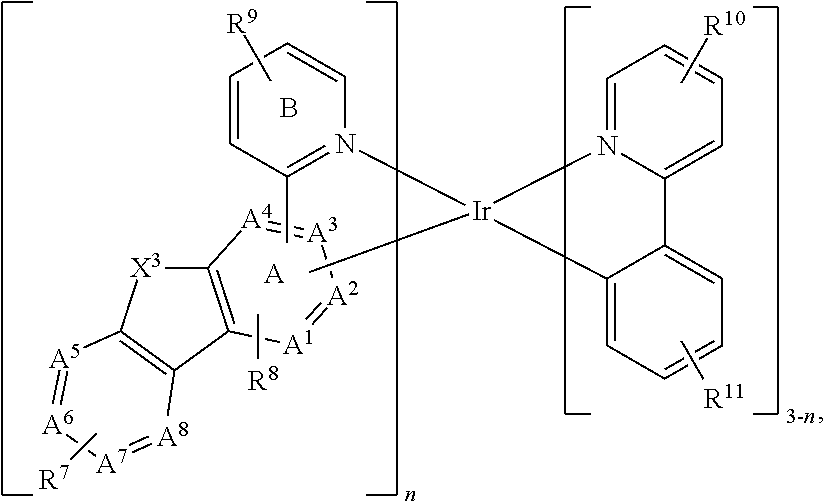


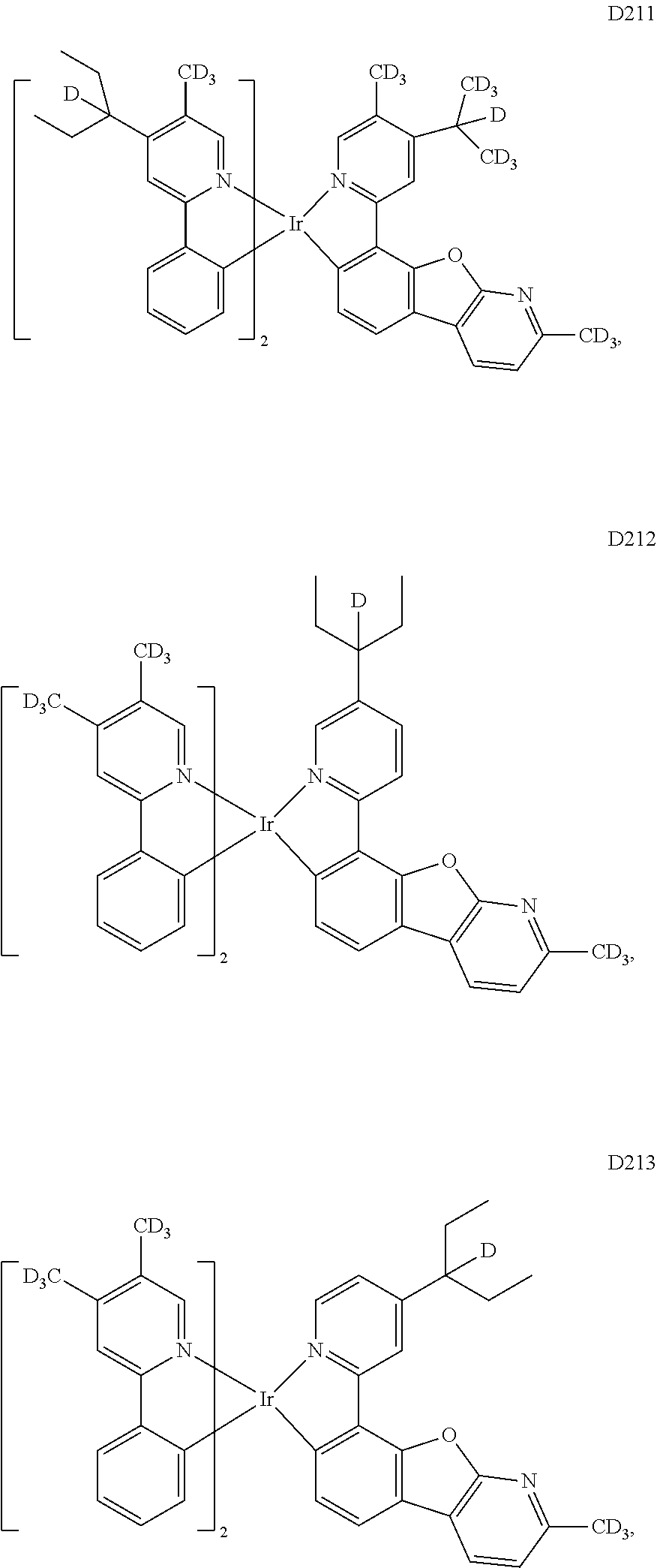


Priority Applications (1)
| Application Number | Priority Date | Filing Date | Title |
|---|---|---|---|
| US15/239,877 US11302872B2 (en) | 2015-09-09 | 2016-08-18 | Organic electroluminescent materials and devices |
Applications Claiming Priority (3)
| Application Number | Priority Date | Filing Date | Title |
|---|---|---|---|
| US201562216113P | 2015-09-09 | 2015-09-09 | |
| US201562240256P | 2015-10-12 | 2015-10-12 | |
| US15/239,877 US11302872B2 (en) | 2015-09-09 | 2016-08-18 | Organic electroluminescent materials and devices |
Publications (2)
| Publication Number | Publication Date |
|---|---|
| US20170069848A1 US20170069848A1 (en) | 2017-03-09 |
| US11302872B2 true US11302872B2 (en) | 2022-04-12 |
Family
ID=58189832
Family Applications (1)
| Application Number | Title | Priority Date | Filing Date |
|---|---|---|---|
| US15/239,877 Active 2036-10-28 US11302872B2 (en) | 2015-09-09 | 2016-08-18 | Organic electroluminescent materials and devices |
Country Status (1)
| Country | Link |
|---|---|
| US (1) | US11302872B2 (en) |
Cited By (2)
| Publication number | Priority date | Publication date | Assignee | Title |
|---|---|---|---|---|
| US20210114954A1 (en) * | 2016-11-23 | 2021-04-22 | Guangzhou Chinaray Optoelectronic Materials Ltd. | Fused ring compound, high polymer, mixture, composition and organic electronic component |
| US20220278287A1 (en) * | 2012-11-09 | 2022-09-01 | Universal Display Corporation | Organic electroluminescent materials and devices |
Families Citing this family (51)
| Publication number | Priority date | Publication date | Assignee | Title |
|---|---|---|---|---|
| US10593890B2 (en) | 2015-04-06 | 2020-03-17 | Universal Display Corporation | Organic electroluminescent materials and devices |
| US11818949B2 (en) | 2015-04-06 | 2023-11-14 | Universal Display Corporation | Organic electroluminescent materials and devices |
| US11495749B2 (en) | 2015-04-06 | 2022-11-08 | Universal Display Corporation | Organic electroluminescent materials and devices |
| US10840458B2 (en) | 2016-05-25 | 2020-11-17 | Universal Display Corporation | Organic electroluminescent materials and devices |
| KR102275343B1 (en) * | 2017-02-28 | 2021-07-09 | 삼성에스디아이 주식회사 | Composition for organic optoelectric device and organic optoelectric device and display device |
| US11056658B2 (en) | 2017-03-29 | 2021-07-06 | Universal Display Corporation | Organic electroluminescent materials and devices |
| US10844085B2 (en) | 2017-03-29 | 2020-11-24 | Universal Display Corporation | Organic electroluminescent materials and devices |
| JPWO2018180465A1 (en) * | 2017-03-30 | 2020-03-19 | 日鉄ケミカル&マテリアル株式会社 | Organic electroluminescent device material and organic electroluminescent device |
| CN106977514A (en) * | 2017-03-30 | 2017-07-25 | 上海道亦化工科技有限公司 | A kind of organic electroluminescent compounds and its luminescent device containing carbazole derivates |
| WO2018198844A1 (en) * | 2017-04-27 | 2018-11-01 | 新日鉄住金化学株式会社 | Organic electroluminescent element |
| KR20180137772A (en) * | 2017-06-19 | 2018-12-28 | 삼성에스디아이 주식회사 | Organic optoelectric device and display device |
| KR102008897B1 (en) | 2017-06-22 | 2019-10-23 | 삼성에스디아이 주식회사 | Organic optoelectronic device and display device |
| US20190198772A1 (en) | 2017-06-22 | 2019-06-27 | Samsung Sdi Co., Ltd. | Compound for organic optoelectronic device, composition for organic optoelectronic device and organic optoelectronic device and display deivce |
| KR101947747B1 (en) | 2018-05-04 | 2019-02-13 | 삼성에스디아이 주식회사 | Compound for organic optoelectronic device, composition for organic optoelectronic device and organic optoelectronic device and display device |
| US10968226B2 (en) | 2017-06-23 | 2021-04-06 | Universal Display Corporation | Organic electroluminescent materials and devices |
| KR102162402B1 (en) * | 2017-07-21 | 2020-10-06 | 삼성에스디아이 주식회사 | Organic optoelectronic device and display device |
| US11723269B2 (en) | 2017-08-22 | 2023-08-08 | Universal Display Corporation | Organic electroluminescent materials and devices |
| KR102085165B1 (en) * | 2017-11-10 | 2020-03-05 | 주식회사 엘지화학 | Organic metal compound and organic light emitting device comprising the same |
| US11349081B2 (en) | 2017-11-14 | 2022-05-31 | Beijing Summer Sprout Technology Co., Ltd. | Azaindolocarbazole compounds |
| KR102455286B1 (en) * | 2017-11-17 | 2022-10-18 | 덕산네오룩스 주식회사 | Organic electronic element comprising compound for organic electronic element and electronic device thereof |
| CN109836426A (en) * | 2017-11-28 | 2019-06-04 | 昆山国显光电有限公司 | The organic electroluminescence device of its preparation of 1,3,5- pyrrolotriazine derivatives and application |
| CN109928974A (en) * | 2017-12-15 | 2019-06-25 | 北京鼎材科技有限公司 | Organic compound and its application in organic electroluminescence device |
| WO2019135633A1 (en) | 2018-01-04 | 2019-07-11 | 주식회사 엘지화학 | Novel compound and organic light-emitting device comprising same |
| US20190225635A1 (en) * | 2018-01-19 | 2019-07-25 | Chuanjun Xia | Metal complexes containing substituted pyridine ligands |
| CN108164564A (en) * | 2018-02-09 | 2018-06-15 | 石家庄诚志永华显示材料有限公司 | A kind of metal iridium complex and the organic electroluminescence device comprising the metal iridium complex |
| KR20190098676A (en) * | 2018-02-13 | 2019-08-22 | 삼성디스플레이 주식회사 | Organic light emitting device and display apparatus comprising the same |
| US11217757B2 (en) * | 2018-03-12 | 2022-01-04 | Universal Display Corporation | Host materials for electroluminescent devices |
| KR102186095B1 (en) * | 2018-05-14 | 2020-12-03 | 주식회사 엘지화학 | Compound and organic light emitting device comprising the same |
| WO2019221484A1 (en) * | 2018-05-14 | 2019-11-21 | 주식회사 엘지화학 | Organometallic compound and organic light emitting diode comprising same |
| CN111683955B (en) * | 2018-05-14 | 2023-12-08 | 株式会社Lg化学 | Compound and organic light-emitting element comprising same |
| US11834459B2 (en) | 2018-12-12 | 2023-12-05 | Universal Display Corporation | Host materials for electroluminescent devices |
| KR102471152B1 (en) * | 2019-01-10 | 2022-11-24 | 삼성에스디아이 주식회사 | Compound for organic optoelectronic device, composition for organic optoelectronic device and organic optoelectronic device and display device |
| KR20210050014A (en) | 2019-10-24 | 2021-05-07 | 삼성디스플레이 주식회사 | Organic electroluminescence device and compound for organic electroluminescence device |
| KR20210082311A (en) | 2019-12-24 | 2021-07-05 | 삼성디스플레이 주식회사 | Organic electroluminescence device and polycyclic compound for organic electroluminescence device |
| CN111063818A (en) * | 2019-12-26 | 2020-04-24 | 武汉华星光电半导体显示技术有限公司 | Display panel and preparation method thereof |
| CN114830367A (en) * | 2019-12-27 | 2022-07-29 | 日铁化学材料株式会社 | Organic electroluminescent element and method for manufacturing the same |
| CN113121608B (en) * | 2019-12-31 | 2023-07-04 | 马鞍山南大高新技术研究院有限公司 | Iridium complex with main ligand containing dibenzoheterocycle or aza-dibenzoheterocycle and application thereof |
| CN113121606A (en) * | 2019-12-31 | 2021-07-16 | 马鞍山南大高新技术研究院有限公司 | Iridium complex with picolinic acid as auxiliary ligand and application thereof |
| KR102377021B1 (en) * | 2020-03-06 | 2022-03-21 | 한국생산기술연구원 | Compound for organic electronic element having benzocyclobutene functional group for cross-linked bond, organic electronic element using the same, and an electronic device thereof |
| KR20220161305A (en) * | 2020-03-31 | 2022-12-06 | 닛테츠 케미컬 앤드 머티리얼 가부시키가이샤 | organic electroluminescent device |
| CN111995999B (en) * | 2020-05-06 | 2022-06-24 | 浙江华显光电科技有限公司 | Combination of deuterated guest compound and host compound and photoelectric device comprising same |
| EP3975280A1 (en) * | 2020-09-29 | 2022-03-30 | NIPPON STEEL Chemical & Material Co., Ltd. | Composition for organic electroluminescent element and organic electroluminescent element |
| WO2022124366A1 (en) | 2020-12-11 | 2022-06-16 | 日鉄ケミカル&マテリアル株式会社 | Organic electroluminescent element |
| KR20230119634A (en) | 2020-12-11 | 2023-08-16 | 닛테츠 케미컬 앤드 머티리얼 가부시키가이샤 | Materials for organic electroluminescent devices and organic electroluminescent devices |
| JPWO2022124365A1 (en) | 2020-12-11 | 2022-06-16 | ||
| KR20230121083A (en) | 2020-12-18 | 2023-08-17 | 닛테츠 케미컬 앤드 머티리얼 가부시키가이샤 | Organic electroluminescent device and manufacturing method thereof |
| WO2022149493A1 (en) | 2021-01-08 | 2022-07-14 | 日鉄ケミカル&マテリアル株式会社 | Organic electroluminescent element and method for producing same |
| CN117321034A (en) | 2021-05-31 | 2023-12-29 | 日铁化学材料株式会社 | Deuterated compound and organic electroluminescent element |
| CN117295715A (en) | 2021-05-31 | 2023-12-26 | 日铁化学材料株式会社 | Deuterated compound and organic electroluminescent element |
| KR20240016255A (en) | 2021-05-31 | 2024-02-06 | 닛테츠 케미컬 앤드 머티리얼 가부시키가이샤 | Deuteride and organic electroluminescent devices |
| EP4328285A1 (en) * | 2022-08-25 | 2024-02-28 | Beijing Summer Sprout Technology Co., Ltd. | Organic electroluminescent material and device thereof |
Citations (133)
| Publication number | Priority date | Publication date | Assignee | Title |
|---|---|---|---|---|
| US4769292A (en) | 1987-03-02 | 1988-09-06 | Eastman Kodak Company | Electroluminescent device with modified thin film luminescent zone |
| US5061569A (en) | 1990-07-26 | 1991-10-29 | Eastman Kodak Company | Electroluminescent device with organic electroluminescent medium |
| US5247190A (en) | 1989-04-20 | 1993-09-21 | Cambridge Research And Innovation Limited | Electroluminescent devices |
| EP0650955A1 (en) | 1993-11-01 | 1995-05-03 | Hodogaya Chemical Co., Ltd. | Amine compound and electro-luminescence device comprising same |
| US5703436A (en) | 1994-12-13 | 1997-12-30 | The Trustees Of Princeton University | Transparent contacts for organic devices |
| US5707745A (en) | 1994-12-13 | 1998-01-13 | The Trustees Of Princeton University | Multicolor organic light emitting devices |
| US5834893A (en) | 1996-12-23 | 1998-11-10 | The Trustees Of Princeton University | High efficiency organic light emitting devices with light directing structures |
| US5844363A (en) | 1997-01-23 | 1998-12-01 | The Trustees Of Princeton Univ. | Vacuum deposited, non-polymeric flexible organic light emitting devices |
| US6013982A (en) | 1996-12-23 | 2000-01-11 | The Trustees Of Princeton University | Multicolor display devices |
| US6087196A (en) | 1998-01-30 | 2000-07-11 | The Trustees Of Princeton University | Fabrication of organic semiconductor devices using ink jet printing |
| US6091195A (en) | 1997-02-03 | 2000-07-18 | The Trustees Of Princeton University | Displays having mesa pixel configuration |
| US6097147A (en) | 1998-09-14 | 2000-08-01 | The Trustees Of Princeton University | Structure for high efficiency electroluminescent device |
| WO2001039234A2 (en) | 1999-11-24 | 2001-05-31 | The Trustees Of Princeton University | Organic light emitting diode having a blue phosphorescent molecule as an emitter |
| US6294398B1 (en) | 1999-11-23 | 2001-09-25 | The Trustees Of Princeton University | Method for patterning devices |
| US6303238B1 (en) | 1997-12-01 | 2001-10-16 | The Trustees Of Princeton University | OLEDs doped with phosphorescent compounds |
| US6337102B1 (en) | 1997-11-17 | 2002-01-08 | The Trustees Of Princeton University | Low pressure vapor phase deposition of organic thin films |
| WO2002002714A2 (en) | 2000-06-30 | 2002-01-10 | E.I. Du Pont De Nemours And Company | Electroluminescent iridium compounds with fluorinated phenylpyridines, phenylpyrimidines, and phenylquinolines and devices made with such compounds |
| WO2002015654A1 (en) | 2000-08-04 | 2002-02-21 | Toray Engineering Co., Ltd. | Mounting method and mounting device |
| US20020034656A1 (en) | 1998-09-14 | 2002-03-21 | Thompson Mark E. | Organometallic complexes as phosphorescent emitters in organic LEDs |
| US20020134984A1 (en) | 2001-02-01 | 2002-09-26 | Fuji Photo Film Co., Ltd. | Transition metal complex and light-emitting device |
| US20020158242A1 (en) | 1999-12-31 | 2002-10-31 | Se-Hwan Son | Electronic device comprising organic compound having p-type semiconducting characteristics |
| US6528187B1 (en) | 1998-09-08 | 2003-03-04 | Fuji Photo Film Co., Ltd. | Material for luminescence element and luminescence element using the same |
| WO2003040257A1 (en) | 2001-11-07 | 2003-05-15 | E. I. Du Pont De Nemours And Company | Electroluminescent platinum compounds and devices made with such compounds |
| US20030138657A1 (en) | 2000-12-07 | 2003-07-24 | Canon Kabushiki Kaisha | Deuterated semi-conducting organic compounds used for opto-electronic devices |
| WO2003060956A2 (en) | 2002-01-18 | 2003-07-24 | Lg Chem, Ltd. | New material for transporting electrons and organic electroluminescent display using the same |
| US20030152802A1 (en) | 2001-06-19 | 2003-08-14 | Akira Tsuboyama | Metal coordination compound and organic liminescence device |
| US20030162053A1 (en) | 1996-06-25 | 2003-08-28 | Marks Tobin J. | Organic light - emitting diodes and methods for assembly and enhanced charge injection |
| US20030175553A1 (en) | 2001-12-28 | 2003-09-18 | Thompson Mark E. | White light emitting oleds from combined monomer and aggregate emission |
| US20030230980A1 (en) | 2002-06-18 | 2003-12-18 | Forrest Stephen R | Very low voltage, high efficiency phosphorescent oled in a p-i-n structure |
| US20040016907A1 (en) * | 2000-05-19 | 2004-01-29 | Eastman Kodak Company | Method of using predoped materials for making an organic light-emitting device |
| US6687266B1 (en) | 2002-11-08 | 2004-02-03 | Universal Display Corporation | Organic light emitting materials and devices |
| US20040036077A1 (en) | 2002-08-22 | 2004-02-26 | Fuji Photo Film Co., Ltd. | Light emitting element |
| US20040137268A1 (en) | 2002-12-27 | 2004-07-15 | Fuji Photo Film Co., Ltd. | Organic electroluminescent device |
| US20040137267A1 (en) | 2002-12-27 | 2004-07-15 | Fuji Photo Film Co., Ltd. | Organic electroluminescent device |
| US20040174116A1 (en) | 2001-08-20 | 2004-09-09 | Lu Min-Hao Michael | Transparent electrodes |
| WO2004093207A2 (en) | 2003-04-15 | 2004-10-28 | Covion Organic Semiconductors Gmbh | Mixtures of matrix materials and organic semiconductors capable of emission, use of the same and electronic components containing said mixtures |
| WO2004107822A1 (en) | 2003-05-29 | 2004-12-09 | Nippon Steel Chemical Co., Ltd. | Organic electroluminescent element |
| US6835469B2 (en) | 2001-10-17 | 2004-12-28 | The University Of Southern California | Phosphorescent compounds and devices comprising the same |
| JP2005011610A (en) | 2003-06-18 | 2005-01-13 | Nippon Steel Chem Co Ltd | Organic electroluminescent element |
| US20050025993A1 (en) | 2003-07-25 | 2005-02-03 | Thompson Mark E. | Materials and structures for enhancing the performance of organic light emitting devices |
| WO2005014551A1 (en) | 2003-08-07 | 2005-02-17 | Nippon Steel Chemical Co., Ltd. | Aluminum chelate compelx for organic el material |
| WO2005019373A2 (en) | 2003-08-19 | 2005-03-03 | Basf Aktiengesellschaft | Transition metal complexes comprising carbene ligands serving as emitters for organic light-emitting diodes (oled's) |
| WO2005030900A1 (en) | 2003-09-25 | 2005-04-07 | Nippon Steel Chemical Co., Ltd. | Organic electroluminescent device |
| US20050112407A1 (en) | 2003-11-21 | 2005-05-26 | Fuji Photo Film Co., Ltd. | Organic electroluminescent device |
| US6921915B2 (en) | 2001-03-08 | 2005-07-26 | Canon Kabushiki Kaisha | Metal coordination compound, luminescence device and display apparatus |
| WO2005089025A1 (en) | 2004-03-15 | 2005-09-22 | Nippon Steel Chemical Co., Ltd. | Organic electroluminescent device |
| US20050238919A1 (en) | 2004-04-23 | 2005-10-27 | Fuji Photo Film Co., Ltd. | Organic electroluminescent device |
| US20050244673A1 (en) | 2002-08-27 | 2005-11-03 | Fujitsu Limited | Organometallic complex, organic EL element and organic EL display |
| US20050260449A1 (en) | 2004-05-18 | 2005-11-24 | Robert Walters | Complexes with tridentate ligands |
| US20050260441A1 (en) | 2004-05-18 | 2005-11-24 | Thompson Mark E | Luminescent compounds with carbene ligands |
| WO2005123873A1 (en) | 2004-06-17 | 2005-12-29 | Konica Minolta Holdings, Inc. | Organic electroluminescent device material, organic electroluminescent device, display and illuminating device |
| US20060008670A1 (en) | 2004-07-06 | 2006-01-12 | Chun Lin | Organic light emitting materials and devices |
| WO2006009024A1 (en) | 2004-07-23 | 2006-01-26 | Konica Minolta Holdings, Inc. | Organic electroluminescent device, display and illuminating device |
| WO2006056418A2 (en) | 2004-11-25 | 2006-06-01 | Basf Aktiengesellschaft | Use of transition metal carbene complexes in organic light-emitting diodes (oleds) |
| WO2006072092A1 (en) | 2004-12-29 | 2006-07-06 | Fruitman Clinton O | Transcutaneous electrical nerve stimulator with hot or cold thermal application |
| US7087321B2 (en) | 2003-04-22 | 2006-08-08 | Universal Display Corporation | Organic light emitting devices having reduced pixel shrinkage |
| WO2006082742A1 (en) | 2005-02-04 | 2006-08-10 | Konica Minolta Holdings, Inc. | Organic electroluminescent device material, organic electroluminescent device, display and illuminating device |
| US7090928B2 (en) | 2003-04-01 | 2006-08-15 | The University Of Southern California | Binuclear compounds |
| US20060202194A1 (en) | 2005-03-08 | 2006-09-14 | Jeong Hyun C | Red phosphorescene compounds and organic electroluminescence device using the same |
| WO2006098120A1 (en) | 2005-03-16 | 2006-09-21 | Konica Minolta Holdings, Inc. | Organic electroluminescent device material and organic electroluminescent device |
| WO2006100298A1 (en) | 2005-03-24 | 2006-09-28 | Basf Aktiengesellschaft | Use of compounds containing aromatic or heteroaromatic rings linked via carbonyl group-containing groups, for use as matrix materials in organic light-emitting diodes |
| WO2006103874A1 (en) | 2005-03-29 | 2006-10-05 | Konica Minolta Holdings, Inc. | Organic electroluminescent device material, organic electroluminescent device, display and illuminating device |
| US20060240279A1 (en) | 2005-04-21 | 2006-10-26 | Vadim Adamovich | Non-blocked phosphorescent OLEDs |
| WO2006114966A1 (en) | 2005-04-18 | 2006-11-02 | Konica Minolta Holdings, Inc. | Organic electroluminescent device, display and illuminating device |
| US20060251923A1 (en) | 2005-05-06 | 2006-11-09 | Chun Lin | Stability OLED materials and devices |
| EP1725079A1 (en) | 2004-03-11 | 2006-11-22 | Mitsubishi Chemical Corporation | Composition for charge-transporting film and ion compound, charge-transporting film and organic electroluminescent device using same, and method for manufacturing organic electroluminescent device and method for producing charge-transporting film |
| US20060263635A1 (en) | 2005-05-06 | 2006-11-23 | Fuji Photo Film Co., Ltd. | Organic electroluminescent device |
| WO2006132173A1 (en) | 2005-06-07 | 2006-12-14 | Nippon Steel Chemical Co., Ltd. | Organic metal complex and organic electroluminescent device using same |
| US20060280965A1 (en) | 2005-05-31 | 2006-12-14 | Raymond Kwong | Triphenylene hosts in phosphorescent light emitting diodes |
| US7154114B2 (en) | 2004-05-18 | 2006-12-26 | Universal Display Corporation | Cyclometallated iridium carbene complexes for use as hosts |
| WO2007002683A2 (en) | 2005-06-27 | 2007-01-04 | E. I. Du Pont De Nemours And Company | Electrically conductive polymer compositions |
| WO2007004380A1 (en) | 2005-07-01 | 2007-01-11 | Konica Minolta Holdings, Inc. | Organic electroluminescent element material, organic electroluminescent element, display device, and lighting equipment |
| JP2007123392A (en) | 2005-10-26 | 2007-05-17 | Konica Minolta Holdings Inc | Organic electroluminescence device, display device and lighting device |
| WO2007063754A1 (en) | 2005-12-01 | 2007-06-07 | Nippon Steel Chemical Co., Ltd. | Compound for organic electroluminescent element and organic electroluminescent element |
| WO2007063796A1 (en) | 2005-12-01 | 2007-06-07 | Nippon Steel Chemical Co., Ltd. | Organic electroluminescent device |
| US7250226B2 (en) | 2001-08-31 | 2007-07-31 | Nippon Hoso Kyokai | Phosphorescent compound, a phosphorescent composition and an organic light-emitting device |
| US20070190359A1 (en) | 2006-02-10 | 2007-08-16 | Knowles David B | Metal complexes of cyclometallated imidazo[1,2-ƒ]phenanthridine and diimidazo[1,2-a:1',2'-c]quinazoline ligands and isoelectronic and benzannulated analogs thereof |
| JP2007254297A (en) | 2006-03-20 | 2007-10-04 | Nippon Steel Chem Co Ltd | Compound of light-emitting layer and organic electroluminescent device |
| US20070278938A1 (en) | 2006-04-26 | 2007-12-06 | Idemitsu Kosan Co., Ltd. | Aromatic amine derivative and electroluminescence device using the same |
| US20080015355A1 (en) | 2004-06-28 | 2008-01-17 | Thomas Schafer | Electroluminescent Metal Complexes With Triazoles And Benzotriazoles |
| US7332232B2 (en) | 2004-02-03 | 2008-02-19 | Universal Display Corporation | OLEDs utilizing multidentate ligand systems |
| US7338722B2 (en) | 2003-03-24 | 2008-03-04 | The University Of Southern California | Phenyl and fluorenyl substituted phenyl-pyrazole complexes of Ir |
| JP2008074939A (en) | 2006-09-21 | 2008-04-03 | Konica Minolta Holdings Inc | Organic electroluminescence element material, organic electroluminescence element, display device and illumination device |
| US20080106190A1 (en) | 2006-08-23 | 2008-05-08 | Idemitsu Kosan Co., Ltd. | Aromatic amine derivatives and organic electroluminescent device using same |
| WO2008056746A1 (en) | 2006-11-09 | 2008-05-15 | Nippon Steel Chemical Co., Ltd. | Compound for organic electroluminescent device and organic electroluminescent device |
| US20080124572A1 (en) | 2006-11-24 | 2008-05-29 | Idemitsu Kosan Co., Ltd. | Aromatic amine derivative and organic electroluminescence device using the same |
| US7393599B2 (en) | 2004-05-18 | 2008-07-01 | The University Of Southern California | Luminescent compounds with carbene ligands |
| US7396598B2 (en) | 2001-06-20 | 2008-07-08 | Showa Denko K.K. | Light emitting material and organic light-emitting device |
| WO2008101842A1 (en) | 2007-02-23 | 2008-08-28 | Basf Se | Electroluminescent metal complexes with benzotriazoles |
| US20080220265A1 (en) | 2006-12-08 | 2008-09-11 | Universal Display Corporation | Cross-linkable Iridium Complexes and Organic Light-Emitting Devices Using the Same |
| US7431968B1 (en) | 2001-09-04 | 2008-10-07 | The Trustees Of Princeton University | Process and apparatus for organic vapor jet deposition |
| US7445855B2 (en) | 2004-05-18 | 2008-11-04 | The University Of Southern California | Cationic metal-carbene complexes |
| WO2008132085A1 (en) | 2007-04-26 | 2008-11-06 | Basf Se | Silanes containing phenothiazine-s-oxide or phenothiazine-s,s-dioxide groups and the use thereof in oleds |
| US20080297033A1 (en) | 2006-02-10 | 2008-12-04 | Knowles David B | Blue phosphorescent imidazophenanthridine materials |
| WO2009000673A2 (en) | 2007-06-22 | 2008-12-31 | Basf Se | Light emitting cu(i) complexes |
| WO2009003898A1 (en) | 2007-07-05 | 2009-01-08 | Basf Se | Organic light-emitting diodes containing carbene transition metal complex emitters and at least one compound selected from disilylcarbazoles, disilyldibenzofurans, disilyldibenzothiophenes, disilyldibenzophospholes, disilyldibenzothiophene s-oxides and disilyldibenzothiophene s,s-dioxides |
| US20090008605A1 (en) | 2007-07-07 | 2009-01-08 | Idemitsu Kosan Co., Ltd. | Naphthalene derivative, material for organic electroluminescence device, and organic electroluminescence device using the same |
| US20090009065A1 (en) | 2007-07-07 | 2009-01-08 | Idemitsu Kosan Co., Ltd. | Organic electroluminescence device and material for organic electroluminescence device |
| US20090017330A1 (en) | 2007-07-10 | 2009-01-15 | Idemitsu Kosan Co., Ltd. | Material for organic electroluminescence device and organic electroluminescence device utilizing the same |
| WO2009008311A1 (en) | 2007-07-07 | 2009-01-15 | Idemitsu Kosan Co., Ltd. | Chrysene derivative and organic electroluminescent device using the same |
| US20090030202A1 (en) | 2007-07-10 | 2009-01-29 | Idemitsu Kosan Co., Ltd. | Material for organic electroluminescent element and organic electroluminescent element employing the same |
| WO2009018009A1 (en) | 2007-07-27 | 2009-02-05 | E. I. Du Pont De Nemours And Company | Aqueous dispersions of electrically conducting polymers containing inorganic nanoparticles |
| WO2009021126A2 (en) | 2007-08-08 | 2009-02-12 | Universal Display Corporation | Benzo-fused thiophene or benzo-fused furan compounds comprising a triphenylene group |
| US20090039776A1 (en) | 2007-08-09 | 2009-02-12 | Canon Kabushiki Kaisha | Organometallic complex and organic light-emitting element using same |
| US20090045730A1 (en) | 2007-07-07 | 2009-02-19 | Idemitsu Kosan Co., Ltd. | Organic electroluminescence device and material for organic electroluminescence device |
| US20090045731A1 (en) | 2007-07-07 | 2009-02-19 | Idemitsu Kosan Co., Ltd. | Organic electroluminescence device and material for organic electroluminescence device |
| EP2034538A1 (en) | 2006-06-02 | 2009-03-11 | Idemitsu Kosan Co., Ltd. | Material for organic electroluminescence element, and organic electroluminescence element using the material |
| WO2009050290A1 (en) | 2007-10-17 | 2009-04-23 | Basf Se | Transition metal complexes having bridged carbene ligands and the use thereof in oleds |
| US20090101870A1 (en) | 2007-10-22 | 2009-04-23 | E. I. Du Pont De Nemours And Company | Electron transport bi-layers and devices made with such bi-layers |
| US20090108737A1 (en) | 2006-12-08 | 2009-04-30 | Raymond Kwong | Light-emitting organometallic complexes |
| US20090115316A1 (en) | 2007-11-02 | 2009-05-07 | Shiying Zheng | Organic electroluminescent device having an azatriphenylene derivative |
| US7534505B2 (en) | 2004-05-18 | 2009-05-19 | The University Of Southern California | Organometallic compounds for use in electroluminescent devices |
| WO2009063833A1 (en) | 2007-11-15 | 2009-05-22 | Idemitsu Kosan Co., Ltd. | Benzochrysene derivative and organic electroluminescent device using the same |
| WO2009062578A1 (en) | 2007-11-12 | 2009-05-22 | Merck Patent Gmbh | Organic electroluminescent devices comprising azomethine-metal complexes |
| WO2009066779A1 (en) | 2007-11-22 | 2009-05-28 | Idemitsu Kosan Co., Ltd. | Organic el element |
| WO2009066778A1 (en) | 2007-11-22 | 2009-05-28 | Idemitsu Kosan Co., Ltd. | Organic el element and solution containing organic el material |
| US20090167162A1 (en) | 2007-12-28 | 2009-07-02 | Universal Display Corporation | Dibenzothiophene-containing materials in phosphorescent light emitting diodes |
| US20090165846A1 (en) | 2005-09-07 | 2009-07-02 | Universitaet Braunschweig | Triplet emitter having condensed five-membered rings |
| WO2009086028A2 (en) | 2007-12-28 | 2009-07-09 | Universal Display Corporation | Carbazole-containing materials in phosphorescent light emitting diodes |
| US20090179554A1 (en) | 2006-05-11 | 2009-07-16 | Hitoshi Kuma | Organic electroluminescent device |
| WO2009100991A1 (en) | 2008-02-12 | 2009-08-20 | Basf Se | Electroluminescent metal complexes with dibenzo[f,h]quinoxalines |
| US20100244004A1 (en) * | 2009-03-23 | 2010-09-30 | Universal Display Corporation | Heteroleptic iridium complex |
| WO2011136755A1 (en) | 2010-04-28 | 2011-11-03 | Universal Display Corporation | Depositing premixed materials |
| US20120068170A1 (en) * | 2009-05-29 | 2012-03-22 | Merck Patent Gmbh | Materials for organic electroluminescent devices |
| JP2012140365A (en) * | 2010-12-28 | 2012-07-26 | Idemitsu Kosan Co Ltd | Condensed polycyclic compound, material for organic electroluminescent element, and organic electroluminescent element using the material |
| WO2013056776A1 (en) * | 2011-10-20 | 2013-04-25 | Merck Patent Gmbh | Materials for organic electroluminescent devices |
| WO2013108997A1 (en) * | 2012-01-18 | 2013-07-25 | 덕산하이메탈(주) | Compound for organic electronic device, and organic electronic device and electronic apparatus comprising same |
| US20140054564A1 (en) * | 2010-07-30 | 2014-02-27 | Rohm And Haas Electronic Materials Korea Ltd. | Electroluminescent device using electroluminescent compound as luminescent material |
| US20140061609A1 (en) * | 2010-10-13 | 2014-03-06 | Nam Kyun Kim | Novel compounds for organic electronic material and organic electroluminescent device using the same |
| US20140131676A1 (en) * | 2012-11-09 | 2014-05-15 | Universal Display Corporation | Iridium complexes with aza-benzo fused ligands |
| US20140332793A1 (en) * | 2012-01-18 | 2014-11-13 | Duksan High Metal Co., Ltd. | Compound for organic electric element, organic electric element comprising the same and electronic device thereof |
| US20140364625A1 (en) * | 2012-01-16 | 2014-12-11 | Rohm And Haas Electronic Materials Korea Ltd. | Novel organic electroluminescent compounds and organic electroluminescent device using the same |
| US20150115205A1 (en) | 2012-05-02 | 2015-04-30 | Rohm And Haas Electronic Materials Korea Ltd. | Novel organic electroluminescence compounds and organic electroluminescence device containing the same |
-
2016
- 2016-08-18 US US15/239,877 patent/US11302872B2/en active Active
Patent Citations (140)
| Publication number | Priority date | Publication date | Assignee | Title |
|---|---|---|---|---|
| US4769292A (en) | 1987-03-02 | 1988-09-06 | Eastman Kodak Company | Electroluminescent device with modified thin film luminescent zone |
| US5247190A (en) | 1989-04-20 | 1993-09-21 | Cambridge Research And Innovation Limited | Electroluminescent devices |
| US5061569A (en) | 1990-07-26 | 1991-10-29 | Eastman Kodak Company | Electroluminescent device with organic electroluminescent medium |
| EP0650955A1 (en) | 1993-11-01 | 1995-05-03 | Hodogaya Chemical Co., Ltd. | Amine compound and electro-luminescence device comprising same |
| US5703436A (en) | 1994-12-13 | 1997-12-30 | The Trustees Of Princeton University | Transparent contacts for organic devices |
| US5707745A (en) | 1994-12-13 | 1998-01-13 | The Trustees Of Princeton University | Multicolor organic light emitting devices |
| US20030162053A1 (en) | 1996-06-25 | 2003-08-28 | Marks Tobin J. | Organic light - emitting diodes and methods for assembly and enhanced charge injection |
| US5834893A (en) | 1996-12-23 | 1998-11-10 | The Trustees Of Princeton University | High efficiency organic light emitting devices with light directing structures |
| US6013982A (en) | 1996-12-23 | 2000-01-11 | The Trustees Of Princeton University | Multicolor display devices |
| US5844363A (en) | 1997-01-23 | 1998-12-01 | The Trustees Of Princeton Univ. | Vacuum deposited, non-polymeric flexible organic light emitting devices |
| US6091195A (en) | 1997-02-03 | 2000-07-18 | The Trustees Of Princeton University | Displays having mesa pixel configuration |
| US6337102B1 (en) | 1997-11-17 | 2002-01-08 | The Trustees Of Princeton University | Low pressure vapor phase deposition of organic thin films |
| US6303238B1 (en) | 1997-12-01 | 2001-10-16 | The Trustees Of Princeton University | OLEDs doped with phosphorescent compounds |
| US6087196A (en) | 1998-01-30 | 2000-07-11 | The Trustees Of Princeton University | Fabrication of organic semiconductor devices using ink jet printing |
| US6528187B1 (en) | 1998-09-08 | 2003-03-04 | Fuji Photo Film Co., Ltd. | Material for luminescence element and luminescence element using the same |
| US20020034656A1 (en) | 1998-09-14 | 2002-03-21 | Thompson Mark E. | Organometallic complexes as phosphorescent emitters in organic LEDs |
| US6097147A (en) | 1998-09-14 | 2000-08-01 | The Trustees Of Princeton University | Structure for high efficiency electroluminescent device |
| US6294398B1 (en) | 1999-11-23 | 2001-09-25 | The Trustees Of Princeton University | Method for patterning devices |
| US6468819B1 (en) | 1999-11-23 | 2002-10-22 | The Trustees Of Princeton University | Method for patterning organic thin film devices using a die |
| WO2001039234A2 (en) | 1999-11-24 | 2001-05-31 | The Trustees Of Princeton University | Organic light emitting diode having a blue phosphorescent molecule as an emitter |
| US20020158242A1 (en) | 1999-12-31 | 2002-10-31 | Se-Hwan Son | Electronic device comprising organic compound having p-type semiconducting characteristics |
| US20040016907A1 (en) * | 2000-05-19 | 2004-01-29 | Eastman Kodak Company | Method of using predoped materials for making an organic light-emitting device |
| WO2002002714A2 (en) | 2000-06-30 | 2002-01-10 | E.I. Du Pont De Nemours And Company | Electroluminescent iridium compounds with fluorinated phenylpyridines, phenylpyrimidines, and phenylquinolines and devices made with such compounds |
| WO2002015654A1 (en) | 2000-08-04 | 2002-02-21 | Toray Engineering Co., Ltd. | Mounting method and mounting device |
| US20030138657A1 (en) | 2000-12-07 | 2003-07-24 | Canon Kabushiki Kaisha | Deuterated semi-conducting organic compounds used for opto-electronic devices |
| US20020134984A1 (en) | 2001-02-01 | 2002-09-26 | Fuji Photo Film Co., Ltd. | Transition metal complex and light-emitting device |
| US6921915B2 (en) | 2001-03-08 | 2005-07-26 | Canon Kabushiki Kaisha | Metal coordination compound, luminescence device and display apparatus |
| US20030152802A1 (en) | 2001-06-19 | 2003-08-14 | Akira Tsuboyama | Metal coordination compound and organic liminescence device |
| US7396598B2 (en) | 2001-06-20 | 2008-07-08 | Showa Denko K.K. | Light emitting material and organic light-emitting device |
| US20040174116A1 (en) | 2001-08-20 | 2004-09-09 | Lu Min-Hao Michael | Transparent electrodes |
| US7250226B2 (en) | 2001-08-31 | 2007-07-31 | Nippon Hoso Kyokai | Phosphorescent compound, a phosphorescent composition and an organic light-emitting device |
| US7431968B1 (en) | 2001-09-04 | 2008-10-07 | The Trustees Of Princeton University | Process and apparatus for organic vapor jet deposition |
| US6835469B2 (en) | 2001-10-17 | 2004-12-28 | The University Of Southern California | Phosphorescent compounds and devices comprising the same |
| WO2003040257A1 (en) | 2001-11-07 | 2003-05-15 | E. I. Du Pont De Nemours And Company | Electroluminescent platinum compounds and devices made with such compounds |
| US20030175553A1 (en) | 2001-12-28 | 2003-09-18 | Thompson Mark E. | White light emitting oleds from combined monomer and aggregate emission |
| WO2003060956A2 (en) | 2002-01-18 | 2003-07-24 | Lg Chem, Ltd. | New material for transporting electrons and organic electroluminescent display using the same |
| US20030230980A1 (en) | 2002-06-18 | 2003-12-18 | Forrest Stephen R | Very low voltage, high efficiency phosphorescent oled in a p-i-n structure |
| US20040036077A1 (en) | 2002-08-22 | 2004-02-26 | Fuji Photo Film Co., Ltd. | Light emitting element |
| US20050244673A1 (en) | 2002-08-27 | 2005-11-03 | Fujitsu Limited | Organometallic complex, organic EL element and organic EL display |
| US6687266B1 (en) | 2002-11-08 | 2004-02-03 | Universal Display Corporation | Organic light emitting materials and devices |
| US20040137268A1 (en) | 2002-12-27 | 2004-07-15 | Fuji Photo Film Co., Ltd. | Organic electroluminescent device |
| US20040137267A1 (en) | 2002-12-27 | 2004-07-15 | Fuji Photo Film Co., Ltd. | Organic electroluminescent device |
| US7338722B2 (en) | 2003-03-24 | 2008-03-04 | The University Of Southern California | Phenyl and fluorenyl substituted phenyl-pyrazole complexes of Ir |
| US7090928B2 (en) | 2003-04-01 | 2006-08-15 | The University Of Southern California | Binuclear compounds |
| WO2004093207A2 (en) | 2003-04-15 | 2004-10-28 | Covion Organic Semiconductors Gmbh | Mixtures of matrix materials and organic semiconductors capable of emission, use of the same and electronic components containing said mixtures |
| US7087321B2 (en) | 2003-04-22 | 2006-08-08 | Universal Display Corporation | Organic light emitting devices having reduced pixel shrinkage |
| WO2004107822A1 (en) | 2003-05-29 | 2004-12-09 | Nippon Steel Chemical Co., Ltd. | Organic electroluminescent element |
| JP2005011610A (en) | 2003-06-18 | 2005-01-13 | Nippon Steel Chem Co Ltd | Organic electroluminescent element |
| US20050025993A1 (en) | 2003-07-25 | 2005-02-03 | Thompson Mark E. | Materials and structures for enhancing the performance of organic light emitting devices |
| WO2005014551A1 (en) | 2003-08-07 | 2005-02-17 | Nippon Steel Chemical Co., Ltd. | Aluminum chelate compelx for organic el material |
| WO2005019373A2 (en) | 2003-08-19 | 2005-03-03 | Basf Aktiengesellschaft | Transition metal complexes comprising carbene ligands serving as emitters for organic light-emitting diodes (oled's) |
| WO2005030900A1 (en) | 2003-09-25 | 2005-04-07 | Nippon Steel Chemical Co., Ltd. | Organic electroluminescent device |
| US20050112407A1 (en) | 2003-11-21 | 2005-05-26 | Fuji Photo Film Co., Ltd. | Organic electroluminescent device |
| US7332232B2 (en) | 2004-02-03 | 2008-02-19 | Universal Display Corporation | OLEDs utilizing multidentate ligand systems |
| EP1725079A1 (en) | 2004-03-11 | 2006-11-22 | Mitsubishi Chemical Corporation | Composition for charge-transporting film and ion compound, charge-transporting film and organic electroluminescent device using same, and method for manufacturing organic electroluminescent device and method for producing charge-transporting film |
| WO2005089025A1 (en) | 2004-03-15 | 2005-09-22 | Nippon Steel Chemical Co., Ltd. | Organic electroluminescent device |
| US20050238919A1 (en) | 2004-04-23 | 2005-10-27 | Fuji Photo Film Co., Ltd. | Organic electroluminescent device |
| US7154114B2 (en) | 2004-05-18 | 2006-12-26 | Universal Display Corporation | Cyclometallated iridium carbene complexes for use as hosts |
| US7534505B2 (en) | 2004-05-18 | 2009-05-19 | The University Of Southern California | Organometallic compounds for use in electroluminescent devices |
| US7279704B2 (en) | 2004-05-18 | 2007-10-09 | The University Of Southern California | Complexes with tridentate ligands |
| US20050260441A1 (en) | 2004-05-18 | 2005-11-24 | Thompson Mark E | Luminescent compounds with carbene ligands |
| US7393599B2 (en) | 2004-05-18 | 2008-07-01 | The University Of Southern California | Luminescent compounds with carbene ligands |
| US7445855B2 (en) | 2004-05-18 | 2008-11-04 | The University Of Southern California | Cationic metal-carbene complexes |
| US20050260449A1 (en) | 2004-05-18 | 2005-11-24 | Robert Walters | Complexes with tridentate ligands |
| WO2005123873A1 (en) | 2004-06-17 | 2005-12-29 | Konica Minolta Holdings, Inc. | Organic electroluminescent device material, organic electroluminescent device, display and illuminating device |
| US20080015355A1 (en) | 2004-06-28 | 2008-01-17 | Thomas Schafer | Electroluminescent Metal Complexes With Triazoles And Benzotriazoles |
| US20060008670A1 (en) | 2004-07-06 | 2006-01-12 | Chun Lin | Organic light emitting materials and devices |
| WO2006009024A1 (en) | 2004-07-23 | 2006-01-26 | Konica Minolta Holdings, Inc. | Organic electroluminescent device, display and illuminating device |
| WO2006056418A2 (en) | 2004-11-25 | 2006-06-01 | Basf Aktiengesellschaft | Use of transition metal carbene complexes in organic light-emitting diodes (oleds) |
| US20080018221A1 (en) | 2004-11-25 | 2008-01-24 | Basf Aktiengesellschaft | Use Of Transition Metal Carbene Complexes In Organic Light-Emitting Diodes (Oleds) |
| WO2006072092A1 (en) | 2004-12-29 | 2006-07-06 | Fruitman Clinton O | Transcutaneous electrical nerve stimulator with hot or cold thermal application |
| WO2006082742A1 (en) | 2005-02-04 | 2006-08-10 | Konica Minolta Holdings, Inc. | Organic electroluminescent device material, organic electroluminescent device, display and illuminating device |
| US20060202194A1 (en) | 2005-03-08 | 2006-09-14 | Jeong Hyun C | Red phosphorescene compounds and organic electroluminescence device using the same |
| WO2006098120A1 (en) | 2005-03-16 | 2006-09-21 | Konica Minolta Holdings, Inc. | Organic electroluminescent device material and organic electroluminescent device |
| WO2006100298A1 (en) | 2005-03-24 | 2006-09-28 | Basf Aktiengesellschaft | Use of compounds containing aromatic or heteroaromatic rings linked via carbonyl group-containing groups, for use as matrix materials in organic light-emitting diodes |
| WO2006103874A1 (en) | 2005-03-29 | 2006-10-05 | Konica Minolta Holdings, Inc. | Organic electroluminescent device material, organic electroluminescent device, display and illuminating device |
| WO2006114966A1 (en) | 2005-04-18 | 2006-11-02 | Konica Minolta Holdings, Inc. | Organic electroluminescent device, display and illuminating device |
| US20060240279A1 (en) | 2005-04-21 | 2006-10-26 | Vadim Adamovich | Non-blocked phosphorescent OLEDs |
| US20060263635A1 (en) | 2005-05-06 | 2006-11-23 | Fuji Photo Film Co., Ltd. | Organic electroluminescent device |
| US20060251923A1 (en) | 2005-05-06 | 2006-11-09 | Chun Lin | Stability OLED materials and devices |
| US20060280965A1 (en) | 2005-05-31 | 2006-12-14 | Raymond Kwong | Triphenylene hosts in phosphorescent light emitting diodes |
| WO2006132173A1 (en) | 2005-06-07 | 2006-12-14 | Nippon Steel Chemical Co., Ltd. | Organic metal complex and organic electroluminescent device using same |
| WO2007002683A2 (en) | 2005-06-27 | 2007-01-04 | E. I. Du Pont De Nemours And Company | Electrically conductive polymer compositions |
| WO2007004380A1 (en) | 2005-07-01 | 2007-01-11 | Konica Minolta Holdings, Inc. | Organic electroluminescent element material, organic electroluminescent element, display device, and lighting equipment |
| US20090165846A1 (en) | 2005-09-07 | 2009-07-02 | Universitaet Braunschweig | Triplet emitter having condensed five-membered rings |
| JP2007123392A (en) | 2005-10-26 | 2007-05-17 | Konica Minolta Holdings Inc | Organic electroluminescence device, display device and lighting device |
| WO2007063796A1 (en) | 2005-12-01 | 2007-06-07 | Nippon Steel Chemical Co., Ltd. | Organic electroluminescent device |
| US20090295276A1 (en) * | 2005-12-01 | 2009-12-03 | Tohru Asari | Organic Electroluminescent Device |
| WO2007063754A1 (en) | 2005-12-01 | 2007-06-07 | Nippon Steel Chemical Co., Ltd. | Compound for organic electroluminescent element and organic electroluminescent element |
| US20070190359A1 (en) | 2006-02-10 | 2007-08-16 | Knowles David B | Metal complexes of cyclometallated imidazo[1,2-ƒ]phenanthridine and diimidazo[1,2-a:1',2'-c]quinazoline ligands and isoelectronic and benzannulated analogs thereof |
| US20080297033A1 (en) | 2006-02-10 | 2008-12-04 | Knowles David B | Blue phosphorescent imidazophenanthridine materials |
| JP2007254297A (en) | 2006-03-20 | 2007-10-04 | Nippon Steel Chem Co Ltd | Compound of light-emitting layer and organic electroluminescent device |
| US20070278938A1 (en) | 2006-04-26 | 2007-12-06 | Idemitsu Kosan Co., Ltd. | Aromatic amine derivative and electroluminescence device using the same |
| US20090179554A1 (en) | 2006-05-11 | 2009-07-16 | Hitoshi Kuma | Organic electroluminescent device |
| EP2034538A1 (en) | 2006-06-02 | 2009-03-11 | Idemitsu Kosan Co., Ltd. | Material for organic electroluminescence element, and organic electroluminescence element using the material |
| US20080106190A1 (en) | 2006-08-23 | 2008-05-08 | Idemitsu Kosan Co., Ltd. | Aromatic amine derivatives and organic electroluminescent device using same |
| JP2008074939A (en) | 2006-09-21 | 2008-04-03 | Konica Minolta Holdings Inc | Organic electroluminescence element material, organic electroluminescence element, display device and illumination device |
| WO2008056746A1 (en) | 2006-11-09 | 2008-05-15 | Nippon Steel Chemical Co., Ltd. | Compound for organic electroluminescent device and organic electroluminescent device |
| US20100187977A1 (en) * | 2006-11-09 | 2010-07-29 | Nippon Steel Chemical Co., Ltd. | Compound for use in organic electroluminescent device and organic electroluminescent device |
| US20080124572A1 (en) | 2006-11-24 | 2008-05-29 | Idemitsu Kosan Co., Ltd. | Aromatic amine derivative and organic electroluminescence device using the same |
| US20080220265A1 (en) | 2006-12-08 | 2008-09-11 | Universal Display Corporation | Cross-linkable Iridium Complexes and Organic Light-Emitting Devices Using the Same |
| US20090108737A1 (en) | 2006-12-08 | 2009-04-30 | Raymond Kwong | Light-emitting organometallic complexes |
| WO2008101842A1 (en) | 2007-02-23 | 2008-08-28 | Basf Se | Electroluminescent metal complexes with benzotriazoles |
| WO2008132085A1 (en) | 2007-04-26 | 2008-11-06 | Basf Se | Silanes containing phenothiazine-s-oxide or phenothiazine-s,s-dioxide groups and the use thereof in oleds |
| WO2009000673A2 (en) | 2007-06-22 | 2008-12-31 | Basf Se | Light emitting cu(i) complexes |
| WO2009003898A1 (en) | 2007-07-05 | 2009-01-08 | Basf Se | Organic light-emitting diodes containing carbene transition metal complex emitters and at least one compound selected from disilylcarbazoles, disilyldibenzofurans, disilyldibenzothiophenes, disilyldibenzophospholes, disilyldibenzothiophene s-oxides and disilyldibenzothiophene s,s-dioxides |
| US20090009065A1 (en) | 2007-07-07 | 2009-01-08 | Idemitsu Kosan Co., Ltd. | Organic electroluminescence device and material for organic electroluminescence device |
| US20090045730A1 (en) | 2007-07-07 | 2009-02-19 | Idemitsu Kosan Co., Ltd. | Organic electroluminescence device and material for organic electroluminescence device |
| US20090045731A1 (en) | 2007-07-07 | 2009-02-19 | Idemitsu Kosan Co., Ltd. | Organic electroluminescence device and material for organic electroluminescence device |
| WO2009008311A1 (en) | 2007-07-07 | 2009-01-15 | Idemitsu Kosan Co., Ltd. | Chrysene derivative and organic electroluminescent device using the same |
| US20090008605A1 (en) | 2007-07-07 | 2009-01-08 | Idemitsu Kosan Co., Ltd. | Naphthalene derivative, material for organic electroluminescence device, and organic electroluminescence device using the same |
| US20090030202A1 (en) | 2007-07-10 | 2009-01-29 | Idemitsu Kosan Co., Ltd. | Material for organic electroluminescent element and organic electroluminescent element employing the same |
| US20090017330A1 (en) | 2007-07-10 | 2009-01-15 | Idemitsu Kosan Co., Ltd. | Material for organic electroluminescence device and organic electroluminescence device utilizing the same |
| WO2009018009A1 (en) | 2007-07-27 | 2009-02-05 | E. I. Du Pont De Nemours And Company | Aqueous dispersions of electrically conducting polymers containing inorganic nanoparticles |
| WO2009021126A2 (en) | 2007-08-08 | 2009-02-12 | Universal Display Corporation | Benzo-fused thiophene or benzo-fused furan compounds comprising a triphenylene group |
| US20090039776A1 (en) | 2007-08-09 | 2009-02-12 | Canon Kabushiki Kaisha | Organometallic complex and organic light-emitting element using same |
| WO2009050290A1 (en) | 2007-10-17 | 2009-04-23 | Basf Se | Transition metal complexes having bridged carbene ligands and the use thereof in oleds |
| US20090101870A1 (en) | 2007-10-22 | 2009-04-23 | E. I. Du Pont De Nemours And Company | Electron transport bi-layers and devices made with such bi-layers |
| US20090115316A1 (en) | 2007-11-02 | 2009-05-07 | Shiying Zheng | Organic electroluminescent device having an azatriphenylene derivative |
| WO2009062578A1 (en) | 2007-11-12 | 2009-05-22 | Merck Patent Gmbh | Organic electroluminescent devices comprising azomethine-metal complexes |
| WO2009063833A1 (en) | 2007-11-15 | 2009-05-22 | Idemitsu Kosan Co., Ltd. | Benzochrysene derivative and organic electroluminescent device using the same |
| WO2009066778A1 (en) | 2007-11-22 | 2009-05-28 | Idemitsu Kosan Co., Ltd. | Organic el element and solution containing organic el material |
| WO2009066779A1 (en) | 2007-11-22 | 2009-05-28 | Idemitsu Kosan Co., Ltd. | Organic el element |
| US20090167162A1 (en) | 2007-12-28 | 2009-07-02 | Universal Display Corporation | Dibenzothiophene-containing materials in phosphorescent light emitting diodes |
| WO2009086028A2 (en) | 2007-12-28 | 2009-07-09 | Universal Display Corporation | Carbazole-containing materials in phosphorescent light emitting diodes |
| WO2009100991A1 (en) | 2008-02-12 | 2009-08-20 | Basf Se | Electroluminescent metal complexes with dibenzo[f,h]quinoxalines |
| US20100244004A1 (en) * | 2009-03-23 | 2010-09-30 | Universal Display Corporation | Heteroleptic iridium complex |
| US20120068170A1 (en) * | 2009-05-29 | 2012-03-22 | Merck Patent Gmbh | Materials for organic electroluminescent devices |
| WO2011136755A1 (en) | 2010-04-28 | 2011-11-03 | Universal Display Corporation | Depositing premixed materials |
| US20130112952A1 (en) * | 2010-04-28 | 2013-05-09 | Nippon Steel Chemical Co., Ltd. | Depositing premixed materials |
| US20140054564A1 (en) * | 2010-07-30 | 2014-02-27 | Rohm And Haas Electronic Materials Korea Ltd. | Electroluminescent device using electroluminescent compound as luminescent material |
| US20140061609A1 (en) * | 2010-10-13 | 2014-03-06 | Nam Kyun Kim | Novel compounds for organic electronic material and organic electroluminescent device using the same |
| JP2012140365A (en) * | 2010-12-28 | 2012-07-26 | Idemitsu Kosan Co Ltd | Condensed polycyclic compound, material for organic electroluminescent element, and organic electroluminescent element using the material |
| WO2013056776A1 (en) * | 2011-10-20 | 2013-04-25 | Merck Patent Gmbh | Materials for organic electroluminescent devices |
| US20140275530A1 (en) * | 2011-10-20 | 2014-09-18 | Merck Patent Gmbh | Materials for organic electroluminescent devices |
| US20140364625A1 (en) * | 2012-01-16 | 2014-12-11 | Rohm And Haas Electronic Materials Korea Ltd. | Novel organic electroluminescent compounds and organic electroluminescent device using the same |
| WO2013108997A1 (en) * | 2012-01-18 | 2013-07-25 | 덕산하이메탈(주) | Compound for organic electronic device, and organic electronic device and electronic apparatus comprising same |
| US20140332793A1 (en) * | 2012-01-18 | 2014-11-13 | Duksan High Metal Co., Ltd. | Compound for organic electric element, organic electric element comprising the same and electronic device thereof |
| US20150115205A1 (en) | 2012-05-02 | 2015-04-30 | Rohm And Haas Electronic Materials Korea Ltd. | Novel organic electroluminescence compounds and organic electroluminescence device containing the same |
| US20140131676A1 (en) * | 2012-11-09 | 2014-05-15 | Universal Display Corporation | Iridium complexes with aza-benzo fused ligands |
Non-Patent Citations (47)
Cited By (3)
| Publication number | Priority date | Publication date | Assignee | Title |
|---|---|---|---|---|
| US20220278287A1 (en) * | 2012-11-09 | 2022-09-01 | Universal Display Corporation | Organic electroluminescent materials and devices |
| US20210114954A1 (en) * | 2016-11-23 | 2021-04-22 | Guangzhou Chinaray Optoelectronic Materials Ltd. | Fused ring compound, high polymer, mixture, composition and organic electronic component |
| US11518723B2 (en) * | 2016-11-23 | 2022-12-06 | Guangzhou Chinaray Optoelectronic Materials Ltd. | Fused ring compound, high polymer, mixture, composition and organic electronic component |
Also Published As
| Publication number | Publication date |
|---|---|
| US20170069848A1 (en) | 2017-03-09 |
Similar Documents
| Publication | Publication Date | Title |
|---|---|---|
| US11302872B2 (en) | Organic electroluminescent materials and devices | |
| US11245080B2 (en) | Organic electroluminescent materials and devices | |
| US20210351362A1 (en) | Organic electroluminescent materials and devices | |
| US20210376256A1 (en) | Organic electroluminescent materials and devices | |
| US10418568B2 (en) | Organic electroluminescent materials and devices | |
| US10593892B2 (en) | Organic electroluminescent materials and devices | |
| US11818949B2 (en) | Organic electroluminescent materials and devices | |
| US10418562B2 (en) | Organic electroluminescent materials and devices | |
| US11018309B2 (en) | Organic electroluminescent materials and devices | |
| US20200203616A1 (en) | Organic Electroluminescent Materials and Devices | |
| US10686143B2 (en) | Organic electroluminescent materials and devices | |
| US10777749B2 (en) | Organic electroluminescent materials and devices | |
| US10529931B2 (en) | Organic Electroluminescent materials and devices | |
| US10135006B2 (en) | Organic electroluminescent materials and devices | |
| US10964893B2 (en) | Organic electroluminescent materials and devices | |
| US20200227643A1 (en) | Organic Electroluminescent Materials and Devices | |
| US11081647B2 (en) | Organic electroluminescent materials and devices | |
| US10957866B2 (en) | Organic electroluminescent materials and devices | |
| US10522769B2 (en) | Organic electroluminescent materials and devices | |
| US10476010B2 (en) | Organic electroluminescent materials and devices | |
| US11239432B2 (en) | Organic electroluminescent materials and devices | |
| US10991895B2 (en) | Organic electroluminescent materials and devices | |
| US20240147842A1 (en) | Organic Electroluminescent Materials and Devices | |
| US20180175308A1 (en) | Organic electroluminescent materials and devices |
Legal Events
| Date | Code | Title | Description |
|---|---|---|---|
| AS | Assignment |
Owner name: UNIVERSAL DISPLAY CORPORATION, NEW JERSEY Free format text: ASSIGNMENT OF ASSIGNORS INTEREST;ASSIGNORS:ZENG, LICHANG;ADAMOVICH, VADIM;DYATKIN, ALEXEY BORISOVICH;AND OTHERS;SIGNING DATES FROM 20160718 TO 20160801;REEL/FRAME:039473/0695 |
|
| STPP | Information on status: patent application and granting procedure in general |
Free format text: NON FINAL ACTION MAILED |
|
| STPP | Information on status: patent application and granting procedure in general |
Free format text: RESPONSE TO NON-FINAL OFFICE ACTION ENTERED AND FORWARDED TO EXAMINER |
|
| STPP | Information on status: patent application and granting procedure in general |
Free format text: FINAL REJECTION MAILED |
|
| STPP | Information on status: patent application and granting procedure in general |
Free format text: DOCKETED NEW CASE - READY FOR EXAMINATION |
|
| STPP | Information on status: patent application and granting procedure in general |
Free format text: FINAL REJECTION MAILED |
|
| STPP | Information on status: patent application and granting procedure in general |
Free format text: DOCKETED NEW CASE - READY FOR EXAMINATION |
|
| STPP | Information on status: patent application and granting procedure in general |
Free format text: NON FINAL ACTION MAILED |
|
| STPP | Information on status: patent application and granting procedure in general |
Free format text: RESPONSE TO NON-FINAL OFFICE ACTION ENTERED AND FORWARDED TO EXAMINER |
|
| STPP | Information on status: patent application and granting procedure in general |
Free format text: NOTICE OF ALLOWANCE MAILED -- APPLICATION RECEIVED IN OFFICE OF PUBLICATIONS |
|
| STPP | Information on status: patent application and granting procedure in general |
Free format text: PUBLICATIONS -- ISSUE FEE PAYMENT VERIFIED |
|
| STCF | Information on status: patent grant |
Free format text: PATENTED CASE |
|
| CC | Certificate of correction |