EP3614486B1 - Radio frequency (rf) conductive medium - Google Patents
Radio frequency (rf) conductive medium Download PDFInfo
- Publication number
- EP3614486B1 EP3614486B1 EP19198693.4A EP19198693A EP3614486B1 EP 3614486 B1 EP3614486 B1 EP 3614486B1 EP 19198693 A EP19198693 A EP 19198693A EP 3614486 B1 EP3614486 B1 EP 3614486B1
- Authority
- EP
- European Patent Office
- Prior art keywords
- conductive
- medium
- frequency
- dielectric
- pathways
- Prior art date
- Legal status (The legal status is an assumption and is not a legal conclusion. Google has not performed a legal analysis and makes no representation as to the accuracy of the status listed.)
- Active
Links
- 230000037361 pathway Effects 0.000 claims description 49
- 239000002086 nanomaterial Substances 0.000 claims description 34
- 239000010410 layer Substances 0.000 claims description 24
- 239000000463 material Substances 0.000 claims description 24
- 239000000725 suspension Substances 0.000 claims description 15
- OKTJSMMVPCPJKN-UHFFFAOYSA-N Carbon Chemical compound [C] OKTJSMMVPCPJKN-UHFFFAOYSA-N 0.000 claims description 13
- 239000011241 protective layer Substances 0.000 claims description 13
- BQCADISMDOOEFD-UHFFFAOYSA-N Silver Chemical compound [Ag] BQCADISMDOOEFD-UHFFFAOYSA-N 0.000 claims description 10
- 239000011248 coating agent Substances 0.000 claims description 10
- 238000000576 coating method Methods 0.000 claims description 10
- 229910052709 silver Inorganic materials 0.000 claims description 9
- 239000004332 silver Substances 0.000 claims description 9
- RYGMFSIKBFXOCR-UHFFFAOYSA-N Copper Chemical compound [Cu] RYGMFSIKBFXOCR-UHFFFAOYSA-N 0.000 claims description 8
- 229910052802 copper Inorganic materials 0.000 claims description 8
- 239000010949 copper Substances 0.000 claims description 8
- 229910052782 aluminium Inorganic materials 0.000 claims description 7
- XAGFODPZIPBFFR-UHFFFAOYSA-N aluminium Chemical compound [Al] XAGFODPZIPBFFR-UHFFFAOYSA-N 0.000 claims description 7
- 229910021389 graphene Inorganic materials 0.000 claims description 7
- 229910052799 carbon Inorganic materials 0.000 claims description 6
- 230000035699 permeability Effects 0.000 claims description 6
- 229920000642 polymer Polymers 0.000 claims description 6
- 239000011152 fibreglass Substances 0.000 claims description 5
- PCHJSUWPFVWCPO-UHFFFAOYSA-N gold Chemical compound [Au] PCHJSUWPFVWCPO-UHFFFAOYSA-N 0.000 claims description 5
- 229910052737 gold Inorganic materials 0.000 claims description 5
- 239000010931 gold Substances 0.000 claims description 5
- 239000011230 binding agent Substances 0.000 claims description 4
- 230000001902 propagating effect Effects 0.000 claims description 4
- 239000004020 conductor Substances 0.000 description 11
- 230000004044 response Effects 0.000 description 11
- 230000002500 effect on skin Effects 0.000 description 10
- 239000002904 solvent Substances 0.000 description 7
- 238000010586 diagram Methods 0.000 description 6
- 238000005516 engineering process Methods 0.000 description 6
- 230000001965 increasing effect Effects 0.000 description 4
- 239000002048 multi walled nanotube Substances 0.000 description 4
- 239000002109 single walled nanotube Substances 0.000 description 4
- 230000008878 coupling Effects 0.000 description 3
- 238000010168 coupling process Methods 0.000 description 3
- 238000005859 coupling reaction Methods 0.000 description 3
- PXHVJJICTQNCMI-UHFFFAOYSA-N Nickel Chemical compound [Ni] PXHVJJICTQNCMI-UHFFFAOYSA-N 0.000 description 2
- 230000005540 biological transmission Effects 0.000 description 2
- 239000000470 constituent Substances 0.000 description 2
- 230000005670 electromagnetic radiation Effects 0.000 description 2
- 230000001939 inductive effect Effects 0.000 description 2
- 238000003780 insertion Methods 0.000 description 2
- 230000037431 insertion Effects 0.000 description 2
- 238000009413 insulation Methods 0.000 description 2
- 230000002452 interceptive effect Effects 0.000 description 2
- 230000007246 mechanism Effects 0.000 description 2
- 238000002044 microwave spectrum Methods 0.000 description 2
- 230000000737 periodic effect Effects 0.000 description 2
- 238000001228 spectrum Methods 0.000 description 2
- 230000035882 stress Effects 0.000 description 2
- 230000008646 thermal stress Effects 0.000 description 2
- 230000015572 biosynthetic process Effects 0.000 description 1
- 239000007767 bonding agent Substances 0.000 description 1
- 239000000919 ceramic Substances 0.000 description 1
- 239000002131 composite material Substances 0.000 description 1
- 230000007423 decrease Effects 0.000 description 1
- 230000001419 dependent effect Effects 0.000 description 1
- 239000003989 dielectric material Substances 0.000 description 1
- 229920001971 elastomer Polymers 0.000 description 1
- 239000000806 elastomer Substances 0.000 description 1
- 230000005672 electromagnetic field Effects 0.000 description 1
- 239000011159 matrix material Substances 0.000 description 1
- 239000000155 melt Substances 0.000 description 1
- 238000002844 melting Methods 0.000 description 1
- 230000008018 melting Effects 0.000 description 1
- 238000000034 method Methods 0.000 description 1
- 239000000203 mixture Substances 0.000 description 1
- 229910052759 nickel Inorganic materials 0.000 description 1
- 230000010355 oscillation Effects 0.000 description 1
- 230000005855 radiation Effects 0.000 description 1
- 238000005245 sintering Methods 0.000 description 1
- 230000000638 stimulation Effects 0.000 description 1
Images


Classifications
-
- H—ELECTRICITY
- H01—ELECTRIC ELEMENTS
- H01P—WAVEGUIDES; RESONATORS, LINES, OR OTHER DEVICES OF THE WAVEGUIDE TYPE
- H01P3/00—Waveguides; Transmission lines of the waveguide type
- H01P3/16—Dielectric waveguides, i.e. without a longitudinal conductor
-
- H—ELECTRICITY
- H01—ELECTRIC ELEMENTS
- H01P—WAVEGUIDES; RESONATORS, LINES, OR OTHER DEVICES OF THE WAVEGUIDE TYPE
- H01P7/00—Resonators of the waveguide type
- H01P7/04—Coaxial resonators
-
- H—ELECTRICITY
- H01—ELECTRIC ELEMENTS
- H01B—CABLES; CONDUCTORS; INSULATORS; SELECTION OF MATERIALS FOR THEIR CONDUCTIVE, INSULATING OR DIELECTRIC PROPERTIES
- H01B1/00—Conductors or conductive bodies characterised by the conductive materials; Selection of materials as conductors
- H01B1/20—Conductive material dispersed in non-conductive organic material
- H01B1/24—Conductive material dispersed in non-conductive organic material the conductive material comprising carbon-silicon compounds, carbon or silicon
-
- H—ELECTRICITY
- H01—ELECTRIC ELEMENTS
- H01P—WAVEGUIDES; RESONATORS, LINES, OR OTHER DEVICES OF THE WAVEGUIDE TYPE
- H01P3/00—Waveguides; Transmission lines of the waveguide type
- H01P3/10—Wire waveguides, i.e. with a single solid longitudinal conductor
-
- H—ELECTRICITY
- H01—ELECTRIC ELEMENTS
- H01P—WAVEGUIDES; RESONATORS, LINES, OR OTHER DEVICES OF THE WAVEGUIDE TYPE
- H01P7/00—Resonators of the waveguide type
- H01P7/06—Cavity resonators
Definitions
- Electromagnetic waves or electromagnetic radiation is a form of energy that has both electric and magnetic field components. Electromagnetic waves can have many different frequencies.
- Modern telecommunication systems manipulate electromagnetic waves in the electromagnetic spectrum in order to provide wireless communications to subscribers of the telecommunication systems.
- modern telecommunication systems manipulate those waves having a frequency categorizing them as Radio Frequency (RF) waves.
- RF waves In order to utilize RF waves, telecommunication systems utilize certain essential hardware components, such as filters, mixers, amplifiers, and antennas.
- the technology described herein relates to a radio frequency (RF) conductive medium for improving the conductive efficiency of an RF device.
- the RF conductive medium improves the conductive efficiency of the RF device by including one or more conductive pathways in a transverse electromagnetic axis that is free from the loss inducing impact of skin effect at the radio frequencies of interest.
- the main embodiment of the invention is defined in claim 1.
- each of the plurality of continuous conductive pathways may be a conductive layer in a plurality of conductive layers of conductive pathways.
- Each of the plurality of conductive layers may be structured and have uniform position or arrangement with respect to other layers of the plurality of conductive layers.
- each of the plurality of conductive layers may be unstructured and have a mesh arrangement with respect to other layers of the plurality of conductive layers.
- the transverse electromagnetic axis is an axis parallel to a surface upon which the RF conductive medium is applied. In other embodiments the transverse electromagnetic axis is an axis that is coplanar to a surface upon which the RF conductive medium is applied.
- the RF conductive medium may also include a solvent configured to maintain the RF conductive medium in a viscous state during application of the RF conductive medium onto a dielectric surface.
- the solvent is configured to evaporate in response to being stimulated by a heat source.
- Each medium of the diversity of conductive media may be made of a nanomaterial composed of an element that is at least one of: silver, copper, aluminum, and gold. Also, each medium of the diversity of conductive media may have a structure that is at least one of: wire, ribbon, tube, and flake.
- each of the plurality of continuous conductive pathways may have a conductive cross-sectional area no greater than skin depth at a desired frequency of operation.
- the desired frequency of operation may correspond to at least one of: a desired resonant frequency of a cavity filter, a desired resonant frequency of an antenna, a cutoff frequency of a waveguide, a desired operational frequency range of a coaxial cable, and combined operational frequency ranges of an integrated structure including a cavity filter and an antenna.
- Each of the plurality of continuous conductive pathways may have a uniform conductive cross-sectional area having a skin depth of 50 nm - 4000 nm. In other examples, each of the plurality of continuous conductive pathways may have a uniform conductive cross-sectional area having a skin depth of 1000 nm - 3000 nm. In yet another example, each of the plurality of continuous conductive pathways may have a uniform conductive cross-sectional area having a skin depth of 1500 nm - 2500 nm.
- the RF conductive medium may also include a protective layer covering the plurality of layers of continuous conductive pathways, where the protective layer includes a material that is non-conductive and minimally absorptive to RF energy at a desired frequency of operation.
- the material may be at least one of: a polymer coating and fiberglass coating.
- the suspension dielectric comprises a layer of RF inert material which is non-conductive and minimally absorptive to RF energy ata desired frequency of operation.
- the layer of RF inert material is configured to secure the diversity of conductive media onto a dielectric surface.
- the RF inert material may be at least one of: a polymer coating and fiberglass coating.
- the RF conductive medium may also include a binding agent to bind the RF conductive medium to the surface.
- the RF conductive medium may further include a solvent configured to maintain the RF conductive medium in a viscous state during application of the RF conductive medium onto the dielectric surface.
- the solvent further is configured to evaporate in response to being stimulated by a heat source.
- Each medium of the diversity of conductive media may be made of a nanomaterial composed of an element that is at least one of: carbon and graphene.
- the dielectric surface may be an inner surface of a cavity having an internal geometry corresponding to a desired frequency response characteristic of the cavity.
- the bundle of discrete nanostructures may be applied to an outer surface of a first dielectric surface and to a concentric inner surface of a second dielectric surface.
- the first dielectric surface is an inner conductor and the second dielectric surface is an outer conductor of a coaxial cable.
- the bundle of discrete conductive nanostructures may be applied to a dielectric structure, where the geometry of the dielectric structure and conductive properties of the bundle of discrete conductive nanostructures define a resonant frequency response and radiation pattern of an antenna.
- Modern telecommunication systems manipulate electromagnetic waves having a range of wavelengths in the electromagnetic spectrum that categorize them as Radio Frequency (RF) waves.
- RF Radio Frequency
- telecommunication systems employ certain essential RF hardware components such as filters, mixers, amplifiers, and antennas.
- the RF hardware components interact with the RF waves via RF conductive elements.
- the RF conductive elements are generally composed of an RF conductive medium, such as, aluminum, copper, silver, and gold.
- RF conductive medium such as, aluminum, copper, silver, and gold.
- the structures of conventional RF conductive media suffer from effective electrical resistance thatimpedes the conduction of RF energy, introducing undesirable insertion loss into all RF hardware components and lowering the Q factor of specific RF hardware components like resonant cavity filters.
- Skin effect occurs due to counter-electromotive force in a conductor, which is a consequence of the alternating electron currents in the conductive medium induced by applied RF energy.
- skin effect causes the majority of electron current to flow at the surface of the conductor, a region defined as the "skin depth.”
- Skin effect reduces the effective cross sectional area of a conductor, often to a small fraction of its physical cross section.
- the effective skin depth of a conductor is a frequency dependent quality, which is inversely proportional to wavelength. This means that the higher the frequency, the more shallow the skin depth and, by extension, the greater the effective RF conduction loss.
- the technology described herein relates to a radio frequency (RF) conductive medium (hereinafter, "technology”) for reducing the RF conduction loss of an RF hardware component.
- RF radio frequency
- the RF conductive medium created by this technology reduces the RF conduction loss of the RF device by frustrating the formation of counter-electromotive force in the conductor.
- the technology herein is described in the context of an RF cavity resonator.
- the technology can be applied to any RF component requiring an RF conductive medium configured to interact with RF waves.
- the RF component can be an antenna, waveguide, coaxial cable, and an integrated structure including a cavity filter and an antenna.
- Fig. 1 is a schematic diagram of a rectangular radio frequency (RF) waveguide cavity filter 101.
- the RF cavity filter 101 as most RF cavity resonators, is typically defined as a "closed metallic structure" that confines radio frequency electromagnetic fields in a cavity 100 defined by walls 110a-n.
- the cavity filter 101 acts as a low loss resonant circuit with a specific frequency response and is analogous to a classical resonant circuit composed of discrete inductive (L) and capacitive (C) components.
- L discrete inductive
- C capacitive
- the cavity filter 101 exhibits extremely low energy loss at the filter's design wavelength (i.e., physical internal geometry of the cavity filter 101). This means that the Q factor of the cavity filter 101 is hundreds of times greater than that of a discrete component resonator such as an LC "tank" circuit.
- the Q factor of any resonant circuit or structure measures the degree to which the resonant circuit or structure damps energy applied to it.
- Q factor may be expressed as a ratio of energy stored in the resonant circuit or structure to energy dissipated in the resonant circuit or structure per oscillation cycle. The less energy dissipated per cycle, the higher the Q factor.
- the Q factor of the cavity filter 101 is influenced by two factors: (a) power losses in a dielectric medium 115 of the cavity filter 101 and (b) power losses in the walls 110a- n of the cavity filter 101.
- the dielectric medium 115 is often air. Losses induced by air can be considered miniscule at the frequencies in the lower microwave spectrum commonly used for mobile broadband communications.
- conductor losses in the walls 110a- n of the cavity filter 101 contribute most to lower effective Q factor and higher insertion loss of the cavity filter 101.
- the RF conduction losses of the dielectric medium (e.g., air) 115 is negligible because RF energy in the lower microwave spectrum is weakly interactive with air and other common cavity dielectrics.
- the RF conductivity of the walls 110a- n "Q c " of the cavity filter 101 contributes most to the quality factor "Q" of the cavity filter 101.
- an increasing value of surface resistivity " R s " of the cavity walls 110a n decreases the value of Q c , thereby, reducing the Q factor of the cavity filter 101.
- embodiments of the present invention provide a RF conductive medium that reduces the surface resistivity " R s " of RF conductive elements of RF devices such as the cavity filter 101.
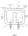
- Fig. 2 is a schematic diagram of a radio frequency (RF) cavity resonator 200 including a radio frequency (RF) conductive medium 205.
- the cavity resonator 200 includes a structural dielectric 210.
- the structural dielectric 210 defines a cavity 216.
- the cavity 216 has an internal geometry corresponding to a desired frequency response characteristic of the cavity resonator 200. In particular, the internal geometry reinforces desired radio frequencies and attenuates undesired radio frequencies.
- the structural dielectric 210 is composed of a material with a low relative permittivity. Also, the material of the structural dielectric 210 has a high conformality potential. For instance, the material of the structure dielectric 210 enables the structural dielectric 210 to conform to complex and smoothly transitioning geometries. The material of the structural dielectric 210 also has high dimensional stability under thermal stress. For example, the material prevents the structural dielectric 210 from deforming under thermal stresses the cavity resonator may experience in typical operational environments. In another embodiment, the material of the structural dielectric 210 has high dimensional stability under mechanical stress such that the material prevents the structural dielectric 210 from denting, flexing, or otherwise mechanically deforming under mechanical stresses experienced in typical operational applications.
- the structural dielectric 210 has an internal surface 211 with a high surface smoothness.
- the internal surface 211 is substantially free from surface irregularities.
- the dielectric surface 211 may a surface smoothness with irregularities having a depth no greater than a depth " ⁇ " at a desired frequency of operation of the radio frequency (RF) cavity resonator 200.
- the cavity resonator 200 also includes an RF input port 230a and RF output port 230b.
- the RF input port 230a and RF output port 230b can be a SubMiniature version A (SMA) connector.
- the RF input port 230a and RF output port 230b can be made of an RF conductive material such as copper, gold, nickel, and silver.
- the RF input port 230a is electrically coupled to a coupling loop 235a.
- the RF input port 230a receives an oscillating RF electromagnetic signal from an RF transmission medium such as a coaxial cable (not shown).
- the RF input port 230a via the coupling loop 235a radiates an oscillating electric and magnetic field (i.e., RF electromagnetic wave) corresponding to the received RF electromagnetic signal.
- the cavity 216 has an internal geometry corresponding to a desired frequency response characteristic of the cavity resonator 200.
- the internal geometry reinforces a range of radio frequencies corresponding to the desired frequency response characteristic of the cavity resonator 200 and attenuates undesired radio frequencies.
- the cavity resonator 200 also includes a resonator element 220.
- the resonator element 220 in this example, is formed by the structural dielectric 210.
- the resonator element 220 can be a separate and distinct structure within the cavity resonator 200.
- the resonator element 220 has a resonant dimension and overall structural geometry that further reinforces desired radio frequencies and attenuates undesired radio frequencies.
- the electromagnetic wave corresponding to the received RF electromagnetic signal induces a resonant mode or modes in the cavity 216. In doing so, the electromagnetic wave interacts with the RF conductive medium 205. In particular, the electromagnetic wave induces an alternating current (AC) in the RF conductive medium 205.
- AC alternating current
- embodiments of the present disclosure provide an RF conductive medium 205 that has a structure and composition giving the RF conductive medium 205 a low effective surface conductive resistivity " R s ". The low surface conductive resistivity " R s " allows the RF conductive medium 205 to support resonant modes in the cavity 216 with a high level of efficiency, thereby increasing the quality factor "Q" of the cavity resonator 200.
- the reinforced frequency of interest induces an AC signal in the coupling loop 235b.
- the AC signal is output from the cavity resonator 200 via the RF output 230b.
- the RF output 230b is electrically coupled to a transmission medium (not shown), which passes the AC signal to an RF hardware component such as an antenna or receiver.
- the RF conductive medium 205 can also include a protective layer (e.g., layer 306 of Fig. 4 ) covering the RF conductive medium.
- the protective layer can be composed of a material that is non-conductive and minimally absorptive to RF energy at a desired frequency of operation the of the cavity resonator 200.
- the material may be at least one of: a polymer coating and a fiberglass coating.
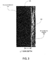
- Fig. 3 is a schematic diagram of a RF conductive medium 305 that is composed of a bundle of discrete conductive nanostructures forming a continuous conductive layer 340 in accordance with an example useful for understanding the invention.
- the RF conductive medium 305 includes a bundle of discrete electrically conductive nanostructures.
- Each of the nanostructures may be made of a nanomaterial that is composed of an element that is at least one of: carbon, silver, copper, aluminum, and gold.
- each of the discrete conductive nanostructures may be a conductive structure that is at least one of: wire, ribbon, tube, and flake.
- the nanomaterial may have a sintering temperature that is a small fraction of a melting temperature of the material on a macro scale. For example, Silver (Ag) melts at 961° C, while nano Silver (Ag) may sinter well below 300° C.
- the RF conductive medium 305 includes a bonding agent (not shown) enabling the bundle of discrete conductive nanostructures to be applied to a surface 345 of the structural dielectric 310.
- the bundle of discrete conductive nanostructures forms the continuous conductive layer 340 in response to being sintered by a heat source.
- the size of each of the discrete electrically conductive nanostructures may be chosen such that the continuous conductive layer 340 has a uniform conductive cross-sectional area that is no greater than a skin depth " ⁇ " at a desired frequency of operation of the cavity resonator 200.
- the continuous conductive layer 340 has a uniform lattice structure and uniform conductive cross-sectional area.
- the heat source may apply a stimulation of heat based on an atomic structure and thickness of nanomaterial of each discrete conductive nanostructure of the bundle of discrete conductive nanostructures.
- the temperature of heat applied by the heat source and the length of time the heat is applied is a function of the atomic structure and thickness of nanomaterial of each discrete conductive nanostructure of the bundle of discrete conductive nanostructures.
- Any heat source known or yet to be known in the art may be used.
- an RF electromagnetic wave induces an alternating current (AC) in the RF conductive medium 305.
- AC alternating current
- DC direct current
- a direct current may propagate throughout an entire volume of a conductor; an alternating current (such as that produced by an RF electromagnetic wave) propagates only within a bounded area very close to a surface of the conductive medium.
- This tendency of alternating currents to propagate near the surface of a conductor is known as "skin effect.”
- skin effect reduces the usable conductive cross sectional area to an extremely thin layer at the surface of the cavity's inner structure.
- skin effect is at least one significant mechanism for RF conduction loss in a resonant cavity, reducing the cavity's Q factor.
- the continuous conductive layer 340 may have a uniform conductive cross-sectional area that is no greater than a skin depth " ⁇ " at a desired frequency of operation of a cavity resonator (e.g., the cavity resonator 200 of Fig. 2 ).
- Table 1 illustrates an example application of EQN.
- the continuous conductive layer 340 may have a uniform conductive cross-sectional area having a skin depth of 50 nm - 4000 nm. In another embodiment, the continuous conductive layer 340 may have a uniform conductive cross-sectional area having a skin depth of 1000 nm- 3000 nm. In yet another example, the continuous conductive layer 340 may have a uniform conductive cross-sectional area having a skin depth of 1500 nm - 2500 nm.
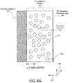
- Fig. 4A is a cross-sectional view an RF conductive medium 405 applied onto a surface 445 of a structural dielectric 410.
- the cross-sectional view is in an orientation such that the axis 475 (i.e., going to right to left on the figure) is an axis perpendicular to a transverse electromagnetic axis 480 (i.e., an axis going into the figure).
- the RF conductive medium 405 includes a diversity of conductive media 470.
- the diversity of conductive media 470 form a plurality of continuous conductive pathways (e.g., continuous conductive pathways 490a-n of Fig. 4B ) in the transverse electromagnetic axis 480.
- Each medium of the diversity of RF conductive media 470 is made of a nanomaterial composed of an element that Is at least one of: silver, copper, aluminum, carbon, and graphene.
- each medium of the diversity of conductive media 470 has a structure that is at least one of wire, ribbon, tube, and flake.
- each conductive medium in the diversity of conductive media 470 is at least one of: single walled carbon nanotubes (SWCNTs), multi-walled nanotubes (MWCNTs), and graphene.
- each of the plurality of continuous conductive pathways 490a-n may have a conductive cross-sectional area no greater than skin depth at a desired frequency of operation of, for example, a cavity resonator (e.g., the cavity resonator 200 of Fig. 2 ).
- the skin depth " ⁇ " may be calculated per EQN. 4.
- each of the plurality of continuous conductive pathways may have a uniform conductive cross-sectional area having a skin depth of 50 nm - 4000 nm. In other examples, each of the plurality of continuous conductive pathways may have a uniform conductive cross-sectional area having a skin depth of 1000 nm - 3000 nm. In yet another example, each of the plurality of continuous conductive pathways may have a uniform conductive cross-sectional area having a skin depth of 1500 nm - 2500 nm.
- the desired frequency of operation "f' may also correspond to at least one of: a desired resonant frequency of an antenna, a cutoff frequency of a waveguide, a desired operational frequency range of a coaxial cable, and combined operational frequency ranges of an integrated structure including a cavity filter and an antenna.
- a suspension dielectric 460 periodically surrounds each of the plurality of the plurality of conductive pathways 490a-n in the transverse electromagnetic axis.
- the suspension dielectric 460 periodically insulates each of the plurality of conductive pathways 490a-n from propagating RF energy in the axis 475 (i.e., the axis perpendicular to the transverse electromagnetic axis 480).
- the suspension dielectric 460 can also be configured to provide mechanical support for each of the plurality of conductive pathways 490a-n.
- each medium of the diversity of RF conductive media 470 is made of a nanomaterial composed of an element that is at least one of: silver, copper, and aluminum
- the suspension dielectric 460 is composed of a structurally rigid and thermally stable material that is weakly interactive with RF energy at the desired frequency of operation.
- each medium of the diversity of RF conductive media 470 is made of a nanomaterial composed of an element that is at least one of: carbon and graphene
- the suspension dielectric 460 is air.
- the suspension dielectric 460 can be composed of air because, for example, single walled carbon nanotubes (SWCNTs), multi-walled nanotubes (MWCNTs), and graphene are materials that are inherently conductive in the transverse electromagnetic axis 480 and weakly conductive in the axis 475.
- the RF conductive medium 405 includes an RF transparent protective layer 450.
- the RF transparent protective layer 450 covers the plurality of continuous conductive pathways 490a-n.
- the protective layer 405 includes a material that is non-conductive and minimally absorptive to RF energy at a desired frequency of operation of, for example, a cavity resonator (e.g., the cavity resonator 200 of Fig. 2 ).
- the material can be at least one of a polymer coating and fiberglass coating.
- the RF conductive medium 405 includes the RF transparent protective layer 450, other example embodiments of the RF conductive medium 405 may not include the RF transparent protective layer 450.
- the RF conductive medium 405 may also include a binding agent (not shown).
- the binding agent is configured to bind the RF conductive medium 405 to the surface 445 of the structural dielectric 410.
- the RF conductive medium 405 may also include a solvent (not shown).
- the solvent is configured to maintain the RF conductive medium 405 in a viscous state during application of the RF conductive medium 405 onto the surface 445.
- the solvent is further configured to evaporate in response to being stimulated by a heat source.
- the heat source in an example, can be an ambient temperature of air surrounding the RF conductive medium 405.
- Fig. 4B is a cross-sectional view the RF conductive medium 405 applied onto a surface 445 of a structural dielectric 410.
- the cross-sectional view is in an orientation such that the axis 475 (i.e., going up and down on the figure) is an axis perpendicular to a transverse electromagnetic axis 480 (i.e., an axis going left to right on the figure).
- the plurality of continuous conductive pathways 490a- n is oriented in the transverse electromagnetic axis 480, such that RF electromagnetic waves induce alternating currents that only predominately travel in the transverse electromagnetic axis 480 along each of the pathways 490a- n .
- the suspension dielectric 460 In order for the alternating current to only predominately travel in the transverse electromagnetic axis 480 along each of the pathways 490a-n, the suspension dielectric 460 periodically surrounds each of the plurality of conductive pathways 490a-n. In particular, the suspension dielectric periodically insulates each of the plurality of conductive pathways 490a- n from propagating RF energy (e.g., alternating current), in the axis 475. At certain points, for example point 495, the suspension dielectric 460 provides avenues for the RF energy to pass from one pathway (e.g., pathway 409b) to another pathway (e.g., pathway 490 n ).
- RF energy e.g., alternating current
- each of the continuous conductive pathways 490a- n has a conductive cross-sectional area no greater than a skin depth " ⁇ " at a desired frequency of operation of an RF device (e.g., the cavity resonator 200 of Fig. 2 )
- the periodic RF insulation provided by the suspension dielectric 460 enables the RF conductive medium 405 to have an increased cross sectional area for RF conductivity, whose constituent elements (e.g., pathways 490a-n) do not suffer from skin effect loss.
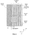
- Fig. 5 is a cross-sectional view of an RF conductive medium 505 that includes an RF transparent protective layer 550 (e.g., protective layer 450 of Figs. 4A-B ) applied to a surface 545 of a structural dielectric 510 of an RF device (e.g., the cavity resonator 200 of Fig. 2 ).
- the cross-sectional view is in an orientation such that the axis 575 (i.e., going right to left on the figure) is an axis perpendicular to a transverse electromagnetic axis 580 (i.e., an axis going up and down on the figure).
- the RF conductive medium 505 includes a plurality of continuous conductive pathways 590 oriented in the transverse electromagnetic axis 580, such that RF electromagnetic waves induce alternating currents that predominately only travel in the transverse electromagnetic axis 580 along each of the pathways 590a- n .
- a diversity of conductive media is structured and periodically arranged to form a structured arrangement of the plurality of continuous conductive pathways 590.
- Each of the plurality of continuous conductive pathways 590 is periodically insulated from a neighboring continuous conductive pathway by a dielectric medium 560 (e.g., a suspension dielectric 460 of Figs. 4A-B ).
- the dielectric medium 560 periodically insulates each of the plurality of conductive pathways 590 from propagating RF energy (e.g., alternating current), in the axis 575.
- RF energy e.g., alternating current
- an RF short 595 provides avenues for the RF energy to pass from one pathway to another pathway.
- a single RF short 595 that traverses each of the plurality of continuous conductive pathways 590 is illustrated in Fig. 5 .
- periodically staggered RF shorts are provided between each of the plurality of continuous conductive pathways.
- each of the continuous conductive pathways 590 has a conductive cross-sectional area no greater than a skin depth " ⁇ " at a desired frequency of operation of an RF device (e.g., the cavity resonator 200 of Fig. 2 )
- the periodic RF insulation provided by the dielectric medium 560 enables the RF conductive medium 505 to have an increased cross sectional area for RF conductivity, whose constituent elements (e.g., pathways 590) do not suffer from skin effect loss.
Description
- Electromagnetic waves or electromagnetic radiation (EMR) is a form of energy that has both electric and magnetic field components. Electromagnetic waves can have many different frequencies.
- Modern telecommunication systems manipulate electromagnetic waves in the electromagnetic spectrum in order to provide wireless communications to subscribers of the telecommunication systems. In particular, modern telecommunication systems manipulate those waves having a frequency categorizing them as Radio Frequency (RF) waves. In order to utilize RF waves, telecommunication systems utilize certain essential hardware components, such as filters, mixers, amplifiers, and antennas.
- The publication
US 2009/0117269 A1 discloses an electrically conductive composite material including metallic nanostrands distributed throughout a matrix constructed of a polymer, ceramic, or elastomer. - The technology described herein relates to a radio frequency (RF) conductive medium for improving the conductive efficiency of an RF device. The RF conductive medium improves the conductive efficiency of the RF device by including one or more conductive pathways in a transverse electromagnetic axis that is free from the loss inducing impact of skin effect at the radio frequencies of interest.
- The main embodiment of the invention is defined in
claim 1. - In an embodiment, each of the plurality of continuous conductive pathways may be a conductive layer in a plurality of conductive layers of conductive pathways. Each of the plurality of conductive layers may be structured and have uniform position or arrangement with respect to other layers of the plurality of conductive layers. In another embodiment, each of the plurality of conductive layers may be unstructured and have a mesh arrangement with respect to other layers of the plurality of conductive layers.
- In some embodiments, the transverse electromagnetic axis is an axis parallel to a surface upon which the RF conductive medium is applied. In other embodiments the transverse electromagnetic axis is an axis that is coplanar to a surface upon which the RF conductive medium is applied.
- The RF conductive medium may also include a solvent configured to maintain the RF conductive medium in a viscous state during application of the RF conductive medium onto a dielectric surface. The solvent is configured to evaporate in response to being stimulated by a heat source.
- Each medium of the diversity of conductive media may be made of a nanomaterial composed of an element that is at least one of: silver, copper, aluminum, and gold. Also, each medium of the diversity of conductive media may have a structure that is at least one of: wire, ribbon, tube, and flake.
- In addition, each of the plurality of continuous conductive pathways may have a conductive cross-sectional area no greater than skin depth at a desired frequency of operation. In an embodiment, the skin depth "δ" may be calculated by:

- The desired frequency of operation may correspond to at least one of: a desired resonant frequency of a cavity filter, a desired resonant frequency of an antenna, a cutoff frequency of a waveguide, a desired operational frequency range of a coaxial cable, and combined operational frequency ranges of an integrated structure including a cavity filter and an antenna.
- Each of the plurality of continuous conductive pathways may have a uniform conductive cross-sectional area having a skin depth of 50 nm - 4000 nm. In other examples, each of the plurality of continuous conductive pathways may have a uniform conductive cross-sectional area having a skin depth of 1000 nm - 3000 nm. In yet another example, each of the plurality of continuous conductive pathways may have a uniform conductive cross-sectional area having a skin depth of 1500 nm - 2500 nm.
- The RF conductive medium may also include a protective layer covering the plurality of layers of continuous conductive pathways, where the protective layer includes a material that is non-conductive and minimally absorptive to RF energy at a desired frequency of operation. The material may be at least one of: a polymer coating and fiberglass coating.
- In a sub-embodiment, the suspension dielectric comprises a layer of RF inert material which is non-conductive and minimally absorptive to RF energy ata desired frequency of operation. Also, the layer of RF inert material is configured to secure the diversity of conductive media onto a dielectric surface. The RF inert material may be at least one of: a polymer coating and fiberglass coating.
- The RF conductive medium may also include a binding agent to bind the RF conductive medium to the surface. The RF conductive medium may further include a solvent configured to maintain the RF conductive medium in a viscous state during application of the RF conductive medium onto the dielectric surface. The solvent further is configured to evaporate in response to being stimulated by a heat source.
- Each medium of the diversity of conductive media may be made of a nanomaterial composed of an element that is at least one of: carbon and graphene.
- The dielectric surface may be an inner surface of a cavity having an internal geometry corresponding to a desired frequency response characteristic of the cavity. In another embodiment, the bundle of discrete nanostructures may be applied to an outer surface of a first dielectric surface and to a concentric inner surface of a second dielectric surface. The first dielectric surface is an inner conductor and the second dielectric surface is an outer conductor of a coaxial cable. Also, the bundle of discrete conductive nanostructures may be applied to a dielectric structure, where the geometry of the dielectric structure and conductive properties of the bundle of discrete conductive nanostructures define a resonant frequency response and radiation pattern of an antenna.
- The foregoing will be apparent from the following more particular description of example embodiments of the disclosure, as illustrated in the accompanying drawings in which like reference characters refer to the same parts throughout the different views. The drawings are not necessarily to scale, emphasis instead being placed upon illustrating embodiments of the present disclosure.
-
Fig. 1 is a schematic diagram of a rectangular waveguide cavity in accordance with an example embodiment of the present disclosure; -
Fig. 2 is a schematic diagram of a cavity resonator including a radio frequency (RF) conductive medium in accordance with an example embodiment of the present disclosure; -
Fig. 3 is a schematic diagram of a RF conductive medium that is composed of a bundle of discrete conductive nanostructures forming a continuous conductive layer in accordance with an example useful for understanding the invention; -
Figs. 4A-B are cross-sectional views of an RF conductive medium applied onto a surface of a structural dielectric in accordance with an example useful for understanding the invention; and -
Fig. 5 is a cross-sectional view of a highly structured RF conductive medium applied onto a surface of a structural dielectric in accordance with an example useful for understanding the invention. - A description of example embodiments of the disclosure follows.
- Modern telecommunication systems manipulate electromagnetic waves having a range of wavelengths in the electromagnetic spectrum that categorize them as Radio Frequency (RF) waves. In order to utilize RF waves, telecommunication systems employ certain essential RF hardware components such as filters, mixers, amplifiers, and antennas.
- The RF hardware components interact with the RF waves via RF conductive elements. The RF conductive elements are generally composed of an RF conductive medium, such as, aluminum, copper, silver, and gold. However, the structures of conventional RF conductive media suffer from effective electrical resistance thatimpedes the conduction of RF energy, introducing undesirable insertion loss into all RF hardware components and lowering the Q factor of specific RF hardware components like resonant cavity filters.
- The principal physical mechanism for undesirable loss in the conduction of RF energy through RF hardware components is skin effect. Skin effect occurs due to counter-electromotive force in a conductor, which is a consequence of the alternating electron currents in the conductive medium induced by applied RF energy. As its name suggests, skin effect causes the majority of electron current to flow at the surface of the conductor, a region defined as the "skin depth." Skin effect reduces the effective cross sectional area of a conductor, often to a small fraction of its physical cross section. The effective skin depth of a conductor is a frequency dependent quality, which is inversely proportional to wavelength. This means that the higher the frequency, the more shallow the skin depth and, by extension, the greater the effective RF conduction loss.
- The technology described herein relates to a radio frequency (RF) conductive medium (hereinafter, "technology") for reducing the RF conduction loss of an RF hardware component. The RF conductive medium created by this technology reduces the RF conduction loss of the RF device by frustrating the formation of counter-electromotive force in the conductor.
- For context and without limitation, the technology herein is described in the context of an RF cavity resonator. However, it should be noted that the technology can be applied to any RF component requiring an RF conductive medium configured to interact with RF waves. For example, the RF component can be an antenna, waveguide, coaxial cable, and an integrated structure including a cavity filter and an antenna.
-
Fig. 1 is a schematic diagram of a rectangular radio frequency (RF)waveguide cavity filter 101. TheRF cavity filter 101, as most RF cavity resonators, is typically defined as a "closed metallic structure" that confines radio frequency electromagnetic fields in acavity 100 defined bywalls 110a-n. Thecavity filter 101 acts as a low loss resonant circuit with a specific frequency response and is analogous to a classical resonant circuit composed of discrete inductive (L) and capacitive (C) components. However, unlike conventional LC circuits, thecavity filter 101 exhibits extremely low energy loss at the filter's design wavelength (i.e., physical internal geometry of the cavity filter 101). This means that the Q factor of thecavity filter 101 is hundreds of times greater than that of a discrete component resonator such as an LC "tank" circuit. - The Q factor of any resonant circuit or structure (e.g., cavity filter 101) measures the degree to which the resonant circuit or structure damps energy applied to it. Thus, Q factor may be expressed as a ratio of energy stored in the resonant circuit or structure to energy dissipated in the resonant circuit or structure per oscillation cycle. The less energy dissipated per cycle, the higher the Q factor. For example, the Q factor "Q" can be defined by:

- The Q factor of the
cavity filter 101 is influenced by two factors: (a) power losses in adielectric medium 115 of thecavity filter 101 and (b) power losses in thewalls 110a-n of thecavity filter 101. In practical applications of cavity resonator based filters such ascavity filter 101, thedielectric medium 115 is often air. Losses induced by air can be considered miniscule at the frequencies in the lower microwave spectrum commonly used for mobile broadband communications. Thus, conductor losses in thewalls 110a-n of thecavity filter 101 contribute most to lower effective Q factor and higher insertion loss of thecavity filter 101. - For instance, the Q factor "Q" of the
cavity filter 101 can be defined by:
- As stated above, the RF conduction losses of the dielectric medium (e.g., air) 115 is negligible because RF energy in the lower microwave spectrum is weakly interactive with air and other common cavity dielectrics. Thus, the RF conductivity of the
walls 110a-n "Qc" of thecavity filter 101 contributes most to the quality factor "Q" of thecavity filter 101. The quality factor contribution of the RF conductivity of thewalls 110a-n "Qc" can be defined by:
cavity walls 110a-n, and a / b l d are physical dimensions of thecavity filter 101. Thus, an increasing value of surface resistivity "Rs" of the cavity walls 110an decreases the value of Qc, thereby, reducing the Q factor of thecavity filter 101. - In order to increase the Q factor of the
cavity filter 101 and other RF device, embodiments of the present invention provide a RF conductive medium that reduces the surface resistivity "Rs" of RF conductive elements of RF devices such as thecavity filter 101. -
Fig. 2 is a schematic diagram of a radio frequency (RF)cavity resonator 200 including a radio frequency (RF)conductive medium 205. Thecavity resonator 200 includes astructural dielectric 210. Thestructural dielectric 210 defines acavity 216. Thecavity 216 has an internal geometry corresponding to a desired frequency response characteristic of thecavity resonator 200. In particular, the internal geometry reinforces desired radio frequencies and attenuates undesired radio frequencies. - The
structural dielectric 210 is composed of a material with a low relative permittivity. Also, the material of thestructural dielectric 210 has a high conformality potential. For instance, the material of thestructure dielectric 210 enables thestructural dielectric 210 to conform to complex and smoothly transitioning geometries. The material of thestructural dielectric 210 also has high dimensional stability under thermal stress. For example, the material prevents thestructural dielectric 210 from deforming under thermal stresses the cavity resonator may experience in typical operational environments. In another embodiment, the material of thestructural dielectric 210 has high dimensional stability under mechanical stress such that the material prevents thestructural dielectric 210 from denting, flexing, or otherwise mechanically deforming under mechanical stresses experienced in typical operational applications. - In addition, the
structural dielectric 210 has aninternal surface 211 with a high surface smoothness. In particular, theinternal surface 211 is substantially free from surface irregularities. In an embodiment, thedielectric surface 211 may a surface smoothness with irregularities having a depth no greater than a depth "δ" at a desired frequency of operation of the radio frequency (RF)cavity resonator 200. - The
cavity resonator 200 also includes anRF input port 230a andRF output port 230b. In an example, theRF input port 230a andRF output port 230b can be a SubMiniature version A (SMA) connector. TheRF input port 230a andRF output port 230b can be made of an RF conductive material such as copper, gold, nickel, and silver. - The
RF input port 230a is electrically coupled to acoupling loop 235a. TheRF input port 230a receives an oscillating RF electromagnetic signal from an RF transmission medium such as a coaxial cable (not shown). In response to receiving the oscillating RF electromagnetic signal, theRF input port 230a via thecoupling loop 235a radiates an oscillating electric and magnetic field (i.e., RF electromagnetic wave) corresponding to the received RF electromagnetic signal. - As stated herein, the
cavity 216 has an internal geometry corresponding to a desired frequency response characteristic of thecavity resonator 200. In particular, the internal geometry reinforces a range of radio frequencies corresponding to the desired frequency response characteristic of thecavity resonator 200 and attenuates undesired radio frequencies. In addition, thecavity resonator 200 also includes aresonator element 220. Theresonator element 220, in this example, is formed by thestructural dielectric 210. However, it should be noted that theresonator element 220 can be a separate and distinct structure within thecavity resonator 200. Theresonator element 220 has a resonant dimension and overall structural geometry that further reinforces desired radio frequencies and attenuates undesired radio frequencies. - The electromagnetic wave corresponding to the received RF electromagnetic signal induces a resonant mode or modes in the
cavity 216. In doing so, the electromagnetic wave interacts with the RFconductive medium 205. In particular, the electromagnetic wave induces an alternating current (AC) in the RFconductive medium 205. As described herein, embodiments of the present disclosure provide an RF conductive medium 205 that has a structure and composition giving the RF conductive medium 205 a low effective surface conductive resistivity "Rs ". The low surface conductive resistivity "Rs" allows the RF conductive medium 205 to support resonant modes in thecavity 216 with a high level of efficiency, thereby increasing the quality factor "Q" of thecavity resonator 200. - The reinforced frequency of interest induces an AC signal in the
coupling loop 235b. The AC signal is output from thecavity resonator 200 via theRF output 230b. TheRF output 230b is electrically coupled to a transmission medium (not shown), which passes the AC signal to an RF hardware component such as an antenna or receiver. - The RF conductive medium 205 can also include a protective layer (e.g., layer 306 of
Fig. 4 ) covering the RF conductive medium. The protective layer can be composed of a material that is non-conductive and minimally absorptive to RF energy at a desired frequency of operation the of thecavity resonator 200. The material may be at least one of: a polymer coating and a fiberglass coating. -
Fig. 3 is a schematic diagram of a RF conductive medium 305 that is composed of a bundle of discrete conductive nanostructures forming a continuousconductive layer 340 in accordance with an example useful for understanding the invention. - The RF
conductive medium 305 includes a bundle of discrete electrically conductive nanostructures. Each of the nanostructures may be made of a nanomaterial that is composed of an element that is at least one of: carbon, silver, copper, aluminum, and gold. Also, each of the discrete conductive nanostructures may be a conductive structure that is at least one of: wire, ribbon, tube, and flake. The nanomaterial may have a sintering temperature that is a small fraction of a melting temperature of the material on a macro scale. For example, Silver (Ag) melts at 961° C, while nano Silver (Ag) may sinter well below 300° C. - In addition, the RF
conductive medium 305 includes a bonding agent (not shown) enabling the bundle of discrete conductive nanostructures to be applied to asurface 345 of thestructural dielectric 310. The bundle of discrete conductive nanostructures forms the continuousconductive layer 340 in response to being sintered by a heat source. The size of each of the discrete electrically conductive nanostructures may be chosen such that the continuousconductive layer 340 has a uniform conductive cross-sectional area that is no greater than a skin depth "δ" at a desired frequency of operation of thecavity resonator 200. The continuousconductive layer 340 has a uniform lattice structure and uniform conductive cross-sectional area. The heat source may apply a stimulation of heat based on an atomic structure and thickness of nanomaterial of each discrete conductive nanostructure of the bundle of discrete conductive nanostructures. For example, the temperature of heat applied by the heat source and the length of time the heat is applied is a function of the atomic structure and thickness of nanomaterial of each discrete conductive nanostructure of the bundle of discrete conductive nanostructures. Any heat source known or yet to be known in the art may be used. - As stated above, an RF electromagnetic wave induces an alternating current (AC) in the RF
conductive medium 305. For AC, an influence of the structure's cross sectional area on AC resistance is radically different than for direct current (DC) resistance. For example, a direct current may propagate throughout an entire volume of a conductor; an alternating current (such as that produced by an RF electromagnetic wave) propagates only within a bounded area very close to a surface of the conductive medium. This tendency of alternating currents to propagate near the surface of a conductor is known as "skin effect." In an RF device, such as thecavity resonator 200, skin effect reduces the usable conductive cross sectional area to an extremely thin layer at the surface of the cavity's inner structure. Thus, skin effect is at least one significant mechanism for RF conduction loss in a resonant cavity, reducing the cavity's Q factor. - Thus, the continuous
conductive layer 340 may have a uniform conductive cross-sectional area that is no greater than a skin depth "δ" at a desired frequency of operation of a cavity resonator (e.g., thecavity resonator 200 ofFig. 2 ). In an embodiment, the skin depth "δ" may be calculated by:
Table 1 Frequency 700 MHz 800 MHz 1900 MHz 2100 MHz 2500 MHz Skin Depth 2870 nm 2690 nm 1749 nm 11660 nm 1520 nm - In an embodiment, the continuous
conductive layer 340 may have a uniform conductive cross-sectional area having a skin depth of 50 nm - 4000 nm. In another embodiment, the continuousconductive layer 340 may have a uniform conductive cross-sectional area having a skin depth of 1000 nm- 3000 nm. In yet another example, the continuousconductive layer 340 may have a uniform conductive cross-sectional area having a skin depth of 1500 nm - 2500 nm. -
Fig. 4A is a cross-sectional view an RF conductive medium 405 applied onto asurface 445 of astructural dielectric 410. In particular, the cross-sectional view is in an orientation such that the axis 475 (i.e., going to right to left on the figure) is an axis perpendicular to a transverse electromagnetic axis 480 (i.e., an axis going into the figure). The RFconductive medium 405 includes a diversity ofconductive media 470. The diversity ofconductive media 470 form a plurality of continuous conductive pathways (e.g., continuousconductive pathways 490a-n ofFig. 4B ) in the transverseelectromagnetic axis 480. - Each medium of the diversity of RF
conductive media 470 is made of a nanomaterial composed of an element that Is at least one of: silver, copper, aluminum, carbon, and graphene. In an example where the element is at least one of: silver, copper, and aluminum, each medium of the diversity ofconductive media 470 has a structure that is at least one of wire, ribbon, tube, and flake. In an example where the element is at least one of: carbon and graphene, each conductive medium in the diversity ofconductive media 470 is at least one of: single walled carbon nanotubes (SWCNTs), multi-walled nanotubes (MWCNTs), and graphene. - Also, each of the plurality of continuous
conductive pathways 490a-n may have a conductive cross-sectional area no greater than skin depth at a desired frequency of operation of, for example, a cavity resonator (e.g., thecavity resonator 200 ofFig. 2 ). In an embodiment, the skin depth "δ" may be calculated per EQN. 4. - In an embodiment, each of the plurality of continuous conductive pathways may have a uniform conductive cross-sectional area having a skin depth of 50 nm - 4000 nm. In other examples, each of the plurality of continuous conductive pathways may have a uniform conductive cross-sectional area having a skin depth of 1000 nm - 3000 nm. In yet another example, each of the plurality of continuous conductive pathways may have a uniform conductive cross-sectional area having a skin depth of 1500 nm - 2500 nm.
- It should be noted that the desired frequency of operation "f' may also correspond to at least one of: a desired resonant frequency of an antenna, a cutoff frequency of a waveguide, a desired operational frequency range of a coaxial cable, and combined operational frequency ranges of an integrated structure including a cavity filter and an antenna.
- A
suspension dielectric 460 periodically surrounds each of the plurality of the plurality ofconductive pathways 490a-n in the transverse electromagnetic axis. In particular, thesuspension dielectric 460 periodically insulates each of the plurality ofconductive pathways 490a-n from propagating RF energy in the axis 475 (i.e., the axis perpendicular to the transverse electromagnetic axis 480). Thesuspension dielectric 460 can also be configured to provide mechanical support for each of the plurality ofconductive pathways 490a-n. - In an example embodiment where each medium of the diversity of RF
conductive media 470 is made of a nanomaterial composed of an element that is at least one of: silver, copper, and aluminum, thesuspension dielectric 460 is composed of a structurally rigid and thermally stable material that is weakly interactive with RF energy at the desired frequency of operation. - In another example useful for understanding the invention where each medium of the diversity of RF
conductive media 470 is made of a nanomaterial composed of an element that is at least one of: carbon and graphene, thesuspension dielectric 460 is air. In such a case, thesuspension dielectric 460 can be composed of air because, for example, single walled carbon nanotubes (SWCNTs), multi-walled nanotubes (MWCNTs), and graphene are materials that are inherently conductive in the transverseelectromagnetic axis 480 and weakly conductive in theaxis 475. - In this example, the RF
conductive medium 405 includes an RF transparentprotective layer 450. The RF transparentprotective layer 450 covers the plurality of continuousconductive pathways 490a-n. Theprotective layer 405 includes a material that is non-conductive and minimally absorptive to RF energy at a desired frequency of operation of, for example, a cavity resonator (e.g., thecavity resonator 200 ofFig. 2 ). In an example embodiment, the material can be at least one of a polymer coating and fiberglass coating. Although, in this example, the RFconductive medium 405 includes the RF transparentprotective layer 450, other example embodiments of the RFconductive medium 405 may not include the RF transparentprotective layer 450. - The RF
conductive medium 405 may also include a binding agent (not shown). The binding agent is configured to bind the RF conductive medium 405 to thesurface 445 of thestructural dielectric 410. In addition, the RFconductive medium 405 may also include a solvent (not shown). The solvent is configured to maintain the RF conductive medium 405 in a viscous state during application of the RF conductive medium 405 onto thesurface 445. The solvent is further configured to evaporate in response to being stimulated by a heat source. The heat source, in an example, can be an ambient temperature of air surrounding the RFconductive medium 405. -
Fig. 4B is a cross-sectional view the RF conductive medium 405 applied onto asurface 445 of astructural dielectric 410. In particular, the cross-sectional view is in an orientation such that the axis 475 (i.e., going up and down on the figure) is an axis perpendicular to a transverse electromagnetic axis 480 (i.e., an axis going left to right on the figure). As illustrated, the plurality of continuousconductive pathways 490a-n is oriented in the transverseelectromagnetic axis 480, such that RF electromagnetic waves induce alternating currents that only predominately travel in the transverseelectromagnetic axis 480 along each of thepathways 490a-n. - In order for the alternating current to only predominately travel in the transverse
electromagnetic axis 480 along each of thepathways 490a-n, thesuspension dielectric 460 periodically surrounds each of the plurality ofconductive pathways 490a-n. In particular, the suspension dielectric periodically insulates each of the plurality ofconductive pathways 490a-n from propagating RF energy (e.g., alternating current), in theaxis 475. At certain points, forexample point 495, thesuspension dielectric 460 provides avenues for the RF energy to pass from one pathway (e.g., pathway 409b) to another pathway (e.g.,pathway 490n). - In examples where each of the continuous
conductive pathways 490a-n, as described above, has a conductive cross-sectional area no greater than a skin depth "δ" at a desired frequency of operation of an RF device (e.g., thecavity resonator 200 ofFig. 2 ), the periodic RF insulation provided by thesuspension dielectric 460 enables the RF conductive medium 405 to have an increased cross sectional area for RF conductivity, whose constituent elements (e.g.,pathways 490a-n) do not suffer from skin effect loss. -
Fig. 5 is a cross-sectional view of an RF conductive medium 505 that includes an RF transparent protective layer 550 (e.g.,protective layer 450 ofFigs. 4A-B ) applied to asurface 545 of a structural dielectric 510 of an RF device (e.g., thecavity resonator 200 ofFig. 2 ). In particular, the cross-sectional view is in an orientation such that the axis 575 (i.e., going right to left on the figure) is an axis perpendicular to a transverse electromagnetic axis 580 (i.e., an axis going up and down on the figure). The RFconductive medium 505 includes a plurality of continuousconductive pathways 590 oriented in the transverseelectromagnetic axis 580, such that RF electromagnetic waves induce alternating currents that predominately only travel in the transverseelectromagnetic axis 580 along each of the pathways 590a-n. - A diversity of conductive media is structured and periodically arranged to form a structured arrangement of the plurality of continuous
conductive pathways 590. Each of the plurality of continuousconductive pathways 590 is periodically insulated from a neighboring continuous conductive pathway by a dielectric medium 560 (e.g., asuspension dielectric 460 ofFigs. 4A-B ). Thedielectric medium 560 periodically insulates each of the plurality ofconductive pathways 590 from propagating RF energy (e.g., alternating current), in theaxis 575. At certain points, an RF short 595 provides avenues for the RF energy to pass from one pathway to another pathway. A single RF short 595 that traverses each of the plurality of continuousconductive pathways 590 is illustrated inFig. 5 . According to the main embodiment of the invention, periodically staggered RF shorts are provided between each of the plurality of continuous conductive pathways. - In embodiments where each of the continuous
conductive pathways 590, as described above, has a conductive cross-sectional area no greater than a skin depth "δ" at a desired frequency of operation of an RF device (e.g., thecavity resonator 200 ofFig. 2 ), the periodic RF insulation provided by thedielectric medium 560 enables the RF conductive medium 505 to have an increased cross sectional area for RF conductivity, whose constituent elements (e.g., pathways 590) do not suffer from skin effect loss. - While this disclosure has been particularly shown and described with references to example embodiments thereof, it will be understood by those skilled in the art that various changes in form and details may be made therein without departing from the scope of the disclosure encompassed by the appended claims.
Claims (14)
- A radio frequency (RF) device comprising:a structural dielectric (410);an RF conductive medium (405) on a surface of the structural dielectric (410) for reducing RF conduction loss, the RF conductive medium (405) comprising:a diversity of conductive media (470) forming a plurality of continuous conductive pathways (490a-490n) in a transverse electromagnetic axis (480), with periodically staggered RF shorts between each of the plurality of continuous conductive pathways (490a-490n); anda suspension dielectric (460) surrounding the plurality of continuous conductive pathways (490a-490n) in the transverse electromagnetic axis (480).
- The RF device of claim 1, wherein each medium of the diversity of conductive media is made of a nanomaterial composed of an element that is at least one of: silver, copper, aluminum, and gold.
- The RF device of any of the preceding claims, wherein each medium of the diversity of conductive media has a structure that is at least one of: wire, ribbon, tube, and flake.
- The RF device of preceding claim1, wherein each medium of the diversity of conductive media comprises a nanomaterial that is at least one of carbon or graphene.
- The RF device of any of claims 2-4, wherein the RF conductive medium has a skin depth "δ" calculated by:

- The RF device of claim 5 wherein the frequency of operation corresponds to at least one of: a resonant frequency of a cavity filter, a resonant frequency of an antenna, a cutoff frequency of a waveguide, an operational frequency of a coaxial cable, and an operational frequency of an integrated structure including a cavity filter and an antenna.
- The RF device of any of claims 1-4, wherein each of the plurality of continuous conductive pathways has a skin depth of 50 nm to 4000 nm.
- The RF device of any of claims 1-4, wherein each of the plurality of continuous conductive pathways has a skin depth of 1000 nm to 3000 nm.
- The RF device of any of claims 1-4, wherein each of the plurality of continuous conductive pathways has a skin depth of 1500 nm to 2500 nm.
- The RF device of any of the preceding claims, said RF conductive medium further comprising:a protective layer (450) covering the plurality of continuous conductive pathways,wherein the protective layer includes a material that is non-conductive and minimally absorptive to RF energy at a desired frequency of operation of the RF device.
- The RF device of claim 10, wherein the material is at least one of a polymer coating or a fiberglass coating.
- The RF device of any of the preceding claims, wherein the suspension dielectric comprises a layer of RF inert material surrounding the diversity of conductive media, the RF inert material being non-conductive and minimally absorptive to RF energy at a desired frequency of operation of the RF device, the layer of RF inert material configured to secure the diversity of conductive media onto the structural dielectric.
- The RF device of claim 12 further comprising a binding agent to bind the RF conductive medium to the structural dielectric.
- The RF device of any of the preceding claims, wherein the suspension dielectric is configured to periodically insulate each of the plurality of continuous conductive pathways from propagating RF energy in an axis perpendicular to the transverse electromagnetic axis.
Applications Claiming Priority (4)
| Application Number | Priority Date | Filing Date | Title |
|---|---|---|---|
| US201261640784P | 2012-05-01 | 2012-05-01 | |
| US201361782629P | 2013-03-14 | 2013-03-14 | |
| EP13722915.9A EP2845263B1 (en) | 2012-05-01 | 2013-04-29 | Radio frequency (rf) conductive medium |
| PCT/US2013/038628 WO2013165892A2 (en) | 2012-05-01 | 2013-04-29 | Radio frequency (rf) conductive medium |
Related Parent Applications (1)
| Application Number | Title | Priority Date | Filing Date |
|---|---|---|---|
| EP13722915.9A Division EP2845263B1 (en) | 2012-05-01 | 2013-04-29 | Radio frequency (rf) conductive medium |
Publications (2)
| Publication Number | Publication Date |
|---|---|
| EP3614486A1 EP3614486A1 (en) | 2020-02-26 |
| EP3614486B1 true EP3614486B1 (en) | 2020-04-08 |
Family
ID=48444594
Family Applications (2)
| Application Number | Title | Priority Date | Filing Date |
|---|---|---|---|
| EP13722915.9A Active EP2845263B1 (en) | 2012-05-01 | 2013-04-29 | Radio frequency (rf) conductive medium |
| EP19198693.4A Active EP3614486B1 (en) | 2012-05-01 | 2013-04-29 | Radio frequency (rf) conductive medium |
Family Applications Before (1)
| Application Number | Title | Priority Date | Filing Date |
|---|---|---|---|
| EP13722915.9A Active EP2845263B1 (en) | 2012-05-01 | 2013-04-29 | Radio frequency (rf) conductive medium |
Country Status (5)
| Country | Link |
|---|---|
| US (6) | US9166268B2 (en) |
| EP (2) | EP2845263B1 (en) |
| JP (3) | JP2015523760A (en) |
| CN (2) | CN107425252B (en) |
| WO (1) | WO2013165892A2 (en) |
Families Citing this family (3)
| Publication number | Priority date | Publication date | Assignee | Title |
|---|---|---|---|---|
| US9166268B2 (en) | 2012-05-01 | 2015-10-20 | Nanoton, Inc. | Radio frequency (RF) conductive medium |
| JP2016012798A (en) * | 2014-06-27 | 2016-01-21 | Tdk株式会社 | High frequency transmission line, antenna, and electronic circuit board |
| KR102057314B1 (en) * | 2018-11-26 | 2020-01-22 | 주식회사 센서뷰 | Low loss and Flexible Transmission line integrated multi-port antenna for mmWave band |
Family Cites Families (62)
| Publication number | Priority date | Publication date | Assignee | Title |
|---|---|---|---|---|
| US2769148A (en) * | 1951-03-07 | 1956-10-30 | Bell Telephone Labor Inc | Electrical conductors |
| US2769150A (en) * | 1952-11-14 | 1956-10-30 | Bell Telephone Labor Inc | Laminated conductor |
| US2981908A (en) | 1958-12-15 | 1961-04-25 | Jr Moody C Thompson | Cavity resonator |
| US3760300A (en) * | 1972-07-31 | 1973-09-18 | Westinghouse Electric Corp | Reduced loss phase shifter utilizing faraday rotator |
| EP0290148A3 (en) * | 1987-05-07 | 1990-11-22 | Varian Associates, Inc. | Surface coating with very high rf loss for microwave components |
| US4971856A (en) * | 1987-05-07 | 1990-11-20 | Arthur Karp | Microwave components with a surface coating which imparts a very high RF loss |
| US5213715A (en) * | 1989-04-17 | 1993-05-25 | Western Digital Corporation | Directionally conductive polymer |
| RU2139613C1 (en) * | 1993-08-27 | 1999-10-10 | Мурата Мануфакчуринг Ко., Лтд. | Thin-film multilayer electrode coupled by high-frequency electromagnetic field, high-frequency transmission line, high-frequency resonator, high-frequency filter, high- frequency band-pass rejection filter and high-frequency device |
| JP3314594B2 (en) * | 1995-09-22 | 2002-08-12 | 松下電器産業株式会社 | High frequency circuit electrode, transmission line and resonator using the same |
| US5929727A (en) | 1996-10-11 | 1999-07-27 | Matsushita Electric Industrial Co., Ltd. | Dielectric resonator, method for manufacturing the same, filter and communication apparatus |
| JP3561141B2 (en) * | 1998-03-26 | 2004-09-02 | 京セラ株式会社 | Measurement method of linear expansion coefficient |
| JP2001111312A (en) * | 1999-10-14 | 2001-04-20 | Toyota Central Res & Dev Lab Inc | Waveguide/transmission line converter |
| JP3219067B2 (en) * | 1999-01-08 | 2001-10-15 | 日本電気株式会社 | Integrated circuit |
| JP2001196817A (en) * | 1999-11-05 | 2001-07-19 | Murata Mfg Co Ltd | Dielectric resonator, dielectric filter, dielectric duplexer and communication apparatus |
| US6300850B1 (en) | 2000-01-31 | 2001-10-09 | Tx Rx Systems Inc. | Temperature compensating cavity bandpass filter |
| EP1146591A2 (en) * | 2000-04-10 | 2001-10-17 | Hitachi, Ltd. | Electromagnetic wave absorber, method of manufacturing the same and appliance using the same |
| US6498550B1 (en) | 2000-04-28 | 2002-12-24 | Motorola, Inc. | Filtering device and method |
| US7301199B2 (en) | 2000-08-22 | 2007-11-27 | President And Fellows Of Harvard College | Nanoscale wires and related devices |
| US6677832B1 (en) * | 2000-10-27 | 2004-01-13 | Lucent Technologies Inc. | Connector for differential-mode transmission line providing virtual ground |
| US6650208B2 (en) | 2001-06-07 | 2003-11-18 | Remec Oy | Dual-mode resonator |
| ATE504625T1 (en) * | 2001-11-05 | 2011-04-15 | Radio Frequency Systems Inc | DIELECTRIC MICROCELLULAR FOAM FOR USE IN TRANSMISSION LINES |
| US7935415B1 (en) * | 2002-04-17 | 2011-05-03 | Conductive Composites Company, L.L.C. | Electrically conductive composite material |
| AU2003225074A1 (en) * | 2002-04-17 | 2003-11-03 | Silicon Pipe, Inc. | Signal transmission line structure with an air dielectric |
| JP4097069B2 (en) * | 2002-08-28 | 2008-06-04 | Tdk株式会社 | Printed circuit board manufacturing method |
| US20050007001A1 (en) | 2003-01-24 | 2005-01-13 | Imholt Timothy James | Process and apparatus for energy storage and release |
| WO2005008305A1 (en) * | 2003-07-18 | 2005-01-27 | Nippon Sheet Glass Company, Limited | Photonic crystal waveguide, homogeneous medium waveguide, and optical device |
| US6997039B2 (en) | 2004-02-24 | 2006-02-14 | Clemson University | Carbon nanotube based resonant-circuit sensor |
| US7224248B2 (en) | 2004-06-25 | 2007-05-29 | D Ostilio James P | Ceramic loaded temperature compensating tunable cavity filter |
| FR2874126B1 (en) | 2004-08-06 | 2006-11-17 | Lionel Girardie | TECHNICAL MANUFACTURING OF NANO-SYSTEMS FOR RF FILTER AND ENERGY EXCHANGER |
| JP2007088917A (en) * | 2005-09-22 | 2007-04-05 | Tdk Corp | Transmission line, electronic component, and manufacturing method of the transmission line |
| EP1811596B1 (en) * | 2006-01-20 | 2011-09-07 | Alcatel Lucent | Radio frequency waveguide comprising an electric conductor made of a plastic foil layer laminated with an electric conductive material layer |
| US7453154B2 (en) * | 2006-03-29 | 2008-11-18 | Delphi Technologies, Inc. | Carbon nanotube via interconnect |
| CN102324462B (en) * | 2006-10-12 | 2015-07-01 | 凯博瑞奥斯技术公司 | Nanowire-based transparent conductors and applications thereof |
| JP2008287974A (en) * | 2007-05-16 | 2008-11-27 | Auto Network Gijutsu Kenkyusho:Kk | Contact device, and glass antenna device |
| US20090160728A1 (en) * | 2007-12-21 | 2009-06-25 | Motorola, Inc. | Uncorrelated antennas formed of aligned carbon nanotubes |
| US7795536B2 (en) * | 2008-01-18 | 2010-09-14 | Temp-Flex Cable, Inc. | Ultra high-speed coaxial cable |
| US8248305B2 (en) * | 2008-06-03 | 2012-08-21 | University Of Houston | Antennas based on a conductive polymer composite and methods for production thereof |
| US20090315644A1 (en) | 2008-06-19 | 2009-12-24 | Honeywell International Inc. | High-q disk nano resonator device and method of fabricating the same |
| CN102203949B (en) | 2008-07-25 | 2014-10-22 | 特拉维夫大学拉莫特有限公司 | Rectifying antenna device, rectifying antenna system and method for preparing rectifying antenna device |
| WO2010013982A2 (en) * | 2008-08-01 | 2010-02-04 | Kmw Inc. | Dielectric resonator in rf filter and assembly method therefor |
| KR101072284B1 (en) * | 2008-08-01 | 2011-10-11 | 주식회사 케이엠더블유 | Dielectric resonator in radio frequency filter and assembling thereof |
| US9024709B2 (en) | 2008-10-03 | 2015-05-05 | Purdue Research Foundation | Tunable evanescent-mode cavity filter |
| CN102187514A (en) * | 2008-10-20 | 2011-09-14 | 斯盖沃克斯瑟路申斯公司 | Magnetic-dielectric assemblies and methods of fabrication |
| US8130167B2 (en) * | 2009-04-10 | 2012-03-06 | Coi Ceramics, Inc. | Radomes, aircraft and spacecraft including such radomes, and methods of forming radomes |
| JP5278210B2 (en) * | 2009-07-13 | 2013-09-04 | ソニー株式会社 | Wireless transmission system, electronic equipment |
| IT1394959B1 (en) * | 2009-07-28 | 2012-07-27 | St Microelectronics Srl | MANUFACTURE OF VERTICAL INTERCONNECTIONS IN INTEGRATION STACKS, CONTACT FROM UPPER METAL METAL DEPOSITOR |
| TWI420540B (en) * | 2009-09-14 | 2013-12-21 | Ind Tech Res Inst | Conductive material formed using light or thermal energy and method for manufacturing the same, and nano-scale composition |
| US20120055013A1 (en) | 2010-07-13 | 2012-03-08 | Féinics AmaTech Nominee Limited | Forming microstructures and antennas for transponders |
| JP5428924B2 (en) * | 2010-02-16 | 2014-02-26 | 東レ株式会社 | Conductive laminate and touch panel using the same |
| KR20130010471A (en) * | 2010-02-27 | 2013-01-28 | 이노바 다이나믹스, 인코포레이티드 | Structures with surface-embedded additives and related manufacturing methods |
| JP2011251406A (en) * | 2010-05-31 | 2011-12-15 | Nissha Printing Co Ltd | Transfer foil and electronic apparatus |
| CN102315509B (en) * | 2010-06-29 | 2015-07-15 | 赛恩倍吉科技顾问(深圳)有限公司 | Electronic device shell and manufacturing method thereof |
| JP5570353B2 (en) * | 2010-09-03 | 2014-08-13 | バイエル マテリアルサイエンス株式会社 | Conductive member having elastic wiring |
| US8969132B2 (en) | 2010-09-20 | 2015-03-03 | Nuvotronics, Llc | Device package and methods for the fabrication thereof |
| JP5508215B2 (en) * | 2010-10-04 | 2014-05-28 | 株式会社神戸製鋼所 | Method for producing substrate for forming carbon nanostructure |
| EP2615528B1 (en) * | 2011-02-07 | 2016-04-06 | Dexerials Corporation | Transparent conductive element, input device, electronic device, and master for fabrication of transparent conductive element |
| US8860532B2 (en) * | 2011-05-20 | 2014-10-14 | University Of Central Florida Research Foundation, Inc. | Integrated cavity filter/antenna system |
| EP2727165A4 (en) * | 2011-06-28 | 2015-08-05 | Innova Dynamics Inc | Transparent conductors incorporating additives and related manufacturing methods |
| WO2013065752A1 (en) * | 2011-10-31 | 2013-05-10 | 昭和電工株式会社 | Composite material, transmission sheet, transmission unit, and non-contact electric-power transmission system provided therewith |
| US9166268B2 (en) | 2012-05-01 | 2015-10-20 | Nanoton, Inc. | Radio frequency (RF) conductive medium |
| US9920207B2 (en) * | 2012-06-22 | 2018-03-20 | C3Nano Inc. | Metal nanostructured networks and transparent conductive material |
| CN107430898B (en) * | 2015-01-30 | 2020-04-28 | 南洋理工大学 | Conductive paste for forming interconnection, method and electrical apparatus |
-
2013
- 2013-04-29 US US13/872,679 patent/US9166268B2/en active Active
- 2013-04-29 JP JP2015510361A patent/JP2015523760A/en not_active Withdrawn
- 2013-04-29 CN CN201710443941.6A patent/CN107425252B/en active Active
- 2013-04-29 EP EP13722915.9A patent/EP2845263B1/en active Active
- 2013-04-29 EP EP19198693.4A patent/EP3614486B1/en active Active
- 2013-04-29 WO PCT/US2013/038628 patent/WO2013165892A2/en active Application Filing
- 2013-04-29 CN CN201380035597.7A patent/CN104685705B/en active Active
-
2015
- 2015-05-07 US US14/706,707 patent/US9893404B2/en active Active
-
2016
- 2016-02-05 US US15/016,632 patent/US10008755B2/en active Active
-
2017
- 2017-08-14 JP JP2017156490A patent/JP6416343B2/en active Active
-
2018
- 2018-05-22 US US15/986,044 patent/US10211503B2/en active Active
- 2018-08-15 JP JP2018152874A patent/JP6674983B2/en active Active
-
2019
- 2019-01-22 US US16/253,395 patent/US20190157737A1/en not_active Abandoned
-
2020
- 2020-12-11 US US17/119,013 patent/US11955685B2/en active Active
Non-Patent Citations (1)
| Title |
|---|
| None * |
Also Published As
| Publication number | Publication date |
|---|---|
| US20190157737A1 (en) | 2019-05-23 |
| US9166268B2 (en) | 2015-10-20 |
| EP2845263A2 (en) | 2015-03-11 |
| JP2015523760A (en) | 2015-08-13 |
| US9893404B2 (en) | 2018-02-13 |
| JP6674983B2 (en) | 2020-04-01 |
| US11955685B2 (en) | 2024-04-09 |
| EP2845263B1 (en) | 2019-09-25 |
| EP3614486A1 (en) | 2020-02-26 |
| US20130300522A1 (en) | 2013-11-14 |
| WO2013165892A3 (en) | 2013-12-27 |
| US20210359385A1 (en) | 2021-11-18 |
| CN104685705B (en) | 2017-06-13 |
| CN104685705A (en) | 2015-06-03 |
| JP2017201840A (en) | 2017-11-09 |
| JP2018174591A (en) | 2018-11-08 |
| CN107425252B (en) | 2020-08-28 |
| WO2013165892A2 (en) | 2013-11-07 |
| US10211503B2 (en) | 2019-02-19 |
| US10008755B2 (en) | 2018-06-26 |
| US20180269558A1 (en) | 2018-09-20 |
| US20150244052A1 (en) | 2015-08-27 |
| CN107425252A (en) | 2017-12-01 |
| US20160156089A1 (en) | 2016-06-02 |
| JP6416343B2 (en) | 2018-10-31 |
Similar Documents
| Publication | Publication Date | Title |
|---|---|---|
| US11955685B2 (en) | Radio frequency (RF) conductive medium | |
| US6750739B2 (en) | Resonator and high-frequency filter | |
| US20090091405A1 (en) | Resonator, method for manufacturing filter by using resonator and filter manufactured by the same method | |
| KR101906981B1 (en) | Near-field noise suppression film | |
| CN105355527A (en) | Frame-pole slow-wave structure | |
| Huibin et al. | Soft-magnetic-film based metamaterial absorber | |
| US10468733B2 (en) | Ceramic block filter having through holes of specific shapes | |
| CN1135657C (en) | Fast-wave oscillation type antenna with multi-layer grounding surface | |
| JP4540493B2 (en) | Printed wiring board | |
| Kotsuka et al. | Broadband EM-wave absorber based on integrated circuit concept | |
| JP7355549B2 (en) | Bandpass filter resonance rod, bandpass filter and microwave communication equipment | |
| JP2010041555A (en) | Transmission line | |
| JP5062576B2 (en) | Waveguide and resonator capable of suppressing loss due to skin effect | |
| JP2015154146A (en) | Discharge tube for plasma antenna, and plasma antenna device | |
| JP2006214833A (en) | Resonator exciting method and measuring method of electromagnetic physical property values | |
| JPH0555777A (en) | Compensating wide-band radio wave absorber | |
| Sten et al. | Radiation Q and Efficiency of Ideal Dipoles inside a Spherical Shield |
Legal Events
| Date | Code | Title | Description |
|---|---|---|---|
| GRAP | Despatch of communication of intention to grant a patent |
Free format text: ORIGINAL CODE: EPIDOSNIGR1 |
|
| STAA | Information on the status of an ep patent application or granted ep patent |
Free format text: STATUS: GRANT OF PATENT IS INTENDED |
|
| PUAI | Public reference made under article 153(3) epc to a published international application that has entered the european phase |
Free format text: ORIGINAL CODE: 0009012 |
|
| GRAS | Grant fee paid |
Free format text: ORIGINAL CODE: EPIDOSNIGR3 |
|
| 17P | Request for examination filed |
Effective date: 20191122 |
|
| AC | Divisional application: reference to earlier application |
Ref document number: 2845263 Country of ref document: EP Kind code of ref document: P |
|
| AK | Designated contracting states |
Kind code of ref document: A1 Designated state(s): AL AT BE BG CH CY CZ DE DK EE ES FI FR GB GR HR HU IE IS IT LI LT LU LV MC MK MT NL NO PL PT RO RS SE SI SK SM TR |
|
| GRAA | (expected) grant |
Free format text: ORIGINAL CODE: 0009210 |
|
| STAA | Information on the status of an ep patent application or granted ep patent |
Free format text: STATUS: THE PATENT HAS BEEN GRANTED |
|
| AC | Divisional application: reference to earlier application |
Ref document number: 2845263 Country of ref document: EP Kind code of ref document: P |
|
| AK | Designated contracting states |
Kind code of ref document: B1 Designated state(s): AL AT BE BG CH CY CZ DE DK EE ES FI FR GB GR HR HU IE IS IT LI LT LU LV MC MK MT NL NO PL PT RO RS SE SI SK SM TR |
|
| REG | Reference to a national code |
Ref country code: CH Ref legal event code: EP Ref country code: AT Ref legal event code: REF Ref document number: 1255598 Country of ref document: AT Kind code of ref document: T Effective date: 20200415 |
|
| REG | Reference to a national code |
Ref country code: DE Ref legal event code: R096 Ref document number: 602013067852 Country of ref document: DE |
|
| REG | Reference to a national code |
Ref country code: IE Ref legal event code: FG4D |
|
| REG | Reference to a national code |
Ref country code: NL Ref legal event code: MP Effective date: 20200408 |
|
| REG | Reference to a national code |
Ref country code: LT Ref legal event code: MG4D |
|
| PG25 | Lapsed in a contracting state [announced via postgrant information from national office to epo] |
Ref country code: PT Free format text: LAPSE BECAUSE OF FAILURE TO SUBMIT A TRANSLATION OF THE DESCRIPTION OR TO PAY THE FEE WITHIN THE PRESCRIBED TIME-LIMIT Effective date: 20200817 Ref country code: FI Free format text: LAPSE BECAUSE OF FAILURE TO SUBMIT A TRANSLATION OF THE DESCRIPTION OR TO PAY THE FEE WITHIN THE PRESCRIBED TIME-LIMIT Effective date: 20200408 Ref country code: NO Free format text: LAPSE BECAUSE OF FAILURE TO SUBMIT A TRANSLATION OF THE DESCRIPTION OR TO PAY THE FEE WITHIN THE PRESCRIBED TIME-LIMIT Effective date: 20200708 Ref country code: GR Free format text: LAPSE BECAUSE OF FAILURE TO SUBMIT A TRANSLATION OF THE DESCRIPTION OR TO PAY THE FEE WITHIN THE PRESCRIBED TIME-LIMIT Effective date: 20200709 Ref country code: IS Free format text: LAPSE BECAUSE OF FAILURE TO SUBMIT A TRANSLATION OF THE DESCRIPTION OR TO PAY THE FEE WITHIN THE PRESCRIBED TIME-LIMIT Effective date: 20200808 Ref country code: LT Free format text: LAPSE BECAUSE OF FAILURE TO SUBMIT A TRANSLATION OF THE DESCRIPTION OR TO PAY THE FEE WITHIN THE PRESCRIBED TIME-LIMIT Effective date: 20200408 Ref country code: NL Free format text: LAPSE BECAUSE OF FAILURE TO SUBMIT A TRANSLATION OF THE DESCRIPTION OR TO PAY THE FEE WITHIN THE PRESCRIBED TIME-LIMIT Effective date: 20200408 Ref country code: SE Free format text: LAPSE BECAUSE OF FAILURE TO SUBMIT A TRANSLATION OF THE DESCRIPTION OR TO PAY THE FEE WITHIN THE PRESCRIBED TIME-LIMIT Effective date: 20200408 |
|
| REG | Reference to a national code |
Ref country code: AT Ref legal event code: MK05 Ref document number: 1255598 Country of ref document: AT Kind code of ref document: T Effective date: 20200408 |
|
| PG25 | Lapsed in a contracting state [announced via postgrant information from national office to epo] |
Ref country code: HR Free format text: LAPSE BECAUSE OF FAILURE TO SUBMIT A TRANSLATION OF THE DESCRIPTION OR TO PAY THE FEE WITHIN THE PRESCRIBED TIME-LIMIT Effective date: 20200408 Ref country code: LV Free format text: LAPSE BECAUSE OF FAILURE TO SUBMIT A TRANSLATION OF THE DESCRIPTION OR TO PAY THE FEE WITHIN THE PRESCRIBED TIME-LIMIT Effective date: 20200408 Ref country code: RS Free format text: LAPSE BECAUSE OF FAILURE TO SUBMIT A TRANSLATION OF THE DESCRIPTION OR TO PAY THE FEE WITHIN THE PRESCRIBED TIME-LIMIT Effective date: 20200408 Ref country code: BG Free format text: LAPSE BECAUSE OF FAILURE TO SUBMIT A TRANSLATION OF THE DESCRIPTION OR TO PAY THE FEE WITHIN THE PRESCRIBED TIME-LIMIT Effective date: 20200708 |
|
| REG | Reference to a national code |
Ref country code: CH Ref legal event code: PL |
|
| PG25 | Lapsed in a contracting state [announced via postgrant information from national office to epo] |
Ref country code: AL Free format text: LAPSE BECAUSE OF FAILURE TO SUBMIT A TRANSLATION OF THE DESCRIPTION OR TO PAY THE FEE WITHIN THE PRESCRIBED TIME-LIMIT Effective date: 20200408 |
|
| REG | Reference to a national code |
Ref country code: DE Ref legal event code: R097 Ref document number: 602013067852 Country of ref document: DE |
|
| PG25 | Lapsed in a contracting state [announced via postgrant information from national office to epo] |
Ref country code: AT Free format text: LAPSE BECAUSE OF FAILURE TO SUBMIT A TRANSLATION OF THE DESCRIPTION OR TO PAY THE FEE WITHIN THE PRESCRIBED TIME-LIMIT Effective date: 20200408 Ref country code: EE Free format text: LAPSE BECAUSE OF FAILURE TO SUBMIT A TRANSLATION OF THE DESCRIPTION OR TO PAY THE FEE WITHIN THE PRESCRIBED TIME-LIMIT Effective date: 20200408 Ref country code: DK Free format text: LAPSE BECAUSE OF FAILURE TO SUBMIT A TRANSLATION OF THE DESCRIPTION OR TO PAY THE FEE WITHIN THE PRESCRIBED TIME-LIMIT Effective date: 20200408 Ref country code: LU Free format text: LAPSE BECAUSE OF NON-PAYMENT OF DUE FEES Effective date: 20200429 Ref country code: CZ Free format text: LAPSE BECAUSE OF FAILURE TO SUBMIT A TRANSLATION OF THE DESCRIPTION OR TO PAY THE FEE WITHIN THE PRESCRIBED TIME-LIMIT Effective date: 20200408 Ref country code: CH Free format text: LAPSE BECAUSE OF NON-PAYMENT OF DUE FEES Effective date: 20200430 Ref country code: IT Free format text: LAPSE BECAUSE OF FAILURE TO SUBMIT A TRANSLATION OF THE DESCRIPTION OR TO PAY THE FEE WITHIN THE PRESCRIBED TIME-LIMIT Effective date: 20200408 Ref country code: ES Free format text: LAPSE BECAUSE OF FAILURE TO SUBMIT A TRANSLATION OF THE DESCRIPTION OR TO PAY THE FEE WITHIN THE PRESCRIBED TIME-LIMIT Effective date: 20200408 Ref country code: RO Free format text: LAPSE BECAUSE OF FAILURE TO SUBMIT A TRANSLATION OF THE DESCRIPTION OR TO PAY THE FEE WITHIN THE PRESCRIBED TIME-LIMIT Effective date: 20200408 Ref country code: LI Free format text: LAPSE BECAUSE OF NON-PAYMENT OF DUE FEES Effective date: 20200430 Ref country code: SM Free format text: LAPSE BECAUSE OF FAILURE TO SUBMIT A TRANSLATION OF THE DESCRIPTION OR TO PAY THE FEE WITHIN THE PRESCRIBED TIME-LIMIT Effective date: 20200408 Ref country code: MC Free format text: LAPSE BECAUSE OF FAILURE TO SUBMIT A TRANSLATION OF THE DESCRIPTION OR TO PAY THE FEE WITHIN THE PRESCRIBED TIME-LIMIT Effective date: 20200408 |
|
| REG | Reference to a national code |
Ref country code: BE Ref legal event code: MM Effective date: 20200430 |
|
| PLBE | No opposition filed within time limit |
Free format text: ORIGINAL CODE: 0009261 |
|
| STAA | Information on the status of an ep patent application or granted ep patent |
Free format text: STATUS: NO OPPOSITION FILED WITHIN TIME LIMIT |
|
| PG25 | Lapsed in a contracting state [announced via postgrant information from national office to epo] |
Ref country code: PL Free format text: LAPSE BECAUSE OF FAILURE TO SUBMIT A TRANSLATION OF THE DESCRIPTION OR TO PAY THE FEE WITHIN THE PRESCRIBED TIME-LIMIT Effective date: 20200408 Ref country code: BE Free format text: LAPSE BECAUSE OF NON-PAYMENT OF DUE FEES Effective date: 20200430 Ref country code: SK Free format text: LAPSE BECAUSE OF FAILURE TO SUBMIT A TRANSLATION OF THE DESCRIPTION OR TO PAY THE FEE WITHIN THE PRESCRIBED TIME-LIMIT Effective date: 20200408 |
|
| 26N | No opposition filed |
Effective date: 20210112 |
|
| PG25 | Lapsed in a contracting state [announced via postgrant information from national office to epo] |
Ref country code: IE Free format text: LAPSE BECAUSE OF NON-PAYMENT OF DUE FEES Effective date: 20200429 |
|
| PG25 | Lapsed in a contracting state [announced via postgrant information from national office to epo] |
Ref country code: TR Free format text: LAPSE BECAUSE OF FAILURE TO SUBMIT A TRANSLATION OF THE DESCRIPTION OR TO PAY THE FEE WITHIN THE PRESCRIBED TIME-LIMIT Effective date: 20200408 Ref country code: MT Free format text: LAPSE BECAUSE OF FAILURE TO SUBMIT A TRANSLATION OF THE DESCRIPTION OR TO PAY THE FEE WITHIN THE PRESCRIBED TIME-LIMIT Effective date: 20200408 Ref country code: CY Free format text: LAPSE BECAUSE OF FAILURE TO SUBMIT A TRANSLATION OF THE DESCRIPTION OR TO PAY THE FEE WITHIN THE PRESCRIBED TIME-LIMIT Effective date: 20200408 |
|
| PG25 | Lapsed in a contracting state [announced via postgrant information from national office to epo] |
Ref country code: MK Free format text: LAPSE BECAUSE OF FAILURE TO SUBMIT A TRANSLATION OF THE DESCRIPTION OR TO PAY THE FEE WITHIN THE PRESCRIBED TIME-LIMIT Effective date: 20200408 |
|
| P01 | Opt-out of the competence of the unified patent court (upc) registered |
Effective date: 20230517 |
|
| PGFP | Annual fee paid to national office [announced via postgrant information from national office to epo] |
Ref country code: FR Payment date: 20230424 Year of fee payment: 11 Ref country code: DE Payment date: 20220620 Year of fee payment: 11 |
|
| PG25 | Lapsed in a contracting state [announced via postgrant information from national office to epo] |
Ref country code: SI Free format text: LAPSE BECAUSE OF FAILURE TO SUBMIT A TRANSLATION OF THE DESCRIPTION OR TO PAY THE FEE WITHIN THE PRESCRIBED TIME-LIMIT Effective date: 20200408 |
|
| PGFP | Annual fee paid to national office [announced via postgrant information from national office to epo] |
Ref country code: GB Payment date: 20230419 Year of fee payment: 11 |