EP3614197B1 - Method of manufacturing a display device - Google Patents
Method of manufacturing a display device Download PDFInfo
- Publication number
- EP3614197B1 EP3614197B1 EP19192004.0A EP19192004A EP3614197B1 EP 3614197 B1 EP3614197 B1 EP 3614197B1 EP 19192004 A EP19192004 A EP 19192004A EP 3614197 B1 EP3614197 B1 EP 3614197B1
- Authority
- EP
- European Patent Office
- Prior art keywords
- display panel
- conductive paste
- cpa
- polarizing layer
- exemplary embodiments
- Prior art date
- Legal status (The legal status is an assumption and is not a legal conclusion. Google has not performed a legal analysis and makes no representation as to the accuracy of the status listed.)
- Active
Links
Images




Classifications
-
- G—PHYSICS
- G02—OPTICS
- G02F—OPTICAL DEVICES OR ARRANGEMENTS FOR THE CONTROL OF LIGHT BY MODIFICATION OF THE OPTICAL PROPERTIES OF THE MEDIA OF THE ELEMENTS INVOLVED THEREIN; NON-LINEAR OPTICS; FREQUENCY-CHANGING OF LIGHT; OPTICAL LOGIC ELEMENTS; OPTICAL ANALOGUE/DIGITAL CONVERTERS
- G02F1/00—Devices or arrangements for the control of the intensity, colour, phase, polarisation or direction of light arriving from an independent light source, e.g. switching, gating or modulating; Non-linear optics
- G02F1/01—Devices or arrangements for the control of the intensity, colour, phase, polarisation or direction of light arriving from an independent light source, e.g. switching, gating or modulating; Non-linear optics for the control of the intensity, phase, polarisation or colour
- G02F1/13—Devices or arrangements for the control of the intensity, colour, phase, polarisation or direction of light arriving from an independent light source, e.g. switching, gating or modulating; Non-linear optics for the control of the intensity, phase, polarisation or colour based on liquid crystals, e.g. single liquid crystal display cells
- G02F1/1303—Apparatus specially adapted to the manufacture of LCDs
-
- G—PHYSICS
- G02—OPTICS
- G02F—OPTICAL DEVICES OR ARRANGEMENTS FOR THE CONTROL OF LIGHT BY MODIFICATION OF THE OPTICAL PROPERTIES OF THE MEDIA OF THE ELEMENTS INVOLVED THEREIN; NON-LINEAR OPTICS; FREQUENCY-CHANGING OF LIGHT; OPTICAL LOGIC ELEMENTS; OPTICAL ANALOGUE/DIGITAL CONVERTERS
- G02F1/00—Devices or arrangements for the control of the intensity, colour, phase, polarisation or direction of light arriving from an independent light source, e.g. switching, gating or modulating; Non-linear optics
- G02F1/01—Devices or arrangements for the control of the intensity, colour, phase, polarisation or direction of light arriving from an independent light source, e.g. switching, gating or modulating; Non-linear optics for the control of the intensity, phase, polarisation or colour
- G02F1/13—Devices or arrangements for the control of the intensity, colour, phase, polarisation or direction of light arriving from an independent light source, e.g. switching, gating or modulating; Non-linear optics for the control of the intensity, phase, polarisation or colour based on liquid crystals, e.g. single liquid crystal display cells
- G02F1/133—Constructional arrangements; Operation of liquid crystal cells; Circuit arrangements
- G02F1/1333—Constructional arrangements; Manufacturing methods
- G02F1/133351—Manufacturing of individual cells out of a plurality of cells, e.g. by dicing
-
- G—PHYSICS
- G02—OPTICS
- G02F—OPTICAL DEVICES OR ARRANGEMENTS FOR THE CONTROL OF LIGHT BY MODIFICATION OF THE OPTICAL PROPERTIES OF THE MEDIA OF THE ELEMENTS INVOLVED THEREIN; NON-LINEAR OPTICS; FREQUENCY-CHANGING OF LIGHT; OPTICAL LOGIC ELEMENTS; OPTICAL ANALOGUE/DIGITAL CONVERTERS
- G02F1/00—Devices or arrangements for the control of the intensity, colour, phase, polarisation or direction of light arriving from an independent light source, e.g. switching, gating or modulating; Non-linear optics
- G02F1/01—Devices or arrangements for the control of the intensity, colour, phase, polarisation or direction of light arriving from an independent light source, e.g. switching, gating or modulating; Non-linear optics for the control of the intensity, phase, polarisation or colour
- G02F1/13—Devices or arrangements for the control of the intensity, colour, phase, polarisation or direction of light arriving from an independent light source, e.g. switching, gating or modulating; Non-linear optics for the control of the intensity, phase, polarisation or colour based on liquid crystals, e.g. single liquid crystal display cells
- G02F1/133—Constructional arrangements; Operation of liquid crystal cells; Circuit arrangements
- G02F1/1333—Constructional arrangements; Manufacturing methods
-
- B—PERFORMING OPERATIONS; TRANSPORTING
- B23—MACHINE TOOLS; METAL-WORKING NOT OTHERWISE PROVIDED FOR
- B23K—SOLDERING OR UNSOLDERING; WELDING; CLADDING OR PLATING BY SOLDERING OR WELDING; CUTTING BY APPLYING HEAT LOCALLY, e.g. FLAME CUTTING; WORKING BY LASER BEAM
- B23K26/00—Working by laser beam, e.g. welding, cutting or boring
-
- G—PHYSICS
- G02—OPTICS
- G02F—OPTICAL DEVICES OR ARRANGEMENTS FOR THE CONTROL OF LIGHT BY MODIFICATION OF THE OPTICAL PROPERTIES OF THE MEDIA OF THE ELEMENTS INVOLVED THEREIN; NON-LINEAR OPTICS; FREQUENCY-CHANGING OF LIGHT; OPTICAL LOGIC ELEMENTS; OPTICAL ANALOGUE/DIGITAL CONVERTERS
- G02F1/00—Devices or arrangements for the control of the intensity, colour, phase, polarisation or direction of light arriving from an independent light source, e.g. switching, gating or modulating; Non-linear optics
- G02F1/01—Devices or arrangements for the control of the intensity, colour, phase, polarisation or direction of light arriving from an independent light source, e.g. switching, gating or modulating; Non-linear optics for the control of the intensity, phase, polarisation or colour
- G02F1/13—Devices or arrangements for the control of the intensity, colour, phase, polarisation or direction of light arriving from an independent light source, e.g. switching, gating or modulating; Non-linear optics for the control of the intensity, phase, polarisation or colour based on liquid crystals, e.g. single liquid crystal display cells
- G02F1/133—Constructional arrangements; Operation of liquid crystal cells; Circuit arrangements
- G02F1/1333—Constructional arrangements; Manufacturing methods
- G02F1/13336—Combining plural substrates to produce large-area displays, e.g. tiled displays
-
- G—PHYSICS
- G02—OPTICS
- G02F—OPTICAL DEVICES OR ARRANGEMENTS FOR THE CONTROL OF LIGHT BY MODIFICATION OF THE OPTICAL PROPERTIES OF THE MEDIA OF THE ELEMENTS INVOLVED THEREIN; NON-LINEAR OPTICS; FREQUENCY-CHANGING OF LIGHT; OPTICAL LOGIC ELEMENTS; OPTICAL ANALOGUE/DIGITAL CONVERTERS
- G02F1/00—Devices or arrangements for the control of the intensity, colour, phase, polarisation or direction of light arriving from an independent light source, e.g. switching, gating or modulating; Non-linear optics
- G02F1/01—Devices or arrangements for the control of the intensity, colour, phase, polarisation or direction of light arriving from an independent light source, e.g. switching, gating or modulating; Non-linear optics for the control of the intensity, phase, polarisation or colour
- G02F1/13—Devices or arrangements for the control of the intensity, colour, phase, polarisation or direction of light arriving from an independent light source, e.g. switching, gating or modulating; Non-linear optics for the control of the intensity, phase, polarisation or colour based on liquid crystals, e.g. single liquid crystal display cells
- G02F1/133—Constructional arrangements; Operation of liquid crystal cells; Circuit arrangements
- G02F1/1333—Constructional arrangements; Manufacturing methods
- G02F1/1335—Structural association of cells with optical devices, e.g. polarisers or reflectors
- G02F1/133528—Polarisers
-
- G—PHYSICS
- G02—OPTICS
- G02F—OPTICAL DEVICES OR ARRANGEMENTS FOR THE CONTROL OF LIGHT BY MODIFICATION OF THE OPTICAL PROPERTIES OF THE MEDIA OF THE ELEMENTS INVOLVED THEREIN; NON-LINEAR OPTICS; FREQUENCY-CHANGING OF LIGHT; OPTICAL LOGIC ELEMENTS; OPTICAL ANALOGUE/DIGITAL CONVERTERS
- G02F1/00—Devices or arrangements for the control of the intensity, colour, phase, polarisation or direction of light arriving from an independent light source, e.g. switching, gating or modulating; Non-linear optics
- G02F1/01—Devices or arrangements for the control of the intensity, colour, phase, polarisation or direction of light arriving from an independent light source, e.g. switching, gating or modulating; Non-linear optics for the control of the intensity, phase, polarisation or colour
- G02F1/13—Devices or arrangements for the control of the intensity, colour, phase, polarisation or direction of light arriving from an independent light source, e.g. switching, gating or modulating; Non-linear optics for the control of the intensity, phase, polarisation or colour based on liquid crystals, e.g. single liquid crystal display cells
- G02F1/133—Constructional arrangements; Operation of liquid crystal cells; Circuit arrangements
- G02F1/1333—Constructional arrangements; Manufacturing methods
- G02F1/1335—Structural association of cells with optical devices, e.g. polarisers or reflectors
- G02F1/133528—Polarisers
- G02F1/133531—Polarisers characterised by the arrangement of polariser or analyser axes
-
- G—PHYSICS
- G02—OPTICS
- G02F—OPTICAL DEVICES OR ARRANGEMENTS FOR THE CONTROL OF LIGHT BY MODIFICATION OF THE OPTICAL PROPERTIES OF THE MEDIA OF THE ELEMENTS INVOLVED THEREIN; NON-LINEAR OPTICS; FREQUENCY-CHANGING OF LIGHT; OPTICAL LOGIC ELEMENTS; OPTICAL ANALOGUE/DIGITAL CONVERTERS
- G02F1/00—Devices or arrangements for the control of the intensity, colour, phase, polarisation or direction of light arriving from an independent light source, e.g. switching, gating or modulating; Non-linear optics
- G02F1/01—Devices or arrangements for the control of the intensity, colour, phase, polarisation or direction of light arriving from an independent light source, e.g. switching, gating or modulating; Non-linear optics for the control of the intensity, phase, polarisation or colour
- G02F1/13—Devices or arrangements for the control of the intensity, colour, phase, polarisation or direction of light arriving from an independent light source, e.g. switching, gating or modulating; Non-linear optics for the control of the intensity, phase, polarisation or colour based on liquid crystals, e.g. single liquid crystal display cells
- G02F1/133—Constructional arrangements; Operation of liquid crystal cells; Circuit arrangements
- G02F1/1333—Constructional arrangements; Manufacturing methods
- G02F1/1345—Conductors connecting electrodes to cell terminals
-
- G—PHYSICS
- G02—OPTICS
- G02F—OPTICAL DEVICES OR ARRANGEMENTS FOR THE CONTROL OF LIGHT BY MODIFICATION OF THE OPTICAL PROPERTIES OF THE MEDIA OF THE ELEMENTS INVOLVED THEREIN; NON-LINEAR OPTICS; FREQUENCY-CHANGING OF LIGHT; OPTICAL LOGIC ELEMENTS; OPTICAL ANALOGUE/DIGITAL CONVERTERS
- G02F1/00—Devices or arrangements for the control of the intensity, colour, phase, polarisation or direction of light arriving from an independent light source, e.g. switching, gating or modulating; Non-linear optics
- G02F1/01—Devices or arrangements for the control of the intensity, colour, phase, polarisation or direction of light arriving from an independent light source, e.g. switching, gating or modulating; Non-linear optics for the control of the intensity, phase, polarisation or colour
- G02F1/13—Devices or arrangements for the control of the intensity, colour, phase, polarisation or direction of light arriving from an independent light source, e.g. switching, gating or modulating; Non-linear optics for the control of the intensity, phase, polarisation or colour based on liquid crystals, e.g. single liquid crystal display cells
- G02F1/133—Constructional arrangements; Operation of liquid crystal cells; Circuit arrangements
- G02F1/1333—Constructional arrangements; Manufacturing methods
- G02F1/1345—Conductors connecting electrodes to cell terminals
- G02F1/13452—Conductors connecting driver circuitry and terminals of panels
-
- G—PHYSICS
- G02—OPTICS
- G02F—OPTICAL DEVICES OR ARRANGEMENTS FOR THE CONTROL OF LIGHT BY MODIFICATION OF THE OPTICAL PROPERTIES OF THE MEDIA OF THE ELEMENTS INVOLVED THEREIN; NON-LINEAR OPTICS; FREQUENCY-CHANGING OF LIGHT; OPTICAL LOGIC ELEMENTS; OPTICAL ANALOGUE/DIGITAL CONVERTERS
- G02F1/00—Devices or arrangements for the control of the intensity, colour, phase, polarisation or direction of light arriving from an independent light source, e.g. switching, gating or modulating; Non-linear optics
- G02F1/01—Devices or arrangements for the control of the intensity, colour, phase, polarisation or direction of light arriving from an independent light source, e.g. switching, gating or modulating; Non-linear optics for the control of the intensity, phase, polarisation or colour
- G02F1/13—Devices or arrangements for the control of the intensity, colour, phase, polarisation or direction of light arriving from an independent light source, e.g. switching, gating or modulating; Non-linear optics for the control of the intensity, phase, polarisation or colour based on liquid crystals, e.g. single liquid crystal display cells
- G02F1/133—Constructional arrangements; Operation of liquid crystal cells; Circuit arrangements
- G02F1/136—Liquid crystal cells structurally associated with a semi-conducting layer or substrate, e.g. cells forming part of an integrated circuit
- G02F1/1362—Active matrix addressed cells
-
- G—PHYSICS
- G02—OPTICS
- G02F—OPTICAL DEVICES OR ARRANGEMENTS FOR THE CONTROL OF LIGHT BY MODIFICATION OF THE OPTICAL PROPERTIES OF THE MEDIA OF THE ELEMENTS INVOLVED THEREIN; NON-LINEAR OPTICS; FREQUENCY-CHANGING OF LIGHT; OPTICAL LOGIC ELEMENTS; OPTICAL ANALOGUE/DIGITAL CONVERTERS
- G02F1/00—Devices or arrangements for the control of the intensity, colour, phase, polarisation or direction of light arriving from an independent light source, e.g. switching, gating or modulating; Non-linear optics
- G02F1/01—Devices or arrangements for the control of the intensity, colour, phase, polarisation or direction of light arriving from an independent light source, e.g. switching, gating or modulating; Non-linear optics for the control of the intensity, phase, polarisation or colour
- G02F1/15—Devices or arrangements for the control of the intensity, colour, phase, polarisation or direction of light arriving from an independent light source, e.g. switching, gating or modulating; Non-linear optics for the control of the intensity, phase, polarisation or colour based on an electrochromic effect
- G02F1/163—Operation of electrochromic cells, e.g. electrodeposition cells; Circuit arrangements therefor
-
- G—PHYSICS
- G02—OPTICS
- G02F—OPTICAL DEVICES OR ARRANGEMENTS FOR THE CONTROL OF LIGHT BY MODIFICATION OF THE OPTICAL PROPERTIES OF THE MEDIA OF THE ELEMENTS INVOLVED THEREIN; NON-LINEAR OPTICS; FREQUENCY-CHANGING OF LIGHT; OPTICAL LOGIC ELEMENTS; OPTICAL ANALOGUE/DIGITAL CONVERTERS
- G02F1/00—Devices or arrangements for the control of the intensity, colour, phase, polarisation or direction of light arriving from an independent light source, e.g. switching, gating or modulating; Non-linear optics
- G02F1/01—Devices or arrangements for the control of the intensity, colour, phase, polarisation or direction of light arriving from an independent light source, e.g. switching, gating or modulating; Non-linear optics for the control of the intensity, phase, polarisation or colour
- G02F1/13—Devices or arrangements for the control of the intensity, colour, phase, polarisation or direction of light arriving from an independent light source, e.g. switching, gating or modulating; Non-linear optics for the control of the intensity, phase, polarisation or colour based on liquid crystals, e.g. single liquid crystal display cells
- G02F1/133—Constructional arrangements; Operation of liquid crystal cells; Circuit arrangements
- G02F1/136—Liquid crystal cells structurally associated with a semi-conducting layer or substrate, e.g. cells forming part of an integrated circuit
- G02F1/1362—Active matrix addressed cells
- G02F1/136222—Colour filters incorporated in the active matrix substrate
-
- G—PHYSICS
- G02—OPTICS
- G02F—OPTICAL DEVICES OR ARRANGEMENTS FOR THE CONTROL OF LIGHT BY MODIFICATION OF THE OPTICAL PROPERTIES OF THE MEDIA OF THE ELEMENTS INVOLVED THEREIN; NON-LINEAR OPTICS; FREQUENCY-CHANGING OF LIGHT; OPTICAL LOGIC ELEMENTS; OPTICAL ANALOGUE/DIGITAL CONVERTERS
- G02F1/00—Devices or arrangements for the control of the intensity, colour, phase, polarisation or direction of light arriving from an independent light source, e.g. switching, gating or modulating; Non-linear optics
- G02F1/01—Devices or arrangements for the control of the intensity, colour, phase, polarisation or direction of light arriving from an independent light source, e.g. switching, gating or modulating; Non-linear optics for the control of the intensity, phase, polarisation or colour
- G02F1/15—Devices or arrangements for the control of the intensity, colour, phase, polarisation or direction of light arriving from an independent light source, e.g. switching, gating or modulating; Non-linear optics for the control of the intensity, phase, polarisation or colour based on an electrochromic effect
- G02F1/163—Operation of electrochromic cells, e.g. electrodeposition cells; Circuit arrangements therefor
- G02F2001/1635—Operation of electrochromic cells, e.g. electrodeposition cells; Circuit arrangements therefor the pixel comprises active switching elements, e.g. TFT
-
- G—PHYSICS
- G02—OPTICS
- G02F—OPTICAL DEVICES OR ARRANGEMENTS FOR THE CONTROL OF LIGHT BY MODIFICATION OF THE OPTICAL PROPERTIES OF THE MEDIA OF THE ELEMENTS INVOLVED THEREIN; NON-LINEAR OPTICS; FREQUENCY-CHANGING OF LIGHT; OPTICAL LOGIC ELEMENTS; OPTICAL ANALOGUE/DIGITAL CONVERTERS
- G02F2201/00—Constructional arrangements not provided for in groups G02F1/00 - G02F7/00
- G02F2201/12—Constructional arrangements not provided for in groups G02F1/00 - G02F7/00 electrode
- G02F2201/121—Constructional arrangements not provided for in groups G02F1/00 - G02F7/00 electrode common or background
-
- G—PHYSICS
- G02—OPTICS
- G02F—OPTICAL DEVICES OR ARRANGEMENTS FOR THE CONTROL OF LIGHT BY MODIFICATION OF THE OPTICAL PROPERTIES OF THE MEDIA OF THE ELEMENTS INVOLVED THEREIN; NON-LINEAR OPTICS; FREQUENCY-CHANGING OF LIGHT; OPTICAL LOGIC ELEMENTS; OPTICAL ANALOGUE/DIGITAL CONVERTERS
- G02F2202/00—Materials and properties
- G02F2202/28—Adhesive materials or arrangements
Definitions
- Exemplary embodiments generally relate to a method of manufacturing a display device, and more particularly, a liquid crystal display device.
- LCD liquid crystal display
- PDP plasma display panel
- ELD electroluminescence display
- FED field emission display
- LCD devices are actively used in various fields, such as notebook computers, monitors, televisions, large-sized displays, and the like, due to excellent moving picture display and a high contrast ratio.
- a plurality of display panels may be connected to display an image in an outdoor display, an electronic display, etc.
- a connecting portion between the display panels can be viewed due to a bezel between the display panels, and therefore, the connecting portion may interfere with video viewing. Accordingly, interest in minimizing a bezel between display panels is growing, as well as interest in realizing image display with ultra-high resolution.
- US 2018/173042 A1 discloses a method of manufacturing a display device, the method comprising the subsequent steps of providing a display panel comprising a thin film transistor and a pixel electrode, and applying a conductive paste onto the side of the display panel and patterning the conductive paste using a patterning laser.
- a laser is used to cut the side edges of the panel substrates so that they are coplanar and so that the conductive paste for electrical contact can then be applied to the planar side surface.
- KR 2016 0028550 A discloses a method of manufacturing a display device, the method comprising the subsequent steps of providing a display panel comprising a thin film transistor (and a pixel electrode by scribing a mother substrate, polishing a side of the display panel such that the side of the display panel is planar, and applying a conductive paste onto the side of the display panel and patterning the conductive paste using screen printing through a patterned mask.
- Polarisers are applied to the outer surfaces of the display panel at the very end of the manufacturing process.
- Some exemplary embodiments provide a method of manufacturing a display device, in which ultra-fine conductive patterns are formed at a side surface of the display device.
- Some exemplary embodiments provide a method of manufacturing a display device that has a side at which a step difference between a display panel and a polarizing layer is removed (or at least reduced), and includes the display panel having a side at which ultra-fine conductive patterns are formed.
- a method of manufacturing a display device includes the features of appended independent claim 1.
- the manufacturing process of producing a display device takes less time than with conventional methods.
- the illustrated exemplary embodiments are to be understood as providing exemplary features of varying detail of some exemplary embodiments. Therefore, unless otherwise specified, the features, components, modules, layers, films, panels, regions, aspects, etc. (hereinafter individually or collectively referred to as an "element” or “elements”), of the various illustrations may be otherwise combined, separated, interchanged, and/or rearranged without departing from the inventive concepts.
- X, Y, and Z and "at least one selected from the group consisting of X, Y, and Z” may be construed as X only, Y only, Z only, or any combination of two or more of X, Y, and Z, such as, for instance, XYZ, XYY, YZ, and ZZ.
- the term “and/or” includes any and all combinations of one or more of the associated listed items.
- Spatially relative terms such as “beneath,” “below,” “under,” “lower,” “above,” “upper,” “over,” “higher,” “side” (e.g., as in “sidewall”), and the like, may be used herein for descriptive purposes, and, thereby, to describe one element's relationship to another element(s) as illustrated in the drawings.
- Spatially relative terms are intended to encompass different orientations of an apparatus in use, operation, and/or manufacture in addition to the orientation depicted in the drawings. For example, if the apparatus in the drawings is turned over, elements described as “below” or “beneath” other elements or features would then be oriented “above” the other elements or features.
- the exemplary term "below” can encompass both an orientation of above and below.
- the apparatus may be otherwise oriented (e.g., rotated 90 degrees or at other orientations), and, as such, the spatially relative descriptors used herein interpreted accordingly.
- exemplary embodiments are described herein with reference to cross-sectional views, isometric views, perspective views, plan views, and/or exploded illustrations that are schematic illustrations of idealized exemplary embodiments and/or intermediate structures. As such, variations from the shapes of the illustrations as a result of, for example, manufacturing techniques and/or tolerances, are to be expected. Thus, exemplary embodiments disclosed herein should not be construed as limited to the particular illustrated shapes of regions, but are to include deviations in shapes that result from, for instance, manufacturing. To this end, regions illustrated in the drawings may be schematic in nature and shapes of these regions may not reflect the actual shapes of regions of a device, and, as such, are not intended to be limiting.
- each block, unit, and/or module may be implemented by dedicated hardware, or as a combination of dedicated hardware to perform some functions and a processor (e.g., one or more programmed microprocessors and associated circuitry) to perform other functions.
- a processor e.g., one or more programmed microprocessors and associated circuitry
- each block, unit, and/or module of some exemplary embodiments may be physically separated into two or more interacting and discrete blocks, units, and/or modules without departing from the inventive concepts.
- the blocks, units, and/or modules of some exemplary embodiments may be physically combined into more complex blocks, units, and/or modules without departing from the inventive concepts.
- FIG. 1 is a flowchart illustrating a method of manufacturing a display device according to some exemplary embodiments.
- a method of manufacturing a display device may include:
- the display device may be a liquid crystal display (LCD) device.
- LCD liquid crystal display
- the display device may be a plasma display panel (PDP), an organic light emitting diode (OLED) display device, a field effect display (FED) device, an electrophoretic display device, or the like.
- PDP plasma display panel
- OLED organic light emitting diode
- FED field effect display
- electrophoretic display device or the like.
- the display device manufactured as described above may have a side from which a step difference between a polarizing layer and a display panel is removed.
- side conductive patterns connected to an internal circuit of the display panel by a laser (e.g., high accuracy laser) technique may be formed at the side from which the step difference is removed. Accordingly, a driving circuit for driving the display device can be electrically connected to the display panel through side bonding of the display panel.
- an electrode extends on a top of a substrate in which thin film transistors are formed, an anisotropic conductive film or the like is attached onto the electrode, and a driving chip, a printed circuit board (PCB), or the like is attached to the anisotropic conductive film in a chip on film (COF) manner.
- a side step difference occurs between a polarizing layer and a display panel (e.g., substrate including a thin film transistor, etc.), and a bezel is formed.
- light leakage may be viewed due to the step difference between the display panel and the polarizing layer.
- a chassis, a frame, a black matrix, and/or the like are formed at a periphery of the display panel. Accordingly, there is a limitation in reducing the width of the bezel at the periphery of the display device.
- a step difference between the display panel and the polarizing layer is removed, and the display panel and the driving circuit are connected through side bonding.
- a zero-bezel can be realized, and a large-sized display device having an ultra-high definition (UHD) or higher resolution can be implemented through ultra-fine laser patterning.
- UHD ultra-high definition
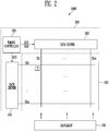
- FIG. 2 is a block diagram illustrating a display device that can be produced by the method according to some exemplary embodiments.
- the display device 1000 may include a display panel 100, and a driving circuit 200.
- the display panel 100 may be a liquid crystal panel, and the display device 1000 may further include a backlight 150.
- a plurality of gate lines GL1 to GLn extending in a first direction may be included in the display panel 100.
- a plurality of data lines DL1 to DLm extending in a second direction, e.g., a vertical direction (column direction), intersecting the first direction may be disposed in the display panel 100.
- each pixel P of the display panel 100 may include a thin film transistor, a liquid crystal capacitor, and a storage capacitor.
- each pixel P may display light of one of red, green, and blue.
- the backlight 150 functions to supply light to the display panel 100.
- a cold cathode fluorescent lamp (CCFL), an external electrode fluorescent lamp (EEFL), a light emitting diode (LED), etc. may be used as a light source of the backlight 150.
- the driving circuit 200 may include a timing controller 220, a gate driver 240, and a data driver 260.
- the timing controller 220 may receive image data from a source, e.g., an external graphic source, such as a television system or a video card, and receive a control signal including a vertical synchronization signal, a horizontal synchronization signal, a main clock signal, a data enable signal, and/or the like.
- the timing controller 220 may generate a data control signal DCS for controlling the data driver 260 in response to the input control signal.
- the data control signal DCS may include a source start pulse (SSP), a source sampling clock (SSC), a source output enable (SOE), a polarity (POL), and/or the like signals.
- the timing controller 220 may receive image data, align the received image data, and transfer the aligned image data RGB to the data driver 260.
- the timing controller 220 may generate a gate control signal GCS for controlling the gate driver 240 in response to the control signal.
- the data driver 260 may supply a data voltage to the data lines DL1 to DLm in response to the data control signal DCS and the image data RGB.
- the gate driver 240 may select (e.g., sequentially select) the gate lines GL1 to GLn in response to the gate control signal GCS supplied from the timing controller 220, and output a turn-on voltage to the selected gate line among the gate lines GL1 to GLn.
- a thin film transistor connected to the corresponding gate line may be turned on by the turn-on voltage.
- FIG. 3 is a sectional view schematically illustrating the display device of FIG. 2
- the display device 1000 may include a display panel 100 and polarizing layers 80 and 90.
- FIG. 3 illustrates a portion of a section of the display device 1000.
- the display panel 100 may include a first substrate 10, a second substrate 70, and a liquid crystal layer 44 between the first substrate 10 and the second substrate 70.
- the display panel 100 may include a first substrate 10 provided with a thin film transistor TR and a pixel electrode 42, a second substrate 70 provided with a common electrode 46 and a color filter 60, and a liquid crystal layer 44 disposed between the first substrate 10 and the second substrate 70.
- a gate electrode 22 may be formed on the first substrate 10, and a gate insulating layer 24 may be formed over the gate electrode 22.
- a semiconductor layer 26 may be formed on the gate insulating layer 24 corresponding to the gate electrode 22, and a source electrode 28A and a drain electrode 28B, which are spaced apart from each other, may be formed on the semiconductor layer 26.
- the gate electrode 22, the semiconductor layer 26, the source electrode 28A, and the drain electrode 28B may constitute a thin film transistor (TFT) TR.
- TFT thin film transistor
- the thin film transistor TR having a bottom-gate structure is illustrated in FIG. 3 , exemplary embodiments are not limited thereto.
- the thin film transistor TR may be formed in a top-gate structure, a dual-gate structure, etc.
- a protective layer 30 is formed over the thin film transistor TR, and a pixel electrode 42 connected to the drain electrode 28B may be formed on the protective layer 30.
- a common electrode 46 may be formed above the pixel electrode 42.
- the liquid crystal layer 44 including a plurality of liquid crystal molecules 45 may be provided between the pixel electrode 42 and the common electrode 46.
- a color filter 60 may be formed on the common electrode 46.
- a black matrix 62 may be provided in a recess of the color filter 60.
- a protective layer (overcoat layer) may be further disposed between the common electrode 46 and the color filter 60.
- a data signal is applied to the pixel electrode 42 through the thin film transistor TR so that an electric field is generated between the pixel electrode 42 and the common electrode 46.
- the plurality of liquid crystal molecules 45 of the liquid crystal layer 44 are rearranged along the electric field so that a corresponding pixel P can display a grayscale corresponding to the data signal.
- the thin film transistor TR, the pixel electrode 42, and the common electrode 46 may respectively extend through conductive lines, and be electrically connected respectively to side conductive patterns formed at a side of the display panel 100.
- the thin film transistor TR, the pixel electrode 42, and the common electrode 46 may be provided on the first substrate 10, and the color filter 60 may be provided on the second substrate 70.
- the liquid crystal layer 44 may be disposed between the first substrate 10 and the second substrate 70.
- the liquid crystal molecules 45 may be arranged in a horizontal direction by the electric field formed between the pixel electrode 42 and the common electrode 46 (e.g., an in-plane switching (IPS) mode, a plane to line switching (PLS) mode, a fringe field switching (FFS) mode, etc.).
- IPS in-plane switching
- PLS plane to line switching
- FFS fringe field switching
- the thin film transistor TR, the pixel electrode 42, the common electrode 46, and the color filter 60 may be provided on the first substrate 10 (e.g., a color filter on array (COA) structure).
- the liquid crystal layer 44 and the second substrate 70 may be sequentially disposed on the color filter 60.
- the polarizing layers 80 and 90 may be respectively disposed at the top and bottom of the display panel 100.
- a first polarizing layer 80 may be disposed on the top of the color filter 60
- a second polarizing layer 90 may be disposed under the bottom of the first substrate 10.
- the first and second polarizing layers 80 and 90 may be provided in the form of a polarizing film.
- the polarization axes of the first and second polarizing layers 80 and 90 may be orthogonal to each other.
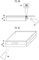
- FIGS. 4A to 4G are views of a display device at various stages of manufacture according to some exemplary embodiments.
- FIG. 5 is a flowchart illustrating an example of the method shown in FIG. 1 according to some exemplary embodiments.
- the method of manufacturing the display device 1000 may include disposing a polarizing layer 80A (a preliminary polarizing layer) on the top of a display panel 100 (S100), cutting the polarizing layer 80A (S220), cleaning a side of the display panel 100 using atmospheric pressure plasma (S240), applying a conductive paste CPA onto the side of the display panel 100 (S300), hardening the conductive paste CPA (S420 and S440), patterning the conductive paste CPA using a patterning laser beam (S460), and electrically connecting a driving circuit 200 to a side conductive pattern CP (S500).
- a polarizing layer 80A a preliminary polarizing layer
- a polarizing layer 80A may be disposed on the top of a display panel 100 in which a thin film transistor TR, a pixel electrode 42, a common electrode 46, a liquid crystal layer 44, and a color filter 60 are formed (S100).
- the display panel 100 may include a first substrate 10, a second substrate 70, and a liquid crystal layer 44 between the first substrate 10 and the second substrate 70.
- the thin film transistor TR and the pixel electrode 42 may be provided on the first substrate 10, and the common electrode 46 and the color filter 60 may be provided on the second substrate 70.
- the thin film transistor TR, the pixel electrode 42, and the common electrode 46 may be provided on the first substrate 10, and the color filter 60 may be provided on the second substrate 70.
- the thin film transistor TR, the pixel electrode 42, the common electrode 46, and the color filter 60 may be provided on the first substrate 10.
- the liquid crystal panel 50 may include the first substrate 10, the thin film transistor TR, the pixel electrode 42, the common electrode 46, and the liquid crystal layer 44.
- the color filter 60 may further include components of the second substrate 70 provided on the color filter 60.
- the display panel 100 is in a state in which it is cut by scribing a mother substrate using e.g. a diamond cutter, a laser cutter, or the like. Therefore, the flatness of a side of the display panel 100 may be low and impurities may exist.
- the polarizing layer 80A may be attached onto the color filter 60.
- FIG. 4A illustrates that the polarizing layer 80A is disposed on only the color filter 60, exemplary embodiments are not limited thereto.
- the polarizing layer 80A may be disposed on the top and under the bottom of the display panel 100 such that their polarization axes are orthogonal to each other.
- the process of disposing the polarizing layer 80A may include a cleaning process of removing an alien substance of the display panel 100, an attachment process of attaching the polarizing layer 80A while separating a protective film after the display panel 100 and the polarizing layer 80A are aligned, and an autoclave process for removing bubbles between the polarizing layer 80A and the display panel 100 and enhancing adhesion between the polarizing layer 80A and the display panel 100.
- a planar area of the polarizing layer 80A is larger than that of the display panel 100 so as to enhance adhesion between the polarizing layer 80A and the display panel 100.
- the polarizing layer 80A is cut such that a side of the polarizing layer 80A corresponds to that of the display panel 100 (S200).
- the side of the display panel 100 is polished at the same time when the polarizing layer 80A is cut by a cutting laser beam from a laser cutter 300 (S200).
- residues and impurities that are generated by the cutting and polishing may be inhaled via a suction unit 400 (S220).
- the cutting laser beam may be output from a predetermined laser cutter 300.
- the cutting laser beam may be a femto-second laser beam, and may be implemented using a gas laser, such as a helium-neon (He-Ne) laser or a carbon dioxide (CO 2 ) laser in an infrared waveform band.
- a gas laser such as a helium-neon (He-Ne) laser or a carbon dioxide (CO 2 ) laser in an infrared waveform band.
- the cutting laser beam may be accurately irradiated onto the polarizing layer 80A and the side of the display panel 100 corresponding thereto.
- the side of the polarizing layer 80A and the side of the display panel 100 that are cut by the cutting laser beam are planarized. That is, a step difference between the side of the polarizing layer 80A and the side of the display panel 100 is removed.
- the step difference between the side of the polarizing layer 80A and the side of the display panel 100 may be 100 ⁇ m or less.
- the step difference between the side of the polarizing layer 80A and the side of the display panel 100 is 0, i.e., there is no step difference.
- a side of the substrate is planarized using an edge grinding technique.
- edge grounding technique much facility cost is required to perform the edge grounding technique, it is difficult to form a step difference within 200 ⁇ m, and the panel damage rate caused by a physical impact is relatively high.
- a step difference between the side of the polarizing layer 80A and the side of the display panel 100 is decreased to 100 ⁇ m or less at low cost, and the strength of an edge portion can be enhanced.
- the step difference between the side of the polarizing layer 80A and the side of the display panel 100 may be 50 ⁇ m or less.
- Residue and alien substances such as fumes may be generated by the cutting of the polarizing layer 80A and the polishing of the display panel 100, and the side of the display panel 100 may be contaminated. Accordingly, a suction unit 400 may be provided, and the contamination can be prevented by inhaling the fumes.
- FIG. 4B illustrates that the laser cutting process is performed on only one side of the display panel 100
- exemplary embodiments are not limited thereto.
- the laser cutting and polishing process may be performed on other sides of the display panel 100.
- the side of the display panel 100 may be cleaned by atmospheric pressure plasma using a plasma cleaning unit 500 (S240).
- a contaminant such as an organic material, which exists at the side through plasma cleaning, may be removed once more.
- a hydrophilic property is provided to the surface of the display panel 100 such that a surface contact angle is lowered. Accordingly, adhesion between a conductive paste and the side of the display panel 100 can be enhanced.
- a conductive paste CPA is applied onto the side of the display panel 100 on which the plasma cleaning has been performed (S300).
- the conductive paste CPA may be integrally formed in a preset (or predetermined) application region of the display panel 100 through a printing technique.
- the conductive paste CPA may be integrally formed in the application region through a spraying technique.
- the application region may include a portion of one side of the display panel 100.
- the application region of the one side of the display panel 100 may be a region including a portion of the liquid crystal panel 50 and a portion of the color filter 60.
- the application region of the one side of the display panel 100 may include only a portion of the liquid crystal panel 50.
- the application region may be formed at a plurality of sides of the display panel 100.
- the application region may be formed to be in contact with a plurality of connecting lines CL formed in the liquid crystal panel 50.
- Each of the connecting lines CL may be connected to at least one of the thin film transistor TR, the pixel electrode 42, the common electrode 46, and the color filter 60.
- the conductive paste CPA may include a metallic material having high electrical conductivity.
- the conductive paste CPA may include at least one selected from silver (Ag), copper (Cu), gold (Au), and aluminum (Al).
- the conductive paste CPA may be pre-hardened by hot air (S420).
- a heating unit may supply hot air of about 90 °C to the conductive paste CPA to maintain the shape of the conductive paste CPA.
- the conductive paste CPA formed at the side of the display panel 100 may flow down due to gravity, but the pre-hardening process can prevent the shape of the conductive paste CPA from being changed.
- this is merely illustrative, and the pre-hardening process may be omitted to reduce process time.
- the pre-hardened conductive paste CPA may be hardened by irradiating a hardening laser beam onto the pre-hardened conductive paste CPA (S440).
- the hardening laser beam is a square-wave laser beam having an infrared waveform, which forms high temperature of 200 °C or more.
- the hardening laser beam locally supplies high-temperature heat so that a portion, except the application region, can be prevented from being heated. Thus, another portion of the display panel including liquid crystals, etc. can be prevented from being damaged.
- a volatile material in the conductive paste CPA is evaporated, and only a pure conductive material (e.g., silver (Ag)) may remain. Further, the conductive material may be firmly fixed to the side of the display panel 100 through the hardening process, and the surface hardness of the conductive material may be reinforced. However, this is merely illustrative, and the hardening process of the conductive paste CPA may be performed after the patterning process so as to reduce process time.
- the conductive paste CPA is patterned by a patterning laser beam (S460).
- the patterning laser beam may have a wavelength in an infrared area, and etch the hardened conductive paste CPA.
- the patterning laser beam may perform patterning even at a distance of about 20 ⁇ m or less between side conductive patterns CP.
- a plurality of side conductive patterns CP may be formed through laser patterning.
- the side conductive patterns CP may be electrically connected to the connecting lines CL, respectively.
- one side portion of the connecting line CL is connected to the side conductive pattern CP so that the connecting line CL and the side conductive pattern CP can be electrically connected to each other.
- the distance D1 between the side conductive patterns CP may be set to about 30 ⁇ m or less.
- the laser patterning process may be performed such that the distance D1 between the side conductive patterns CP is about 150 ⁇ m, corresponding to full HD resolution, or may be performed such that the distance D1 between the side conductive patterns CP is about 50 ⁇ m, corresponding to UHD or 4k UHD resolution.
- the laser patterning process may be performed such that the distance D1 between the side conductive patterns CP is about 25 ⁇ m, corresponding to 8k UHD or more resolution. That is, the distance between the side conductive patterns CP can be relatively easily controlled corresponding to the distance between pixels (or connecting lines CL) formed in the display panel 100, the number of pixels (or connecting lines CL) formed in the display panel 100, etc.
- the lateral width D2 of each of the side conductive patterns CP may be within a range of about 2 ⁇ m to 4 ⁇ m.
- the conductive paste may be removed by the laser patterning in the application region except the side conductive patterns CP.
- boundaries of the side conductive patterns CP having a very dense distance through the laser patterning can be clearly distinguished.
- the laser patterning for forming the side conductive patterns CP cost for a jig is not required, the conductive patterns can be accurately machined, and production cost can be considerably reduced. Further, the laser patterning can be effectively used in manufacturing of display devices having various high resolutions, such as FHD, UHD, 4k UHD, and 8k UHD.
- a color difference may be shown between a portion at which the conductive paste CPA is removed by the laser patterning and a portion at which the conductive paste is not attached.
- the portion at which the conductive paste CPA is removed by the laser patterning is not conducted.
- an anisotropic conductive film ACF may be attached to the side conductive patterns CP, and a driving circuit 200 and a printed circuit board (PCB) may be electrically connected to the side conductive patterns CP (e.g., an outer lead bonding (OLB) process) (S500).
- a driving circuit 200 and a printed circuit board (PCB) may be electrically connected to the side conductive patterns CP (e.g., an outer lead bonding (OLB) process) (S500).
- OLB outer lead bonding
- a plurality of anisotropic conductive films ACF may be attached to one side of the display panel 100 at a predetermined distance from one another. Therefore, the display panel 100 may be electrically connected to the driving circuit 200 through side bonding.
- the side conductive patterns CP may be attached to a first portion of each of the anisotropic conductive films ACF.
- a conductive film CF including conductive lines and the driving circuit 200 may be attached to a second portion of each of the anisotropic conductive films ACF.
- the driving circuit 200 may include at least one of the timing controller 220, the gate driver 240, and the data driver 260.
- the timing controller 220, the gate driver 240, and the data driver 260 may be implemented with a driving integrated circuit (IC) chip, an IC, etc. This, however, is merely illustrative, and the form and configuration of the driving circuit 200 are not limited thereto.
- at least one of the timing controller 220, the gate driver 240, and the data driver 260 may be integrated in or on the display panel 100.
- the driving circuit 200 may be electrically connected to an external controller, a processor, etc., through a PCB.
- a step difference between the display panel 100 and the polarizing layer 80 is removed by the laser cutting and polishing so that the width of a bezel for the OLB process can be considerably reduced.
- the side conductive patterns CP are accurately formed by the ultra-fine laser patterning so that a large-sized display device having ultra-high resolution of UHD or more can be implemented.
- FIG. 6 is a flowchart illustrating an example of the method shown in FIG. 1 according to some exemplary embodiments.
- FIG. 6 The method of FIG. 6 is identical to the method according to FIG. 5 , except the order of a process of hardening a conductive paste. Therefore, identical or corresponding components and processes are designated by like reference numerals, and their overlapping descriptions will be omitted.
- the method of manufacturing the display device 1000 may include disposing a polarizing layer 80 on the top of a display panel 100 (S100), cutting the polarizing layer 80 (S220), cleaning a side of the display panel 100 using atmospheric pressure plasma (S240), applying a conductive paste CPA onto the side of the display panel 100 (S300), pre-hardening the conductive paste CPA (S420), patterning the conductive paste CPA using a patterning laser beam (S450), and hardening the patterned conductive paste CPA using a hardening laser beam (S470).
- the steps S100, S220, S240, S300, and S420 have been described with reference to FIGS. 3 to 4D , and therefore, their overlapping descriptions will be omitted.
- a pre-hardened conductive paste CPA may be patterned into side conductive patterns CP by a patterning laser beam (S450).
- the pre-hardened conductive paste CPA is in a state in which its hardness is weak, and therefore, a laser machining number may decrease.
- laser patterning may be performed eight times or more so as to pattern the completely hardened conductive paste CPA.
- the side conductive patterns CP may be formed by performing only two-time or three-time laser patterning on the pre-hardened conductive paste CPA. Accordingly, a laser patterning number decreases, and thus, manufacturing time and manufacturing cost can be reduced.
- the side conductive patterns CP may be hardened by a hardening laser beam (S470).
- FIG. 7 is a view briefly illustrating a facility for performing the method shown in FIG. 1 according to some exemplary embodiments.
- the method may be performed through an in-line process. That is, processes including a process of patterning the side conductive patterns CP, an OLB process, and an unloading process from a process of loading the display panel 100 may be automatically performed in a lump, e.g., in an assembly line fashion.
- the facility for manufacturing the display device 1000 may include a laser cutting unit 300, a plasma cleaning unit 500, a conductive paste printing unit 600, an air heating unit 700, a laser hardening unit 800, and a laser patterning unit 900. Also, the facility may further include an autoclave for combining the polarizing layer 80 and the display panel 100 together.
- the display panel 100 may be conveyed in a direction parallel to the top of the display panel 100 along a conveyor.
- attaching a polarizing layer 80A to the display panel 100 S100
- cutting the polarizing layer 80A S220
- cleaning a side of the display panel 100 S240
- applying a conductive paste CPA S300
- pre-hardening the conductive paste CPA S420
- hardening the conductive paste CPA S440
- patterning the conductive paste CPA to side conductive patterns CP S460
- FIGS. 8A to 8C are views illustrating a display device that can be produced by the method according to some exemplary embodiments.
- a plurality of display devices 1001 to 1004 may be coupled to display an image.
- the display devices 1001 to 1004 may be connected to implement a public information display (PID) having an outdoor display structure, etc.
- Image quality may be degraded due to a bezel between the display devices 1001 to 1004.
- the bezel is viewed, and therefore, it may interfere with video viewing.
- a conductive film CF including a driving IC, etc. is bonded to side conductive patterns so that the width of the bezel can be remarkably decreased.
- the width of chassis CH1 and CH2 for covering the display devices 1001 to 1004 and preventing light leakage can be decreased.
- the width of a connecting part for connecting two adjacent display devices among the display devices 1001 to 1004 may be decreased to less than about 1 mm, and the shortest distance between pixel regions of two actually adjacent display devices may be decreased to less than about 1.5 mm.
- the bezel between the display devices 1001 to 1004 is not viewed in the combined display structure in which the plurality of display devices 1001 to 1004 are connected to display one image.
- the PID can display an image having ultra-high resolution of UHD or more, using ultra-fine side conductive patterns.
- the chassis CH1 and CH2 may cover a portion (e.g., bezel portion) of the top of each of the display devices 1001 to 1004.
- a portion of the chassis CH1 and CH2 may overlap with a sealing part SEAL of each of the display devices 1001 to 1004.
- the chassis CH1 and CH2 do not cover the bezel between the display devices 1001 to 1004, and the bezel between the display devices 1001 to 1004 may be covered using a material such as resin RES.
- a material such as resin RES.
- the resin RES may connect the chassis CH1 and CH2 and the display devices 1001 to 1004 or connect the chassis CH1 and CH2 and each of the display devices 1001 to 1004, as well as cover the bezel. Accordingly, the width of the bezel between the display devices 1001 to 1004 is decreased, and the connecting part and bezel between the display devices 1001 to 1004 are not viewed by a user.
- FIG. 9 is a flowchart illustrating an example of a method of manufacturing a display device according to some exemplary embodiments.
- the method of FIG. 9 is a method obtained by omitting some processes of the method according to FIG. 5 or changing the order of some processes of the method according to FIG. 5 . Therefore, identical or corresponding components and processes are designated by like reference numerals, and their overlapping descriptions will be omitted.
- the method may include cleaning a side of a display panel using atmospheric pressure plasma (S110), applying a conductive paste onto the side of the display panel (S210), hardening the conductive paste using a laser beam (S310), patterning the hardened conductive paste using a patterning laser beam (S410), and disposing a polarizing layer on the display panel (510).
- the polarizing layer may be disposed after side conductive patterns are formed. Therefore, a process of cutting the polarizing layer may be omitted. In addition a pre-hardening process is omitted. Accordingly, manufacturing time and manufacturing cost can be considerably reduced.
- Display devices that can be produced by the method according to exemplary embodiments can be applied to televisions, computer monitors, notebook computers, digital cameras, mobile phones, smart pads, personal digital assistants, personal media players, MP3 players, navigation systems, camcorders, potable game consoles, and the like. Also, they can be applied to outdoor advertising boards, large-sized displays, electronic displays, public information displays, and the like.
- a step difference between a display panel and a polarizing layer is removed through laser cutting and polishing so that the width of a bezel for an OLB process can be considerably decreased.
- side conductive patterns can be accurately formed through ultra-fine laser patterning so that a large-sized display device having ultra-high resolution of UHD or more can be implemented.
Landscapes
- Physics & Mathematics (AREA)
- Nonlinear Science (AREA)
- Optics & Photonics (AREA)
- General Physics & Mathematics (AREA)
- Crystallography & Structural Chemistry (AREA)
- Chemical & Material Sciences (AREA)
- Mathematical Physics (AREA)
- Engineering & Computer Science (AREA)
- Manufacturing & Machinery (AREA)
- Mechanical Engineering (AREA)
- Plasma & Fusion (AREA)
- Microelectronics & Electronic Packaging (AREA)
- Devices For Indicating Variable Information By Combining Individual Elements (AREA)
- Liquid Crystal (AREA)
Description
- Exemplary embodiments generally relate to a method of manufacturing a display device, and more particularly, a liquid crystal display device.
- Display fields have been rapidly developed. In response, liquid crystal display (LCD) devices, plasma display panel (PDP) devices, electroluminescence display (ELD) devices, field emission display (FED) devices, and the like, are being developed as flat panel display devices having advantages of thinness, lightweight, and low power consumption. LCD devices are actively used in various fields, such as notebook computers, monitors, televisions, large-sized displays, and the like, due to excellent moving picture display and a high contrast ratio.
- A plurality of display panels may be connected to display an image in an outdoor display, an electronic display, etc. However, a connecting portion between the display panels can be viewed due to a bezel between the display panels, and therefore, the connecting portion may interfere with video viewing. Accordingly, interest in minimizing a bezel between display panels is growing, as well as interest in realizing image display with ultra-high resolution.
- The above information disclosed in this section is only for understanding the background of the inventive concepts, and, therefore, may contain information that does not form prior art.
-
US 2018/173042 A1 discloses a method of manufacturing a display device, the method comprising the subsequent steps of providing a display panel comprising a thin film transistor and a pixel electrode, and applying a conductive paste onto the side of the display panel and patterning the conductive paste using a patterning laser. A laser is used to cut the side edges of the panel substrates so that they are coplanar and so that the conductive paste for electrical contact can then be applied to the planar side surface. -
KR 2016 0028550 A - Some exemplary embodiments provide a method of manufacturing a display device, in which ultra-fine conductive patterns are formed at a side surface of the display device.
- Some exemplary embodiments provide a method of manufacturing a display device that has a side at which a
step difference between a display panel and a polarizing layer is removed (or at least reduced), and includes the display panel having a side at which ultra-fine conductive patterns are formed. - Additional aspects will be set forth in the detailed description which follows, and, in part, will be apparent from the disclosure, or may be learned by practice of the inventive concepts.
- According to exemplary embodiments, a method of manufacturing a display device includes the features of appended independent claim 1.
- Preferred embodiments are defined in the appended dependent claims.
- Due to the invention the manufacturing process of producing a display device takes less time than with conventional methods.
- The foregoing general description and the following detailed description are exemplary and explanatory and are intended to provide further explanation of the claimed subject matter.
- The accompanying drawings, which are included to provide a further understanding of the inventive concepts, and are incorporated in and constitute a part of this specification, illustrate exemplary embodiments of the inventive concepts, and, together with the description, serve to explain principles of the inventive concepts.
-
FIG. 1 is a flowchart illustrating a method of manufacturing a display device according to some exemplary embodiments. -
FIG. 2 is a block diagram illustrating a display device that can be produced by a method according to some exemplary embodiments. -
FIG. 3 is a sectional view schematically illustrating the display device ofFIG. 2 . -
FIGS. 4A ,4B ,4C ,4D ,4E ,4F, and 4G are views of a display device at various stages of manufacture according to some exemplary embodiments. -
FIG. 5 is a flowchart illustrating an example of the method shown inFIG. 1 according to some exemplary embodiments. -
FIG. 6 is a flowchart illustrating an example of the method shown inFIG. 1 according to some exemplary embodiments. -
FIG. 7 is a view briefly illustrating a facility for performing the method shown inFIG. 1 according to some exemplary embodiments. -
FIGS. 8A ,8B, and 8C are views illustrating a display that can be produced by the method according to some exemplary embodiments. -
FIG. 9 is a flowchart illustrating an example of a method of manufacturing a display device according to some exemplary embodiments. - In the following description, for the purposes of explanation, numerous specific details are set forth in order to provide a thorough understanding of various exemplary embodiments. It is apparent, however, that various exemplary embodiments may be practiced without these specific details or with one or more equivalent arrangements. In other instances, well-known structures and devices are shown in block diagram form in order to avoid unnecessarily obscuring various exemplary embodiments. Further, various exemplary embodiments may be different, but do not have to be exclusive. For example, specific shapes, configurations, and characteristics of an exemplary embodiment may be used or implemented in another exemplary embodiment without departing from the inventive concepts.
- Unless otherwise specified, the illustrated exemplary embodiments are to be understood as providing exemplary features of varying detail of some exemplary embodiments. Therefore, unless otherwise specified, the features, components, modules, layers, films, panels, regions, aspects, etc. (hereinafter individually or collectively referred to as an "element" or "elements"), of the various illustrations may be otherwise combined, separated, interchanged, and/or rearranged without departing from the inventive concepts.
- The use of cross-hatching and/or shading in the accompanying drawings is generally provided to clarify boundaries between adjacent elements. As such, neither the presence nor the absence of cross-hatching or shading conveys or indicates any preference or requirement for particular materials, material properties, dimensions, proportions, commonalities between illustrated elements, and/or any other characteristic, attribute, property, etc., of the elements, unless specified. Further, in the accompanying drawings, the size and relative sizes of elements may be exaggerated for clarity and/or descriptive purposes. As such, the sizes and relative sizes of the respective elements are not necessarily limited to the sizes and relative sizes shown in the drawings. When an exemplary embodiment may be implemented differently, a specific process order may be performed differently from the described order. For example, two consecutively described processes may be performed substantially at the same time or performed in an order opposite to the described order. Also, like reference numerals denote like elements.
- When an element is referred to as being "on," "connected to," or "coupled to" another element, it may be directly on, connected to, or coupled to the other element or intervening elements may be present. When, however, an element is referred to as being "directly on," "directly connected to," or "directly coupled to" another element, there are no intervening elements present. Other terms and/or phrases used to describe a relationship between elements should be interpreted in a like fashion, e.g., "between" versus "directly between," "adjacent" versus "directly adjacent," "on" versus "directly on," etc. Further, the term "connected" may refer to physical, electrical, and/or fluid connection. For the purposes of this disclosure, "at least one of X, Y, and Z" and "at least one selected from the group consisting of X, Y, and Z" may be construed as X only, Y only, Z only, or any combination of two or more of X, Y, and Z, such as, for instance, XYZ, XYY, YZ, and ZZ. As used herein, the term "and/or" includes any and all combinations of one or more of the associated listed items.
- Although the terms "first," "second," etc. may be used herein to describe various elements, these elements should not be limited by these terms. These terms are used to distinguish one element from another element. Thus, a first element discussed below could be termed a second element without departing from the teachings of the disclosure.
- Spatially relative terms, such as "beneath," "below," "under," "lower," "above," "upper," "over," "higher," "side" (e.g., as in "sidewall"), and the like, may be used herein for descriptive purposes, and, thereby, to describe one element's relationship to another element(s) as illustrated in the drawings. Spatially relative terms are intended to encompass different orientations of an apparatus in use, operation, and/or manufacture in addition to the orientation depicted in the drawings. For example, if the apparatus in the drawings is turned over, elements described as "below" or "beneath" other elements or features would then be oriented "above" the other elements or features. Thus, the exemplary term "below" can encompass both an orientation of above and below. Furthermore, the apparatus may be otherwise oriented (e.g., rotated 90 degrees or at other orientations), and, as such, the spatially relative descriptors used herein interpreted accordingly.
- The terminology used herein is for the purpose of describing particular embodiments and is not intended to be limiting. As used herein, the singular forms, "a," "an," and "the" are intended to include the plural forms as well, unless the context clearly indicates otherwise. Moreover, the terms "comprises," "comprising," "includes," and/or "including," when used in this specification, specify the presence of stated features, integers, steps, operations, elements, components, and/or groups thereof, but do not preclude the presence or addition of one or more other features, integers, steps, operations, elements, components, and/or groups thereof. It is also noted that, as used herein, the terms "substantially," "about," and other similar terms, are used as terms of approximation and not as terms of degree, and, as such, are utilized to account for inherent deviations in measured, calculated, and/or provided values that would be recognized by one of ordinary skill in the art.
- Various exemplary embodiments are described herein with reference to cross-sectional views, isometric views, perspective views, plan views, and/or exploded illustrations that are schematic illustrations of idealized exemplary embodiments and/or intermediate structures. As such, variations from the shapes of the illustrations as a result of, for example, manufacturing techniques and/or tolerances, are to be expected. Thus, exemplary embodiments disclosed herein should not be construed as limited to the particular illustrated shapes of regions, but are to include deviations in shapes that result from, for instance, manufacturing. To this end, regions illustrated in the drawings may be schematic in nature and shapes of these regions may not reflect the actual shapes of regions of a device, and, as such, are not intended to be limiting.
- Unless otherwise defined, all terms (including technical and scientific terms) used herein have the same meaning as commonly understood by one of ordinary skill in the art to which this disclosure is a part. Terms, such as those defined in commonly used dictionaries, should be interpreted as having a meaning that is consistent with their meaning in the context of the relevant art and will not be interpreted in an idealized or overly formal sense, unless expressly so defined herein.
- As customary in the field, some exemplary embodiments are described and illustrated in the accompanying drawings in terms of functional blocks, units, and/or modules. Those skilled in the art will appreciate that these blocks, units, and/or modules are physically implemented by electronic (or optical) circuits, such as logic circuits, discrete components, microprocessors, hard-wired circuits, memory elements, wiring connections, and the like, which may be formed using semiconductor-based fabrication techniques or other manufacturing technologies. In the case of the blocks, units, and/or modules being implemented by microprocessors or other similar hardware, they may be programmed and controlled using software (e.g., microcode) to perform various functions discussed herein and may optionally be driven by firmware and/or software. It is also contemplated that each block, unit, and/or module may be implemented by dedicated hardware, or as a combination of dedicated hardware to perform some functions and a processor (e.g., one or more programmed microprocessors and associated circuitry) to perform other functions. Also, each block, unit, and/or module of some exemplary embodiments may be physically separated into two or more interacting and discrete blocks, units, and/or modules without departing from the inventive concepts. Further, the blocks, units, and/or modules of some exemplary embodiments may be physically combined into more complex blocks, units, and/or modules without departing from the inventive concepts.
- Hereinafter, various exemplary embodiments will be explained in detail with reference to the accompanying drawings. Throughout the drawings and description, the same or similar reference numerals are given to the same or similar elements, and their overlapping descriptions will be omitted.
-
FIG. 1 is a flowchart illustrating a method of manufacturing a display device according to some exemplary embodiments. - Referring to
FIG. 1 , a method of manufacturing a display device may include: - disposing a polarizing layer on a top of a display panel (S100); cutting the polarizing layer using a cutting laser beam (S200); applying a conductive paste onto a side of the display panel (S300);
- patterning the conductive paste using a patterning laser beam (S400), and electrically connecting a driving circuit to a side conductive pattern (S500).
- In some exemplary embodiments, the display device may be a liquid crystal display (LCD) device. Hereinafter, a case where the display device is an LCD device will be described. However, this is merely illustrative, and the display device is not limited thereto. For example, the display device may be a plasma display panel (PDP), an organic light emitting diode (OLED) display device, a field effect display (FED) device, an electrophoretic display device, or the like.
- The display device manufactured as described above may have a side from which a step difference between a polarizing layer and a display panel is removed. In addition, side conductive patterns connected to an internal circuit of the display panel by a laser (e.g., high accuracy laser) technique may be formed at the side from which the step difference is removed. Accordingly, a driving circuit for driving the display device can be electrically connected to the display panel through side bonding of the display panel.
- In a conventional display device, an electrode extends on a top of a substrate in which thin film transistors are formed, an anisotropic conductive film or the like is attached onto the electrode, and a driving chip, a printed circuit board (PCB), or the like is attached to the anisotropic conductive film in a chip on film (COF) manner. Accordingly, a side step difference occurs between a polarizing layer and a display panel (e.g., substrate including a thin film transistor, etc.), and a bezel is formed. In addition, light leakage may be viewed due to the step difference between the display panel and the polarizing layer. To prevent the light leakage from being viewed, a chassis, a frame, a black matrix, and/or the like are formed at a periphery of the display panel. Accordingly, there is a limitation in reducing the width of the bezel at the periphery of the display device.
- In a display device and a method of manufacturing the same according to some exemplary embodiments, a step difference between the display panel and the polarizing layer is removed, and the display panel and the driving circuit are connected through side bonding. In this manner, a zero-bezel can be realized, and a large-sized display device having an ultra-high definition (UHD) or higher resolution can be implemented through ultra-fine laser patterning.
-
FIG. 2 is a block diagram illustrating a display device that can be produced by the method according to some exemplary embodiments. - Referring to
FIG. 2 , thedisplay device 1000 may include adisplay panel 100, and adriving circuit 200. Thedisplay panel 100 may be a liquid crystal panel, and thedisplay device 1000 may further include abacklight 150. - A plurality of gate lines GL1 to GLn extending in a first direction, e.g., a horizontal direction (row direction), may be included in the
display panel 100. A plurality of data lines DL1 to DLm extending in a second direction, e.g., a vertical direction (column direction), intersecting the first direction may be disposed in thedisplay panel 100. - The gate lines GL1 to GLn and the data lines DL1 to DLm, which intersect each other, may define pixels P. Although not shown, each pixel P of the
display panel 100 may include a thin film transistor, a liquid crystal capacitor, and a storage capacitor. In some exemplary embodiments, each pixel P may display light of one of red, green, and blue. - The
backlight 150 functions to supply light to thedisplay panel 100. A cold cathode fluorescent lamp (CCFL), an external electrode fluorescent lamp (EEFL), a light emitting diode (LED), etc. may be used as a light source of thebacklight 150. - The driving
circuit 200 may include atiming controller 220, agate driver 240, and adata driver 260. - The
timing controller 220 may receive image data from a source, e.g., an external graphic source, such as a television system or a video card, and receive a control signal including a vertical synchronization signal, a horizontal synchronization signal, a main clock signal, a data enable signal, and/or the like. Thetiming controller 220 may generate a data control signal DCS for controlling thedata driver 260 in response to the input control signal. The data control signal DCS may include a source start pulse (SSP), a source sampling clock (SSC), a source output enable (SOE), a polarity (POL), and/or the like signals. Also, thetiming controller 220 may receive image data, align the received image data, and transfer the aligned image data RGB to thedata driver 260. Thetiming controller 220 may generate a gate control signal GCS for controlling thegate driver 240 in response to the control signal. - The
data driver 260 may supply a data voltage to the data lines DL1 to DLm in response to the data control signal DCS and the image data RGB. - The
gate driver 240 may select (e.g., sequentially select) the gate lines GL1 to GLn in response to the gate control signal GCS supplied from thetiming controller 220, and output a turn-on voltage to the selected gate line among the gate lines GL1 to GLn. A thin film transistor connected to the corresponding gate line may be turned on by the turn-on voltage. -
FIG. 3 is a sectional view schematically illustrating the display device ofFIG. 2 - Referring to
FIG. 3 , thedisplay device 1000 may include adisplay panel 100 andpolarizing layers FIG. 3 illustrates a portion of a section of thedisplay device 1000. - The
display panel 100 may include afirst substrate 10, asecond substrate 70, and a liquid crystal layer 44 between thefirst substrate 10 and thesecond substrate 70. - In some exemplary embodiments, the
display panel 100 may include afirst substrate 10 provided with a thin film transistor TR and apixel electrode 42, asecond substrate 70 provided with acommon electrode 46 and acolor filter 60, and a liquid crystal layer 44 disposed between thefirst substrate 10 and thesecond substrate 70. - A
gate electrode 22 may be formed on thefirst substrate 10, and agate insulating layer 24 may be formed over thegate electrode 22. Asemiconductor layer 26 may be formed on thegate insulating layer 24 corresponding to thegate electrode 22, and asource electrode 28A and adrain electrode 28B, which are spaced apart from each other, may be formed on thesemiconductor layer 26. - The
gate electrode 22, thesemiconductor layer 26, thesource electrode 28A, and thedrain electrode 28B may constitute a thin film transistor (TFT) TR. Although the thin film transistor TR having a bottom-gate structure is illustrated inFIG. 3 , exemplary embodiments are not limited thereto. For example, the thin film transistor TR may be formed in a top-gate structure, a dual-gate structure, etc. - A
protective layer 30 is formed over the thin film transistor TR, and apixel electrode 42 connected to thedrain electrode 28B may be formed on theprotective layer 30. - A
common electrode 46 may be formed above thepixel electrode 42. In some exemplary embodiments, the liquid crystal layer 44 including a plurality ofliquid crystal molecules 45 may be provided between thepixel electrode 42 and thecommon electrode 46. - A
color filter 60 may be formed on thecommon electrode 46. In some exemplary embodiments, ablack matrix 62 may be provided in a recess of thecolor filter 60. In some exemplary embodiments, a protective layer (overcoat layer) may be further disposed between thecommon electrode 46 and thecolor filter 60. - When the thin film transistor TR is turned on according to a gate signal applied to the
gate electrode 22, a data signal is applied to thepixel electrode 42 through the thin film transistor TR so that an electric field is generated between thepixel electrode 42 and thecommon electrode 46. The plurality ofliquid crystal molecules 45 of the liquid crystal layer 44 are rearranged along the electric field so that a corresponding pixel P can display a grayscale corresponding to the data signal. - The thin film transistor TR, the
pixel electrode 42, and thecommon electrode 46 may respectively extend through conductive lines, and be electrically connected respectively to side conductive patterns formed at a side of thedisplay panel 100. - The thin film transistor TR, the
pixel electrode 42, and thecommon electrode 46 may be provided on thefirst substrate 10, and thecolor filter 60 may be provided on thesecond substrate 70. The liquid crystal layer 44 may be disposed between thefirst substrate 10 and thesecond substrate 70. Theliquid crystal molecules 45 may be arranged in a horizontal direction by the electric field formed between thepixel electrode 42 and the common electrode 46 (e.g., an in-plane switching (IPS) mode, a plane to line switching (PLS) mode, a fringe field switching (FFS) mode, etc.). - The thin film transistor TR, the
pixel electrode 42, thecommon electrode 46, and thecolor filter 60 may be provided on the first substrate 10 (e.g., a color filter on array (COA) structure). The liquid crystal layer 44 and thesecond substrate 70 may be sequentially disposed on thecolor filter 60. - The
polarizing layers display panel 100. For example, a firstpolarizing layer 80 may be disposed on the top of thecolor filter 60, and a secondpolarizing layer 90 may be disposed under the bottom of thefirst substrate 10. In some exemplary embodiments, the first and secondpolarizing layers display device 1000 may have only one of the first and secondpolarizing layers - The polarization axes of the first and second
polarizing layers -
FIGS. 4A to 4G are views of a display device at various stages of manufacture according to some exemplary embodiments.FIG. 5 is a flowchart illustrating an example of the method shown inFIG. 1 according to some exemplary embodiments. - Referring to
FIGS. 1 to 5 , the method of manufacturing thedisplay device 1000 may include disposing apolarizing layer 80A (a preliminary polarizing layer) on the top of a display panel 100 (S100), cutting thepolarizing layer 80A (S220), cleaning a side of thedisplay panel 100 using atmospheric pressure plasma (S240), applying a conductive paste CPA onto the side of the display panel 100 (S300), hardening the conductive paste CPA (S420 and S440), patterning the conductive paste CPA using a patterning laser beam (S460), and electrically connecting adriving circuit 200 to a side conductive pattern CP (S500). - A
polarizing layer 80A may be disposed on the top of adisplay panel 100 in which a thin film transistor TR, apixel electrode 42, acommon electrode 46, a liquid crystal layer 44, and acolor filter 60 are formed (S100). Thedisplay panel 100 may include afirst substrate 10, asecond substrate 70, and a liquid crystal layer 44 between thefirst substrate 10 and thesecond substrate 70. - In some exemplary embodiments, the thin film transistor TR and the
pixel electrode 42 may be provided on thefirst substrate 10, and thecommon electrode 46 and thecolor filter 60 may be provided on thesecond substrate 70. In some exemplary embodiments, the thin film transistor TR, thepixel electrode 42, and thecommon electrode 46 may be provided on thefirst substrate 10, and thecolor filter 60 may be provided on thesecond substrate 70. In some exemplary embodiments, the thin film transistor TR, thepixel electrode 42, thecommon electrode 46, and thecolor filter 60 may be provided on thefirst substrate 10. - In
FIGS. 4A to 4G , for convenience of description, a case where the components included in thedisplay panel 100 are divided into aliquid crystal panel 50 and thecolor filter 60 will be described. For example, theliquid crystal panel 50 may include thefirst substrate 10, the thin film transistor TR, thepixel electrode 42, thecommon electrode 46, and the liquid crystal layer 44. In addition, thecolor filter 60 may further include components of thesecond substrate 70 provided on thecolor filter 60. - The
display panel 100 is in a state in which it is cut by scribing a mother substrate using e.g. a diamond cutter, a laser cutter, or the like. Therefore, the flatness of a side of thedisplay panel 100 may be low and impurities may exist. - The
polarizing layer 80A may be attached onto thecolor filter 60. AlthoughFIG. 4A illustrates that thepolarizing layer 80A is disposed on only thecolor filter 60, exemplary embodiments are not limited thereto. For example, thepolarizing layer 80A may be disposed on the top and under the bottom of thedisplay panel 100 such that their polarization axes are orthogonal to each other. - In some exemplary embodiments, the process of disposing the
polarizing layer 80A may include a cleaning process of removing an alien substance of thedisplay panel 100, an attachment process of attaching thepolarizing layer 80A while separating a protective film after thedisplay panel 100 and thepolarizing layer 80A are aligned, and an autoclave process for removing bubbles between thepolarizing layer 80A and thedisplay panel 100 and enhancing adhesion between thepolarizing layer 80A and thedisplay panel 100. - A planar area of the
polarizing layer 80A is larger than that of thedisplay panel 100 so as to enhance adhesion between thepolarizing layer 80A and thedisplay panel 100. - Subsequently, the
polarizing layer 80A is cut such that a side of thepolarizing layer 80A corresponds to that of the display panel 100 (S200). According to exemplary embodiments, as shown inFIG. 4B , the side of thedisplay panel 100 is polished at the same time when thepolarizing layer 80A is cut by a cutting laser beam from a laser cutter 300 (S200). Simultaneously, residues and impurities that are generated by the cutting and polishing may be inhaled via a suction unit 400 (S220). - The cutting laser beam may be output from a
predetermined laser cutter 300. For example, the cutting laser beam may be a femto-second laser beam, and may be implemented using a gas laser, such as a helium-neon (He-Ne) laser or a carbon dioxide (CO2) laser in an infrared waveform band. - The cutting laser beam may be accurately irradiated onto the
polarizing layer 80A and the side of thedisplay panel 100 corresponding thereto. The side of thepolarizing layer 80A and the side of thedisplay panel 100 that are cut by the cutting laser beam are planarized. That is, a step difference between the side of thepolarizing layer 80A and the side of thedisplay panel 100 is removed. For example, the step difference between the side of thepolarizing layer 80A and the side of thedisplay panel 100 may be 100 µm or less. For instance, the step difference between the side of thepolarizing layer 80A and the side of thedisplay panel 100 is 0, i.e., there is no step difference. - In a conventional process of cutting a substrate, a side of the substrate is planarized using an edge grinding technique. However, in the edge grounding technique, much facility cost is required to perform the edge grounding technique, it is difficult to form a step difference within 200 µm, and the panel damage rate caused by a physical impact is relatively high. However, in the cutting and polishing process (S220) using the cutting laser beam according to some exemplary embodiments, a step difference between the side of the
polarizing layer 80A and the side of thedisplay panel 100 is decreased to 100 µm or less at low cost, and the strength of an edge portion can be enhanced. For example, the step difference between the side of thepolarizing layer 80A and the side of thedisplay panel 100 may be 50 µm or less. - Residue and alien substances such as fumes may be generated by the cutting of the
polarizing layer 80A and the polishing of thedisplay panel 100, and the side of thedisplay panel 100 may be contaminated. Accordingly, asuction unit 400 may be provided, and the contamination can be prevented by inhaling the fumes. - Although
FIG. 4B illustrates that the laser cutting process is performed on only one side of thedisplay panel 100, exemplary embodiments are not limited thereto. For example, the laser cutting and polishing process may be performed on other sides of thedisplay panel 100. - As shown in
FIG. 4C , the side of thedisplay panel 100 may be cleaned by atmospheric pressure plasma using a plasma cleaning unit 500 (S240). A contaminant such as an organic material, which exists at the side through plasma cleaning, may be removed once more. In addition, a hydrophilic property is provided to the surface of thedisplay panel 100 such that a surface contact angle is lowered. Accordingly, adhesion between a conductive paste and the side of thedisplay panel 100 can be enhanced. - As shown in
FIG. 4D , a conductive paste CPA is applied onto the side of thedisplay panel 100 on which the plasma cleaning has been performed (S300). In some exemplary embodiments, the conductive paste CPA may be integrally formed in a preset (or predetermined) application region of thedisplay panel 100 through a printing technique. Alternatively (or additionally), the conductive paste CPA may be integrally formed in the application region through a spraying technique. - In some exemplary embodiments, the application region may include a portion of one side of the
display panel 100. For example, the application region of the one side of thedisplay panel 100 may be a region including a portion of theliquid crystal panel 50 and a portion of thecolor filter 60. Alternatively, the application region of the one side of thedisplay panel 100 may include only a portion of theliquid crystal panel 50. - Also, as shown in
FIG. 4D , the application region may be formed at a plurality of sides of thedisplay panel 100. - The application region may be formed to be in contact with a plurality of connecting lines CL formed in the
liquid crystal panel 50. Each of the connecting lines CL may be connected to at least one of the thin film transistor TR, thepixel electrode 42, thecommon electrode 46, and thecolor filter 60. - The conductive paste CPA may include a metallic material having high electrical conductivity. In some exemplary embodiments, the conductive paste CPA may include at least one selected from silver (Ag), copper (Cu), gold (Au), and aluminum (Al).
- In some exemplary embodiments, the conductive paste CPA may be pre-hardened by hot air (S420). For example, a heating unit may supply hot air of about 90 °C to the conductive paste CPA to maintain the shape of the conductive paste CPA. For instance, the conductive paste CPA formed at the side of the
display panel 100 may flow down due to gravity, but the pre-hardening process can prevent the shape of the conductive paste CPA from being changed. However, this is merely illustrative, and the pre-hardening process may be omitted to reduce process time. - The pre-hardened conductive paste CPA may be hardened by irradiating a hardening laser beam onto the pre-hardened conductive paste CPA (S440). In some exemplary embodiments, the hardening laser beam is a square-wave laser beam having an infrared waveform, which forms high temperature of 200 °C or more. The hardening laser beam locally supplies high-temperature heat so that a portion, except the application region, can be prevented from being heated. Thus, another portion of the display panel including liquid crystals, etc. can be prevented from being damaged.
- Accordingly, a volatile material in the conductive paste CPA is evaporated, and only a pure conductive material (e.g., silver (Ag)) may remain. Further, the conductive material may be firmly fixed to the side of the
display panel 100 through the hardening process, and the surface hardness of the conductive material may be reinforced. However, this is merely illustrative, and the hardening process of the conductive paste CPA may be performed after the patterning process so as to reduce process time. - As shown in
FIGS. 4E and4F , the conductive paste CPA is patterned by a patterning laser beam (S460). In some exemplary embodiments, the patterning laser beam may have a wavelength in an infrared area, and etch the hardened conductive paste CPA. The patterning laser beam may perform patterning even at a distance of about 20 µm or less between side conductive patterns CP. - A plurality of side conductive patterns CP may be formed through laser patterning. The side conductive patterns CP may be electrically connected to the connecting lines CL, respectively. As shown in
FIG. 4F , one side portion of the connecting line CL is connected to the side conductive pattern CP so that the connecting line CL and the side conductive pattern CP can be electrically connected to each other. - In some exemplary embodiments, the distance D1 between the side conductive patterns CP may be set to about 30 µm or less. For example, the laser patterning process may be performed such that the distance D1 between the side conductive patterns CP is about 150 µm, corresponding to full HD resolution, or may be performed such that the distance D1 between the side conductive patterns CP is about 50 µm, corresponding to UHD or 4k UHD resolution. Alternatively, the laser patterning process may be performed such that the distance D1 between the side conductive patterns CP is about 25 µm, corresponding to 8k UHD or more resolution. That is, the distance between the side conductive patterns CP can be relatively easily controlled corresponding to the distance between pixels (or connecting lines CL) formed in the
display panel 100, the number of pixels (or connecting lines CL) formed in thedisplay panel 100, etc. - In some exemplary embodiments, the lateral width D2 of each of the side conductive patterns CP may be within a range of about 2 µm to 4 µm.
- The conductive paste may be removed by the laser patterning in the application region except the side conductive patterns CP. In addition, boundaries of the side conductive patterns CP having a very dense distance through the laser patterning can be clearly distinguished. In the laser patterning for forming the side conductive patterns CP, cost for a jig is not required, the conductive patterns can be accurately machined, and production cost can be considerably reduced. Further, the laser patterning can be effectively used in manufacturing of display devices having various high resolutions, such as FHD, UHD, 4k UHD, and 8k UHD.
- Meanwhile, a color difference may be shown between a portion at which the conductive paste CPA is removed by the laser patterning and a portion at which the conductive paste is not attached. In addition, the portion at which the conductive paste CPA is removed by the laser patterning is not conducted.
- As shown in
FIG. 4G , an anisotropic conductive film ACF may be attached to the side conductive patterns CP, and adriving circuit 200 and a printed circuit board (PCB) may be electrically connected to the side conductive patterns CP (e.g., an outer lead bonding (OLB) process) (S500). - In some exemplary embodiments, a plurality of anisotropic conductive films ACF may be attached to one side of the
display panel 100 at a predetermined distance from one another. Therefore, thedisplay panel 100 may be electrically connected to thedriving circuit 200 through side bonding. - The side conductive patterns CP may be attached to a first portion of each of the anisotropic conductive films ACF. A conductive film CF including conductive lines and the driving
circuit 200 may be attached to a second portion of each of the anisotropic conductive films ACF. The drivingcircuit 200 may include at least one of thetiming controller 220, thegate driver 240, and thedata driver 260. Thetiming controller 220, thegate driver 240, and thedata driver 260 may be implemented with a driving integrated circuit (IC) chip, an IC, etc. This, however, is merely illustrative, and the form and configuration of the drivingcircuit 200 are not limited thereto. For example, at least one of thetiming controller 220, thegate driver 240, and thedata driver 260 may be integrated in or on thedisplay panel 100. The drivingcircuit 200 may be electrically connected to an external controller, a processor, etc., through a PCB. - As described above, in the
display device 1000 and a method of manufacturing the same according to exemplary embodiments, a step difference between thedisplay panel 100 and thepolarizing layer 80 is removed by the laser cutting and polishing so that the width of a bezel for the OLB process can be considerably reduced. In addition, the side conductive patterns CP are accurately formed by the ultra-fine laser patterning so that a large-sized display device having ultra-high resolution of UHD or more can be implemented. -
FIG. 6 is a flowchart illustrating an example of the method shown inFIG. 1 according to some exemplary embodiments. - The method of
FIG. 6 is identical to the method according toFIG. 5 , except the order of a process of hardening a conductive paste. Therefore, identical or corresponding components and processes are designated by like reference numerals, and their overlapping descriptions will be omitted. - The method of manufacturing the
display device 1000 may include disposing apolarizing layer 80 on the top of a display panel 100 (S100), cutting the polarizing layer 80 (S220), cleaning a side of thedisplay panel 100 using atmospheric pressure plasma (S240), applying a conductive paste CPA onto the side of the display panel 100 (S300), pre-hardening the conductive paste CPA (S420), patterning the conductive paste CPA using a patterning laser beam (S450), and hardening the patterned conductive paste CPA using a hardening laser beam (S470). The steps S100, S220, S240, S300, and S420 have been described with reference toFIGS. 3 to 4D , and therefore, their overlapping descriptions will be omitted. - A pre-hardened conductive paste CPA may be patterned into side conductive patterns CP by a patterning laser beam (S450). The pre-hardened conductive paste CPA is in a state in which its hardness is weak, and therefore, a laser machining number may decrease. For example, laser patterning may be performed eight times or more so as to pattern the completely hardened conductive paste CPA. However, the side conductive patterns CP may be formed by performing only two-time or three-time laser patterning on the pre-hardened conductive paste CPA. Accordingly, a laser patterning number decreases, and thus, manufacturing time and manufacturing cost can be reduced. Subsequently, the side conductive patterns CP may be hardened by a hardening laser beam (S470).
-
FIG. 7 is a view briefly illustrating a facility for performing the method shown inFIG. 1 according to some exemplary embodiments. - Referring to
FIGS. 1 to 5 and7 , the method may be performed through an in-line process. That is, processes including a process of patterning the side conductive patterns CP, an OLB process, and an unloading process from a process of loading thedisplay panel 100 may be automatically performed in a lump, e.g., in an assembly line fashion. - In some exemplary embodiments, the facility for manufacturing the
display device 1000 may include alaser cutting unit 300, aplasma cleaning unit 500, a conductivepaste printing unit 600, anair heating unit 700, alaser hardening unit 800, and alaser patterning unit 900. Also, the facility may further include an autoclave for combining thepolarizing layer 80 and thedisplay panel 100 together. - The
display panel 100 may be conveyed in a direction parallel to the top of thedisplay panel 100 along a conveyor. When thedisplay panel 100 is conveyed, attaching apolarizing layer 80A to the display panel 100 (S100), cutting thepolarizing layer 80A (S220), cleaning a side of the display panel 100 (S240), applying a conductive paste CPA (S300), pre-hardening the conductive paste CPA (S420), hardening the conductive paste CPA (S440), and patterning the conductive paste CPA to side conductive patterns CP (S460) may be sequentially performed. -
FIGS. 8A to 8C are views illustrating a display device that can be produced by the method according to some exemplary embodiments. - Referring to
FIGS. 8A to 8C , a plurality ofdisplay devices 1001 to 1004 may be coupled to display an image. For example, thedisplay devices 1001 to 1004 may be connected to implement a public information display (PID) having an outdoor display structure, etc. Image quality may be degraded due to a bezel between thedisplay devices 1001 to 1004. For example, the bezel is viewed, and therefore, it may interfere with video viewing. However, in thedisplay devices 1001 to 1004 according to some exemplary embodiments, a conductive film CF including a driving IC, etc. is bonded to side conductive patterns so that the width of the bezel can be remarkably decreased. Thus, the width of chassis CH1 and CH2 for covering thedisplay devices 1001 to 1004 and preventing light leakage can be decreased. - For example, the width of a connecting part for connecting two adjacent display devices among the
display devices 1001 to 1004 may be decreased to less than about 1 mm, and the shortest distance between pixel regions of two actually adjacent display devices may be decreased to less than about 1.5 mm. Thus, the bezel between thedisplay devices 1001 to 1004 is not viewed in the combined display structure in which the plurality ofdisplay devices 1001 to 1004 are connected to display one image. Further, the PID can display an image having ultra-high resolution of UHD or more, using ultra-fine side conductive patterns. - As shown in
FIG. 8B , the chassis CH1 and CH2 may cover a portion (e.g., bezel portion) of the top of each of thedisplay devices 1001 to 1004. For example, a portion of the chassis CH1 and CH2 may overlap with a sealing part SEAL of each of thedisplay devices 1001 to 1004. - As shown in
FIG. 8C , the chassis CH1 and CH2 do not cover the bezel between thedisplay devices 1001 to 1004, and the bezel between thedisplay devices 1001 to 1004 may be covered using a material such as resin RES. For instance, a step difference between a side of a polarizing layer and a side of a display panel is decreased to 100 µm or less, and therefore, the width of the chassis, a frame, etc. may be decreased. The resin RES may connect the chassis CH1 and CH2 and thedisplay devices 1001 to 1004 or connect the chassis CH1 and CH2 and each of thedisplay devices 1001 to 1004, as well as cover the bezel. Accordingly, the width of the bezel between thedisplay devices 1001 to 1004 is decreased, and the connecting part and bezel between thedisplay devices 1001 to 1004 are not viewed by a user. -
FIG. 9 is a flowchart illustrating an example of a method of manufacturing a display device according to some exemplary embodiments. - The method of
FIG. 9 is a method obtained by omitting some processes of the method according toFIG. 5 or changing the order of some processes of the method according toFIG. 5 . Therefore, identical or corresponding components and processes are designated by like reference numerals, and their overlapping descriptions will be omitted. - Referring to
FIG. 9 , the method may include cleaning a side of a display panel using atmospheric pressure plasma (S110), applying a conductive paste onto the side of the display panel (S210), hardening the conductive paste using a laser beam (S310), patterning the hardened conductive paste using a patterning laser beam (S410), and disposing a polarizing layer on the display panel (510). In this manner, the polarizing layer may be disposed after side conductive patterns are formed. Therefore, a process of cutting the polarizing layer may be omitted. In addition a pre-hardening process is omitted. Accordingly, manufacturing time and manufacturing cost can be considerably reduced. - Display devices that can be produced by the method according to exemplary embodiments can be applied to televisions, computer monitors, notebook computers, digital cameras, mobile phones, smart pads, personal digital assistants, personal media players, MP3 players, navigation systems, camcorders, potable game consoles, and the like. Also, they can be applied to outdoor advertising boards, large-sized displays, electronic displays, public information displays, and the like.
- In the display device that can be produced by the method of manufacturing the same according to various exemplary embodiments, a step difference between a display panel and a polarizing layer is removed through laser cutting and polishing so that the width of a bezel for an OLB process can be considerably decreased. In addition, side conductive patterns can be accurately formed through ultra-fine laser patterning so that a large-sized display device having ultra-high resolution of UHD or more can be implemented.
Claims (9)
- A method of manufacturing a display device (1000), the method comprises the subsequent steps of:providing a display panel (100) comprising a thin film transistor (T) and a pixel electrode (42) by scribing a mother substrate;disposing a polarizing layer (80A) having a planar area larger than that of the display panel (100) on one surface of the display panel (100); andcutting the polarizing layer (80A) using a cutting laser beam (300) and simultaneously polishing a side of the display panel (100) such that a corresponding side of the polarizing layer (80A) and the side of the display panel (100) are coplanar to each other, applying a conductive paste (CPA) onto the side of the display panel (100) and patterning the conductive paste using a patterning laser.
- The method of claim 1, wherein a step difference between the side of the polarizing layer (80) and the side of the display panel (100) is 100 µm or less.
- The method of at least one of claims 1 or 2, wherein the conductive paste (CPA) is integrally formed on a predetermined application region of the side of the display panel (100) using a printing technique.
- The method of at least one of claims 1 to 3, wherein the display panel (100) further comprises:a common electrode (46) disposed above the pixel electrode (42); anda color filter (60) disposed on the common electrode (46).
- The method of claim 4, wherein patterning the conductive paste (CPA) forms a plurality of side conductive patterns (CP), each of the plurality of side conductive patterns (CP) being electrically connected respectively to at least one of the thin film transistor (T), the pixel electrode (42), the common electrode (46), and the color filter (60).
- The method of claim 5, wherein a distance between each of the side conductive patterns (CP) is 30 µm or less.
- The method of at least one of claims 5 to 6, further comprising: electrically connecting a driving circuit (200) and a printed circuit board (PCB) to the side conductive patterns (CP) via an anisotropic conductive film (ACF).
- The method of at least one of claims 1 to 7, wherein cutting the polarizing layer (80A) comprises:inhaling impurities generated in response to cutting the polarizing layer (80A); andcleaning the side of the display panel (100) using atmospheric pressure plasma.
- The method of at least one of claims 1 to 8, wherein applying the conductive paste (CPA) comprises:after the conductive paste (CPA) is applied, pre-hardening the conductive paste (CPA) by supplying hot air to the conductive paste (CPA); andhardening the pre-hardened conductive paste (CPA) by irradiating a hardening laser beam onto the pre-hardened conductive paste (CPA).
Applications Claiming Priority (1)
| Application Number | Priority Date | Filing Date | Title |
|---|---|---|---|
| KR1020180096902A KR102679063B1 (en) | 2018-08-20 | 2018-08-20 | Display device and method of manufacturing the same |
Publications (2)
| Publication Number | Publication Date |
|---|---|
| EP3614197A1 EP3614197A1 (en) | 2020-02-26 |
| EP3614197B1 true EP3614197B1 (en) | 2021-11-10 |
Family
ID=67659042
Family Applications (1)
| Application Number | Title | Priority Date | Filing Date |
|---|---|---|---|
| EP19192004.0A Active EP3614197B1 (en) | 2018-08-20 | 2019-08-16 | Method of manufacturing a display device |
Country Status (6)
| Country | Link |
|---|---|
| US (1) | US11480819B2 (en) |
| EP (1) | EP3614197B1 (en) |
| JP (1) | JP7324031B2 (en) |
| KR (1) | KR102679063B1 (en) |
| CN (1) | CN110850610B (en) |
| TW (1) | TWI869348B (en) |
Families Citing this family (6)
| Publication number | Priority date | Publication date | Assignee | Title |
|---|---|---|---|---|
| KR102679063B1 (en) | 2018-08-20 | 2024-07-02 | 삼성디스플레이 주식회사 | Display device and method of manufacturing the same |
| KR102608963B1 (en) | 2019-03-19 | 2023-12-05 | 삼성디스플레이 주식회사 | Display device and method of manufacturing the same |
| CN112634777B (en) * | 2019-10-09 | 2022-11-22 | 群创光电股份有限公司 | Display device |
| KR102914090B1 (en) | 2020-07-03 | 2026-01-19 | 삼성디스플레이 주식회사 | Display device |
| KR102887784B1 (en) | 2020-10-27 | 2025-11-19 | 삼성전자주식회사 | Display apparatus and manufacturing method thereof |
| CN113629107B (en) * | 2021-07-19 | 2023-08-22 | 深圳市华星光电半导体显示技术有限公司 | Display panel manufacturing method, display panel and display device |
Citations (1)
| Publication number | Priority date | Publication date | Assignee | Title |
|---|---|---|---|---|
| KR20160028550A (en) * | 2014-09-03 | 2016-03-14 | 엘지디스플레이 주식회사 | Wearable Device |
Family Cites Families (22)
| Publication number | Priority date | Publication date | Assignee | Title |
|---|---|---|---|---|
| JPH10268791A (en) * | 1997-03-28 | 1998-10-09 | Fujitsu Kiden Ltd | Flat display device and method of manufacturing the same |
| KR100472356B1 (en) | 1998-05-25 | 2005-07-07 | 엘지.필립스 엘시디 주식회사 | LCD and its manufacturing method |
| JP2003066424A (en) * | 2001-08-24 | 2003-03-05 | Fuji Photo Film Co Ltd | Liquid crystal cell manufacturing method and liquid crystal cell |
| TWI313368B (en) | 2005-06-03 | 2009-08-11 | Chi Mei Optoelectronics Corp | Method of manufacturing liquid crystal display |
| KR20070099399A (en) * | 2006-04-03 | 2007-10-09 | 삼성전자주식회사 | Liquid crystal display device, display panel used therefor and manufacturing method thereof |
| KR20080016271A (en) * | 2006-08-18 | 2008-02-21 | 삼성전자주식회사 | OLED display and manufacturing method thereof |
| KR101383881B1 (en) * | 2008-09-11 | 2014-04-11 | 삼성테크윈 주식회사 | Unit for bonding electrode and method for bonding electrode |
| US8743309B2 (en) * | 2009-11-10 | 2014-06-03 | Apple Inc. | Methods for fabricating display structures |
| JP4981944B2 (en) * | 2010-03-26 | 2012-07-25 | 三星ダイヤモンド工業株式会社 | Method for manufacturing liquid crystal display cell |
| KR101777134B1 (en) * | 2011-04-27 | 2017-09-11 | 엘지디스플레이 주식회사 | Method of fabricating liquid display panel |
| WO2014097885A1 (en) * | 2012-12-18 | 2014-06-26 | 住友化学株式会社 | Manufacturing method for optical display device and manufacturing system for optical display device |
| KR102060652B1 (en) * | 2013-05-20 | 2019-12-30 | 엘지전자 주식회사 | Display Panel and Display Apparatus |
| KR20160043280A (en) * | 2014-10-13 | 2016-04-21 | 삼성전자주식회사 | Polarizer film, display apparatus including the same, and manufacturing method for the same |
| TWI700305B (en) * | 2015-03-30 | 2020-08-01 | 日商則武股份有限公司 | Heat-curing conductive paste for laser etching |
| JP2017211420A (en) | 2016-05-23 | 2017-11-30 | 株式会社ジャパンディスプレイ | Display device and manufacturing method thereof |
| KR102607407B1 (en) * | 2016-06-03 | 2023-11-28 | 삼성디스플레이 주식회사 | Display device and method for fabricating the same |
| KR102645333B1 (en) * | 2016-08-23 | 2024-03-12 | 삼성디스플레이 주식회사 | Display device |
| JP6956475B2 (en) * | 2016-09-28 | 2021-11-02 | エルジー ディスプレイ カンパニー リミテッド | Electronic component mounting method, electronic component bonding structure, board equipment, display equipment, display system |
| KR102783387B1 (en) * | 2016-12-16 | 2025-03-20 | 삼성디스플레이 주식회사 | Display apparatus and method of manufacturing the same |
| TWI646370B (en) * | 2017-12-26 | 2019-01-01 | 友達光電股份有限公司 | Display device and manufacturing method thereof |
| KR102679063B1 (en) | 2018-08-20 | 2024-07-02 | 삼성디스플레이 주식회사 | Display device and method of manufacturing the same |
| KR102608963B1 (en) | 2019-03-19 | 2023-12-05 | 삼성디스플레이 주식회사 | Display device and method of manufacturing the same |
-
2018
- 2018-08-20 KR KR1020180096902A patent/KR102679063B1/en active Active
-
2019
- 2019-03-29 JP JP2019065818A patent/JP7324031B2/en active Active
- 2019-07-17 US US16/514,936 patent/US11480819B2/en active Active
- 2019-08-16 EP EP19192004.0A patent/EP3614197B1/en active Active
- 2019-08-20 TW TW108129673A patent/TWI869348B/en active
- 2019-08-20 CN CN201910767379.1A patent/CN110850610B/en active Active
Patent Citations (1)
| Publication number | Priority date | Publication date | Assignee | Title |
|---|---|---|---|---|
| KR20160028550A (en) * | 2014-09-03 | 2016-03-14 | 엘지디스플레이 주식회사 | Wearable Device |
Also Published As
| Publication number | Publication date |
|---|---|
| TWI869348B (en) | 2025-01-11 |
| US20200057323A1 (en) | 2020-02-20 |
| CN110850610B (en) | 2024-07-26 |
| US11480819B2 (en) | 2022-10-25 |
| JP2020030401A (en) | 2020-02-27 |
| KR102679063B1 (en) | 2024-07-02 |
| TW202020519A (en) | 2020-06-01 |
| JP7324031B2 (en) | 2023-08-09 |
| KR20200021577A (en) | 2020-03-02 |
| EP3614197A1 (en) | 2020-02-26 |
| CN110850610A (en) | 2020-02-28 |
Similar Documents
| Publication | Publication Date | Title |
|---|---|---|
| US11480819B2 (en) | Display device and method of manufacturing the same | |
| US10037984B2 (en) | Display device | |
| US10451942B2 (en) | Display device | |
| US7911552B2 (en) | Display substrate, liquid crystal display device including the same, and method of repairing the same | |
| US20240045284A1 (en) | Display device and method for manufacturing same | |
| US11385495B2 (en) | Display device and method of manufacturing the same | |
| US7319503B2 (en) | Method for cutting liquid crystal display panel | |
| US11923377B2 (en) | Display device and tiled display device including the same | |
| US11307465B2 (en) | Display device | |
| KR102313861B1 (en) | Wearable Device | |
| KR101256669B1 (en) | Liquid crystal display device | |
| US10401665B2 (en) | Method of producing display panels | |
| US9588384B2 (en) | Display device and electronic device having the same | |
| US8597082B2 (en) | Grinding apparatus and method for fabrication of liquid crystal display device | |
| KR20130022802A (en) | Liquid crystal display device | |
| US10317713B2 (en) | Method of producing display panels | |
| US20060202931A1 (en) | Electro-optical device, method of manufacturing electro-optical device, and electronic apparatus | |
| KR100947430B1 (en) | Module process automation device for display panel manufacturing | |
| US10088712B2 (en) | Method of producing display panels | |
| KR102066098B1 (en) | Method of fabricating liquid crystal display device | |
| US20050195142A1 (en) | Disruptive display device and methods of fabricating same | |
| JP2003229455A (en) | Electro-optical panel, electro-optical device, electronic apparatus, and method of manufacturing electro-optical panel | |
| JP2005148122A (en) | Liquid crystal device manufacturing method, liquid crystal device, and electronic apparatus |
Legal Events
| Date | Code | Title | Description |
|---|---|---|---|
| PUAI | Public reference made under article 153(3) epc to a published international application that has entered the european phase |
Free format text: ORIGINAL CODE: 0009012 |
|
| STAA | Information on the status of an ep patent application or granted ep patent |
Free format text: STATUS: THE APPLICATION HAS BEEN PUBLISHED |
|
| AK | Designated contracting states |
Kind code of ref document: A1 Designated state(s): AL AT BE BG CH CY CZ DE DK EE ES FI FR GB GR HR HU IE IS IT LI LT LU LV MC MK MT NL NO PL PT RO RS SE SI SK SM TR |
|
| AX | Request for extension of the european patent |
Extension state: BA ME |
|
| STAA | Information on the status of an ep patent application or granted ep patent |
Free format text: STATUS: REQUEST FOR EXAMINATION WAS MADE |
|
| 17P | Request for examination filed |
Effective date: 20200824 |
|
| RBV | Designated contracting states (corrected) |
Designated state(s): AL AT BE BG CH CY CZ DE DK EE ES FI FR GB GR HR HU IE IS IT LI LT LU LV MC MK MT NL NO PL PT RO RS SE SI SK SM TR |
|
| GRAP | Despatch of communication of intention to grant a patent |
Free format text: ORIGINAL CODE: EPIDOSNIGR1 |
|
| STAA | Information on the status of an ep patent application or granted ep patent |
Free format text: STATUS: GRANT OF PATENT IS INTENDED |
|
| RIC1 | Information provided on ipc code assigned before grant |
Ipc: G02F 1/1333 20060101AFI20210429BHEP Ipc: G02F 1/1345 20060101ALI20210429BHEP |
|
| INTG | Intention to grant announced |
Effective date: 20210602 |
|
| GRAS | Grant fee paid |
Free format text: ORIGINAL CODE: EPIDOSNIGR3 |
|
| GRAA | (expected) grant |
Free format text: ORIGINAL CODE: 0009210 |
|
| STAA | Information on the status of an ep patent application or granted ep patent |
Free format text: STATUS: THE PATENT HAS BEEN GRANTED |
|
| AK | Designated contracting states |
Kind code of ref document: B1 Designated state(s): AL AT BE BG CH CY CZ DE DK EE ES FI FR GB GR HR HU IE IS IT LI LT LU LV MC MK MT NL NO PL PT RO RS SE SI SK SM TR |
|
| REG | Reference to a national code |
Ref country code: GB Ref legal event code: FG4D |
|
| REG | Reference to a national code |
Ref country code: AT Ref legal event code: REF Ref document number: 1446626 Country of ref document: AT Kind code of ref document: T Effective date: 20211115 Ref country code: CH Ref legal event code: EP |
|
| REG | Reference to a national code |
Ref country code: DE Ref legal event code: R096 Ref document number: 602019009117 Country of ref document: DE |
|
| REG | Reference to a national code |
Ref country code: IE Ref legal event code: FG4D |
|
| REG | Reference to a national code |
Ref country code: NL Ref legal event code: FP |
|
| REG | Reference to a national code |
Ref country code: LT Ref legal event code: MG9D |
|
| REG | Reference to a national code |
Ref country code: AT Ref legal event code: MK05 Ref document number: 1446626 Country of ref document: AT Kind code of ref document: T Effective date: 20211110 |
|
| PG25 | Lapsed in a contracting state [announced via postgrant information from national office to epo] |
Ref country code: RS Free format text: LAPSE BECAUSE OF FAILURE TO SUBMIT A TRANSLATION OF THE DESCRIPTION OR TO PAY THE FEE WITHIN THE PRESCRIBED TIME-LIMIT Effective date: 20211110 Ref country code: LT Free format text: LAPSE BECAUSE OF FAILURE TO SUBMIT A TRANSLATION OF THE DESCRIPTION OR TO PAY THE FEE WITHIN THE PRESCRIBED TIME-LIMIT Effective date: 20211110 Ref country code: FI Free format text: LAPSE BECAUSE OF FAILURE TO SUBMIT A TRANSLATION OF THE DESCRIPTION OR TO PAY THE FEE WITHIN THE PRESCRIBED TIME-LIMIT Effective date: 20211110 Ref country code: BG Free format text: LAPSE BECAUSE OF FAILURE TO SUBMIT A TRANSLATION OF THE DESCRIPTION OR TO PAY THE FEE WITHIN THE PRESCRIBED TIME-LIMIT Effective date: 20220210 Ref country code: AT Free format text: LAPSE BECAUSE OF FAILURE TO SUBMIT A TRANSLATION OF THE DESCRIPTION OR TO PAY THE FEE WITHIN THE PRESCRIBED TIME-LIMIT Effective date: 20211110 |
|
| PG25 | Lapsed in a contracting state [announced via postgrant information from national office to epo] |
Ref country code: IS Free format text: LAPSE BECAUSE OF FAILURE TO SUBMIT A TRANSLATION OF THE DESCRIPTION OR TO PAY THE FEE WITHIN THE PRESCRIBED TIME-LIMIT Effective date: 20220310 Ref country code: SE Free format text: LAPSE BECAUSE OF FAILURE TO SUBMIT A TRANSLATION OF THE DESCRIPTION OR TO PAY THE FEE WITHIN THE PRESCRIBED TIME-LIMIT Effective date: 20211110 Ref country code: PT Free format text: LAPSE BECAUSE OF FAILURE TO SUBMIT A TRANSLATION OF THE DESCRIPTION OR TO PAY THE FEE WITHIN THE PRESCRIBED TIME-LIMIT Effective date: 20220310 Ref country code: PL Free format text: LAPSE BECAUSE OF FAILURE TO SUBMIT A TRANSLATION OF THE DESCRIPTION OR TO PAY THE FEE WITHIN THE PRESCRIBED TIME-LIMIT Effective date: 20211110 Ref country code: NO Free format text: LAPSE BECAUSE OF FAILURE TO SUBMIT A TRANSLATION OF THE DESCRIPTION OR TO PAY THE FEE WITHIN THE PRESCRIBED TIME-LIMIT Effective date: 20220210 Ref country code: LV Free format text: LAPSE BECAUSE OF FAILURE TO SUBMIT A TRANSLATION OF THE DESCRIPTION OR TO PAY THE FEE WITHIN THE PRESCRIBED TIME-LIMIT Effective date: 20211110 Ref country code: HR Free format text: LAPSE BECAUSE OF FAILURE TO SUBMIT A TRANSLATION OF THE DESCRIPTION OR TO PAY THE FEE WITHIN THE PRESCRIBED TIME-LIMIT Effective date: 20211110 Ref country code: GR Free format text: LAPSE BECAUSE OF FAILURE TO SUBMIT A TRANSLATION OF THE DESCRIPTION OR TO PAY THE FEE WITHIN THE PRESCRIBED TIME-LIMIT Effective date: 20220211 Ref country code: ES Free format text: LAPSE BECAUSE OF FAILURE TO SUBMIT A TRANSLATION OF THE DESCRIPTION OR TO PAY THE FEE WITHIN THE PRESCRIBED TIME-LIMIT Effective date: 20211110 |
|
| PG25 | Lapsed in a contracting state [announced via postgrant information from national office to epo] |
Ref country code: SM Free format text: LAPSE BECAUSE OF FAILURE TO SUBMIT A TRANSLATION OF THE DESCRIPTION OR TO PAY THE FEE WITHIN THE PRESCRIBED TIME-LIMIT Effective date: 20211110 Ref country code: SK Free format text: LAPSE BECAUSE OF FAILURE TO SUBMIT A TRANSLATION OF THE DESCRIPTION OR TO PAY THE FEE WITHIN THE PRESCRIBED TIME-LIMIT Effective date: 20211110 Ref country code: RO Free format text: LAPSE BECAUSE OF FAILURE TO SUBMIT A TRANSLATION OF THE DESCRIPTION OR TO PAY THE FEE WITHIN THE PRESCRIBED TIME-LIMIT Effective date: 20211110 Ref country code: EE Free format text: LAPSE BECAUSE OF FAILURE TO SUBMIT A TRANSLATION OF THE DESCRIPTION OR TO PAY THE FEE WITHIN THE PRESCRIBED TIME-LIMIT Effective date: 20211110 Ref country code: DK Free format text: LAPSE BECAUSE OF FAILURE TO SUBMIT A TRANSLATION OF THE DESCRIPTION OR TO PAY THE FEE WITHIN THE PRESCRIBED TIME-LIMIT Effective date: 20211110 Ref country code: CZ Free format text: LAPSE BECAUSE OF FAILURE TO SUBMIT A TRANSLATION OF THE DESCRIPTION OR TO PAY THE FEE WITHIN THE PRESCRIBED TIME-LIMIT Effective date: 20211110 |
|
| REG | Reference to a national code |
Ref country code: DE Ref legal event code: R097 Ref document number: 602019009117 Country of ref document: DE |
|
| PLBE | No opposition filed within time limit |
Free format text: ORIGINAL CODE: 0009261 |
|
| STAA | Information on the status of an ep patent application or granted ep patent |
Free format text: STATUS: NO OPPOSITION FILED WITHIN TIME LIMIT |
|
| 26N | No opposition filed |
Effective date: 20220811 |
|
| PG25 | Lapsed in a contracting state [announced via postgrant information from national office to epo] |
Ref country code: AL Free format text: LAPSE BECAUSE OF FAILURE TO SUBMIT A TRANSLATION OF THE DESCRIPTION OR TO PAY THE FEE WITHIN THE PRESCRIBED TIME-LIMIT Effective date: 20211110 |
|
| PG25 | Lapsed in a contracting state [announced via postgrant information from national office to epo] |
Ref country code: SI Free format text: LAPSE BECAUSE OF FAILURE TO SUBMIT A TRANSLATION OF THE DESCRIPTION OR TO PAY THE FEE WITHIN THE PRESCRIBED TIME-LIMIT Effective date: 20211110 |
|
| PG25 | Lapsed in a contracting state [announced via postgrant information from national office to epo] |
Ref country code: MC Free format text: LAPSE BECAUSE OF FAILURE TO SUBMIT A TRANSLATION OF THE DESCRIPTION OR TO PAY THE FEE WITHIN THE PRESCRIBED TIME-LIMIT Effective date: 20211110 |
|
| REG | Reference to a national code |
Ref country code: CH Ref legal event code: PL |
|
| PG25 | Lapsed in a contracting state [announced via postgrant information from national office to epo] |
Ref country code: LU Free format text: LAPSE BECAUSE OF NON-PAYMENT OF DUE FEES Effective date: 20220816 Ref country code: LI Free format text: LAPSE BECAUSE OF NON-PAYMENT OF DUE FEES Effective date: 20220831 Ref country code: CH Free format text: LAPSE BECAUSE OF NON-PAYMENT OF DUE FEES Effective date: 20220831 |
|
| REG | Reference to a national code |
Ref country code: BE Ref legal event code: MM Effective date: 20220831 |
|
| PG25 | Lapsed in a contracting state [announced via postgrant information from national office to epo] |
Ref country code: IT Free format text: LAPSE BECAUSE OF FAILURE TO SUBMIT A TRANSLATION OF THE DESCRIPTION OR TO PAY THE FEE WITHIN THE PRESCRIBED TIME-LIMIT Effective date: 20211110 |
|
| P01 | Opt-out of the competence of the unified patent court (upc) registered |
Effective date: 20230516 |
|
| PG25 | Lapsed in a contracting state [announced via postgrant information from national office to epo] |
Ref country code: IE Free format text: LAPSE BECAUSE OF NON-PAYMENT OF DUE FEES Effective date: 20220816 |
|
| PG25 | Lapsed in a contracting state [announced via postgrant information from national office to epo] |
Ref country code: BE Free format text: LAPSE BECAUSE OF NON-PAYMENT OF DUE FEES Effective date: 20220831 |
|
| PG25 | Lapsed in a contracting state [announced via postgrant information from national office to epo] |
Ref country code: HU Free format text: LAPSE BECAUSE OF FAILURE TO SUBMIT A TRANSLATION OF THE DESCRIPTION OR TO PAY THE FEE WITHIN THE PRESCRIBED TIME-LIMIT; INVALID AB INITIO Effective date: 20190816 |
|
| PG25 | Lapsed in a contracting state [announced via postgrant information from national office to epo] |
Ref country code: CY Free format text: LAPSE BECAUSE OF FAILURE TO SUBMIT A TRANSLATION OF THE DESCRIPTION OR TO PAY THE FEE WITHIN THE PRESCRIBED TIME-LIMIT Effective date: 20211110 |
|
| PG25 | Lapsed in a contracting state [announced via postgrant information from national office to epo] |
Ref country code: MK Free format text: LAPSE BECAUSE OF FAILURE TO SUBMIT A TRANSLATION OF THE DESCRIPTION OR TO PAY THE FEE WITHIN THE PRESCRIBED TIME-LIMIT Effective date: 20211110 |
|
| PG25 | Lapsed in a contracting state [announced via postgrant information from national office to epo] |
Ref country code: MT Free format text: LAPSE BECAUSE OF FAILURE TO SUBMIT A TRANSLATION OF THE DESCRIPTION OR TO PAY THE FEE WITHIN THE PRESCRIBED TIME-LIMIT Effective date: 20211110 |
|
| PGFP | Annual fee paid to national office [announced via postgrant information from national office to epo] |
Ref country code: NL Payment date: 20250722 Year of fee payment: 7 |
|
| PGFP | Annual fee paid to national office [announced via postgrant information from national office to epo] |
Ref country code: DE Payment date: 20250721 Year of fee payment: 7 |
|
| PGFP | Annual fee paid to national office [announced via postgrant information from national office to epo] |
Ref country code: GB Payment date: 20250722 Year of fee payment: 7 |
|
| PGFP | Annual fee paid to national office [announced via postgrant information from national office to epo] |
Ref country code: FR Payment date: 20250725 Year of fee payment: 7 |
|
| PG25 | Lapsed in a contracting state [announced via postgrant information from national office to epo] |
Ref country code: TR Free format text: LAPSE BECAUSE OF FAILURE TO SUBMIT A TRANSLATION OF THE DESCRIPTION OR TO PAY THE FEE WITHIN THE PRESCRIBED TIME-LIMIT Effective date: 20211110 |