EP3613080B1 - Strahlungsdetektionsvorrichtung, organische fotodioden umfassend - Google Patents
Strahlungsdetektionsvorrichtung, organische fotodioden umfassend Download PDFInfo
- Publication number
- EP3613080B1 EP3613080B1 EP18723573.4A EP18723573A EP3613080B1 EP 3613080 B1 EP3613080 B1 EP 3613080B1 EP 18723573 A EP18723573 A EP 18723573A EP 3613080 B1 EP3613080 B1 EP 3613080B1
- Authority
- EP
- European Patent Office
- Prior art keywords
- conductive
- conductive portion
- detection device
- layer
- photodetector
- Prior art date
- Legal status (The legal status is an assumption and is not a legal conclusion. Google has not performed a legal analysis and makes no representation as to the accuracy of the status listed.)
- Active
Links
- 230000005855 radiation Effects 0.000 title claims description 33
- 238000001514 detection method Methods 0.000 title claims description 31
- 239000000463 material Substances 0.000 claims description 32
- 239000004065 semiconductor Substances 0.000 claims description 31
- YTPLMLYBLZKORZ-UHFFFAOYSA-N Thiophene Chemical compound C=1C=CSC=1 YTPLMLYBLZKORZ-UHFFFAOYSA-N 0.000 claims description 20
- 229920000642 polymer Polymers 0.000 claims description 20
- 239000000203 mixture Substances 0.000 claims description 17
- 229920002873 Polyethylenimine Polymers 0.000 claims description 16
- 102100022769 POC1 centriolar protein homolog B Human genes 0.000 claims description 15
- 101710125069 POC1 centriolar protein homolog B Proteins 0.000 claims description 15
- 230000005670 electromagnetic radiation Effects 0.000 claims description 13
- XLOMVQKBTHCTTD-UHFFFAOYSA-N Zinc monoxide Chemical compound [Zn]=O XLOMVQKBTHCTTD-UHFFFAOYSA-N 0.000 claims description 12
- 229930192474 thiophene Natural products 0.000 claims description 10
- JOXIMZWYDAKGHI-UHFFFAOYSA-N toluene-4-sulfonic acid Chemical compound CC1=CC=C(S(O)(=O)=O)C=C1 JOXIMZWYDAKGHI-UHFFFAOYSA-N 0.000 claims description 10
- 239000002019 doping agent Substances 0.000 claims description 7
- YJUVFJKHTNWDNU-UHFFFAOYSA-N 9,9-bis(2-ethylhexyl)fluorene Chemical compound C1=CC=C2C(CC(CC)CCCC)(CC(CC)CCCC)C3=CC=CC=C3C2=C1 YJUVFJKHTNWDNU-UHFFFAOYSA-N 0.000 claims description 5
- BVKZGUZCCUSVTD-UHFFFAOYSA-L Carbonate Chemical compound [O-]C([O-])=O BVKZGUZCCUSVTD-UHFFFAOYSA-L 0.000 claims description 5
- 229920001609 Poly(3,4-ethylenedioxythiophene) Polymers 0.000 claims description 5
- 239000011787 zinc oxide Substances 0.000 claims description 5
- 229910044991 metal oxide Inorganic materials 0.000 claims description 4
- 150000004706 metal oxides Chemical class 0.000 claims description 4
- 229920000867 polyelectrolyte Polymers 0.000 claims description 4
- GWEVSGVZZGPLCZ-UHFFFAOYSA-N Titan oxide Chemical compound O=[Ti]=O GWEVSGVZZGPLCZ-UHFFFAOYSA-N 0.000 claims description 3
- OGIDPMRJRNCKJF-UHFFFAOYSA-N titanium oxide Inorganic materials [Ti]=O OGIDPMRJRNCKJF-UHFFFAOYSA-N 0.000 claims description 3
- 238000012216 screening Methods 0.000 claims 1
- 239000010410 layer Substances 0.000 description 121
- 238000000151 deposition Methods 0.000 description 16
- 230000008021 deposition Effects 0.000 description 11
- 238000004519 manufacturing process Methods 0.000 description 11
- 102100022778 POC1 centriolar protein homolog A Human genes 0.000 description 10
- 101710125073 POC1 centriolar protein homolog A Proteins 0.000 description 10
- 239000011248 coating agent Substances 0.000 description 10
- 238000000576 coating method Methods 0.000 description 10
- 238000000034 method Methods 0.000 description 9
- OKTJSMMVPCPJKN-UHFFFAOYSA-N Carbon Chemical compound [C] OKTJSMMVPCPJKN-UHFFFAOYSA-N 0.000 description 8
- -1 polyethylene naphthalene Polymers 0.000 description 8
- 238000005286 illumination Methods 0.000 description 7
- 229920000144 PEDOT:PSS Polymers 0.000 description 6
- 239000011159 matrix material Substances 0.000 description 6
- PXHVJJICTQNCMI-UHFFFAOYSA-N Nickel Chemical compound [Ni] PXHVJJICTQNCMI-UHFFFAOYSA-N 0.000 description 5
- 230000036961 partial effect Effects 0.000 description 5
- 101000847082 Homo sapiens Tetraspanin-9 Proteins 0.000 description 4
- BQCADISMDOOEFD-UHFFFAOYSA-N Silver Chemical compound [Ag] BQCADISMDOOEFD-UHFFFAOYSA-N 0.000 description 4
- 102100032830 Tetraspanin-9 Human genes 0.000 description 4
- 239000000654 additive Substances 0.000 description 4
- 230000000996 additive effect Effects 0.000 description 4
- 238000000137 annealing Methods 0.000 description 4
- 230000015572 biosynthetic process Effects 0.000 description 4
- 150000001875 compounds Chemical class 0.000 description 4
- 239000000976 ink Substances 0.000 description 4
- 229910052751 metal Inorganic materials 0.000 description 4
- 239000002184 metal Substances 0.000 description 4
- 238000001020 plasma etching Methods 0.000 description 4
- 229920000139 polyethylene terephthalate Polymers 0.000 description 4
- 239000005020 polyethylene terephthalate Substances 0.000 description 4
- 230000002441 reversible effect Effects 0.000 description 4
- RTAQQCXQSZGOHL-UHFFFAOYSA-N Titanium Chemical compound [Ti] RTAQQCXQSZGOHL-UHFFFAOYSA-N 0.000 description 3
- 239000003990 capacitor Substances 0.000 description 3
- 229920001940 conductive polymer Polymers 0.000 description 3
- 239000004020 conductor Substances 0.000 description 3
- 229910021389 graphene Inorganic materials 0.000 description 3
- 239000007788 liquid Substances 0.000 description 3
- 229920000767 polyaniline Polymers 0.000 description 3
- 238000007639 printing Methods 0.000 description 3
- 238000007650 screen-printing Methods 0.000 description 3
- 229910052709 silver Inorganic materials 0.000 description 3
- 239000004332 silver Substances 0.000 description 3
- 238000005507 spraying Methods 0.000 description 3
- 229920000557 Nafion® Polymers 0.000 description 2
- 239000004696 Poly ether ether ketone Substances 0.000 description 2
- 239000004642 Polyimide Substances 0.000 description 2
- 239000000956 alloy Substances 0.000 description 2
- 229910045601 alloy Inorganic materials 0.000 description 2
- 229910052799 carbon Inorganic materials 0.000 description 2
- 239000002041 carbon nanotube Substances 0.000 description 2
- 229910021393 carbon nanotube Inorganic materials 0.000 description 2
- 239000011651 chromium Substances 0.000 description 2
- 239000010949 copper Substances 0.000 description 2
- 238000010586 diagram Methods 0.000 description 2
- JAONJTDQXUSBGG-UHFFFAOYSA-N dialuminum;dizinc;oxygen(2-) Chemical compound [O-2].[O-2].[O-2].[O-2].[O-2].[Al+3].[Al+3].[Zn+2].[Zn+2] JAONJTDQXUSBGG-UHFFFAOYSA-N 0.000 description 2
- 239000003989 dielectric material Substances 0.000 description 2
- 230000008020 evaporation Effects 0.000 description 2
- 238000001704 evaporation Methods 0.000 description 2
- 238000007647 flexography Methods 0.000 description 2
- 229920002313 fluoropolymer Polymers 0.000 description 2
- 239000011521 glass Substances 0.000 description 2
- 239000010931 gold Substances 0.000 description 2
- AMGQUBHHOARCQH-UHFFFAOYSA-N indium;oxotin Chemical compound [In].[Sn]=O AMGQUBHHOARCQH-UHFFFAOYSA-N 0.000 description 2
- 238000003475 lamination Methods 0.000 description 2
- 239000007769 metal material Substances 0.000 description 2
- 229910052759 nickel Inorganic materials 0.000 description 2
- 239000011368 organic material Substances 0.000 description 2
- 229920003023 plastic Polymers 0.000 description 2
- 239000004033 plastic Substances 0.000 description 2
- 229920000301 poly(3-hexylthiophene-2,5-diyl) polymer Polymers 0.000 description 2
- 229920003229 poly(methyl methacrylate) Polymers 0.000 description 2
- 229920002530 polyetherether ketone Polymers 0.000 description 2
- 229920001721 polyimide Polymers 0.000 description 2
- 239000004926 polymethyl methacrylate Substances 0.000 description 2
- 229920000036 polyvinylpyrrolidone Polymers 0.000 description 2
- 235000013855 polyvinylpyrrolidone Nutrition 0.000 description 2
- 239000001267 polyvinylpyrrolidone Substances 0.000 description 2
- 238000007764 slot die coating Methods 0.000 description 2
- 239000000243 solution Substances 0.000 description 2
- 238000004544 sputter deposition Methods 0.000 description 2
- 238000004381 surface treatment Methods 0.000 description 2
- 239000010936 titanium Substances 0.000 description 2
- 239000012780 transparent material Substances 0.000 description 2
- PDQRQJVPEFGVRK-UHFFFAOYSA-N 2,1,3-benzothiadiazole Chemical compound C1=CC=CC2=NSN=C21 PDQRQJVPEFGVRK-UHFFFAOYSA-N 0.000 description 1
- 239000005964 Acibenzolar-S-methyl Substances 0.000 description 1
- AZSFNTBGCTUQFX-UHFFFAOYSA-N C12=C3C(C4=C5C=6C7=C8C9=C(C%10=6)C6=C%11C=%12C%13=C%14C%11=C9C9=C8C8=C%11C%15=C%16C=%17C(C=%18C%19=C4C7=C8C%15=%18)=C4C7=C8C%15=C%18C%20=C(C=%178)C%16=C8C%11=C9C%14=C8C%20=C%13C%18=C8C9=%12)=C%19C4=C2C7=C2C%15=C8C=4C2=C1C12C3=C5C%10=C3C6=C9C=4C32C1(CCCC(=O)OC)C1=CC=CC=C1 Chemical compound C12=C3C(C4=C5C=6C7=C8C9=C(C%10=6)C6=C%11C=%12C%13=C%14C%11=C9C9=C8C8=C%11C%15=C%16C=%17C(C=%18C%19=C4C7=C8C%15=%18)=C4C7=C8C%15=C%18C%20=C(C=%178)C%16=C8C%11=C9C%14=C8C%20=C%13C%18=C8C9=%12)=C%19C4=C2C7=C2C%15=C8C=4C2=C1C12C3=C5C%10=C3C6=C9C=4C32C1(CCCC(=O)OC)C1=CC=CC=C1 AZSFNTBGCTUQFX-UHFFFAOYSA-N 0.000 description 1
- XMWRBQBLMFGWIX-UHFFFAOYSA-N C60 fullerene Chemical class C12=C3C(C4=C56)=C7C8=C5C5=C9C%10=C6C6=C4C1=C1C4=C6C6=C%10C%10=C9C9=C%11C5=C8C5=C8C7=C3C3=C7C2=C1C1=C2C4=C6C4=C%10C6=C9C9=C%11C5=C5C8=C3C3=C7C1=C1C2=C4C6=C2C9=C5C3=C12 XMWRBQBLMFGWIX-UHFFFAOYSA-N 0.000 description 1
- VYZAMTAEIAYCRO-UHFFFAOYSA-N Chromium Chemical compound [Cr] VYZAMTAEIAYCRO-UHFFFAOYSA-N 0.000 description 1
- RYGMFSIKBFXOCR-UHFFFAOYSA-N Copper Chemical compound [Cu] RYGMFSIKBFXOCR-UHFFFAOYSA-N 0.000 description 1
- GYHNNYVSQQEPJS-UHFFFAOYSA-N Gallium Chemical compound [Ga] GYHNNYVSQQEPJS-UHFFFAOYSA-N 0.000 description 1
- ZOKXTWBITQBERF-UHFFFAOYSA-N Molybdenum Chemical compound [Mo] ZOKXTWBITQBERF-UHFFFAOYSA-N 0.000 description 1
- 239000004793 Polystyrene Substances 0.000 description 1
- MCEWYIDBDVPMES-UHFFFAOYSA-N [60]pcbm Chemical compound C123C(C4=C5C6=C7C8=C9C%10=C%11C%12=C%13C%14=C%15C%16=C%17C%18=C(C=%19C=%20C%18=C%18C%16=C%13C%13=C%11C9=C9C7=C(C=%20C9=C%13%18)C(C7=%19)=C96)C6=C%11C%17=C%15C%13=C%15C%14=C%12C%12=C%10C%10=C85)=C9C7=C6C2=C%11C%13=C2C%15=C%12C%10=C4C23C1(CCCC(=O)OC)C1=CC=CC=C1 MCEWYIDBDVPMES-UHFFFAOYSA-N 0.000 description 1
- XHCLAFWTIXFWPH-UHFFFAOYSA-N [O-2].[O-2].[O-2].[O-2].[O-2].[V+5].[V+5] Chemical compound [O-2].[O-2].[O-2].[O-2].[O-2].[V+5].[V+5] XHCLAFWTIXFWPH-UHFFFAOYSA-N 0.000 description 1
- 239000012790 adhesive layer Substances 0.000 description 1
- 229920000109 alkoxy-substituted poly(p-phenylene vinylene) Polymers 0.000 description 1
- 229910052782 aluminium Inorganic materials 0.000 description 1
- XAGFODPZIPBFFR-UHFFFAOYSA-N aluminium Chemical compound [Al] XAGFODPZIPBFFR-UHFFFAOYSA-N 0.000 description 1
- QVGXLLKOCUKJST-UHFFFAOYSA-N atomic oxygen Chemical compound [O] QVGXLLKOCUKJST-UHFFFAOYSA-N 0.000 description 1
- 230000000903 blocking effect Effects 0.000 description 1
- 239000011111 cardboard Substances 0.000 description 1
- 238000005266 casting Methods 0.000 description 1
- 238000006243 chemical reaction Methods 0.000 description 1
- 229910052804 chromium Inorganic materials 0.000 description 1
- 238000004140 cleaning Methods 0.000 description 1
- 229910052802 copper Inorganic materials 0.000 description 1
- 238000005520 cutting process Methods 0.000 description 1
- 230000000593 degrading effect Effects 0.000 description 1
- 238000007607 die coating method Methods 0.000 description 1
- 238000007598 dipping method Methods 0.000 description 1
- 238000005538 encapsulation Methods 0.000 description 1
- 238000005530 etching Methods 0.000 description 1
- 230000003203 everyday effect Effects 0.000 description 1
- 239000004744 fabric Substances 0.000 description 1
- 229910003472 fullerene Inorganic materials 0.000 description 1
- 229910052733 gallium Inorganic materials 0.000 description 1
- 239000003292 glue Substances 0.000 description 1
- PCHJSUWPFVWCPO-UHFFFAOYSA-N gold Chemical compound [Au] PCHJSUWPFVWCPO-UHFFFAOYSA-N 0.000 description 1
- 229910052737 gold Inorganic materials 0.000 description 1
- 229910002804 graphite Inorganic materials 0.000 description 1
- 239000010439 graphite Substances 0.000 description 1
- 238000009616 inductively coupled plasma Methods 0.000 description 1
- 238000002347 injection Methods 0.000 description 1
- 239000007924 injection Substances 0.000 description 1
- 238000007641 inkjet printing Methods 0.000 description 1
- 229910010272 inorganic material Inorganic materials 0.000 description 1
- 239000011147 inorganic material Substances 0.000 description 1
- 239000011872 intimate mixture Substances 0.000 description 1
- 238000000608 laser ablation Methods 0.000 description 1
- 230000000670 limiting effect Effects 0.000 description 1
- 150000002739 metals Chemical class 0.000 description 1
- 125000002496 methyl group Chemical group [H]C([H])([H])* 0.000 description 1
- 229910000476 molybdenum oxide Inorganic materials 0.000 description 1
- 239000002159 nanocrystal Substances 0.000 description 1
- 229910000480 nickel oxide Inorganic materials 0.000 description 1
- 239000012044 organic layer Substances 0.000 description 1
- PQQKPALAQIIWST-UHFFFAOYSA-N oxomolybdenum Chemical compound [Mo]=O PQQKPALAQIIWST-UHFFFAOYSA-N 0.000 description 1
- GNRSAWUEBMWBQH-UHFFFAOYSA-N oxonickel Chemical compound [Ni]=O GNRSAWUEBMWBQH-UHFFFAOYSA-N 0.000 description 1
- 229910052760 oxygen Inorganic materials 0.000 description 1
- 239000001301 oxygen Substances 0.000 description 1
- 238000004806 packaging method and process Methods 0.000 description 1
- 239000000123 paper Substances 0.000 description 1
- KJOLVZJFMDVPGB-UHFFFAOYSA-N perylenediimide Chemical compound C=12C3=CC=C(C(NC4=O)=O)C2=C4C=CC=1C1=CC=C2C(=O)NC(=O)C4=CC=C3C1=C42 KJOLVZJFMDVPGB-UHFFFAOYSA-N 0.000 description 1
- 238000000206 photolithography Methods 0.000 description 1
- 229920000052 poly(p-xylylene) Polymers 0.000 description 1
- 229920003223 poly(pyromellitimide-1,4-diphenyl ether) Polymers 0.000 description 1
- 229920001467 poly(styrenesulfonates) Polymers 0.000 description 1
- 239000002861 polymer material Substances 0.000 description 1
- 239000011241 protective layer Substances 0.000 description 1
- 239000002096 quantum dot Substances 0.000 description 1
- 230000002829 reductive effect Effects 0.000 description 1
- 229910052710 silicon Inorganic materials 0.000 description 1
- 239000010703 silicon Substances 0.000 description 1
- 239000002356 single layer Substances 0.000 description 1
- 150000003384 small molecules Chemical class 0.000 description 1
- 229940006186 sodium polystyrene sulfonate Drugs 0.000 description 1
- 238000004528 spin coating Methods 0.000 description 1
- 238000003860 storage Methods 0.000 description 1
- 239000010409 thin film Substances 0.000 description 1
- 229910052719 titanium Inorganic materials 0.000 description 1
- 229910052721 tungsten Inorganic materials 0.000 description 1
- 229910052720 vanadium Inorganic materials 0.000 description 1
- GPPXJZIENCGNKB-UHFFFAOYSA-N vanadium Chemical compound [V]#[V] GPPXJZIENCGNKB-UHFFFAOYSA-N 0.000 description 1
- 229910001935 vanadium oxide Inorganic materials 0.000 description 1
Images


Classifications
-
- H—ELECTRICITY
- H10—SEMICONDUCTOR DEVICES; ELECTRIC SOLID-STATE DEVICES NOT OTHERWISE PROVIDED FOR
- H10K—ORGANIC ELECTRIC SOLID-STATE DEVICES
- H10K39/00—Integrated devices, or assemblies of multiple devices, comprising at least one organic radiation-sensitive element covered by group H10K30/00
- H10K39/30—Devices controlled by radiation
- H10K39/32—Organic image sensors
-
- H—ELECTRICITY
- H10—SEMICONDUCTOR DEVICES; ELECTRIC SOLID-STATE DEVICES NOT OTHERWISE PROVIDED FOR
- H10K—ORGANIC ELECTRIC SOLID-STATE DEVICES
- H10K30/00—Organic devices sensitive to infrared radiation, light, electromagnetic radiation of shorter wavelength or corpuscular radiation
- H10K30/80—Constructional details
- H10K30/88—Passivation; Containers; Encapsulations
-
- H—ELECTRICITY
- H10—SEMICONDUCTOR DEVICES; ELECTRIC SOLID-STATE DEVICES NOT OTHERWISE PROVIDED FOR
- H10K—ORGANIC ELECTRIC SOLID-STATE DEVICES
- H10K85/00—Organic materials used in the body or electrodes of devices covered by this subclass
- H10K85/10—Organic polymers or oligomers
- H10K85/111—Organic polymers or oligomers comprising aromatic, heteroaromatic, or aryl chains, e.g. polyaniline, polyphenylene or polyphenylene vinylene
- H10K85/113—Heteroaromatic compounds comprising sulfur or selene, e.g. polythiophene
- H10K85/1135—Polyethylene dioxythiophene [PEDOT]; Derivatives thereof
-
- Y—GENERAL TAGGING OF NEW TECHNOLOGICAL DEVELOPMENTS; GENERAL TAGGING OF CROSS-SECTIONAL TECHNOLOGIES SPANNING OVER SEVERAL SECTIONS OF THE IPC; TECHNICAL SUBJECTS COVERED BY FORMER USPC CROSS-REFERENCE ART COLLECTIONS [XRACs] AND DIGESTS
- Y02—TECHNOLOGIES OR APPLICATIONS FOR MITIGATION OR ADAPTATION AGAINST CLIMATE CHANGE
- Y02E—REDUCTION OF GREENHOUSE GAS [GHG] EMISSIONS, RELATED TO ENERGY GENERATION, TRANSMISSION OR DISTRIBUTION
- Y02E10/00—Energy generation through renewable energy sources
- Y02E10/50—Photovoltaic [PV] energy
- Y02E10/549—Organic PV cells
-
- Y—GENERAL TAGGING OF NEW TECHNOLOGICAL DEVELOPMENTS; GENERAL TAGGING OF CROSS-SECTIONAL TECHNOLOGIES SPANNING OVER SEVERAL SECTIONS OF THE IPC; TECHNICAL SUBJECTS COVERED BY FORMER USPC CROSS-REFERENCE ART COLLECTIONS [XRACs] AND DIGESTS
- Y02—TECHNOLOGIES OR APPLICATIONS FOR MITIGATION OR ADAPTATION AGAINST CLIMATE CHANGE
- Y02P—CLIMATE CHANGE MITIGATION TECHNOLOGIES IN THE PRODUCTION OR PROCESSING OF GOODS
- Y02P70/00—Climate change mitigation technologies in the production process for final industrial or consumer products
- Y02P70/50—Manufacturing or production processes characterised by the final manufactured product
Definitions
- the present application relates to a device for detecting electromagnetic radiation, in particular light, comprising a matrix of organic photodiodes.
- organic materials also makes it possible, advantageously, to produce the detection device on any type of support and, in particular, on flexible supports such as plastic, paper, cardboard or fabric, on large supports, for example panels advertisements, or on disposable media such as packaging for everyday consumer products.
- the detection device may include an array of photodetectors arranged in rows and columns. Each photodetector may comprise an organic photodiode mounted in series with an electronic component making it possible to select the associated photodiode when controlling the detection device.
- the selection elements can be organic transistors (Organic Thin Film Transistor or OTFT).
- US 2013/070131 A1 describes a device for detecting electromagnetic radiation comprising a photodiode and a charge storage zone.
- DE 10 2012 220056 A1 and JP 2004 022908 A disclose devices for detecting electromagnetic radiation comprising at least one photodetector comprising an organic light-emitting diode and at least one organic photodiode.
- a drawback is that the method for manufacturing the detection device can then comprise a large number of steps, in particular the steps for manufacturing organic photodiodes and the steps for manufacturing organic transistors.
- An object of an embodiment is to overcome all or part of the drawbacks of the electromagnetic radiation detection devices with organic photodiodes described above.
- Another object of an embodiment is to reduce the number of steps in the method of manufacturing the detection device.
- one embodiment provides a device for detecting electromagnetic radiation comprising at least one photodetector comprising an organic diode, different from a light-emitting diode, and an organic photodiode formed in the same stack of semiconductor layers, the organic photodiode receiving said radiation, the photodetector further comprising at least one screen opaque to said radiation and obscuring the part of the stack corresponding to the diode.
- the anode of the diode is connected to the anode of the photodiode or the cathode of the diode is connected to the cathode of the photodiode.
- the device comprises a support, a first conductive portion extending on the support and a second conductive portion extending on the support, the stack at least partially covering the first conductive portion and at least partially the second conductive portion, the minimum distance between the first conductive portion and the second conductive portion being greater than 10 n.
- the opaque screen is located on the side of the support opposite the first and second conductive portions.
- the first conductive portion is at least partially transparent to radiation and the second conductive portion is opaque to radiation.
- the device further comprises an insulating layer covering the stack, the opaque screen being located on the insulating layer, on the side of the insulating layer opposite the stack.
- the device further comprises a conductive element extending over the insulating layer and through the insulating layer, the conductive element being in contact with the first conductive portion or the second conductive portion, the conductive element further forming the opaque screen.
- the device comprises a matrix of photodetectors distributed in rows and in columns.
- the stack comprises at least first, second and third semiconductor layers, the second semiconductor layer being interposed between the first semiconductor layer and the third semiconductor layer and being in contact with the first semiconductor layer and the third semiconductor layer, the second semiconductor layer being the layer where the majority of the radiation received by the photodiode is captured.
- the first semiconductor layer is in contact with the first conductive portion and the second conductive portion.
- the same elements have been designated by the same references in the various figures and, moreover, the various figures are not drawn to scale.
- the various figures are not drawn to scale.
- the terms “substantially”, “approximately” and “of the order of” mean “within 10%”.
- an electronic compound is said to be “organic” when at least the majority of the materials which compose it are organic.
- the term “active layer” of a photodiode is used to refer to the layer of the photodiode in which the majority of the conversion of the electromagnetic radiation received by the photodiode into an electrical signal takes place.
- One embodiment provides a device for detecting electromagnetic radiation, in particular in a wavelength range between 400 nm and 1000 nm, comprising a matrix of organic photodetectors in which each photodetector comprises an organic photodiode and a selection element corresponding to an organic diode, different from a light-emitting diode, the anode of the diode being connected to the anode of the photodiode or the cathode of the diode being connected to the cathode of the photodiode.
- the photodiode and the diode are formed by a stack of semiconducting organic layers which are common for the diode and the photodiode.
- An opaque screen prevents the radiation received by the photodetector from reaching part of the stack.
- the part of the stack which is not illuminated functions as a diode and the part of the stack which is illuminated functions as a photodiode.
- the stack covers two conductive portions which are spaced apart sufficiently to impose a privileged direction of circulation of the charges in the stack.
- the layer of the stack at the end of the stack opposite the conductive portions forms the common electrode between the diode and the photodiode.
- the structure of the detection device is simpler than that of a detection device comprising a matrix of organic photodiodes and selection transistors.
- the method of manufacturing the detection device is also simplified. In fact, the steps for forming the photodiode and the selection diode are combined.
- the figure 1 is an electric diagram of an embodiment of a device 10 for detecting electromagnetic radiation, for example light, comprising a matrix of photodetectors Pix distributed in rows and columns. In figure 1 , three rows and two columns are shown by way of example.
- Each photodetector Pix comprises a photodiode PH and a selection diode D connected in series. In this embodiment, the anode of diode D is connected to the anode of the associated photodiode PH.
- the cathode of diode D is connected to a conductive track 12 which extends along the row associated with the photodetector Pix and the cathode of the photodiode PH is connected to a conductive track 14 which extends along the column associated with the photodetector Pix.
- Each conductive track 12 can be connected, by a switch SW1, to a source of a high reference potential VDD, which can be between 1 V and 10 V, or, by a switch SW2, to a source of a potential low reference Vss, which can be between 0 V and -10 V, for example ground. In the rest of the description, it is considered that the low reference potential is equal to 0 V and that the high reference potential is equal to VDD, for example substantially 5 V.
- the switches SW1 and SW2 are controlled by a control module not shown.
- Each conductive track 14 is connected to a read circuit 16.
- each read circuit 16 comprises an operational amplifier AO mounted as an integrator. The inverting input (-) of the operational amplifier AO is connected to the conductive track 14.
- the non-inverting input (+) of the operational amplifier AO is connected to a node I maintained, in operation, at an intermediate potential between the high reference potential and the low reference potential, for example at VDD/2.
- the output OUT of the operational amplifier AO is connected to the inverting input (-) of the operational amplifier AO by a capacitor C.
- a switch SW3 is connected in parallel to the terminals of the capacitor C and allows, when it is closed , to discharge the capacitor C.
- the operation of the detection device 10 is as follows.
- the selection of the PH photodiodes is carried out row by row. For each row that is not selected, the conductive track 12 of the row is maintained substantially at VDD.
- the current flowing in the photodetector then corresponds to the reverse current, or dark current, of diode D which is very low, for example less than 10 -10 A.
- the selection of the photodiodes PH of a row is obtained by connecting the conductive track 12 of the selected row to ground GND.
- Each diode D of the row selected is then forward biased while each photodiode PH of the selected row is reverse biased.
- the current flowing in the photodetector corresponds to the reverse current of the photodiode PH and depends on the radiation received by the photodiode PH.
- the current flowing on each track 14 is equal to the sum of the current supplied by the photodetector Pix of the selected row and the dark currents of the diodes D of the other non-selected rows.
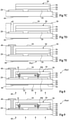
- the picture 2 is a top view, partial and schematic, of an embodiment of a photodetector Pix1 which can correspond to one of the photodetectors Pix of the detection device 10.
- the picture 3 is a cut of the picture 2 along line III-III.
- the outline of a conductive or semi-conductive portion covered, in top view, by another conductive or semi-conductive portion has been shown in dotted lines.
- FIG 4 is a partial and schematic top view of another embodiment of a photodetector Pix2 which can correspond to one of the photodetectors Pix of the detection device 10.
- figure 5 is a cut of the figure 4 along line VV and
- figure 6 is a cut of the figure 4 along line VI-VI.
- the outline of a conductive or semi-conductive portion covered, in top view, by another conductive or semi-conductive portion has been shown in dotted lines.
- the Pix2 photodetector shown in figures 4 to 6 includes all the elements of the Pix1 photodetector represented on the figures 2 and 3 with the difference that the conductive element 40 is not present and that the conductive track 12 is produced by the conductive portion 28.
- the crossing between the conductive portions 26 and 28 is achieved by interrupting the conductive portion 26 and by providing a bridge conductor 46 which connects the two separate parts of the conductive portion 26 and which spans the conductive portion 28.
- the conductive bridge 46 is electrically insulated from the conductive portion 28 by an insulating region 48.
- the interface layer 32 and the active layer 34 can advantageously extend over the entire surface of the Pix2 photodetector.
- the support 20 can be made of a dielectric material.
- the support 20 can be a rigid support, for example made of glass.
- the support 20 can be a flexible support, for example in one polymer or metallic material. Examples of polymer are polyethylene naphthalene (PEN), polyethylene terephthalate (PET), kapton, and polyetheretherketone (PEEK).
- the thickness of the support 20 is, for example, between 20 ⁇ m and 1 cm, for example around 125 ⁇ m.
- the support 20 can be made of a transparent or translucent material, for example glass or plastic, in particular in the case where the device 10 is intended to receive illumination from the side of the face 24.
- the conductive portions 26 and 28 can be in a conductive and transparent material, for example in conductive and transparent oxide or TCO (acronym for Transparent Conductive Oxide), in carbon nanotubes, in graphene, in a conductive polymer, in a metal, or a mixture or an alloy of at least two of these compounds.
- TCO conductive and transparent oxide
- the conductive portions 26 and 28 can have a multilayer structure.
- ITO indium-tin oxide
- AZO aluminum-zinc oxide
- GZO gallium-zinc oxide
- conductive polymers suitable for producing conductive portions 26 and 28 are the polymer known under the name PEDOT:PSS, which is a mixture of poly(3,4)-ethylenedioxythiophene and sodium polystyrene sulfonate, and polyaniline, also called PAni.
- Examples of metals suitable for making the conductive portions 26 and 28 are silver (Ag), aluminum (Al), gold (Au), copper (Cu), nickel (Ni), titanium (Ti) and chromium (Cr).
- An example of a multilayer structure suitable for producing the conductive portions 26 and 28 is a multilayer structure of AZO and silver of the AZO/Ag/AZO type.
- the thickness of the conductive portions 26 and 28 can be between 5 nm and 30 ⁇ m, for example around 150 nm. In the case where the conductive portions 26, 28 are metallic and must be at least partially transparent, the thickness of the conductive portions 26, 28 is less than or equal to 20 nm, preferably less than or equal to 10 nm.
- the minimum difference between the conductive portion 26 and the conductive portion 28 of the photodetector Pix1, Pix2 is greater than or equal to 10 nm, preferably greater than or equal to 1 ⁇ m, more preferably between 10 ⁇ m and 500 ⁇ m.
- the interface layer 32 or 36 may correspond to an electron injector layer or to a hole injector layer depending on whether this interface layer plays the role of a cathode or an anode.
- the output function of interface layer 32 or 36 is suitable for blocking, collecting or injecting holes and/or electrons depending on whether this interface layer acts as a cathode or an anode. More precisely, when the interface layer 32 or 36 acts as an anode, it corresponds to a hole injector and electron blocker layer.
- the work function of interface layer 32 or 36 is then greater than or equal to 4.5 eV, preferably greater than or equal to 5 eV.
- the interface layer 32 or 36 acts as a cathode, it corresponds to an electron-injecting and hole-blocking layer.
- the work function of interface layer 32 or 36 is then less than or equal to 5 eV, preferably less than or equal to 4.2 eV.
- the first interface layer 32 acts as an electron injector layer and is made of ethoxylated polyethyleneimine polymer.
- the thickness of interface layer 32 is preferably between 0.1 nm and 500 nm.
- the interface layer 32 has an electrical resistance greater than 10 9 ⁇ / ⁇ , preferably greater than or equal to 10 12 ⁇ / ⁇ . The high electrical resistance of the interface layer 32 prevents the formation of a short circuit with the conductive portions 26, 28.
- the material forming the interface layer 32 or 36 is a doped conductive or semi-conductive polymer.
- the second interface layer 36 acts as a hole injector layer and is made of PEDOT:PSS.
- PEDOT:PSS An advantage of PEDOT:PSS is that it can be easily deposited by printing techniques, for example by inkjet, by heliography, by screen printing, by coating by die (in English slot-die coating) or by coating.
- Interface layer 36 provides a conductive path between diode D and photodiode PH.
- the thickness of interface layer 36 is preferably between 10 nm and 50 ⁇ m.
- the interface layer 36 has an electrical resistance of less than 10k ⁇ / ⁇ , preferably less than or equal to 1k ⁇ / ⁇ . The low electrical resistance of the interface layer 36 makes it possible to reduce the response time and to improve the linearity of the device.
- the active layer 34 can comprise small molecules, oligomers or polymers. They can be organic or inorganic materials.
- the active layer 34 may comprise an ambipolar semiconductor material, or a mixture of an N-type semiconductor material and a P-type semiconductor material, for example in the form of superimposed layers or an intimate mixture at the nanometric scale. so as to form a bulk heterojunction.
- the thickness of the active layer 34 can be between 50 nm and 1 ⁇ m, for example around 300 nm.
- P-type semiconductor polymers suitable for producing the active layer 34 are poly(3-hexylthiophene) (P3HT), poly[N-9'-heptadecanyl-2,7-carbazole-alt-5,5 -(4,7-di-2-thienyl-2',1',3'-benzothiadiazole] (PCDTBT), poly[(4,8-bis-(2-ethylhexyloxy)-benzo[1,2-b ;4,5-b']dithiophene)-2,6-diyl-alt-(4-(2-ethylhexanoyl)-thieno[3,4-b]thiophene))-2,6-diyl] (PBDTTT-C ), poly[2-methoxy-5-(2-ethyl-hexyloxy)-1,4-phenylene-vinylene] (MEH-PPV) or poly[2,6-(4,4-bis-(2- ethyl)
- N-type semiconductor materials suitable for producing the active layer 34 are fullerenes, in particular C60, [6,6]-phenyl-C 61 -methyl butanoate ([60]PCBM), [6 methyl ,6]-phenyl-C 71 -butanoate ([70]PCBM), perylene diimide, zinc oxide (ZnO) or nanocrystals allowing the formation of quantum dots.
- the insulating layer 38 can have a thickness comprised between 500 nm and 100 ⁇ m, for example approximately 2 ⁇ m.
- the insulating layer 38 can have a monolayer structure or a multilayer structure.
- the insulating layer 38 can be made of fluorinated polymer, in particular the fluorinated polymer marketed under the name Cytop by the company Bellex, in polyvinylpyrrolidone (PVP), in polymethyl methacrylate (PMMA), in polystyrene (PS), in parylene, in polyimide (PI) or a mixture of at least two of these compounds.
- Layer 38 can be deposited as a solution.
- the opaque region 44 can be made of a carbon-based ink, graphene, a metal, or a mixture or an alloy of at least two of these compounds.
- the opaque region 44 can have a thickness comprised between 10 nm and 100 ⁇ m, for example around 10 ⁇ m.
- Conductive bridge 46 can be made of conductive material, for example PEDOT:PSS, silver ink or carbon ink.
- the thickness of conductive bridge 46 can be between 10 nm and 50 ⁇ m.
- the insulating region 48 can be made of dielectric material deposited in solution.
- the thickness of insulating region 48 can be between 100 nm and 100 ⁇ m.
- the support 20, the conductive portions 26 and the first interface layer 32 are at least partially transparent to the electromagnetic radiation detected by the detection device.
- radiation reaching the photodetector Pix on the side of the face 24 has been schematically represented by arrows 49.
- the second interface layer 36 and/or the insulating layer 38 can then be at least partly opaque to the radiation so as to reduce the risks of undesirable illumination of the active layer 34 by the face 39.
- the insulating layer 38 and the second interface layer 36 are made of at least partially transparent materials.
- the support 20, the conductive portions 26, 28 and/or the first interface layer 32 can then be at least partly opaque to radiation so as to reduce the risks of undesirable illumination of the active layer 34 by the face 24.
- the support 20, the conductive portions 26, 28 and the insulating layer 38 are made of materials with less partly transparent.
- the photodetector Pix1, Pix2 is intended to receive illumination from the side of the face 39 of the insulating layer 38 and in the case where the support 20 is, moreover, at least partly transparent to the radiation received by the photodetector, the conductive portions 26, 28 can be at least partly opaque to radiation so as to reduce the propagation of light in the support 20 as far as the diode D.
- the opaque region 44 prevents the radiation from reaching a part of the stack 30 which then functions as a diode while the rest of the stack 30, which receives the radiation, functions as a PH photodiode.
- the material making up the interface layer 36 is chosen with a suitable resistivity so that substantially all of the charges circulate between the conductive portions 26 and 28 by crossing the active layer 34 of the stack 30 twice, once in the portion of the stack 30 concealed by the opaque region 44 and once in the part of the stack 30 receiving the electromagnetic radiation.
- a connection is indeed obtained between the photodiode PH and the common anode or common cathode diode D.
- the electrical symbols for diode D and photodiode PH have been added.
- the figures 7A to 7E illustrate steps of an embodiment of a method of manufacturing the photodetector Pix1.
- the Figure 7A represents the structure obtained after having formed the conductive portions 26 and 28 on the face 22 of the support 20 and the opaque region 44 on the face 24 of the support 20.
- the process for forming the conductive portions 26, 28 and the opaque region 44 may correspond to a so-called additive process, for example by direct deposition of the material making up the conductive portions 26, 28 or the opaque region 44 at the locations desired.
- the deposition can be carried out by inkjet printing, heliography, screen printing, flexography, spray coating (in English spray coating) or deposition of drops (in English drop-casting).
- the process for forming the conductive portions 26, 28 and/or the opaque region 44 may correspond to a so-called subtractive process, in which a layer of the material making up the conductive portions 26, 28 and/or the opaque region 44 is deposited on the entire structure and in which the unused portions are then removed, for example by photolithography or laser ablation.
- the deposition on the entire structure can be carried out for example by liquid means, by sputtering or by evaporation. These may include processes such as spin coating, spray coating, dipping, heliography, slot-die coating, blade-coating, flexography or screen printing.
- the conductive portions 26, 28 and/or the opaque region 44 are metallic, the metal is, for example, deposited by evaporation or by sputtering on the whole of the support 20 and the conductive portions 26, 28 and/or the region opaque 44 are marked out by engraving.
- the materials making up the conductive portions 26, 28 are different, in particular when the conductive portions 26 are opaque, the conductive portions 26, 28 can be formed in separate steps.
- the figure 7B represents the structure obtained after having successively deposited the layers 32, 34, 36 on the whole of the support 20.
- the layers 34 and 36 can be produced by die coating.
- Layer 32 can be produced by immersing the structure in a bath of the material making up the layer in question, after having removed the structure from the bath and after having dried the structure.
- An annealing step can be provided after the deposition of each layer 32, 34, 36 or after the deposition of some of the layers 32, 34, 36, in particular the layer 32.
- a surface treatment can be provided after the deposition of each layer 32, 34, 36 or after the deposition of some of the layers 32, 34, 36, in particular layer 34, to improve the deposition of the following layer.
- the surface treatment may comprise a plasma cleaning step, for example an oxygen plasma obtained by an inductively coupled plasma source comprising a radiofrequency power generator whose power may be 500 W, in a reactor at a pressure of the order of 133 Pa (about 1 Torr) for 1 minute.
- a plasma cleaning step for example an oxygen plasma obtained by an inductively coupled plasma source comprising a radiofrequency power generator whose power may be 500 W, in a reactor at a pressure of the order of 133 Pa (about 1 Torr) for 1 minute.
- the Fig. 7C represents the structure obtained after having etched the layers 32, 34 and 36 to delimit the stack 30.
- the etching may be reactive ion etching (RIE, English acronym for Reactive Ion Etching).
- RIE reactive ion etching
- the stack 30 can be formed by the additive deposition methods or the other subtractive deposition methods described previously.
- the figure 7D represents the structure obtained after a step of depositing the insulating layer 38 over the entire structure and a step of forming the opening 42 in the insulating layer 38 for each photodetector Pix1.
- the insulating layer 38 can be deposited according to the additive deposition methods described previously.
- the opening 42 can be made by RIE.
- the figure 7E represents the structure obtained after the formation of the conductive element 40.
- the conductive element 40 can be deposited according to the additive or subtractive deposition methods described previously.
- the following steps of the manufacturing process include in particular the encapsulation of the Pix1 photodetectors, for example by covering the faces 24 and 39 of the structure shown in figure 7E of a protective layer, and possibly the cutting of the support 20 to delimit the detection device 10.
- the detection device 10 can be produced by printing techniques.
- the materials of the conductive portions 26, 28, of the layers 32, 34, 36, of the conductive element 40 and/or of the opaque region 44 can be deposited in liquid form, for example in the form of conductive and semi-conductive inks.
- Materials in liquid form here also means gel materials that can be deposited by printing techniques.
- Annealing steps are optionally provided between the depositions of the different layers, but the annealing temperatures may not exceed 150° C., and the deposition and any annealings may be carried out at atmospheric pressure.
- the occultation of the diode D with respect to the radiation received by the detection device is obtained by the formation of the opaque region 44 on the face 24 of the support 22.
- figures 8 and 9 represent other embodiments of the occultation of the diode D suitable for photodetectors intended to receive light radiation from the side of the face 24 of the support 20.
- the figure 8 represents another embodiment of a Pix3 photodetector.
- the Pix3 photodetector comprises all the elements of the Pix1 photodetector except that the opaque region 44 is not formed on the face 24 of the support 20 but is provided on a face 50 of a coating 52 fixed to the face 24.
- Coating 52 includes an at least partially transparent layer to the radiation detected by the photodiode PH, for example a layer of PET having a thickness of 125 ⁇ m.
- the coating 52 can be fixed to the support 20 by lamination, a layer of glue 54 being able to be interposed between the layer 52 and the face 24.
- the figure 9 shows another embodiment of a Pix4 photodetector.
- the photodetector Pix4 comprises all the elements of the photodetector Pix1 except that the opaque region 44 is not present.
- the occultation of the diode D is carried out by the conductive portion 28 which is substantially opaque to the radiation detected by the photodiode PH whereas the conductive portion 26 is at least partially transparent to this radiation.
- the conductive portion 28 is made of a different material from the conductive portion 26.
- the opaque conductive portion 28 is made of metallic materials or corresponds to a deposit of the graphene or graphite type and the conductive portion 26 transparent is made of TCO, Ag nanowires, or carbon nanotubes. This embodiment advantageously makes it possible to bring the occultation screen closer to diode D.
- the embodiments represented on the figures 10 to 13 are adapted to photodetectors intended to receive light radiation from the side of the face 39 of the insulating layer 38.
- Photodetector Pix5 comprises all the elements of photodetector Pix1 except that opaque region 44 is not formed on face 24 of support 20 but is provided on face 39 of insulating layer 38.
- the figure 11 shows another embodiment of a Pix6 photodetector.
- the Pix6 photodetector comprises all the elements of the Pix5 photodetector except that the opaque region 44 is not formed on the face 39 of the insulating layer 38 but is provided on a face 57 of a coating 58 fixed to the face 39 of the insulating layer 38.
- the coating 58 comprises an insulating layer and at least partly transparent to the radiation detected by the photodiode PH, for example a layer of PET having a thickness of 125 ⁇ m.
- the coating 58 can be fixed to the insulating layer 38 by lamination, an adhesive layer 60 being able to be interposed between the coating 58 and the insulating layer 38.
- the figure 12 shows another embodiment of a Pix7 photodetector.
- the Pix7 photodetector comprises all the elements of the Pix5 photodetector except that the occultation function performed by the opaque region 44 for the Pix5 photodetector is performed directly by the conductive element 40, the part of which extends over the face 39 of the insulating layer 38 has a shape adapted to prevent the radiation 56 received by the photodetector Pix7 from reaching the diode D.
- the manufacturing method of the photodetector Pix7 advantageously comprises a reduced number of steps.
- the figure 13 shows another embodiment of a Pix8 photodetector.
- the Pix8 photodetector comprises all the elements of the Pix7 photodetector except that the occultation function is performed by a conductive region 62, located on the face 39 of the insulating layer 38, which is composed of the same material as the element conductive element 40 and is produced simultaneously with the conductive element 40 but which is not electrically connected to the conductive element 40.
- the present embodiment advantageously makes it possible to prevent the opaque region 62 from degrading the properties conduction of the conductive element 40, in particular by the injection of noise, during the operation of the detection device 10.
- a first opaque screen preventing the exposure of the diode D of each photodetector to radiation can be provided on the side of the face 24 according to one of the embodiments described previously and represented on the figure 2 , 8 or 9 and a second opaque screen preventing the exposure of the diode D of each photodetector to radiation can be provided on the side of the face 39 according to one of the embodiments described previously and represented on the figures 10 to 13 .
Landscapes
- Engineering & Computer Science (AREA)
- Chemical & Material Sciences (AREA)
- Materials Engineering (AREA)
- Physics & Mathematics (AREA)
- Electromagnetism (AREA)
- Light Receiving Elements (AREA)
- Solid State Image Pick-Up Elements (AREA)
- Manufacturing & Machinery (AREA)
Claims (11)
- Eine Vorrichtung (10) zum Detektieren einer elektromagnetischen Strahlung (49; 56), die mindestens einen Fotodetektor (Pix; Pix1) aufweist, der eine organische Diode (D), die sich von einer Leuchtdiode unterscheidet, und eine organische Fotodiode (PH) aufweist, die in einem gleichen Stapel (30) von Halbleiterschichten (32, 34, 36) gebildet ist, wobei die organische Fotodiode die genannte Strahlung empfängt, wobei der Fotodetektor ferner mindestens einen Schirm (44) aufweist, der für die genannte Strahlung opak bzw. undurchlässig ist und den der Diode entsprechenden Teil des Stapels abschirmt.
- Die Vorrichtung zum Detektieren nach Anspruch 1, wobei die Anode der Diode (D) mit der Anode der Photodiode (PH) verbunden ist oder wobei die Kathode der Diode mit der Kathode der Photodiode verbunden ist.
- Die Vorrichtung zum Detektieren nach Anspruch 1 oder 2, die Folgendes aufweist: einen Träger (20), einen ersten leitenden Abschnitt (26), der sich über den Träger erstreckt, und einen zweiten leitenden Abschnitt (28), der sich über den Träger erstreckt, wobei der Stapel (30) den ersten leitenden Abschnitt zumindest teilweise und den zweiten leitenden Abschnitt zumindest teilweise bedeckt, wobei der Mindestabstand zwischen dem ersten leitenden Abschnitt und dem zweiten leitenden Abschnitt größer als 10 nm ist.
- Die Vorrichtung zum Detektieren nach Anspruch 3, wobei sich der opake Schirm (44) auf der Seite des Trägers (20) befindet, die dem ersten und zweiten leitenden Abschnitt (26, 28) gegenüberliegt.
- Die Vorrichtung zum Detektieren nach Anspruch 3, wobei der erste leitende Abschnitt (26) für die Strahlung zumindest teilweise transparent ist und wobei der zweite leitende Abschnitt (28) für die Strahlung opak bzw. undurchsichtig ist.
- Die Vorrichtung zum Detektieren nach Anspruch 3, die ferner eine den Stapel (30) bedeckende Isolierschicht (38) aufweist, wobei der opake Schirm (44) auf der Isolierschicht, und zwar auf der dem Stapel gegenüberliegenden Seite der Isolierschicht angeordnet ist.
- Die Vorrichtung zum Detektieren nach Anspruch 6, die ferner ein leitendes Element (40) aufweist, das sich über die Isolierschicht (38) und durch die Isolierschicht hindurch erstreckt, wobei das leitende Element (40) in Kontakt mit dem ersten leitenden Abschnitt (26) oder mit dem zweiten leitenden Abschnitt (28) steht, wobei das leitende Element (40) ferner den opaken Schirm bildet.
- Die Vorrichtung zum Detektieren nach einem der Ansprüche 1 bis 7, die eine Anordnung von Photodetektoren (Pix) aufweist, die in Zeilen und Spalten aufgeteilt bzw. verteilt sind.
- Die Vorrichtung zum Detektieren nach einem der Ansprüche 1 bis 8, wobei der Stapel (30) mindestens erste, zweite und dritte Halbleiterschichten aufweist, wobei die zweite Halbleiterschicht (34) zwischen der ersten Halbleiterschicht (32) und der dritten Halbleiterschicht (36) angeordnet ist und mit der ersten Halbleiterschicht und der dritten Halbleiterschicht in Kontakt steht, wobei die zweite jene Schicht ist, in der der größte Anteil der von der Fotodiode (PH) empfangenen Strahlung eingefangen wird.
- Die Vorrichtung zum Detektieren nach Anspruch 9 rückbezogen auf Anspruch 3, wobei die erste Halbleiterschicht (32) mit dem ersten leitenden Abschnitt (26) und mit dem zweiten leitenden Abschnitt (28) in Kontakt steht.
- Die Vorrichtung zum Detektieren nach Anspruch 9 oder 10, wobei die erste Halbleiterschicht (32) und/oder die dritte Halbleiterschicht (36) aus einem Material hergestellt ist bzw. sind, das ausgewählt ist aus der Gruppe, die Folgendes aufweist:ein Metalloxid, insbesondere ein Titanoxid oder ein Zinkoxid;ein molekulares Wirts-/Dotierstoffsystem;ein leitfähiges oder dotiertes Halbleiterpolymer, zum Beispiel das Polymer PEDOT:Tosylat, das eine Mischung aus Poly(3,4)-Ethylendioxythiophen und Tosylat ist;ein Carbonat, zum Beispiel CsCO3;ein Polyelektrolyt, zum Beispiel aus Poly[9,9-bis(3'-(N,N-dimethylamino)propyl)-2,7-fluoren-alt-2,7-(9,9-dioctyfluoren)] (PFN), aus Poly[3-(6-trimethylammoniumhexyl]thiophen (P3TMAHT) oder aus Poly[9,9-bis(2-ethylhexyl)fluoren]-b-poly[3-(6-trimethyl-ammoniumhexyl]thiophen (PF2/6-b-P3TMAHT);ein Polymer aus Polyethylenimin (PEI) oder ein Polymer vom Polymer aus ethoxyliertem Polyethylenimin (PEIE), propoxyliertem Polyethylenimin und/oder butoxyliertem Polyethylenimin; undein Gemisch aus zwei oder mehr als zwei dieser Materialien.
Applications Claiming Priority (2)
| Application Number | Priority Date | Filing Date | Title |
|---|---|---|---|
| FR1753424A FR3065583B1 (fr) | 2017-04-20 | 2017-04-20 | Dispositif de detection d'un rayonnement comprenant des photodiodes organiques |
| PCT/FR2018/050982 WO2018193216A1 (fr) | 2017-04-20 | 2018-04-19 | Dispositif de detection d'un rayonnement comprenant des photodiodes organiques |
Publications (2)
| Publication Number | Publication Date |
|---|---|
| EP3613080A1 EP3613080A1 (de) | 2020-02-26 |
| EP3613080B1 true EP3613080B1 (de) | 2022-03-09 |
Family
ID=59070894
Family Applications (1)
| Application Number | Title | Priority Date | Filing Date |
|---|---|---|---|
| EP18723573.4A Active EP3613080B1 (de) | 2017-04-20 | 2018-04-19 | Strahlungsdetektionsvorrichtung, organische fotodioden umfassend |
Country Status (7)
| Country | Link |
|---|---|
| US (1) | US11189664B2 (de) |
| EP (1) | EP3613080B1 (de) |
| JP (1) | JP2020518132A (de) |
| KR (1) | KR102509826B1 (de) |
| CN (1) | CN110770910B (de) |
| FR (1) | FR3065583B1 (de) |
| WO (1) | WO2018193216A1 (de) |
Families Citing this family (4)
| Publication number | Priority date | Publication date | Assignee | Title |
|---|---|---|---|---|
| FR3098821B1 (fr) | 2019-07-19 | 2023-05-26 | Isorg | Encre pour une couche d’injection d’électrons |
| KR20220015111A (ko) * | 2020-07-30 | 2022-02-08 | 엘지디스플레이 주식회사 | 표시장치와 이를 포함한 모바일 단말기 |
| KR102429196B1 (ko) * | 2020-10-16 | 2022-08-05 | 중앙대학교 산학협력단 | 유연 구조 포토디텍터 |
| WO2023112814A1 (ja) * | 2021-12-15 | 2023-06-22 | 株式会社ジャパンディスプレイ | 検出装置 |
Family Cites Families (12)
| Publication number | Priority date | Publication date | Assignee | Title |
|---|---|---|---|---|
| JP4170026B2 (ja) * | 2002-06-18 | 2008-10-22 | 住友化学株式会社 | コプラナー型有機光−光変換デバイス |
| CN101908556A (zh) * | 2003-12-17 | 2010-12-08 | 住友化学株式会社 | 有机光-光变换装置 |
| JP5615174B2 (ja) * | 2007-07-23 | 2014-10-29 | ビーエーエスエフ ソシエタス・ヨーロピアBasf Se | 光起電力タンデム電池 |
| JP5794068B2 (ja) | 2011-09-16 | 2015-10-14 | ソニー株式会社 | 固体撮像素子および製造方法、並びに電子機器 |
| US9685567B2 (en) * | 2012-07-20 | 2017-06-20 | Nutech Ventures | Nanocomposite photodetector |
| DE102012213410B3 (de) * | 2012-07-31 | 2013-09-19 | Siemens Aktiengesellschaft | Röntgenstrahlungsdetektor und CT-System |
| DE102012220056A1 (de) * | 2012-11-02 | 2014-02-13 | Osram Opto Semiconductors Gmbh | Organisches optoelektronisches bauelement und verfahren zum betrieb des organischen optoelektronischen bauelements |
| DE102012222772B4 (de) * | 2012-12-11 | 2021-09-16 | Pictiva Displays International Limited | Organisches optoelektronisches Bauelement |
| DE102013201212A1 (de) * | 2013-01-25 | 2014-07-31 | Osram Opto Semiconductors Gmbh | Verfahren zum Betrieb eines organischen optoelektronischen Bauelements |
| WO2016014345A2 (en) * | 2014-07-23 | 2016-01-28 | Cbrite Inc. | Two-terminal electronic devices and their methods of fabrication |
| JP2017004745A (ja) * | 2015-06-10 | 2017-01-05 | 日立金属株式会社 | ノイズシールドケーブル |
| JP7002475B2 (ja) * | 2017-01-15 | 2022-01-20 | サイントル株式会社 | 光検出器アレイ |
-
2017
- 2017-04-20 FR FR1753424A patent/FR3065583B1/fr active Active
-
2018
- 2018-04-19 WO PCT/FR2018/050982 patent/WO2018193216A1/fr unknown
- 2018-04-19 JP JP2019556952A patent/JP2020518132A/ja active Pending
- 2018-04-19 CN CN201880040766.9A patent/CN110770910B/zh active Active
- 2018-04-19 US US16/606,583 patent/US11189664B2/en active Active
- 2018-04-19 KR KR1020197033964A patent/KR102509826B1/ko active IP Right Grant
- 2018-04-19 EP EP18723573.4A patent/EP3613080B1/de active Active
Also Published As
| Publication number | Publication date |
|---|---|
| US11189664B2 (en) | 2021-11-30 |
| WO2018193216A1 (fr) | 2018-10-25 |
| KR102509826B1 (ko) | 2023-03-13 |
| FR3065583A1 (fr) | 2018-10-26 |
| CN110770910A (zh) | 2020-02-07 |
| JP2020518132A (ja) | 2020-06-18 |
| CN110770910B (zh) | 2023-08-01 |
| FR3065583B1 (fr) | 2019-06-28 |
| KR20200008565A (ko) | 2020-01-28 |
| US20210118954A1 (en) | 2021-04-22 |
| EP3613080A1 (de) | 2020-02-26 |
Similar Documents
| Publication | Publication Date | Title |
|---|---|---|
| EP3613080B1 (de) | Strahlungsdetektionsvorrichtung, organische fotodioden umfassend | |
| FR3063564A1 (fr) | Capteur d'empreintes digitales integre dans un ecran d'affichage | |
| WO2016202938A1 (fr) | Procédé de réalisation d'un empilement du type première électrode / couche active / deuxième électrode | |
| EP3477721A1 (de) | Elektronische oder hybride vorrichtung und hestellungsvarfahren dazu | |
| EP3394893B1 (de) | Optoelektronische matrixanordnung mit transparenter oberer elektrode | |
| WO2021043707A1 (fr) | Pixel d'ecran d'affichage | |
| EP3183749B1 (de) | Vorrichtung zur detektion von elektromagnetischer strahlung aus organischen materialen | |
| EP3111480B1 (de) | Elektronische vorrichtung mit organischer optoelektronischer komponente und zwei organischen transistoren | |
| EP3331017B1 (de) | Infrarot-fotosensor | |
| WO2019234339A1 (fr) | Dispositif optoelectronique et son procede de fabrication | |
| EP4000110A1 (de) | Optoelektronische vorrichtung mit einer aktiven organischen schicht mit verbesserter leistung und verfahren zur herstellung dieser vorrichtung | |
| WO2018206902A1 (fr) | Dispositif electronique a tenue au vieillissement amelioree | |
| EP3552243B1 (de) | Lichtdetektor mit ladungsträgersammelschicht mit funktionalisierten nanodrähten | |
| WO2021116232A1 (fr) | Capteur d'images pour correction du bruit electronique d'un capteur | |
| FR3091034A1 (fr) | Dispositif électronique à courant de fuite réduit | |
| EP3491673A1 (de) | Optoelektronische vorrichtung und herstellungsverfahren dafür | |
| WO2020193889A1 (fr) | Capteur d'images comprenant un filtre angulaire |
Legal Events
| Date | Code | Title | Description |
|---|---|---|---|
| STAA | Information on the status of an ep patent application or granted ep patent |
Free format text: STATUS: UNKNOWN |
|
| STAA | Information on the status of an ep patent application or granted ep patent |
Free format text: STATUS: THE INTERNATIONAL PUBLICATION HAS BEEN MADE |
|
| PUAI | Public reference made under article 153(3) epc to a published international application that has entered the european phase |
Free format text: ORIGINAL CODE: 0009012 |
|
| STAA | Information on the status of an ep patent application or granted ep patent |
Free format text: STATUS: REQUEST FOR EXAMINATION WAS MADE |
|
| 17P | Request for examination filed |
Effective date: 20191104 |
|
| AK | Designated contracting states |
Kind code of ref document: A1 Designated state(s): AL AT BE BG CH CY CZ DE DK EE ES FI FR GB GR HR HU IE IS IT LI LT LU LV MC MK MT NL NO PL PT RO RS SE SI SK SM TR |
|
| AX | Request for extension of the european patent |
Extension state: BA ME |
|
| DAV | Request for validation of the european patent (deleted) | ||
| DAX | Request for extension of the european patent (deleted) | ||
| RAP1 | Party data changed (applicant data changed or rights of an application transferred) |
Owner name: ISORG |
|
| REG | Reference to a national code |
Ref country code: DE Ref legal event code: R079 Ref document number: 602018031954 Country of ref document: DE Free format text: PREVIOUS MAIN CLASS: H01L0027280000 Ipc: H01L0027300000 |
|
| GRAP | Despatch of communication of intention to grant a patent |
Free format text: ORIGINAL CODE: EPIDOSNIGR1 |
|
| STAA | Information on the status of an ep patent application or granted ep patent |
Free format text: STATUS: GRANT OF PATENT IS INTENDED |
|
| RIC1 | Information provided on ipc code assigned before grant |
Ipc: H01L 27/30 20060101AFI20211011BHEP |
|
| INTG | Intention to grant announced |
Effective date: 20211112 |
|
| GRAS | Grant fee paid |
Free format text: ORIGINAL CODE: EPIDOSNIGR3 |
|
| GRAA | (expected) grant |
Free format text: ORIGINAL CODE: 0009210 |
|
| STAA | Information on the status of an ep patent application or granted ep patent |
Free format text: STATUS: THE PATENT HAS BEEN GRANTED |
|
| AK | Designated contracting states |
Kind code of ref document: B1 Designated state(s): AL AT BE BG CH CY CZ DE DK EE ES FI FR GB GR HR HU IE IS IT LI LT LU LV MC MK MT NL NO PL PT RO RS SE SI SK SM TR |
|
| REG | Reference to a national code |
Ref country code: CH Ref legal event code: EP Ref country code: AT Ref legal event code: REF Ref document number: 1474868 Country of ref document: AT Kind code of ref document: T Effective date: 20220315 |
|
| REG | Reference to a national code |
Ref country code: IE Ref legal event code: FG4D Free format text: LANGUAGE OF EP DOCUMENT: FRENCH |
|
| REG | Reference to a national code |
Ref country code: DE Ref legal event code: R096 Ref document number: 602018031954 Country of ref document: DE |
|
| REG | Reference to a national code |
Ref country code: LT Ref legal event code: MG9D |
|
| REG | Reference to a national code |
Ref country code: NL Ref legal event code: MP Effective date: 20220309 |
|
| PG25 | Lapsed in a contracting state [announced via postgrant information from national office to epo] |
Ref country code: SE Free format text: LAPSE BECAUSE OF FAILURE TO SUBMIT A TRANSLATION OF THE DESCRIPTION OR TO PAY THE FEE WITHIN THE PRESCRIBED TIME-LIMIT Effective date: 20220309 Ref country code: RS Free format text: LAPSE BECAUSE OF FAILURE TO SUBMIT A TRANSLATION OF THE DESCRIPTION OR TO PAY THE FEE WITHIN THE PRESCRIBED TIME-LIMIT Effective date: 20220309 Ref country code: NO Free format text: LAPSE BECAUSE OF FAILURE TO SUBMIT A TRANSLATION OF THE DESCRIPTION OR TO PAY THE FEE WITHIN THE PRESCRIBED TIME-LIMIT Effective date: 20220609 Ref country code: LT Free format text: LAPSE BECAUSE OF FAILURE TO SUBMIT A TRANSLATION OF THE DESCRIPTION OR TO PAY THE FEE WITHIN THE PRESCRIBED TIME-LIMIT Effective date: 20220309 Ref country code: HR Free format text: LAPSE BECAUSE OF FAILURE TO SUBMIT A TRANSLATION OF THE DESCRIPTION OR TO PAY THE FEE WITHIN THE PRESCRIBED TIME-LIMIT Effective date: 20220309 Ref country code: BG Free format text: LAPSE BECAUSE OF FAILURE TO SUBMIT A TRANSLATION OF THE DESCRIPTION OR TO PAY THE FEE WITHIN THE PRESCRIBED TIME-LIMIT Effective date: 20220609 |
|
| REG | Reference to a national code |
Ref country code: AT Ref legal event code: MK05 Ref document number: 1474868 Country of ref document: AT Kind code of ref document: T Effective date: 20220309 |
|
| PG25 | Lapsed in a contracting state [announced via postgrant information from national office to epo] |
Ref country code: LV Free format text: LAPSE BECAUSE OF FAILURE TO SUBMIT A TRANSLATION OF THE DESCRIPTION OR TO PAY THE FEE WITHIN THE PRESCRIBED TIME-LIMIT Effective date: 20220309 Ref country code: GR Free format text: LAPSE BECAUSE OF FAILURE TO SUBMIT A TRANSLATION OF THE DESCRIPTION OR TO PAY THE FEE WITHIN THE PRESCRIBED TIME-LIMIT Effective date: 20220610 Ref country code: FI Free format text: LAPSE BECAUSE OF FAILURE TO SUBMIT A TRANSLATION OF THE DESCRIPTION OR TO PAY THE FEE WITHIN THE PRESCRIBED TIME-LIMIT Effective date: 20220309 |
|
| PG25 | Lapsed in a contracting state [announced via postgrant information from national office to epo] |
Ref country code: NL Free format text: LAPSE BECAUSE OF FAILURE TO SUBMIT A TRANSLATION OF THE DESCRIPTION OR TO PAY THE FEE WITHIN THE PRESCRIBED TIME-LIMIT Effective date: 20220309 |
|
| PG25 | Lapsed in a contracting state [announced via postgrant information from national office to epo] |
Ref country code: SM Free format text: LAPSE BECAUSE OF FAILURE TO SUBMIT A TRANSLATION OF THE DESCRIPTION OR TO PAY THE FEE WITHIN THE PRESCRIBED TIME-LIMIT Effective date: 20220309 Ref country code: SK Free format text: LAPSE BECAUSE OF FAILURE TO SUBMIT A TRANSLATION OF THE DESCRIPTION OR TO PAY THE FEE WITHIN THE PRESCRIBED TIME-LIMIT Effective date: 20220309 Ref country code: RO Free format text: LAPSE BECAUSE OF FAILURE TO SUBMIT A TRANSLATION OF THE DESCRIPTION OR TO PAY THE FEE WITHIN THE PRESCRIBED TIME-LIMIT Effective date: 20220309 Ref country code: PT Free format text: LAPSE BECAUSE OF FAILURE TO SUBMIT A TRANSLATION OF THE DESCRIPTION OR TO PAY THE FEE WITHIN THE PRESCRIBED TIME-LIMIT Effective date: 20220711 Ref country code: ES Free format text: LAPSE BECAUSE OF FAILURE TO SUBMIT A TRANSLATION OF THE DESCRIPTION OR TO PAY THE FEE WITHIN THE PRESCRIBED TIME-LIMIT Effective date: 20220309 Ref country code: EE Free format text: LAPSE BECAUSE OF FAILURE TO SUBMIT A TRANSLATION OF THE DESCRIPTION OR TO PAY THE FEE WITHIN THE PRESCRIBED TIME-LIMIT Effective date: 20220309 Ref country code: CZ Free format text: LAPSE BECAUSE OF FAILURE TO SUBMIT A TRANSLATION OF THE DESCRIPTION OR TO PAY THE FEE WITHIN THE PRESCRIBED TIME-LIMIT Effective date: 20220309 Ref country code: AT Free format text: LAPSE BECAUSE OF FAILURE TO SUBMIT A TRANSLATION OF THE DESCRIPTION OR TO PAY THE FEE WITHIN THE PRESCRIBED TIME-LIMIT Effective date: 20220309 |
|
| REG | Reference to a national code |
Ref country code: DE Ref legal event code: R079 Ref document number: 602018031954 Country of ref document: DE Free format text: PREVIOUS MAIN CLASS: H01L0027300000 Ipc: H10K0039000000 |
|
| PG25 | Lapsed in a contracting state [announced via postgrant information from national office to epo] |
Ref country code: PL Free format text: LAPSE BECAUSE OF FAILURE TO SUBMIT A TRANSLATION OF THE DESCRIPTION OR TO PAY THE FEE WITHIN THE PRESCRIBED TIME-LIMIT Effective date: 20220309 Ref country code: IS Free format text: LAPSE BECAUSE OF FAILURE TO SUBMIT A TRANSLATION OF THE DESCRIPTION OR TO PAY THE FEE WITHIN THE PRESCRIBED TIME-LIMIT Effective date: 20220709 Ref country code: AL Free format text: LAPSE BECAUSE OF FAILURE TO SUBMIT A TRANSLATION OF THE DESCRIPTION OR TO PAY THE FEE WITHIN THE PRESCRIBED TIME-LIMIT Effective date: 20220309 |
|
| REG | Reference to a national code |
Ref country code: CH Ref legal event code: PL |
|
| REG | Reference to a national code |
Ref country code: DE Ref legal event code: R097 Ref document number: 602018031954 Country of ref document: DE |
|
| REG | Reference to a national code |
Ref country code: BE Ref legal event code: MM Effective date: 20220430 |
|
| PLBE | No opposition filed within time limit |
Free format text: ORIGINAL CODE: 0009261 |
|
| STAA | Information on the status of an ep patent application or granted ep patent |
Free format text: STATUS: NO OPPOSITION FILED WITHIN TIME LIMIT |
|
| PG25 | Lapsed in a contracting state [announced via postgrant information from national office to epo] |
Ref country code: MC Free format text: LAPSE BECAUSE OF FAILURE TO SUBMIT A TRANSLATION OF THE DESCRIPTION OR TO PAY THE FEE WITHIN THE PRESCRIBED TIME-LIMIT Effective date: 20220309 Ref country code: LU Free format text: LAPSE BECAUSE OF NON-PAYMENT OF DUE FEES Effective date: 20220419 Ref country code: LI Free format text: LAPSE BECAUSE OF NON-PAYMENT OF DUE FEES Effective date: 20220430 Ref country code: DK Free format text: LAPSE BECAUSE OF FAILURE TO SUBMIT A TRANSLATION OF THE DESCRIPTION OR TO PAY THE FEE WITHIN THE PRESCRIBED TIME-LIMIT Effective date: 20220309 Ref country code: CH Free format text: LAPSE BECAUSE OF NON-PAYMENT OF DUE FEES Effective date: 20220430 |
|
| 26N | No opposition filed |
Effective date: 20221212 |
|
| PG25 | Lapsed in a contracting state [announced via postgrant information from national office to epo] |
Ref country code: SI Free format text: LAPSE BECAUSE OF FAILURE TO SUBMIT A TRANSLATION OF THE DESCRIPTION OR TO PAY THE FEE WITHIN THE PRESCRIBED TIME-LIMIT Effective date: 20220309 Ref country code: BE Free format text: LAPSE BECAUSE OF NON-PAYMENT OF DUE FEES Effective date: 20220430 |
|
| PG25 | Lapsed in a contracting state [announced via postgrant information from national office to epo] |
Ref country code: IE Free format text: LAPSE BECAUSE OF NON-PAYMENT OF DUE FEES Effective date: 20220419 |
|
| P01 | Opt-out of the competence of the unified patent court (upc) registered |
Effective date: 20230621 |
|
| PG25 | Lapsed in a contracting state [announced via postgrant information from national office to epo] |
Ref country code: IT Free format text: LAPSE BECAUSE OF FAILURE TO SUBMIT A TRANSLATION OF THE DESCRIPTION OR TO PAY THE FEE WITHIN THE PRESCRIBED TIME-LIMIT Effective date: 20220309 |
|
| PGFP | Annual fee paid to national office [announced via postgrant information from national office to epo] |
Ref country code: FR Payment date: 20230428 Year of fee payment: 6 Ref country code: DE Payment date: 20230412 Year of fee payment: 6 |
|
| PGFP | Annual fee paid to national office [announced via postgrant information from national office to epo] |
Ref country code: GB Payment date: 20230424 Year of fee payment: 6 |
|
| PG25 | Lapsed in a contracting state [announced via postgrant information from national office to epo] |
Ref country code: MK Free format text: LAPSE BECAUSE OF FAILURE TO SUBMIT A TRANSLATION OF THE DESCRIPTION OR TO PAY THE FEE WITHIN THE PRESCRIBED TIME-LIMIT Effective date: 20220309 Ref country code: CY Free format text: LAPSE BECAUSE OF FAILURE TO SUBMIT A TRANSLATION OF THE DESCRIPTION OR TO PAY THE FEE WITHIN THE PRESCRIBED TIME-LIMIT Effective date: 20220309 |