EP3111480B1 - Elektronische vorrichtung mit organischer optoelektronischer komponente und zwei organischen transistoren - Google Patents
Elektronische vorrichtung mit organischer optoelektronischer komponente und zwei organischen transistoren Download PDFInfo
- Publication number
- EP3111480B1 EP3111480B1 EP15706042.7A EP15706042A EP3111480B1 EP 3111480 B1 EP3111480 B1 EP 3111480B1 EP 15706042 A EP15706042 A EP 15706042A EP 3111480 B1 EP3111480 B1 EP 3111480B1
- Authority
- EP
- European Patent Office
- Prior art keywords
- layer
- electronic device
- transistor
- organic
- semiconductor portion
- Prior art date
- Legal status (The legal status is an assumption and is not a legal conclusion. Google has not performed a legal analysis and makes no representation as to the accuracy of the status listed.)
- Active
Links
Images


Classifications
-
- H—ELECTRICITY
- H10—SEMICONDUCTOR DEVICES; ELECTRIC SOLID-STATE DEVICES NOT OTHERWISE PROVIDED FOR
- H10K—ORGANIC ELECTRIC SOLID-STATE DEVICES
- H10K59/00—Integrated devices, or assemblies of multiple devices, comprising at least one organic light-emitting element covered by group H10K50/00
- H10K59/10—OLED displays
- H10K59/12—Active-matrix OLED [AMOLED] displays
- H10K59/125—Active-matrix OLED [AMOLED] displays including organic TFTs [OTFT]
-
- H—ELECTRICITY
- H10—SEMICONDUCTOR DEVICES; ELECTRIC SOLID-STATE DEVICES NOT OTHERWISE PROVIDED FOR
- H10K—ORGANIC ELECTRIC SOLID-STATE DEVICES
- H10K59/00—Integrated devices, or assemblies of multiple devices, comprising at least one organic light-emitting element covered by group H10K50/00
- H10K59/10—OLED displays
- H10K59/12—Active-matrix OLED [AMOLED] displays
- H10K59/121—Active-matrix OLED [AMOLED] displays characterised by the geometry or disposition of pixel elements
- H10K59/1213—Active-matrix OLED [AMOLED] displays characterised by the geometry or disposition of pixel elements the pixel elements being TFTs
-
- H—ELECTRICITY
- H10—SEMICONDUCTOR DEVICES; ELECTRIC SOLID-STATE DEVICES NOT OTHERWISE PROVIDED FOR
- H10K—ORGANIC ELECTRIC SOLID-STATE DEVICES
- H10K59/00—Integrated devices, or assemblies of multiple devices, comprising at least one organic light-emitting element covered by group H10K50/00
- H10K59/10—OLED displays
- H10K59/12—Active-matrix OLED [AMOLED] displays
- H10K59/124—Insulating layers formed between TFT elements and OLED elements
-
- H—ELECTRICITY
- H10—SEMICONDUCTOR DEVICES; ELECTRIC SOLID-STATE DEVICES NOT OTHERWISE PROVIDED FOR
- H10K—ORGANIC ELECTRIC SOLID-STATE DEVICES
- H10K39/00—Integrated devices, or assemblies of multiple devices, comprising at least one organic radiation-sensitive element covered by group H10K30/00
- H10K39/30—Devices controlled by radiation
- H10K39/32—Organic image sensors
Definitions
- the present disclosure relates to electronic devices made at least in part of organic materials, and the electronic devices comprising at least one organic optoelectronic component and an organic field effect transistor.
- An electronic device such as a display screen or an image sensor may comprise a matrix of organic optoelectronic components, for example organic photodiodes (OPDs) or organic light-emitting diodes (OLEDs). , of the English Organic Light-Emitting Diode), associated with Organic Field Effect Transistors (OFET).
- OPDs organic photodiodes
- OLEDs organic light-emitting diodes
- OFET Organic Field Effect Transistors
- One embodiment aims to overcome all or part of the disadvantages of electronic devices comprising optoelectronic components and field effect transistors at least partly made of organic materials and methods of manufacturing such known devices.
- Another embodiment aims at forming the optoelectronic components and the field effect transistors directly on the same support.
- Another embodiment aims to improve the performance of the field effect transistors of these electronic devices.
- an embodiment provides an electronic device comprising at least one opto-electronic component comprising a first active layer, a first electrode and a second interface layer between the first layer and the first electrode and at least one first effect transistor.
- field array comprising a first semiconductor portion and a first gate and at least a third layer between the first gate and the first semiconductor portion, the third layer being of the same material as the second layer.
- the device further comprises a fourth dielectric layer interposed between the third layer and the first gate.
- the electrical resistance of the third layer is greater than or equal to 10 9 ⁇ / ⁇ .
- the thickness of the third layer is between 0.1 nm and 500 nm.
- the first layer comprises at least a first organic material.
- the first semiconductor portion comprises a second organic material.
- the second layer comprises a material chosen from zinc oxide, titanium oxide, cesium carbonate or a mixture of at least two of these compounds.
- the third layer is an extension of the second layer.
- the device comprises a second electrode and a fourth interface layer between the first layer and the second electrode and comprises a second field effect transistor comprising a second semiconductor portion, a second gate and at least a fifth layer between the second gate and the second gate. the second semiconductor portion, the fifth layer being of the same material as the fourth layer.
- the fifth layer is an extension of the fourth layer.
- the first transistor is of type N and the second transistor is of type P.
- the device comprises a support, the first grid resting on one face of the support.
- the device comprises a support having opposite first and second faces, the opto-electronic component being disposed on the side of the first face and the first transistor being disposed on the side of the second face.
- an organic electronic component in particular an opto-electronic component or a transistor, is called an electronic component of which at least part is made of an organic material.
- the figure 1 represents an embodiment of an electronic device 10 according to the invention comprising at least optoelectronic components and organic field effect transistors.
- the opto-electronic component is a photodiode.
- the opto-electronic component may be any type of component suitable for emitting electromagnetic radiation, for example a light emitting diode, or for capturing electromagnetic radiation.
- FIG 1 there is shown a single photodiode PH associated with two field effect transistors M1 and M2.
- the opto-electronic device 10 comprises a support 12.
- the transistor M1 comprises two metal electrodes 14, 16 resting on the support 12 and forming the power terminals of the transistor M1, that is to say the source and drain electrodes of transistor M1.
- the transistor M1 comprises a semiconductor portion 18 at least partially covering the electrodes 14, 16 and extending on the support 12 between the electrodes 14, 16.
- the semiconductor portion 18 is made of an organic material.
- the semiconductor portion 18 favorably transports the electrons. It is for example N-type doped.
- the transistor M2 comprises electrodes 20, 22 resting on the support 12 and forming the power terminals of the transistor M2.
- the transistor M2 further comprises a semiconductor portion 24 at least partially covering the electrodes 20, 22 and extending on the support 12 between the electrodes 20, 22.
- the semiconductive portion 24 is made of a material organic.
- the semiconductor portion 24 favorably transports the holes. It is for example doped type P.
- the photodiode PH comprises an active layer 30 interposed between two interface layers 32, 34.
- the interface layer 32 at least partially covers the electrode 14 which also forms a first electrode of the photodiode PH, for example the cathode.
- a conductive portion 36 covers the interface layer 34.
- the conductive portion 36 forms the second electrode of the photodiode PH, for example the anode.
- the interface layer 32 comprises a portion 33 which covers the semiconductor portion 18 and the interface layer 34 comprises a portion 35 which covers the semiconductor portion 24.
- the device 10 comprises a dielectric layer 40 which covers the entire structure, in particular both the interface layer 34, the electrode 36 and the interface layer 32.
- the stack comprising the portion 33 of the interface 32 covering the semiconductor portion 18 and the portion of the dielectric layer 40 covering the portion 33 acts as the gate oxide of the transistor M1.
- the stack comprising the portion 35 of the interface layer 34 covering the semiconductor portion 24 and the portion of the dielectric layer 40 covering the portion 35 acts as the gate oxide of the transistor M2.
- the device 10 further comprises conductive portions 42, 44 on the dielectric layer 40.
- the conductive portion 42 corresponds to the gate of the transistor M1 and the conductive portion 44 corresponds to the gate of the transistor M2.
- the interface layer 32 makes it possible to align the output work of the electrode 14 with the electronic affinity of the acceptor material used in the active layer 30 and the interface layer 34 makes it possible to align the output work of the electrode 36 with the ionization potential of the donor material used in the active layer 30.
- the interface layers 32, 34 facilitate the collection, injection or blocking of the charges from the electrodes 14, 36 in the active layer 30.
- the thickness of the interface layers 32, 34 is preferably between 0.1 nm and 500 nm.
- the interface layers 32, 34 have an electrical resistance greater than 10 9 ⁇ / ⁇ , preferably greater than or equal to 10 12 ⁇ / ⁇ .
- the high electrical resistance of the interface layers 32, 34 makes it possible to avoid the formation of a short circuit with the semiconductor portions 24, 18.
- the portion 33 of the interface layer 32 which is interposed between the semiconductor portion 18 and the dielectric layer 40 protects the semiconductor portion 18 during the manufacture of the remainder of the device 10.
- the interface layer 34 which is interposed between the portion semiconductor 24 and the dielectric layer 40 protects the semiconductor portion 24 during the manufacture of the rest of the device 10.
- the interface layers 32, 34 can reduce the thickness of the dielectric layer 40. They can also to protect the semiconductor layers 18 and 24 with respect to the possible redissolution in the solvent or the solvents of the dielectric layer 40.
- the electrode 14 and the interface layer 32 are preferably at least partially transparent.
- the dielectric layer 40 that is to say from the top in figure 1 the electrode 36, the dielectric layer 40 and the interface layer 34 are preferably at least partially transparent.
- a power terminal of the transistor M1 is common with an electrode of the photodiode PH.
- a power terminal of the transistor M2 may be common with an electrode of the photodiode PH or none of the power terminals of the transistors M1 and M2 are common with an electrode of the photodiode PH.
- the support 12 is, for example, a rigid support, in particular glass or a flexible support, for example polymer or a metal material.
- polymers are polyethylene naphthalene (PEN), polyethylene terephthalate (PET), kapton, or polyetheretherketone (PEEK).
- the thickness of the support 12 is, for example, between 20 microns and 1 cm, for example about 125 microns.
- the electrodes 14, 16, 20, 22 may be made of a transparent conductive oxide (TCO), carbon nanotubes, graphene, a conductive polymer, a metal or a mixture or an alloy of at least two of these compounds.
- TCO transparent conductive oxide
- carbon nanotubes graphene
- a conductive polymer a metal or a mixture or an alloy of at least two of these compounds.
- TCOs suitable for producing the electrodes 14, 16, 20, 22, 36, 42, 44 are indium tin oxide (ITO), aluminum oxide.
- conducting polymers suitable for producing the electrodes are the polymer known under the name PEDOT: PSS, which is a mixture of poly (3,4) ethylene dioxythiophene and sodium polystyrene sulphonate or polyaniline, also called PAni .
- metals suitable for producing the electrodes are silver (Ag), gold (Au), copper (Cu), nickel (Ni), titanium (Ti), chromium (Cr).
- An example of a multilayer structure suitable for producing the electrodes is a multilayer structure of AZO and silver of the AZO / Ag / AZO type.
- the thickness of the electrodes 14, 16, 20, 22 may be between 10 nm and 5 ⁇ m, for example of the order of 30 nm. These layers can be deposited by a vacuum deposition process (evaporation, spraying, etc.), a liquid deposition process (sol-gel, dispersions, nanoparticles, etc.) or any other type of deposition process.
- the thickness of the electrode is less than or equal to 20 nm, preferably less than or equal to 10 nm.
- the semiconductor portion 18 which corresponds to an electron transport channel is, for example, made of naphthalene, perylene diimide, copper phthalocyanine or thiophene comprising perfluorinated side chains or fluoro groups or cyano groups on the aromatic rings.
- the semiconductive portion 18 is in perylene diimide, in particular PDI8-CN2.
- the thickness of the semiconductor portion 18 may be between 1 nm and 1 ⁇ m, for example of the order of 90 nm.
- the semiconductor portion 24 which corresponds to a hole-conveying channel may be a semiconductor polymer, small organic molecules, nanowires or carbon nanotubes, or TCO.
- Examples of P type doped semiconductor polymers suitable for producing the semiconductor portion 24 are poly (9,9-dioctylfluorene-co-N- (4-butylphenyl) diphenylamine (DFT) and poly (triaryl amine) (PTAA).
- Examples of small organic molecules suitable for producing the semiconducting portion 24 are 6,13-Bis (triisopropylsilylethynyl) pentacene (TIPS pentacene)
- TCOs suitable for producing the semiconductive portion 24 are an indium-gallium-zinc oxide (IGZO, Indium Gallium Zinc Oxide), an indium-zinc oxide (IZO, Indium Zinc Oxide) or indium oxide (In 2 O 3 ).
- the active layer 30 may comprise small molecules, oligomers or polymers. It can be organic or inorganic materials.
- the active layer 30 may comprise an ambipolar semiconductor material, or a mixture of an N-type semiconductor material and a P-type semiconductor material, for example in the form of superposed layers or of an intimate mixture at the nanoscale of to form a heterojunction in volume.
- the thickness of the active layer 30 may be between 50 nm and 500 nm, for example of the order of 200 nm.
- P type semiconductor polymers suitable for producing the active layer 30 are poly (3-hexylthiophene) (P3HT), poly [N-9'-heptadecanyl-2,7-carbazole-alt-5.5 - (4,7-di-2-thienyl-2 ', 1', 3'-benzothiadiazole) (PCDTBT), Poly [(4,8-bis (2-ethylhexyloxy) -benzo [1,2-b] ; 4,5-b '] dithiophene) -2,6-diyl-alt- (4- (2-ethylhexanoyl) -thie-no [3,4-b] thiophene)) - 2,6-diyl]; 4 , 5-b '] dithi-ophène) -2,6-diyl-alt- (5,5'-bis (2-thienyl) -4,4, -dinonyl-2,2'-bithiazole)
- N-type semiconductor materials suitable for producing the active layer 30 are fullerenes, in particular C60, methyl [6,6] -phenyl-C 61 -butanoate ([60] PCBM), [6] , 6] -phenyl-C 71 -methyl butanoate ([70] PCBM), perylene diimide, zinc oxide (ZnO) or nanocrystals allowing the formation of quantum dots, in English quantum dots.
- the interface layer 32 may be made of zinc oxide (ZnO), cesium carbonate (CSCO 3 ) or a mixture of at least two of these compounds.
- the interface layer 32 is preferably made of a metal oxide, more preferably of zinc oxide.
- the interface layer 32 may comprise a self-assembled monomolecular layer or a polymer for example polyethyleneimine, ethoxylated polyethyleneimine, poly [(9,9-bis (3 '- (N, N-dimethylamino) propyl) -2, 7-fluorene) -alt-2,7- (9.9-dioctylfluorene)].
- the interface layer 34 may be made of copper oxide (CuO), nickel oxide (NiO), vanadium oxide (V 2 O 5 ), magnesium oxide (MgO), tungsten oxide (WO 3 or a mixture of at least two of these compounds.
- the dielectric layer 40 may be made of fluoropolymer, in particular the fluoropolymer marketed under the name Cytop by Bellex, polyvinylpyrrolidone (PVP), polymethylmethacrylate (PMMA), polystyrene (PS), parylene , polyimide (PI) or a mixture of at least two of these compounds.
- the thickness of the dielectric layer at each transistor M1, M2 may be between 50 nm and 2 ⁇ m, for example of the order of 200 nm.
- the figure 2 represents evolution curves C 1 to C 4 of the current between the drain and the source passing through the transistor M 1 as a function of the gate voltage for an experiment in which the interface layer 32 was not interposed between the semiconductor portion 18 and the dielectric layer 40 (curves C 1 and C 2 ) and for a test in which the interface layer 32 was interposed between the semiconductor portion 18 and the dielectric layer 40 (curves C 3 and C 4 ).
- the curves C 1 and C 3 were obtained with a drain-source voltage of -5 V and the curves C 2 and C 4 were obtained with a drain-source voltage of -40 V.
- the electrodes 14 and 16 were made of gold and had a thickness of 30 nm
- the semiconductive portion 18 was in perylene diimide and had a thickness of 90 nm
- the interface layer 32 was in ZnO and had a thickness of 30 nm
- the active layer 30 was a mixture of P3HT and C60 and had a thickness of 200 nm
- the interface layer 34 was in PEDOT: PSS and had a thickness of 300 nm
- the layer of Dielectric 40 was Cytop dielectric and had a thickness of 700 nm
- electrodes 42, 44 were silver and had a thickness of 100 nm.
- the interface layer 32 has made it possible to improve the conduction of the transistor M1.
- the interface layer 32 made it possible to increase the slope of the curve at the transition between the on state and the off state of the transistor for the curves C 3 and C 4 with respect to the curves C 1 and C 2 . This reflects a reducing the interface traps at the outer face of the semiconductor portion 18 when the portion 33 of the interface layer 32 is present.
- the interface layer 32, the active layer 30, the interface layer 34, the dielectric layer 40 and the electrodes 36, 42, 43 may be made, depending on the materials used, according to all or some of the methods previously described for forming the electrodes 14, 16, 20, 22.
- the solvent of the material of the interface layer 32 is chosen so as not to dissolve the material of the semiconductor portion 18
- the interface layer 32 is made of metal oxide
- a large choice of solvents for the metal oxide is available in which the organic material of the semiconductor portion 18 does not dissolve, for example a water-based solvent, of alcohol (especially ethanol, isopropanol, butanol), acetone, ethyl acetyl, acetyl methyl or butyl acetate.
- the semiconductor portion 24 can be formed after the interface layer 32 and before the active layer 30.
- the portion 35 of the interface layer 34 covering the semiconductor portion 24 is formed before the active layer.
- the remainder of the interface layer 34 is formed after the active layer 30.
- the interface layer 32 may advantageously to be used as a mask for the etching delimiting the semiconductor portion 18. Since the interface layer 32 is preserved, a step of removal of the etching mask from the semiconductor portion 18 which causes degradation of the outer surface of the semiconductor portion 18.
- the figure 4 represents another embodiment (not included in the invention) of an electrical device 50 which comprises all the elements of the device 10 shown in FIG. figure 1 with the difference that the transistor M2 is not present.
- the figure 5 represents another embodiment (not included in the invention) of an electrical device 60 which includes all the elements of the device 50 represented in FIG. figure 4 except that the relative positions of the elements of the transistor M1 are reversed. More specifically, in the device 50, the gate 42 of the transistor M1 rests on the support 12. In addition, the dielectric layer 40 forming the gate oxide of the transistor M1 covers the support 12 and the gate electrode 62 and the layer interface 32 overlaps the dielectric layer 64 and the electrode 66. In addition, the source and drain electrodes 14, 16 are formed on the interface layer 32 and the semiconductor portion 18 is formed on the interface layer. 68 and covers the electrodes 14, 16. The device 50 further comprises a conductive portion 62 which is formed on the dielectric layer 40 and forms the cathode of the photodiode PH.
- An advantage of the device 60 is that it allows the use of a dielectric layer 40 thinner than the device 10 or 50.
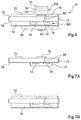
- the figure 6 represents another embodiment (not included in the invention) of an electronic device 70.
- the support 12 comprises two opposite faces 72, 74.
- the photodiode PH is made on the side of the face 72 while that the transistor M1 is formed on the side of the face 74.
- the electronic device 70 comprises a conductive portion 76 on the face 72 forming the cathode of the photodiode PH.
- the interface layer 32 covers the electrode 76 and the face 72.
- the remainder of the photodiode PH has the same structure as that described previously in relation to the figure 4 or 5 .
- An advantage of the device 70 is that it has a smaller footprint compared to the devices 10, 50 and 60.
- the transistor M1 can be better protected from light, in particular by the support 12 and the electrode 42.
- the drain and source electrodes 14, 16 of the transistor M1 are formed on the face 74.
- the semiconductor portion 18 covers the electrodes 14, 16 and extends on the face 74 between the electrodes 14, 16.
- a layer 78 same material as the interface layer 32, covers the electrodes 14, 16 and the semiconductor portion 18.
- the dielectric layer 40 covers the layer 78 and the gate electrode 42 of the transistor M1 is formed on the dielectric layer 40.
- the electrode 16 of the transistor M1 is connected to the electrode 76 of the photodiode PH by a conductive via 80 passing through the support 12.
- the Figures 7A and 7B illustrate steps of an embodiment of a method of manufacturing the electronic device 70.
- the Figure 7A represents the structure obtained after forming the via 80 through the support 12, the electrode 76 on the face 72 and the electrodes 14, 16 on the face 74 and after forming the semiconductor portion 18 on the face 74 of the support 12.
- the Figure 7B represents the structure obtained after plunging the structure represented in Figure 7A in a bath of the material forming the interface layer 32, which is for example in the form of a sol-gel, after removing the structure of the bath and after drying the structure.
- the layers 32 and 78 are then obtained.
- Subsequent steps of the method include forming the remaining layers of the photodiode PH and the remaining layers of the transistor M1.
Landscapes
- Engineering & Computer Science (AREA)
- Microelectronics & Electronic Packaging (AREA)
- Physics & Mathematics (AREA)
- Geometry (AREA)
- Thin Film Transistor (AREA)
- Junction Field-Effect Transistors (AREA)
Claims (12)
- Elektronische Vorrichtung (10) die Folgendes aufweist wenigstens eine optoelektronischen Komponente (PH), mit einer erste aktiven Schicht (30), einer ersten Elektrode (14) und einer zweiten Grenzflächenschicht (32) zwischen der ersten Schicht und der ersten Elektrode und wenigstens einen ersten Feldeffekttransistor (M1) mit einem ersten Halbleiterabschnitt (18) und einem ersten Gate (42) und mindestens einer dritten Schicht (33) zwischen dem ersten Gate und dem ersten Halbleiterabschnitt, wobei die dritte Schicht aus dem gleichen Material wie die zweite Schicht besteht, dadurch gekennzeichnet, dass die elektronische Vorrichtung eine zweite Elektrode (36) und eine vierte Schnittstellenschicht (34) zwischen der ersten Schicht (30) und der zweiten Elektrode aufweist sowie einen zweiten Feldeffekttransistor (M2) mit einem zweiten Halbleiterabschnitt (24), einem zweiten Gate (44) und wenigstens einer fünfte Schicht (35) zwischen dem zweiten Gate und dem zweiten Halbleiterabschnitt, wobei die fünfte Schicht aus dem gleichen Material wie die vierte Schicht besteht.
- Elektronische Vorrichtung nach Anspruch 1, ferner aufweisend eine vierte dielektrische Schicht (40), die zwischen der dritten Schicht (33) und dem ersten Gate (42) angeordnet ist.
- Elektronische Vorrichtung nach Anspruch 1 oder 2, wobei die dritte Schicht (33) ein Material aufweist, aus den Folgenden ausgewählt ist: Zinkoxid, Titanoxid, Cäsiumcarbonat oder einer Mischung aus wenigstens zwei dieser Verbindungen, wobei der elektrische Widerstand der dritten Schicht (33) größer oder gleich 109 Ω/□ ist.
- Elektronische Vorrichtung nach einem der Ansprüche 1 bis 3, wobei die Dicke der dritten Schicht (33) im Bereich von 0,1 nm bis 500 nm liegt.
- Elektronische Vorrichtung nach einem der Ansprüche 1 bis 4, wobei die erste Schicht (30) wenigstens ein erstes organisches Material aufweist.
- Elektronische Vorrichtung nach einem der Ansprüche 1 bis 5, wobei der erste Halbleiterabschnitt (18) ein zweites organisches Material aufweist.
- Elektronische Vorrichtung nach einem der Ansprüche 1 bis 6, wobei die zweite Schicht (32) ein Material umfasst, das den Folgenden ausgewählt ist: Zinkoxid, Titanoxid, Cäsiumcarbonat oder einer Mischung aus wenigstens zwei dieser Verbindungen.
- Elektronische Vorrichtung nach einem der Ansprüche 1 bis 7, wobei die dritte Schicht (33) eine Verlängerung der zweiten Schicht (32) ist.
- Elektronische Vorrichtung nach einem der Ansprüche 1 bis 8, wobei die fünfte Schicht (35) eine Verlängerung der vierten Schicht (34) ist.
- Elektronische Vorrichtung nach einem der Ansprüche 1 bis 9, wobei der erste Transistor (M1) vom N-Typ und der zweite Transistor (M2) vom P-Typ ist.
- Elektronische Vorrichtung nach einem der Ansprüche 1 bis 10, aufweisend einen Träger (12), wobei das erste Gate (42) auf einer Oberfläche des Trägers aufliegt.
- Elektronische Vorrichtung nach einem der Ansprüche 1 bis 11, aufweisend einen Träger (12) mit ersten und zweiten gegenüberliegenden Oberflächen (72, 74), wobei die optoelektronische Komponente (PH) auf der Seite der ersten Oberfläche (72) und der erste Transistor (M1) auf der Seite der zweiten Oberfläche (74) angeordnet ist.
Applications Claiming Priority (2)
| Application Number | Priority Date | Filing Date | Title |
|---|---|---|---|
| FR1451508A FR3017994B1 (fr) | 2014-02-25 | 2014-02-25 | Dispositif electronique comprenant un composant opto-electronique et un transistor organiques |
| PCT/EP2015/053938 WO2015128380A1 (fr) | 2014-02-25 | 2015-02-25 | Dispositif electronique comprenant un composant opto-electronique et un transistor organiques |
Publications (2)
| Publication Number | Publication Date |
|---|---|
| EP3111480A1 EP3111480A1 (de) | 2017-01-04 |
| EP3111480B1 true EP3111480B1 (de) | 2019-09-18 |
Family
ID=51205499
Family Applications (1)
| Application Number | Title | Priority Date | Filing Date |
|---|---|---|---|
| EP15706042.7A Active EP3111480B1 (de) | 2014-02-25 | 2015-02-25 | Elektronische vorrichtung mit organischer optoelektronischer komponente und zwei organischen transistoren |
Country Status (4)
| Country | Link |
|---|---|
| US (1) | US9761653B2 (de) |
| EP (1) | EP3111480B1 (de) |
| FR (1) | FR3017994B1 (de) |
| WO (1) | WO2015128380A1 (de) |
Families Citing this family (2)
| Publication number | Priority date | Publication date | Assignee | Title |
|---|---|---|---|---|
| CN107644937B (zh) * | 2016-07-22 | 2021-06-15 | 元太科技工业股份有限公司 | 电子组件封装体 |
| FR3098821B1 (fr) | 2019-07-19 | 2023-05-26 | Isorg | Encre pour une couche d’injection d’électrons |
Family Cites Families (6)
| Publication number | Priority date | Publication date | Assignee | Title |
|---|---|---|---|---|
| TW554525B (en) * | 2002-08-28 | 2003-09-21 | Ind Tech Res Inst | Organic integration device of thin film transistor and light emitting diode |
| US7732248B2 (en) * | 2004-08-31 | 2010-06-08 | Semiconductor Energy Laboratory Co., Ltd. | Manufacturing method of semiconductor device |
| GB0424468D0 (en) * | 2004-11-05 | 2004-12-08 | Elam T Ltd | Electroluminescent complexes |
| TWI248212B (en) * | 2004-12-06 | 2006-01-21 | Ritdisplay Corp | Organic electroluminescent device, pixel structure, array and driving method thereof |
| US8283655B2 (en) * | 2007-12-20 | 2012-10-09 | Palo Alto Research Center Incorporated | Producing layered structures with semiconductive regions or subregions |
| US20120169682A1 (en) * | 2010-12-29 | 2012-07-05 | Delphi Technologies, Inc. | Organic light emitting diode display device having a two-sided substrate and method of forming the same |
-
2014
- 2014-02-25 FR FR1451508A patent/FR3017994B1/fr not_active Expired - Fee Related
-
2015
- 2015-02-25 EP EP15706042.7A patent/EP3111480B1/de active Active
- 2015-02-25 US US15/121,584 patent/US9761653B2/en active Active
- 2015-02-25 WO PCT/EP2015/053938 patent/WO2015128380A1/fr active Application Filing
Non-Patent Citations (1)
| Title |
|---|
| None * |
Also Published As
| Publication number | Publication date |
|---|---|
| US9761653B2 (en) | 2017-09-12 |
| FR3017994A1 (fr) | 2015-08-28 |
| US20160365403A1 (en) | 2016-12-15 |
| WO2015128380A1 (fr) | 2015-09-03 |
| FR3017994B1 (fr) | 2017-09-01 |
| EP3111480A1 (de) | 2017-01-04 |
Similar Documents
| Publication | Publication Date | Title |
|---|---|---|
| FR3063564A1 (fr) | Capteur d'empreintes digitales integre dans un ecran d'affichage | |
| US10163374B2 (en) | Display unit and electronic apparatus | |
| EP3613080B1 (de) | Strahlungsdetektionsvorrichtung, organische fotodioden umfassend | |
| EP3550625B1 (de) | Verfahren zur herstellung einer stapelanordnung vom typ erste elektrode / aktive schicht / zweite elektrode | |
| EP3394893B1 (de) | Optoelektronische matrixanordnung mit transparenter oberer elektrode | |
| EP3111480B1 (de) | Elektronische vorrichtung mit organischer optoelektronischer komponente und zwei organischen transistoren | |
| WO2021043707A1 (fr) | Pixel d'ecran d'affichage | |
| EP3031087B1 (de) | Verfahren zur herstellung einer organischen cmos-schaltung und organische cmos-schaltung mit schutz vor uv-strahlung | |
| WO2019234339A1 (fr) | Dispositif optoelectronique et son procede de fabrication | |
| EP3622566A1 (de) | Elektronische vorrichtung mit verbesserter alterungsbeständigkeit | |
| WO2018108540A1 (fr) | Procede de formation d'un empilement et empilement | |
| EP4000110A1 (de) | Optoelektronische vorrichtung mit einer aktiven organischen schicht mit verbesserter leistung und verfahren zur herstellung dieser vorrichtung | |
| FR3091034A1 (fr) | Dispositif électronique à courant de fuite réduit | |
| EP2756532A1 (de) | Feldeffekttransistor mit einem leckstrombegrenzer |
Legal Events
| Date | Code | Title | Description |
|---|---|---|---|
| PUAI | Public reference made under article 153(3) epc to a published international application that has entered the european phase |
Free format text: ORIGINAL CODE: 0009012 |
|
| STAA | Information on the status of an ep patent application or granted ep patent |
Free format text: STATUS: REQUEST FOR EXAMINATION WAS MADE |
|
| 17P | Request for examination filed |
Effective date: 20160824 |
|
| AK | Designated contracting states |
Kind code of ref document: A1 Designated state(s): AL AT BE BG CH CY CZ DE DK EE ES FI FR GB GR HR HU IE IS IT LI LT LU LV MC MK MT NL NO PL PT RO RS SE SI SK SM TR |
|
| AX | Request for extension of the european patent |
Extension state: BA ME |
|
| RIN1 | Information on inventor provided before grant (corrected) |
Inventor name: VERILHAC, JEAN-MARIE Inventor name: BENWADIH, MOHAMMED |
|
| DAX | Request for extension of the european patent (deleted) | ||
| GRAP | Despatch of communication of intention to grant a patent |
Free format text: ORIGINAL CODE: EPIDOSNIGR1 |
|
| STAA | Information on the status of an ep patent application or granted ep patent |
Free format text: STATUS: GRANT OF PATENT IS INTENDED |
|
| INTG | Intention to grant announced |
Effective date: 20190605 |
|
| GRAS | Grant fee paid |
Free format text: ORIGINAL CODE: EPIDOSNIGR3 |
|
| GRAA | (expected) grant |
Free format text: ORIGINAL CODE: 0009210 |
|
| STAA | Information on the status of an ep patent application or granted ep patent |
Free format text: STATUS: THE PATENT HAS BEEN GRANTED |
|
| AK | Designated contracting states |
Kind code of ref document: B1 Designated state(s): AL AT BE BG CH CY CZ DE DK EE ES FI FR GB GR HR HU IE IS IT LI LT LU LV MC MK MT NL NO PL PT RO RS SE SI SK SM TR |
|
| REG | Reference to a national code |
Ref country code: GB Ref legal event code: FG4D Free format text: NOT ENGLISH |
|
| REG | Reference to a national code |
Ref country code: CH Ref legal event code: EP |
|
| REG | Reference to a national code |
Ref country code: DE Ref legal event code: R096 Ref document number: 602015038174 Country of ref document: DE |
|
| REG | Reference to a national code |
Ref country code: AT Ref legal event code: REF Ref document number: 1182325 Country of ref document: AT Kind code of ref document: T Effective date: 20191015 |
|
| REG | Reference to a national code |
Ref country code: IE Ref legal event code: FG4D Free format text: LANGUAGE OF EP DOCUMENT: FRENCH |
|
| REG | Reference to a national code |
Ref country code: NL Ref legal event code: MP Effective date: 20190918 |
|
| PG25 | Lapsed in a contracting state [announced via postgrant information from national office to epo] |
Ref country code: NO Free format text: LAPSE BECAUSE OF FAILURE TO SUBMIT A TRANSLATION OF THE DESCRIPTION OR TO PAY THE FEE WITHIN THE PRESCRIBED TIME-LIMIT Effective date: 20191218 Ref country code: BG Free format text: LAPSE BECAUSE OF FAILURE TO SUBMIT A TRANSLATION OF THE DESCRIPTION OR TO PAY THE FEE WITHIN THE PRESCRIBED TIME-LIMIT Effective date: 20191218 Ref country code: FI Free format text: LAPSE BECAUSE OF FAILURE TO SUBMIT A TRANSLATION OF THE DESCRIPTION OR TO PAY THE FEE WITHIN THE PRESCRIBED TIME-LIMIT Effective date: 20190918 Ref country code: LT Free format text: LAPSE BECAUSE OF FAILURE TO SUBMIT A TRANSLATION OF THE DESCRIPTION OR TO PAY THE FEE WITHIN THE PRESCRIBED TIME-LIMIT Effective date: 20190918 Ref country code: HR Free format text: LAPSE BECAUSE OF FAILURE TO SUBMIT A TRANSLATION OF THE DESCRIPTION OR TO PAY THE FEE WITHIN THE PRESCRIBED TIME-LIMIT Effective date: 20190918 Ref country code: SE Free format text: LAPSE BECAUSE OF FAILURE TO SUBMIT A TRANSLATION OF THE DESCRIPTION OR TO PAY THE FEE WITHIN THE PRESCRIBED TIME-LIMIT Effective date: 20190918 |
|
| REG | Reference to a national code |
Ref country code: LT Ref legal event code: MG4D |
|
| PG25 | Lapsed in a contracting state [announced via postgrant information from national office to epo] |
Ref country code: AL Free format text: LAPSE BECAUSE OF FAILURE TO SUBMIT A TRANSLATION OF THE DESCRIPTION OR TO PAY THE FEE WITHIN THE PRESCRIBED TIME-LIMIT Effective date: 20190918 Ref country code: RS Free format text: LAPSE BECAUSE OF FAILURE TO SUBMIT A TRANSLATION OF THE DESCRIPTION OR TO PAY THE FEE WITHIN THE PRESCRIBED TIME-LIMIT Effective date: 20190918 Ref country code: GR Free format text: LAPSE BECAUSE OF FAILURE TO SUBMIT A TRANSLATION OF THE DESCRIPTION OR TO PAY THE FEE WITHIN THE PRESCRIBED TIME-LIMIT Effective date: 20191219 Ref country code: LV Free format text: LAPSE BECAUSE OF FAILURE TO SUBMIT A TRANSLATION OF THE DESCRIPTION OR TO PAY THE FEE WITHIN THE PRESCRIBED TIME-LIMIT Effective date: 20190918 |
|
| REG | Reference to a national code |
Ref country code: AT Ref legal event code: MK05 Ref document number: 1182325 Country of ref document: AT Kind code of ref document: T Effective date: 20190918 |
|
| PG25 | Lapsed in a contracting state [announced via postgrant information from national office to epo] |
Ref country code: IT Free format text: LAPSE BECAUSE OF FAILURE TO SUBMIT A TRANSLATION OF THE DESCRIPTION OR TO PAY THE FEE WITHIN THE PRESCRIBED TIME-LIMIT Effective date: 20190918 Ref country code: PT Free format text: LAPSE BECAUSE OF FAILURE TO SUBMIT A TRANSLATION OF THE DESCRIPTION OR TO PAY THE FEE WITHIN THE PRESCRIBED TIME-LIMIT Effective date: 20200120 Ref country code: PL Free format text: LAPSE BECAUSE OF FAILURE TO SUBMIT A TRANSLATION OF THE DESCRIPTION OR TO PAY THE FEE WITHIN THE PRESCRIBED TIME-LIMIT Effective date: 20190918 Ref country code: EE Free format text: LAPSE BECAUSE OF FAILURE TO SUBMIT A TRANSLATION OF THE DESCRIPTION OR TO PAY THE FEE WITHIN THE PRESCRIBED TIME-LIMIT Effective date: 20190918 Ref country code: AT Free format text: LAPSE BECAUSE OF FAILURE TO SUBMIT A TRANSLATION OF THE DESCRIPTION OR TO PAY THE FEE WITHIN THE PRESCRIBED TIME-LIMIT Effective date: 20190918 Ref country code: RO Free format text: LAPSE BECAUSE OF FAILURE TO SUBMIT A TRANSLATION OF THE DESCRIPTION OR TO PAY THE FEE WITHIN THE PRESCRIBED TIME-LIMIT Effective date: 20190918 Ref country code: NL Free format text: LAPSE BECAUSE OF FAILURE TO SUBMIT A TRANSLATION OF THE DESCRIPTION OR TO PAY THE FEE WITHIN THE PRESCRIBED TIME-LIMIT Effective date: 20190918 Ref country code: ES Free format text: LAPSE BECAUSE OF FAILURE TO SUBMIT A TRANSLATION OF THE DESCRIPTION OR TO PAY THE FEE WITHIN THE PRESCRIBED TIME-LIMIT Effective date: 20190918 |
|
| PG25 | Lapsed in a contracting state [announced via postgrant information from national office to epo] |
Ref country code: IS Free format text: LAPSE BECAUSE OF FAILURE TO SUBMIT A TRANSLATION OF THE DESCRIPTION OR TO PAY THE FEE WITHIN THE PRESCRIBED TIME-LIMIT Effective date: 20200224 Ref country code: CZ Free format text: LAPSE BECAUSE OF FAILURE TO SUBMIT A TRANSLATION OF THE DESCRIPTION OR TO PAY THE FEE WITHIN THE PRESCRIBED TIME-LIMIT Effective date: 20190918 Ref country code: SK Free format text: LAPSE BECAUSE OF FAILURE TO SUBMIT A TRANSLATION OF THE DESCRIPTION OR TO PAY THE FEE WITHIN THE PRESCRIBED TIME-LIMIT Effective date: 20190918 Ref country code: SM Free format text: LAPSE BECAUSE OF FAILURE TO SUBMIT A TRANSLATION OF THE DESCRIPTION OR TO PAY THE FEE WITHIN THE PRESCRIBED TIME-LIMIT Effective date: 20190918 |
|
| REG | Reference to a national code |
Ref country code: DE Ref legal event code: R097 Ref document number: 602015038174 Country of ref document: DE |
|
| PLBE | No opposition filed within time limit |
Free format text: ORIGINAL CODE: 0009261 |
|
| STAA | Information on the status of an ep patent application or granted ep patent |
Free format text: STATUS: NO OPPOSITION FILED WITHIN TIME LIMIT |
|
| PG2D | Information on lapse in contracting state deleted |
Ref country code: IS |
|
| PG25 | Lapsed in a contracting state [announced via postgrant information from national office to epo] |
Ref country code: DK Free format text: LAPSE BECAUSE OF FAILURE TO SUBMIT A TRANSLATION OF THE DESCRIPTION OR TO PAY THE FEE WITHIN THE PRESCRIBED TIME-LIMIT Effective date: 20190918 Ref country code: IS Free format text: LAPSE BECAUSE OF FAILURE TO SUBMIT A TRANSLATION OF THE DESCRIPTION OR TO PAY THE FEE WITHIN THE PRESCRIBED TIME-LIMIT Effective date: 20200119 |
|
| 26N | No opposition filed |
Effective date: 20200619 |
|
| PG25 | Lapsed in a contracting state [announced via postgrant information from national office to epo] |
Ref country code: SI Free format text: LAPSE BECAUSE OF FAILURE TO SUBMIT A TRANSLATION OF THE DESCRIPTION OR TO PAY THE FEE WITHIN THE PRESCRIBED TIME-LIMIT Effective date: 20190918 |
|
| REG | Reference to a national code |
Ref country code: CH Ref legal event code: PL |
|
| REG | Reference to a national code |
Ref country code: BE Ref legal event code: MM Effective date: 20200229 |
|
| PG25 | Lapsed in a contracting state [announced via postgrant information from national office to epo] |
Ref country code: LU Free format text: LAPSE BECAUSE OF NON-PAYMENT OF DUE FEES Effective date: 20200225 Ref country code: MC Free format text: LAPSE BECAUSE OF FAILURE TO SUBMIT A TRANSLATION OF THE DESCRIPTION OR TO PAY THE FEE WITHIN THE PRESCRIBED TIME-LIMIT Effective date: 20190918 |
|
| PG25 | Lapsed in a contracting state [announced via postgrant information from national office to epo] |
Ref country code: CH Free format text: LAPSE BECAUSE OF NON-PAYMENT OF DUE FEES Effective date: 20200229 Ref country code: LI Free format text: LAPSE BECAUSE OF NON-PAYMENT OF DUE FEES Effective date: 20200229 |
|
| PG25 | Lapsed in a contracting state [announced via postgrant information from national office to epo] |
Ref country code: IE Free format text: LAPSE BECAUSE OF NON-PAYMENT OF DUE FEES Effective date: 20200225 |
|
| PG25 | Lapsed in a contracting state [announced via postgrant information from national office to epo] |
Ref country code: BE Free format text: LAPSE BECAUSE OF NON-PAYMENT OF DUE FEES Effective date: 20200229 |
|
| PGFP | Annual fee paid to national office [announced via postgrant information from national office to epo] |
Ref country code: FR Payment date: 20210226 Year of fee payment: 7 |
|
| PGFP | Annual fee paid to national office [announced via postgrant information from national office to epo] |
Ref country code: DE Payment date: 20210209 Year of fee payment: 7 Ref country code: GB Payment date: 20210216 Year of fee payment: 7 |
|
| PG25 | Lapsed in a contracting state [announced via postgrant information from national office to epo] |
Ref country code: TR Free format text: LAPSE BECAUSE OF FAILURE TO SUBMIT A TRANSLATION OF THE DESCRIPTION OR TO PAY THE FEE WITHIN THE PRESCRIBED TIME-LIMIT Effective date: 20190918 Ref country code: MT Free format text: LAPSE BECAUSE OF FAILURE TO SUBMIT A TRANSLATION OF THE DESCRIPTION OR TO PAY THE FEE WITHIN THE PRESCRIBED TIME-LIMIT Effective date: 20190918 Ref country code: CY Free format text: LAPSE BECAUSE OF FAILURE TO SUBMIT A TRANSLATION OF THE DESCRIPTION OR TO PAY THE FEE WITHIN THE PRESCRIBED TIME-LIMIT Effective date: 20190918 |
|
| PG25 | Lapsed in a contracting state [announced via postgrant information from national office to epo] |
Ref country code: MK Free format text: LAPSE BECAUSE OF FAILURE TO SUBMIT A TRANSLATION OF THE DESCRIPTION OR TO PAY THE FEE WITHIN THE PRESCRIBED TIME-LIMIT Effective date: 20190918 |
|
| REG | Reference to a national code |
Ref country code: DE Ref legal event code: R119 Ref document number: 602015038174 Country of ref document: DE |
|
| GBPC | Gb: european patent ceased through non-payment of renewal fee |
Effective date: 20220225 |
|
| PG25 | Lapsed in a contracting state [announced via postgrant information from national office to epo] |
Ref country code: FR Free format text: LAPSE BECAUSE OF NON-PAYMENT OF DUE FEES Effective date: 20220228 |
|
| PG25 | Lapsed in a contracting state [announced via postgrant information from national office to epo] |
Ref country code: GB Free format text: LAPSE BECAUSE OF NON-PAYMENT OF DUE FEES Effective date: 20220225 Ref country code: DE Free format text: LAPSE BECAUSE OF NON-PAYMENT OF DUE FEES Effective date: 20220901 |