EP3608900A1 - Led driving circuits - Google Patents
Led driving circuits Download PDFInfo
- Publication number
- EP3608900A1 EP3608900A1 EP19186837.1A EP19186837A EP3608900A1 EP 3608900 A1 EP3608900 A1 EP 3608900A1 EP 19186837 A EP19186837 A EP 19186837A EP 3608900 A1 EP3608900 A1 EP 3608900A1
- Authority
- EP
- European Patent Office
- Prior art keywords
- transistor
- latch
- signal
- bit
- node
- Prior art date
- Legal status (The legal status is an assumption and is not a legal conclusion. Google has not performed a legal analysis and makes no representation as to the accuracy of the status listed.)
- Granted
Links
Images








Classifications
-
- G—PHYSICS
- G09—EDUCATION; CRYPTOGRAPHY; DISPLAY; ADVERTISING; SEALS
- G09G—ARRANGEMENTS OR CIRCUITS FOR CONTROL OF INDICATING DEVICES USING STATIC MEANS TO PRESENT VARIABLE INFORMATION
- G09G3/00—Control arrangements or circuits, of interest only in connection with visual indicators other than cathode-ray tubes
- G09G3/20—Control arrangements or circuits, of interest only in connection with visual indicators other than cathode-ray tubes for presentation of an assembly of a number of characters, e.g. a page, by composing the assembly by combination of individual elements arranged in a matrix no fixed position being assigned to or needed to be assigned to the individual characters or partial characters
- G09G3/22—Control arrangements or circuits, of interest only in connection with visual indicators other than cathode-ray tubes for presentation of an assembly of a number of characters, e.g. a page, by composing the assembly by combination of individual elements arranged in a matrix no fixed position being assigned to or needed to be assigned to the individual characters or partial characters using controlled light sources
- G09G3/30—Control arrangements or circuits, of interest only in connection with visual indicators other than cathode-ray tubes for presentation of an assembly of a number of characters, e.g. a page, by composing the assembly by combination of individual elements arranged in a matrix no fixed position being assigned to or needed to be assigned to the individual characters or partial characters using controlled light sources using electroluminescent panels
- G09G3/32—Control arrangements or circuits, of interest only in connection with visual indicators other than cathode-ray tubes for presentation of an assembly of a number of characters, e.g. a page, by composing the assembly by combination of individual elements arranged in a matrix no fixed position being assigned to or needed to be assigned to the individual characters or partial characters using controlled light sources using electroluminescent panels semiconductive, e.g. using light-emitting diodes [LED]
-
- G—PHYSICS
- G09—EDUCATION; CRYPTOGRAPHY; DISPLAY; ADVERTISING; SEALS
- G09G—ARRANGEMENTS OR CIRCUITS FOR CONTROL OF INDICATING DEVICES USING STATIC MEANS TO PRESENT VARIABLE INFORMATION
- G09G3/00—Control arrangements or circuits, of interest only in connection with visual indicators other than cathode-ray tubes
- G09G3/20—Control arrangements or circuits, of interest only in connection with visual indicators other than cathode-ray tubes for presentation of an assembly of a number of characters, e.g. a page, by composing the assembly by combination of individual elements arranged in a matrix no fixed position being assigned to or needed to be assigned to the individual characters or partial characters
- G09G3/2007—Display of intermediate tones
- G09G3/2014—Display of intermediate tones by modulation of the duration of a single pulse during which the logic level remains constant
-
- G—PHYSICS
- G09—EDUCATION; CRYPTOGRAPHY; DISPLAY; ADVERTISING; SEALS
- G09G—ARRANGEMENTS OR CIRCUITS FOR CONTROL OF INDICATING DEVICES USING STATIC MEANS TO PRESENT VARIABLE INFORMATION
- G09G3/00—Control arrangements or circuits, of interest only in connection with visual indicators other than cathode-ray tubes
- G09G3/20—Control arrangements or circuits, of interest only in connection with visual indicators other than cathode-ray tubes for presentation of an assembly of a number of characters, e.g. a page, by composing the assembly by combination of individual elements arranged in a matrix no fixed position being assigned to or needed to be assigned to the individual characters or partial characters
- G09G3/34—Control arrangements or circuits, of interest only in connection with visual indicators other than cathode-ray tubes for presentation of an assembly of a number of characters, e.g. a page, by composing the assembly by combination of individual elements arranged in a matrix no fixed position being assigned to or needed to be assigned to the individual characters or partial characters by control of light from an independent source
- G09G3/3406—Control of illumination source
-
- H—ELECTRICITY
- H05—ELECTRIC TECHNIQUES NOT OTHERWISE PROVIDED FOR
- H05B—ELECTRIC HEATING; ELECTRIC LIGHT SOURCES NOT OTHERWISE PROVIDED FOR; CIRCUIT ARRANGEMENTS FOR ELECTRIC LIGHT SOURCES, IN GENERAL
- H05B45/00—Circuit arrangements for operating light-emitting diodes [LED]
- H05B45/10—Controlling the intensity of the light
-
- H—ELECTRICITY
- H05—ELECTRIC TECHNIQUES NOT OTHERWISE PROVIDED FOR
- H05B—ELECTRIC HEATING; ELECTRIC LIGHT SOURCES NOT OTHERWISE PROVIDED FOR; CIRCUIT ARRANGEMENTS FOR ELECTRIC LIGHT SOURCES, IN GENERAL
- H05B45/00—Circuit arrangements for operating light-emitting diodes [LED]
- H05B45/30—Driver circuits
- H05B45/37—Converter circuits
- H05B45/3725—Switched mode power supply [SMPS]
- H05B45/39—Circuits containing inverter bridges
-
- G—PHYSICS
- G09—EDUCATION; CRYPTOGRAPHY; DISPLAY; ADVERTISING; SEALS
- G09G—ARRANGEMENTS OR CIRCUITS FOR CONTROL OF INDICATING DEVICES USING STATIC MEANS TO PRESENT VARIABLE INFORMATION
- G09G2230/00—Details of flat display driving waveforms
-
- G—PHYSICS
- G09—EDUCATION; CRYPTOGRAPHY; DISPLAY; ADVERTISING; SEALS
- G09G—ARRANGEMENTS OR CIRCUITS FOR CONTROL OF INDICATING DEVICES USING STATIC MEANS TO PRESENT VARIABLE INFORMATION
- G09G2300/00—Aspects of the constitution of display devices
- G09G2300/04—Structural and physical details of display devices
- G09G2300/0439—Pixel structures
-
- G—PHYSICS
- G09—EDUCATION; CRYPTOGRAPHY; DISPLAY; ADVERTISING; SEALS
- G09G—ARRANGEMENTS OR CIRCUITS FOR CONTROL OF INDICATING DEVICES USING STATIC MEANS TO PRESENT VARIABLE INFORMATION
- G09G2310/00—Command of the display device
- G09G2310/02—Addressing, scanning or driving the display screen or processing steps related thereto
- G09G2310/0243—Details of the generation of driving signals
-
- G—PHYSICS
- G09—EDUCATION; CRYPTOGRAPHY; DISPLAY; ADVERTISING; SEALS
- G09G—ARRANGEMENTS OR CIRCUITS FOR CONTROL OF INDICATING DEVICES USING STATIC MEANS TO PRESENT VARIABLE INFORMATION
- G09G2310/00—Command of the display device
- G09G2310/02—Addressing, scanning or driving the display screen or processing steps related thereto
- G09G2310/0243—Details of the generation of driving signals
- G09G2310/0245—Clearing or presetting the whole screen independently of waveforms, e.g. on power-on
-
- G—PHYSICS
- G09—EDUCATION; CRYPTOGRAPHY; DISPLAY; ADVERTISING; SEALS
- G09G—ARRANGEMENTS OR CIRCUITS FOR CONTROL OF INDICATING DEVICES USING STATIC MEANS TO PRESENT VARIABLE INFORMATION
- G09G2310/00—Command of the display device
- G09G2310/06—Details of flat display driving waveforms
-
- G—PHYSICS
- G09—EDUCATION; CRYPTOGRAPHY; DISPLAY; ADVERTISING; SEALS
- G09G—ARRANGEMENTS OR CIRCUITS FOR CONTROL OF INDICATING DEVICES USING STATIC MEANS TO PRESENT VARIABLE INFORMATION
- G09G2320/00—Control of display operating conditions
- G09G2320/06—Adjustment of display parameters
- G09G2320/0626—Adjustment of display parameters for control of overall brightness
-
- G—PHYSICS
- G09—EDUCATION; CRYPTOGRAPHY; DISPLAY; ADVERTISING; SEALS
- G09G—ARRANGEMENTS OR CIRCUITS FOR CONTROL OF INDICATING DEVICES USING STATIC MEANS TO PRESENT VARIABLE INFORMATION
- G09G2320/00—Control of display operating conditions
- G09G2320/06—Adjustment of display parameters
- G09G2320/0626—Adjustment of display parameters for control of overall brightness
- G09G2320/064—Adjustment of display parameters for control of overall brightness by time modulation of the brightness of the illumination source
Definitions
- the disclosure relates generally to circuits for driving LED units, and more particularly it relates to circuits for dimming with pulse-width modulation (PWM).
- PWM pulse-width modulation
- Active matrix LED display/backlight with mini- and micro-LED and OLED equips a current driver to control the luminance of LED units in each pixel.
- the driver is serially connected to the LED between two voltage sources in order to control the current of the LED for luminance adjustment.
- PWM Pulse Width Modulation
- an LED driving circuit for illuminating a first LED unit.
- the LED driving circuit comprises: a data latch circuit, a current source, and a PWM circuit.
- the data latch circuit latches a data signal according to a first latch signal to generate a first control signal.
- the current source generates a constant current.
- the PWM circuit periodically passes the constant current through the first LED unit according to the first control signal and an enable signal.
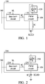
- Fig. 1 is a block diagram of an LED driving circuit in accordance with an embodiment of the disclosure.
- the LED driving circuit 100 is configured to illuminate the LED unit XLED, which includes a data latch circuit 110, a current source 120, and a PWM circuit 130.
- the LED driving circuit 100 may comprise a plurality of transistors implemented by P-type transistors. According to another embodiment of the disclosure, the LED driving circuit 100 may comprise a plurality of transistors implemented by N-type transistors. In other words, the LED driving circuit 100 may comprise a plurality of transistors implemented by either P-type transistors or N-type transistors.
- the data latch circuit 110 latches the data signal SD according to a latch signal SL to generate the control signal SC.
- the current source 120 generates a constant current IC.
- the PWM circuit 130 periodically passes the constant current IC according to the control signal SC and the enable signal EN so that the constant current IC flows through the LED unit XLED. As shown in Fig. 1 , whether the current source 120 sinks or sources the constant current IC is based on whether the LED driving circuit 100 is implemented by P-type transistors or N-type transistors.
- Fig. 2 is a block diagram of an LED driving circuit in accordance with an embodiment of the disclosure, in which the LED driving circuit in Fig. 2 comprises a plurality of transistors implemented by P-type transistors.
- the LED driving circuit 200 includes a data latch circuit 210, a current source 220, and a PWM circuit 230, in which the data latch circuit 210, the current source 220, and the PWM circuit 230 correspond to the data latch circuit 110, the current source 120, and the PWM circuit 130 in Fig. 1 .
- the LED driving circuit 200 couples the constant current IC to the LED unit XLED so that the constant current IC flows through the LED unit XLED to the ground.
- Fig. 3 is a block diagram of an LED driving circuit in accordance with another embodiment of the disclosure, in which the LED driving circuit in Fig. 3 comprises a plurality of transistors implemented by N-type transistors.
- the LED driving circuit 300 includes a data latch circuit 310, a current source 320, and a PWM circuit 330, in which the data latch circuit 310, the current source 320, and the PWM circuit 330 correspond to the data latch circuit 110, the current source 120, and the PWM circuit 130 in Fig. 1 .
- the LED driving circuit 300 couples the constant current IC to the LED unit XLED so that the constant current IC flows through the LED unit XLED from the supply voltage VDD.
- the data signal SD, the control signal SC, and the enable signal EN are N bits, in which N is a positive integer.
- N-type transistors and P-type transistors are complementary, one skilled in the art will understand how to modify the embodiments of the LED driving circuit with P-type transistors provided as follows to obtain the LED driving circuit with N-type transistors. In the following paragraphs, the LED driving circuit with P-type transistors are illustrated, but not intended to be limited to the embodiments with P-type transistors.
- Fig. 4 is a block diagram of the PWM circuit 230 in Fig. 2 in accordance with an embodiment of the disclosure.
- the PWM circuit 400 includes a first transmission transistor 410, a second transmission transistor 420, a third transmission transistor 430, a fourth transmission transistor 440, a pull-up transistor 450, and a dimming transistor 460.
- the data signal SD, the control signal SC, and the enable signal EN are illustrated as 4-bit herein, but not intended to be limited thereto.
- the control signal SC includes a first bit BIT_1, a second bit BIT_2, a third bit BIT_3, and a fourth bit BIT_4, and the enable signal EN includes a first enable EN_1, a second enable EN_2, a third enable EN_3, and a fourth enable EN_4.
- the first transmission transistor 410, the second transmission transistor 420, the third transmission transistor 430, and the fourth transmission transistor 440 respectively pass the first bit BIT_1, the second bit BIT_2, the third bit BIT_3, and the fourth bit BIT_4 to a PWM signal SPWM according to the first enable EN_1, the second enable EN_2, the third enable EN_3, and the fourth enable EN_4.
- the duty cycles of the first enable EN_1, the second enable EN_2, the third enable EN_3, and the fourth enable EN_4 are 50%, 25%, 12.5%, and 6.25% respectively.
- the dimming transistor 460 is turned ON according to the PWM signal SPWM so that the constant current IC can flow through the LED unit XLED to illuminate the LED unit XLED.
- the pull-up transistor 450 pulls the PWM signal SPWM up to the supply voltage VDD to turn OFF the dimming transistor 460 when the first transmission transistor 410, the second transmission transistor 420, the third transmission transistor 430, and the fourth transmission transistor 440 are all turned OFF.
- the LED unit XLED in Fig. 4 is normally OFF, and the first bit BIT_1, the second bit BIT_2, the third bit BIT_3, and the fourth bit BIT_4 are configured to turn ON the LED unit XLED.
- the gate terminal of the pull-up transistor 450 is controlled by the PWM signal SPWM. Namely, the gate terminal of the pull-up transistor 450 is coupled to its drain terminal. According to other embodiments of the disclosure, the gate terminal of the pull-up transistor 450 may be controlled by another signal, such as the latch signal SL.
- the PWM circuit 400 may include a first pull-up transistor and a second pull-up transistor (not shown in Fig. 4 ) which are controlled by a first latch signal SL1 and a second latch signal SL2, in which the first latch signal SL1 is configured to drive the LED unit XLED in Fig. 4 , and the second latch signal SL2 is configured to drive another LED unit (not shown in Fig. 4 ).
- the first latch signal SL1 and the second latch signal SL2 will be described in the following paragraphs.
- the first transmission transistor 410, the second transmission transistor 420, the third transmission transistor 430, or the fourth transmission transistor 440 is turned ON by the first enable EN_1, the second enable EN_2, the third enable EN_3, or the fourth enable EN_4 at the low voltage level.
- the first transmission transistor 410, the second transmission transistor 420, the third transmission transistor 430, and the fourth transmission transistor 440 are active low.
- Fig. 5 is a block diagram of a latch unit in accordance with an embodiment of the disclosure.
- the data latch circuit 110 includes a plurality of latch units.
- the latch unit of the data latch circuit 110 is the latch unit 500 in Fig. 5 .
- the latch unit 500 generates a control bit CBIT which corresponds to any one of the first bit BIT_1, the second bit BIT_2, the third bit BIT_3, and the fourth bit BIT_4 of the control signal SC in Fig. 4 according to a corresponding data bit DB of the data signal SD.
- the latch unit 500 includes a first transistor M1, a first capacitor C1, a second transistor M2, a third transistor M3, a second capacitor C2, and a fourth transistor M4.
- the data signal SD includes a plurality of data bits DB, in which each data bit DB includes positive data DP and negative data DN, in which the negative data DN is an inverse of the positive data DP.
- the first transistor M1 provides the negative data DN from a data bit DB of the data signal SD to a first node N1 according to the latch signal SL.
- the first capacitor C1 which is coupled between the first node N1 and the ground, stores the negative data DN.
- the second transistor M2 couples a control bit CBIT of the control signal SC to the ground according to the negative data DN stored in the first capacitor C1.
- the control bit CBIT in Fig. 5 may be any one of the first bit BIT_1, the second bit BIT_2, the third bit BIT_3, and the fourth bit BIT 4 of the control signal SC in Fig. 4 .
- the negative data DN ranges from a low voltage level to a high voltage level, in which the low voltage level should be less than the ground by the absolute value of the threshold voltage of the second transistor M2 so that the second transistor M2 can be completely turned ON when the negative data DN is at the low voltage level.
- the third transistor M3 provides the positive data DP from the data bit DB of the data signal SD to a second node N2 according to the latch signal SL.
- the second capacitor C2 which is coupled between the second node N2 and the ground, stores the positive data DP.
- the fourth transistor M4 provides the supply voltage VDD to the control bit CBIT of the control signal SC according to the positive data DP at the second node N2.
- the first capacitor C1 and the second capacitor C2 are required to form a pair of memory units, and the second transistor M2 and the fourth transistor M4 form a complementary push-pull driver to generate the control bit CBIT of the control signal SD.
- Fig. 6 is a block diagram of a latch unit in accordance with another embodiment of the disclosure.
- the latch unit 600 includes the first transistor M1, the first capacitor C1, the second transistor M2 of Fig. 5 .
- a plurality of the latch units 600 are coupled to a corresponding one of the first bit BIT_1, the second bit BIT_2, the third bit BIT_3, and the fourth bit BIT_4 of the PWM circuit 60, and only one latch unit 600 is illustrated herein.
- the PWM circuit 60 includes a first transmission transistor 61, a second transmission transistor 62, a third transmission transistor 63, a fourth transmission transistor 64, a pull-up transistor 65, and a dimming transistor 66, which corresponds to the PWM circuit 400.
- the pull-up transistor 65 is required to normally turn OFF the dimming transistor 66 when the first transmission transistor 61, the second transmission transistor 62, the third transmission transistor 63, and the fourth transmission transistor 64 are all OFF.
- the low voltage level of the negative data DN should be less than the ground level by an absolute value of the threshold voltage of the second transistor M2.
- Fig. 7 is a block diagram of a latch unit in accordance with another embodiment of the disclosure.
- the latch unit 700 includes the third transistor M3, the second capacitor C2, and the fourth transistor M4.
- a plurality of the latch units 700 are coupled to a corresponding one of the first bit BIT_1, the second bit BIT_2, the third bit BIT_3, and the fourth bit BIT_4 of the PWM circuit 70, and only one latch unit 700 is illustrated herein.
- the PWM circuit 70 includes a first transmission transistor 71, a second transmission transistor 72, a third transmission transistor 73, a fourth transmission transistor 74, a pull-down transistor 75, and a dimming transistor 76, which corresponds to the PWM circuit 400 in Fig. 4 .
- the pull-down transistor 75 is required to normally turn ON the dimming transistor 76 when the first transmission transistor 71, the second transmission transistor 72, the third transmission transistor 73, and the fourth transmission transistor 74 are all OFF.
- the first enable EN_1, the second enable EN_2, the third enable EN_3, and the fourth enable EN_4 in Fig. 7 are allowed to overlap since each of the first bit BIT_1, the second bit BIT_2, the third bit BIT_3, and the fourth bit BIT_4 is high impedance in the high logic level.
- the pull-down transistor 75 pulls the PWM signal SPWM down to the ground.
- the gate terminal of the pull-down transistor 75 is tied to the ground.
- the gate terminal of the pull-down transistor 75 may be controlled by another signal, such as the latch signal SL.
- the pull-down transistor 75 is configured to normally pull the PWM signal SPWM down to the ground level when the first transmission transistor 71, the second transmission transistor 72, the third transmission transistor 73, and the fourth transmission transistor 74 are all OFF.
- the first enable EN_1, the second enable EN_2, the third enable EN_3, and the fourth enable EN_4 are overlapped since the control bit CBIT is in a high impedance state when the control bit CBIT is at the high voltage level.
- Fig. 8 is a block diagram of a latch unit in accordance with another embodiment of the disclosure. Comparing the latch unit 800 in Fig. 8 to the latch unit 500 in Fig. 5 , the latch unit 800 further includes a bootstrap transistor MBST and a bootstrap capacitor CBST.
- the bootstrap transistor MBST is coupled between the first node N1 and the gate terminal of the second transistor M2, and the gate terminal of the bootstrap transistor MBST is coupled to the ground.
- the bootstrap capacitor CBST is coupled between the control bit CBIT and the gate terminal of the second transistor M2.
- the low voltage level of the negative data DN can be as low as the ground level of the latch unit 800.
- the bootstrap transistor MBST and the bootstrap capacitor CBST are configured to completely turn ON the second transistor M2 so that the control bit CBIT can be pulled down to the ground.
- the effect of the bootstrap transistor MBST and the bootstrap capacitor CBST could be limited if the voltage difference between two terminals of the bootstrap capacitance CBST is small when the control bit CBIT is at the low voltage level before the latch signal SL turns ON the first transistor M1.
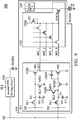
- Fig. 9 is a block diagram of an LED driving array in accordance with another embodiment of the disclosure.
- the LED driving array 900 includes a first LED driving circuit 910 and a second LED driving circuit 920.
- the LED driving array 900 may include a plurality of LED driving circuits.
- the LED driving array 900 including two LED driving circuits are illustrated herein, but not intended to be limited thereto.
- the first LED driving circuit 910 is configured to illuminate the first LED unit XLED1 according to the data signal SD and the first latch signal SL1
- the second LED driving circuit 920 is configured to illuminate the second LED unit XLED2 according to the data signal SD and the second latch signal SL2.
- the second LED unit XLED2 is illuminated prior to the first LED unit XLED1.
- the second latch signal SL2 is activated prior to the first latch signal SL1.
- the second LED unit XLED2 is placed near the first LED unit XLED1 and illuminated prior to the first LED unit XLED1.
- the second latch signal SL2 may be viewed as a latch signal prior to the first latch signal SL1.
- the first LED driving circuit 910 includes a plurality of latch units 911, each of which generates a corresponding bit of the control signal SC (i.e., the control bit CBIT) to the PWM circuit 912.
- the PWM circuit 912 corresponds to the PWM circuit 400 in Fig. 4 , which is not repeated herein.
- the PWM circuit includes a pull-up transistor PU.
- the pull-up transistor PU is controlled by the PWM signal SPWM. Namely, the gate terminal of the pull-up transistor PU is coupled to its drain terminal.
- the gate terminal of the pull-up transistor PU is controlled by the first latch signal SL1.
- the gate terminal of the pull-up transistor PU is controlled by the second latch signal SL2.
- the latch unit 911 further includes a first preset transistor MR1 and a second preset transistor MR2.
- the first preset transistor MR1 is configured to provide the supply voltage VDD to the first node N1 according to the second latch signal SL2.
- the second present transistor MR2 is configured to provide the ground to the second node N2 according to the second latch signal SL2.
- the second LED unit XLED2 is turned ON prior to the first LED unit XLED1.
- the second latch signal SL2 is also configured to turn ON the first preset transistor MR1 and the second preset transistor MR2 of the latch unit 911 in the first LED driving circuit 910 to preset the voltages of the control bit CBIT and the first node N1.
- the first preset transistor MR1 and the second preset transistor MR2 are turned ON, the voltage of the first node N1 is pulled up to the supply voltage VDD, and the voltage of the second node N2 is pull down to the ground level.
- the second transistor M2 is turned OFF and the fourth transistor M4 is turned ON so that the control bit CBIT is pulled up to the supply voltage VDD.
- the voltages of both terminals of the bootstrap capacitor CBST are preset to the supply voltage VDD by the second latch signal SL2.
- the voltage of the gate terminal of the second transistor M2 is equal to an absolute value of the threshold voltage of the bootstrap transistor MBST since the bootstrap transistor MBST is turned OFF.
- the bootstrap transistor MBST is configured to separate the first node N1 and the gate terminal of the second transistor M2 so that the gate terminal of the second transistor M2 can be better pulled down to a voltage lower than zero by AC coupling through the bootstrap capacitor CBST.
- the PWM circuit includes a pull-up transistor PU.
- the pull-up transistor PU is controlled by the PWM signal SPWM. Namely, the gate terminal of the pull-up transistor PU is coupled to its drain terminal.
- the gate terminal of the pull-up transistor PU is controlled by the first latch signal SL1 (not shown in Fig. 9 ).
- the gate terminal of the pull-up transistor PU is controlled by the second latch signal SL2 (not shown in Fig. 9 ).
- Fig. 10 is a block diagram of an LED driving array in accordance with another embodiment of the disclosure.
- the LED driving array 1000 includes a first LED driving circuit 1010 and a second LED driving circuit 1020.
- the LED driving array 1000 may include a plurality of LED driving circuits.
- the LED driving array 1000 including two LED driving circuits are illustrated herein, but not intended to be limited thereto.
- the first LED driving circuit 1010 is configured to illuminate the first LED unit XLED1 according to the data signal SD and the first latch signal SL1
- the second LED driving circuit 1020 is configured to illuminate the second LED unit XLED2 according to the data signal SD and the second latch signal SL2.
- the second LED unit XLED2 is illuminated prior to the first LED unit XLED1.
- the second preset transistor MR2 of the latch unit 911 in Fig. 9 is replaced by a third preset transistor MR3 in the latch unit 1011 in Fig. 10 and the PWM circuit 1020 corresponds to the PWM circuit 400 in Fig. 4 .
- the third preset transistor MR3 provides the supply voltage VDD to the control bit CBIT in response to the second latch signal SL2, in which the second latch signal SL2 is configured to illuminate the second LED unit XLED2 which is illuminated prior to the first LED unit XLED1.
- the voltages of both terminals of the bootstrap capacitor CBST are preset to the supply voltage VDD.
- the negative data DN at the low voltage level which is the ground level, is sampled to the first node N1 by the first latch signal SL1
- the second transistor M2 is turned ON so that the voltage of the control bit CBIT is pulled down from the supply voltage VDD.
- the voltage drop of the control bit CBIT the voltage drop is coupled to the gate terminal of the second transistor M2 through the bootstrap capacitor CBST so that the gate terminal of the second transistor M2 is further pulled down to a voltage lower than zero to completely turn ON the second transistor M2.
- Fig. 11 is a block diagram of a latch unit in accordance with another embodiment of the disclosure. Comparing the latch unit 1100 to the latch unit 800 in Fig. 8 , the latch unit 1100 includes the first transistor M1, the first capacitor C1, the second transistor M2, the bootstrap transistor MBST, and the bootstrap capacitor CBST, and the third transistor M3, the second capacitor C2, and the fourth transistor M4 are omitted.
- the low voltage level of the negative data DN can be as low as the ground level of the latch unit 1100.
- the third transistor M3, the second capacitor C2, and the fourth transistor M4 of the latch unit 800 are omitted, the area of the latch unit 1100 can be reduced so that the cost can be reduced as well.
- the low voltage level of the negative data DN can be as low as the ground with the aid of the bootstrap capacitor CBST and the bootstrap transistor MBST.
- Fig. 12 is a block diagram of a latch unit in accordance with another embodiment of the disclosure. Comparing the latch unit 1200 to the latch unit 1011 in Fig. 10 , the latch unit 1200 includes the first transistor M1, the first capacitor C1, the second transistor M2, the bootstrap transistor MBST, the bootstrap capacitor CBST, the first preset transistor MR1, and the third preset transistor MR3, and the third transistor M3, the second capacitor C2, and the fourth transistor M4 are omitted.
- the low voltage level of the negative data DN can be as low as the ground level of the latch unit 1200.
- the third transistor M3, the second capacitor C2, and the fourth transistor M4 of the latch unit 1011 are omitted, the area of the latch unit 1200 can be reduced so that the cost can be reduced as well.
- Fig. 13 is a block diagram of a latch unit in accordance with another embodiment of the disclosure. Comparing the latch unit 1300 to the latch unit 500 in Fig. 5 , the third transistor M3 and the second capacitor C2 are replaced by a fifth transistor M5 and a sixth transistor M6.
- the fifth transistor M5 and the sixth transistor M6 are configured to act as an inverter to invert the negative data DN.
- the positive data DP and the second capacitor C2 shown in Figs. 5 , 8 , and 9 are no longer required.
- the gate terminal of the sixth transistor M6 is coupled to the ground. According to other embodiments of the disclosure, the gate terminal of the sixth transistor M6 could be controlled by other signals.
- the positive data DP can be reduced so that the I/O interface of the data signal SD can be reduced as well.
- the low voltage level of the negative data DN should be less than the ground level by an absolute value of the threshold voltage of the second transistor M2 to completely turn ON the second transistor M2.
- Fig. 14 is a block diagram of a latch unit in accordance with another embodiment of the disclosure. Comparing the latch unit 1400 to the latch unit 1300 in Fig. 13 , the latch unit 1400 further includes the bootstrap capacitor CBST and the bootstrap transistor MBST.
- the low voltage level of the negative data DN in Fig. 14 could be equal to the ground level due to the bootstrap capacitor CBST and the bootstrap transistor MBST.
- the effect of the bootstrap capacitor CBST and the bootstrap transistor MBST is stated above, which is not repeated herein.
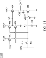
- Fig. 15 is a block diagram of a latch unit in accordance with another embodiment of the disclosure.
- the gate terminal of the sixth transistor M6 is controlled by the second latch signal SL2
- the gate terminal of the first transistor M1 is controlled by the first latch signal SL1.
- the first latch signal SL1 is configured to drive the first LED unit XLED1
- the second latch signal SL2 is configured to drive the second LED unit XLED2, in which the second LED unit XLED2 is illuminated prior to the first LED unit XLED1.
- the latch unit 1500 further includes a seventh transistor M7. As shown in Fig. 15 , the seventh transistor M7 provides the supply voltage VDD to the first node N1 according to the second latch signal SL2. Since the second LED unit XLED2 is illuminated prior to the first LED unit XLED1, the second latch signal SL2 is also prior to the first latch signal SL1.
- the second latch signal SL2 turns ON the sixth transistor M6 and the seventh transistor M7 so that the first node N1 is coupled to the supply voltage VDD and the second node N2 is coupled to the ground.
- the effect of the first preset transistor MR1 and the second preset transistor MR2 in Fig. 9 and that of the first preset transistor MR1 and the third transistor MR3 in Fig. 10 can be achieved by the seventh transistor M7.
- the latch unit comprises a plurality of transistors implemented by P-type transistors.
- the plurality of transistors may be implemented by N-type transistors as well.
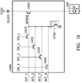
- Fig. 16 is a block diagram of the PWM circuit in Fig. 3 in accordance with an embodiment of the disclosure.
- the PWM circuit 1600 comprises a plurality of transistors implemented by N-type transistors.
- the PWM circuit 1600 includes a first transmission transistor 1610, a second transmission transistor 1620, a third transmission transistor 1630, a fourth transmission transistor 1640, a pull-down transistor 1650, and a dimming transistor 1660.
- the first transmission transistor 1610, the second transmission transistor 1620, the third transmission transistor 1630, the fourth transmission transistor 1640, and the dimming transistor 1660 correspond to the first transmission transistor 410, the second transmission transistor 420, the third transmission transistor 430, the fourth transmission transistor 440, and the dimming transistor 460 respectively, except for being N-type transistors.
- the pull-down transistor 1750 is configured to pull the PWM signal SPWM down to the ground level. According to the embodiment shown in Fig. 16 , the gate terminal of the pull-down transistor 1750 is controlled by the PWM signal SPWM. In other words, the pull-down transistor 1750 is gate-to-drain connected.
- the pull-down transistor 1750 may be controlled by other signals, such as the latch signal SL.
- the PWM circuit 1600 includes a first pull-down transistor and a second pull-down transistor (not shown in Fig. 16 ) which are controlled by the first latch signal SL1 and the second latch signal SL2 respectively.
- the pull-down transistor 1750 can be replaced by a pull-up transistor.
- the pull-up transistor 1750 is configured to pull the PWM signal SPWM up to the supply voltage VDD.
- Fig. 17 is a block diagram of a latch unit in accordance with another embodiment of the disclosure, in which the latch unit comprises a plurality of transistors implemented by N-type transistors. Comparing the latch unit 1700 to the latch unit 800 in Fig. 8 , all the P-type transistors in the latch unit 800 are converted into N-type transistors with some required modifications to be the latch unit 1700.
- the bootstrap transistor MBST in Fig. 17 is coupled between the first node N1 and the gate terminal of the second transistor M2, and the gate terminal of the bootstrap transistor MBST is coupled to the supply voltage VDD.
- the bootstrap capacitor CBST in Fig. 17 is coupled between the gate terminal of the second transistor M2 and the control bit CBIT.
- Fig. 18 is a block diagram of a latch unit in accordance with another embodiment of the disclosure, in which the latch unit comprises a plurality of transistors implemented by N-type transistors. Comparing the latch unit 1800 to the latch unit 911, all the P-type transistors in the latch unit 911 are converted into N-type transistors to be the latch unit 1800. Comparing the latch unit 1800 to the latch unit 1700, the latch unit 1800 further includes the first preset transistor MR1 and the second preset transistor MR2.
- the first preset transistor MR1 couples the first node N1 to the ground according to the second latch signal SL2.
- the second preset transistor MR2 provides the supply voltage VDD to the second node N2 according to the second latch signal SL2. Therefore, the voltages of both terminals of the bootstrap capacitor CBST can be preset to the ground.
- Fig. 19 is a block diagram of an LED driving array in accordance with another embodiment of the disclosure.
- the LED driving array 1900 includes a first LED driving circuit 1910 and a second LED driving circuit 1920.
- the LED driving array 1900 may include a plurality of LED driving circuits.
- the LED driving array 1900 including two LED driving circuits are illustrated herein, but not intended to be limited thereto.
- the first LED driving circuit 1910 is configured to illuminate the first LED unit XLED1 according to the data signal SD and the first latch signal SL1
- the second LED driving circuit 1920 is configured to illuminate the second LED unit XLED2 according to the data signal SD and the second latch signal SL2.
- the second LED unit XLED2 is illuminated prior to the first LED unit XLED1.
- the first LED driving circuit 1910 includes a plurality of latch units 1911, each of which generates a corresponding bit of the control signal SC (i.e., the control bit CBIT) to the PWM circuit 1912.
- the PWM circuit 1912 corresponds to the PWM circuit 1600 in Fig. 16 , which is not repeated herein.
- the second preset transistor MR2 of the latch unit 1800 in Fig. 18 is replaced by a third preset transistor MR3 in the latch unit 1911 in Fig. 19 .
- the third preset transistor MR3 couples the control bit CBIT to the ground in response to the second latch signal SL2, in which the second latch signal SL2 is configured to illuminate the second LED unit XLED2 which is illuminated prior to the first LED unit XLED1.
- the control bit CBIT and the voltage of the gate terminal of the second transistor M2 are preset to the supply voltage VDD, the voltages of both terminals of the bootstrap capacitor CBST are preset to the ground.
- the positive data DP at the high voltage level which is the supply voltage VDD
- the second transistor M2 is turned ON so that the voltage of the control bit CBIT is pulled up from the ground.
- the voltage rise of the control bit CBIT the voltage rise is coupled to the gate terminal of the second transistor M2 through the bootstrap capacitor CBST so that the gate terminal of the second transistor M2 is further pulled up to a voltage exceeding zero to completely turn ON the second transistor M2.
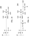
- Fig. 20 is a block diagram of a latch unit in accordance with another embodiment of the disclosure. Comparing the latch unit 2000 to the latch unit 1700 in Fig. 17 , the latch unit 2000 includes the bootstrap capacitor CBST, and the first transistor M1, the first capacitor C1, the second transistor M2, the bootstrap transistor MBST, and the third transistor M3, the second capacitor C2, the fourth transistor M4 are omitted.
- Fig. 21 is a block diagram of a latch unit in accordance with another embodiment of the disclosure. Comparing the latch unit 2100 to the latch unit 1911, the third preset transistor MR3, and the first transistor M1, the first capacitor C1, and the second transistor M2 of the latch unit 1911 are omitted. Comparing the latch unit 2100 to the latch unit 1200, all the P-type transistors of the latch unit 1200 have been converted into N-type transistors with some required modifications to be the latch unit 2100.
- Fig. 22 is a block diagram of a latch unit in accordance with another embodiment of the disclosure. Comparing the latch unit 2200 to the latch unit 1300 in Fig. 13 , all the P-type transistors of the latch unit 1300 have been converted into N-type transistors with some required modifications to be the latch unit 2200.
- the fifth transistor M5 and the sixth transistor M6 are configured to act as an inverter to invert the positive data DP sampled by the first transistor M1.
- the gate terminal of the fifth transistor M5 is supplied by the supply voltage. According to other embodiments of the disclosure, the gate terminal of the fifth transistor M5 could be controlled by other signals.
- Fig. 23 is a block diagram of a latch unit in accordance with another embodiment of the disclosure. Comparing the latch unit 2300 to the latch unit 2200 in Fig. 22 , the latch unit 2300 further includes the bootstrap capacitor CBST and the bootstrap transistor MBST.
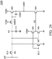
- Fig. 24 is a block diagram of a latch unit in accordance with another embodiment of the disclosure. Comparing the latch unit 2400 to the latch unit 1500 in Fig. 15 , all the P-type transistors of the latch unit 1500 have been converted into N-type transistors with some required modifications.
- the gate terminal of the fifth transistor M5 is controlled by the second latch signal SL2, and the gate terminal of the third transistor M1 is controlled by the first latch signal SL1.
- the first latch signal SL1 is configured to drive the first LED unit XLED1
- the second latch signal SL2 is configured to drive the second LED unit XLED2, in which the second LED unit XLED2 is illuminated prior to the first LED unit XLED1.
- the fifth transistor M5 is configured to preset the first node N1 to the supply voltage VDD according to the second latch signal SL2
- the seventh transistor M7 is configured to preset the second node N2 to the ground according to the second latch signal SL2.
Landscapes
- Engineering & Computer Science (AREA)
- Physics & Mathematics (AREA)
- Computer Hardware Design (AREA)
- General Physics & Mathematics (AREA)
- Theoretical Computer Science (AREA)
- Control Of Indicators Other Than Cathode Ray Tubes (AREA)
- Control Of El Displays (AREA)
Abstract
Description
- The disclosure relates generally to circuits for driving LED units, and more particularly it relates to circuits for dimming with pulse-width modulation (PWM).
- Active matrix LED display/backlight with mini- and micro-LED and OLED, equips a current driver to control the luminance of LED units in each pixel. The driver is serially connected to the LED between two voltage sources in order to control the current of the LED for luminance adjustment.
- It is not stable for an LED unit to operate with a low current, and the chromaticity of an LED unit is current-dependent. Therefore, PWM (Pulse Width Modulation) with fixed optimum LED current, instead of current controlling, has been proposed as a solution to the issues stated above.
- On the other hand, for some technical benefits, such as the stability that is characteristic of a TFT device, a lower-temperature process (the organic material of a flexible substrate may not be destroyed by the temperature), cost, etc., either PMOSs or NMOSs, instead of CMOSs, process can be utilized. Therefore, an LED driving circuit comprising either P-type transistors or N-type transistors is required.
- In an embodiment, an LED driving circuit for illuminating a first LED unit is provided. The LED driving circuit comprises: a data latch circuit, a current source, and a PWM circuit. The data latch circuit latches a data signal according to a first latch signal to generate a first control signal. The current source generates a constant current. The PWM circuit periodically passes the constant current through the first LED unit according to the first control signal and an enable signal.
- A detailed description is given in the following embodiments with reference to the accompanying drawings.
- The disclosure can be more fully understood by reading the subsequent detailed description and examples with references made to the accompanying drawings, wherein:
-
Fig. 1 is a block diagram of an LED driving circuit in accordance with an embodiment of the disclosure; -
Fig. 2 is a block diagram of an LED driving circuit in accordance with an embodiment of the disclosure; -
Fig. 3 is a block diagram of an LED driving circuit in accordance with an embodiment of the disclosure; -
Fig. 4 is a block diagram of thePWM circuit 230 inFig. 2 in accordance with an embodiment of the disclosure; -
Fig. 5 is a block diagram of a latch unit in accordance with an embodiment of the disclosure; -
Fig. 6 is a block diagram of a latch unit in accordance with another embodiment of the disclosure; -
Fig. 7 is a block diagram of a latch unit in accordance with another embodiment of the disclosure; -
Fig. 8 is a block diagram of a latch unit in accordance with another embodiment of the disclosure; -
Fig. 9 is a block diagram of an LED driving array in accordance with another embodiment of the disclosure; -
Fig. 10 is a block diagram of an LED driving array in accordance with another embodiment of the disclosure; -
Fig. 11 is a block diagram of a latch unit in accordance with another embodiment of the disclosure; -
Fig. 12 is a block diagram of a latch unit in accordance with another embodiment of the disclosure; -
Fig. 13 is a block diagram of a latch unit in accordance with another embodiment of the disclosure; -
Fig. 14 is a block diagram of a latch unit in accordance with another embodiment of the disclosure; -
Fig. 15 is a block diagram of a latch unit in accordance with another embodiment of the disclosure; -
Fig. 16 is a block diagram of the PWM circuit inFig. 3 in accordance with an embodiment of the disclosure; -
Fig. 17 is a block diagram of a latch unit in accordance with another embodiment of the disclosure; and -
Fig. 18 is a block diagram of an LED driving array in accordance with another embodiment of the disclosure. -
Fig. 19 is a block diagram of an LED driving array in accordance with another embodiment of the disclosure. -
Fig. 20 is a block diagram of a latch unit in accordance with another embodiment of the disclosure. -
Fig. 21 is a block diagram of a latch unit in accordance with another embodiment of the disclosure. -
Fig. 22 is a block diagram of a latch unit in accordance with another embodiment of the disclosure. -
Fig. 23 is a block diagram of a latch unit in accordance with another embodiment of the disclosure. -
Fig. 24 is a block diagram of a latch unit in accordance with another embodiment of the disclosure. - This description is made for the purpose of illustrating the general principles of the disclosure and should not be taken in a limiting sense. In addition, the present disclosure may repeat reference numerals and/or letters in the various examples. This repetition is for the purpose of simplicity and clarity and does not in itself dictate a relationship between the various embodiments and/or configurations discussed. The scope of the disclosure is best determined by reference to the appended claims.
- It is understood that the following disclosure provides many different embodiments, or examples, for implementing different features of the application. Specific examples of components and arrangements are described below to simplify the present disclosure. These are, of course, merely examples and are not intended to be limiting. In addition, the present disclosure may repeat reference numerals and/or letters in the various examples. This repetition is for the purpose of simplicity and clarity and does not in itself dictate a relationship between the various embodiments and/or configurations discussed. Moreover, the formation of a feature on, connected to, and/or coupled to another feature in the present disclosure that follows may include embodiments in which the features are formed in direct contact, and may also include embodiments in which additional features may be formed interposing the features, such that the features may not be in direct contact.
-
Fig. 1 is a block diagram of an LED driving circuit in accordance with an embodiment of the disclosure. As shown inFig. 1 , theLED driving circuit 100 is configured to illuminate the LED unit XLED, which includes adata latch circuit 110, a current source 120, and aPWM circuit 130. - According to an embodiment of the disclosure, the
LED driving circuit 100 may comprise a plurality of transistors implemented by P-type transistors. According to another embodiment of the disclosure, theLED driving circuit 100 may comprise a plurality of transistors implemented by N-type transistors. In other words, theLED driving circuit 100 may comprise a plurality of transistors implemented by either P-type transistors or N-type transistors. - The
data latch circuit 110 latches the data signal SD according to a latch signal SL to generate the control signal SC. The current source 120 generates a constant current IC. ThePWM circuit 130 periodically passes the constant current IC according to the control signal SC and the enable signal EN so that the constant current IC flows through the LED unit XLED. As shown inFig. 1 , whether the current source 120 sinks or sources the constant current IC is based on whether theLED driving circuit 100 is implemented by P-type transistors or N-type transistors. -
Fig. 2 is a block diagram of an LED driving circuit in accordance with an embodiment of the disclosure, in which the LED driving circuit inFig. 2 comprises a plurality of transistors implemented by P-type transistors. As shown inFig. 2 , theLED driving circuit 200 includes a data latch circuit 210, acurrent source 220, and aPWM circuit 230, in which the data latch circuit 210, thecurrent source 220, and thePWM circuit 230 correspond to thedata latch circuit 110, the current source 120, and thePWM circuit 130 inFig. 1 . TheLED driving circuit 200 couples the constant current IC to the LED unit XLED so that the constant current IC flows through the LED unit XLED to the ground. -
Fig. 3 is a block diagram of an LED driving circuit in accordance with another embodiment of the disclosure, in which the LED driving circuit inFig. 3 comprises a plurality of transistors implemented by N-type transistors. As shown inFig. 3 , theLED driving circuit 300 includes adata latch circuit 310, acurrent source 320, and aPWM circuit 330, in which thedata latch circuit 310, thecurrent source 320, and thePWM circuit 330 correspond to thedata latch circuit 110, the current source 120, and thePWM circuit 130 inFig. 1 . TheLED driving circuit 300 couples the constant current IC to the LED unit XLED so that the constant current IC flows through the LED unit XLED from the supply voltage VDD. - According to an embodiment of the disclosure, the data signal SD, the control signal SC, and the enable signal EN are N bits, in which N is a positive integer. Thus, the data latch circuit 210 in
Fig. 2 , or thedata latch circuit 310 inFig. 3 , comprises N latch units. Each of the latch units latches a corresponding bit of the data signal SD to generate a corresponding bit of the control signal SC. - Since N-type transistors and P-type transistors are complementary, one skilled in the art will understand how to modify the embodiments of the LED driving circuit with P-type transistors provided as follows to obtain the LED driving circuit with N-type transistors. In the following paragraphs, the LED driving circuit with P-type transistors are illustrated, but not intended to be limited to the embodiments with P-type transistors.
-
Fig. 4 is a block diagram of thePWM circuit 230 inFig. 2 in accordance with an embodiment of the disclosure. As shown inFig. 4 , thePWM circuit 400 includes afirst transmission transistor 410, asecond transmission transistor 420, athird transmission transistor 430, afourth transmission transistor 440, a pull-uptransistor 450, and a dimmingtransistor 460. - According to an embodiment of the disclosure, the data signal SD, the control signal SC, and the enable signal EN are illustrated as 4-bit herein, but not intended to be limited thereto. The control signal SC includes a first bit BIT_1, a second bit BIT_2, a third bit BIT_3, and a fourth bit BIT_4, and the enable signal EN includes a first enable EN_1, a second enable EN_2, a third enable EN_3, and a fourth enable EN_4.
- As shown in
Fig. 4 , thefirst transmission transistor 410, thesecond transmission transistor 420, thethird transmission transistor 430, and thefourth transmission transistor 440 respectively pass the first bit BIT_1, the second bit BIT_2, the third bit BIT_3, and the fourth bit BIT_4 to a PWM signal SPWM according to the first enable EN_1, the second enable EN_2, the third enable EN_3, and the fourth enable EN_4. According to the embodiment shown inFig. 4 , the duty cycles of the first enable EN_1, the second enable EN_2, the third enable EN_3, and the fourth enable EN_4 are 50%, 25%, 12.5%, and 6.25% respectively. - The dimming
transistor 460 is turned ON according to the PWM signal SPWM so that the constant current IC can flow through the LED unit XLED to illuminate the LED unit XLED. According to an embodiment of the disclosure, the pull-uptransistor 450 pulls the PWM signal SPWM up to the supply voltage VDD to turn OFF the dimmingtransistor 460 when thefirst transmission transistor 410, thesecond transmission transistor 420, thethird transmission transistor 430, and thefourth transmission transistor 440 are all turned OFF. - According to an embodiment of the disclosure, the LED unit XLED in
Fig. 4 is normally OFF, and the first bit BIT_1, the second bit BIT_2, the third bit BIT_3, and the fourth bit BIT_4 are configured to turn ON the LED unit XLED. According to an embodiment of the disclosure, as illustrated inFig. 4 , the gate terminal of the pull-uptransistor 450 is controlled by the PWM signal SPWM. Namely, the gate terminal of the pull-uptransistor 450 is coupled to its drain terminal. According to other embodiments of the disclosure, the gate terminal of the pull-uptransistor 450 may be controlled by another signal, such as the latch signal SL. - According to another embodiment of the disclosure, the
PWM circuit 400 may include a first pull-up transistor and a second pull-up transistor (not shown inFig. 4 ) which are controlled by a first latch signal SL1 and a second latch signal SL2, in which the first latch signal SL1 is configured to drive the LED unit XLED inFig. 4 , and the second latch signal SL2 is configured to drive another LED unit (not shown inFig. 4 ). The first latch signal SL1 and the second latch signal SL2 will be described in the following paragraphs. - According to an embodiment of the disclosure, the
first transmission transistor 410, thesecond transmission transistor 420, thethird transmission transistor 430, or thefourth transmission transistor 440 is turned ON by the first enable EN_1, the second enable EN_2, the third enable EN_3, or the fourth enable EN_4 at the low voltage level. In other words, thefirst transmission transistor 410, thesecond transmission transistor 420, thethird transmission transistor 430, and thefourth transmission transistor 440 are active low. -
Fig. 5 is a block diagram of a latch unit in accordance with an embodiment of the disclosure. Referring toFig. 1 , thedata latch circuit 110 includes a plurality of latch units. According to an embodiment of the disclosure, the latch unit of thedata latch circuit 110 is thelatch unit 500 inFig. 5 . As shown inFig. 5 , thelatch unit 500 generates a control bit CBIT which corresponds to any one of the first bit BIT_1, the second bit BIT_2, the third bit BIT_3, and the fourth bit BIT_4 of the control signal SC inFig. 4 according to a corresponding data bit DB of the data signal SD. - As shown in
Fig. 5 , thelatch unit 500 includes a first transistor M1, a first capacitor C1, a second transistor M2, a third transistor M3, a second capacitor C2, and a fourth transistor M4. According to an embodiment of the disclosure, the data signal SD includes a plurality of data bits DB, in which each data bit DB includes positive data DP and negative data DN, in which the negative data DN is an inverse of the positive data DP. - The first transistor M1 provides the negative data DN from a data bit DB of the data signal SD to a first node N1 according to the latch signal SL. The first capacitor C1, which is coupled between the first node N1 and the ground, stores the negative data DN. The second transistor M2 couples a control bit CBIT of the control signal SC to the ground according to the negative data DN stored in the first capacitor C1. According to an embodiment of the disclosure, the control bit CBIT in
Fig. 5 may be any one of the first bit BIT_1, the second bit BIT_2, the third bit BIT_3, and thefourth bit BIT 4 of the control signal SC inFig. 4 . - According to an embodiment of the disclosure, the negative data DN ranges from a low voltage level to a high voltage level, in which the low voltage level should be less than the ground by the absolute value of the threshold voltage of the second transistor M2 so that the second transistor M2 can be completely turned ON when the negative data DN is at the low voltage level.
- As shown in
Fig. 5 , the third transistor M3 provides the positive data DP from the data bit DB of the data signal SD to a second node N2 according to the latch signal SL. The second capacitor C2, which is coupled between the second node N2 and the ground, stores the positive data DP. The fourth transistor M4 provides the supply voltage VDD to the control bit CBIT of the control signal SC according to the positive data DP at the second node N2. - According to an embodiment of the disclosure, in order to implement the
latch unit 500 with P-type transistors, the first capacitor C1 and the second capacitor C2 are required to form a pair of memory units, and the second transistor M2 and the fourth transistor M4 form a complementary push-pull driver to generate the control bit CBIT of the control signal SD. -
Fig. 6 is a block diagram of a latch unit in accordance with another embodiment of the disclosure. As shown inFig. 6 , thelatch unit 600 includes the first transistor M1, the first capacitor C1, the second transistor M2 ofFig. 5 . According to an embodiment of the disclosure, a plurality of thelatch units 600 are coupled to a corresponding one of the first bit BIT_1, the second bit BIT_2, the third bit BIT_3, and the fourth bit BIT_4 of thePWM circuit 60, and only onelatch unit 600 is illustrated herein. - According to an embodiment of the disclosure, the
PWM circuit 60 includes afirst transmission transistor 61, asecond transmission transistor 62, athird transmission transistor 63, afourth transmission transistor 64, a pull-uptransistor 65, and a dimmingtransistor 66, which corresponds to thePWM circuit 400. - According to an embodiment of the disclosure, since the second transistor M2 is configured to pull the control bit CBIT down to the ground to turn ON the dimming
transistor 66, the pull-uptransistor 65 is required to normally turn OFF the dimmingtransistor 66 when thefirst transmission transistor 61, thesecond transmission transistor 62, thethird transmission transistor 63, and thefourth transmission transistor 64 are all OFF. According to an embodiment of the disclosure, the low voltage level of the negative data DN should be less than the ground level by an absolute value of the threshold voltage of the second transistor M2. -
Fig. 7 is a block diagram of a latch unit in accordance with another embodiment of the disclosure. As shown inFig. 7 , thelatch unit 700 includes the third transistor M3, the second capacitor C2, and the fourth transistor M4. As shown inFig. 7 , a plurality of thelatch units 700 are coupled to a corresponding one of the first bit BIT_1, the second bit BIT_2, the third bit BIT_3, and the fourth bit BIT_4 of thePWM circuit 70, and only onelatch unit 700 is illustrated herein. - The
PWM circuit 70 includes afirst transmission transistor 71, asecond transmission transistor 72, a third transmission transistor 73, a fourth transmission transistor 74, a pull-down transistor 75, and a dimmingtransistor 76, which corresponds to thePWM circuit 400 inFig. 4 . - According to an embodiment of the disclosure, since the fourth transistor M4 in
Fig. 7 is configured to pull the control bit CBIT up to the supply voltage VDD, the pull-down transistor 75 is required to normally turn ON the dimmingtransistor 76 when thefirst transmission transistor 71, thesecond transmission transistor 72, the third transmission transistor 73, and the fourth transmission transistor 74 are all OFF. According to an embodiment of the disclosure, the first enable EN_1, the second enable EN_2, the third enable EN_3, and the fourth enable EN_4 inFig. 7 are allowed to overlap since each of the first bit BIT_1, the second bit BIT_2, the third bit BIT_3, and the fourth bit BIT_4 is high impedance in the high logic level. - As shown in
Fig. 7 , the pull-down transistor 75 pulls the PWM signal SPWM down to the ground. According to an embodiment of the disclosure, as illustrated inFig. 7 , the gate terminal of the pull-down transistor 75 is tied to the ground. According to other embodiments of the disclosure, the gate terminal of the pull-down transistor 75 may be controlled by another signal, such as the latch signal SL. - According to an embodiment of the disclosure, since the fourth transistor M4 of the
latch unit 700 is configured to pull the control bit CBIT up to the supply voltage VDD, the pull-down transistor 75 is configured to normally pull the PWM signal SPWM down to the ground level when thefirst transmission transistor 71, thesecond transmission transistor 72, the third transmission transistor 73, and the fourth transmission transistor 74 are all OFF. - According to an embodiment of the disclosure, it is allowable that the first enable EN_1, the second enable EN_2, the third enable EN_3, and the fourth enable EN_4 are overlapped since the control bit CBIT is in a high impedance state when the control bit CBIT is at the high voltage level.
-
Fig. 8 is a block diagram of a latch unit in accordance with another embodiment of the disclosure. Comparing thelatch unit 800 inFig. 8 to thelatch unit 500 inFig. 5 , thelatch unit 800 further includes a bootstrap transistor MBST and a bootstrap capacitor CBST. - As shown in
Fig. 8 , the bootstrap transistor MBST is coupled between the first node N1 and the gate terminal of the second transistor M2, and the gate terminal of the bootstrap transistor MBST is coupled to the ground. The bootstrap capacitor CBST is coupled between the control bit CBIT and the gate terminal of the second transistor M2. According to an embodiment of the disclosure, the low voltage level of the negative data DN can be as low as the ground level of thelatch unit 800. - According to an embodiment of the disclosure, the bootstrap transistor MBST and the bootstrap capacitor CBST are configured to completely turn ON the second transistor M2 so that the control bit CBIT can be pulled down to the ground. However, the effect of the bootstrap transistor MBST and the bootstrap capacitor CBST could be limited if the voltage difference between two terminals of the bootstrap capacitance CBST is small when the control bit CBIT is at the low voltage level before the latch signal SL turns ON the first transistor M1.
-
Fig. 9 is a block diagram of an LED driving array in accordance with another embodiment of the disclosure. As shown inFig. 9 , theLED driving array 900 includes a firstLED driving circuit 910 and a secondLED driving circuit 920. According to other embodiments of the disclosure, theLED driving array 900 may include a plurality of LED driving circuits. TheLED driving array 900 including two LED driving circuits are illustrated herein, but not intended to be limited thereto. - The first
LED driving circuit 910 is configured to illuminate the first LED unit XLED1 according to the data signal SD and the first latch signal SL1, and the secondLED driving circuit 920 is configured to illuminate the second LED unit XLED2 according to the data signal SD and the second latch signal SL2. - According to an embodiment of the disclosure, the second LED unit XLED2 is illuminated prior to the first LED unit XLED1. In other words, the second latch signal SL2 is activated prior to the first latch signal SL1. According to an embodiment of the disclosure, the second LED unit XLED2 is placed near the first LED unit XLED1 and illuminated prior to the first LED unit XLED1. Thus, the second latch signal SL2 may be viewed as a latch signal prior to the first latch signal SL1.
- As shown in
Fig. 9 , the firstLED driving circuit 910 includes a plurality oflatch units 911, each of which generates a corresponding bit of the control signal SC (i.e., the control bit CBIT) to thePWM circuit 912. According to an embodiment of the disclosure, thePWM circuit 912 corresponds to thePWM circuit 400 inFig. 4 , which is not repeated herein. - As shown in
Fig. 9 , the PWM circuit includes a pull-up transistor PU. According to an embodiment of the disclosure, the pull-up transistor PU is controlled by the PWM signal SPWM. Namely, the gate terminal of the pull-up transistor PU is coupled to its drain terminal. According to another embodiment of the disclosure, the gate terminal of the pull-up transistor PU is controlled by the first latch signal SL1. According to another embodiment of the disclosure, the gate terminal of the pull-up transistor PU is controlled by the second latch signal SL2. - Comparing the
latch unit 911 inFig. 9 to thelatch unit 800 inFig. 8 , thelatch unit 911 further includes a first preset transistor MR1 and a second preset transistor MR2. The first preset transistor MR1 is configured to provide the supply voltage VDD to the first node N1 according to the second latch signal SL2. The second present transistor MR2 is configured to provide the ground to the second node N2 according to the second latch signal SL2. - According to an embodiment of the disclosure, the second LED unit XLED2 is turned ON prior to the first LED unit XLED1. When the second LED unit XLED2 is turned ON according to the second latch signal SL2, the second latch signal SL2 is also configured to turn ON the first preset transistor MR1 and the second preset transistor MR2 of the
latch unit 911 in the firstLED driving circuit 910 to preset the voltages of the control bit CBIT and the first node N1. - According to an embodiment of the disclosure, when the first preset transistor MR1 and the second preset transistor MR2 are turned ON, the voltage of the first node N1 is pulled up to the supply voltage VDD, and the voltage of the second node N2 is pull down to the ground level. Thus, the second transistor M2 is turned OFF and the fourth transistor M4 is turned ON so that the control bit CBIT is pulled up to the supply voltage VDD. In other words, the voltages of both terminals of the bootstrap capacitor CBST are preset to the supply voltage VDD by the second latch signal SL2.
- According to an embodiment of the disclosure, when the bootstrap capacitor CBST is preset and the negative data DN at the low voltage level, which is the ground level, is sampled by the first latch signal SL1, the voltage of the gate terminal of the second transistor M2 is equal to an absolute value of the threshold voltage of the bootstrap transistor MBST since the bootstrap transistor MBST is turned OFF.
- Since the voltage of the control bit CBIT is pulled down from the supply voltage VDD, the voltage of the gate terminal of the second transistor M2 can be further pulled down due to the voltage drop on the control bit CBIT coupled by the bootstrap capacitor CBST. Therefore, the voltage of the gate terminal of the second transistor M2 can be lower than zero volts to completely turn ON the second transistor M2. In addition, the bootstrap transistor MBST is configured to separate the first node N1 and the gate terminal of the second transistor M2 so that the gate terminal of the second transistor M2 can be better pulled down to a voltage lower than zero by AC coupling through the bootstrap capacitor CBST.
- As shown in
Fig. 9 , the PWM circuit includes a pull-up transistor PU. According to an embodiment of the disclosure, the pull-up transistor PU is controlled by the PWM signal SPWM. Namely, the gate terminal of the pull-up transistor PU is coupled to its drain terminal. According to another embodiment of the disclosure, the gate terminal of the pull-up transistor PU is controlled by the first latch signal SL1 (not shown inFig. 9 ). According to another embodiment of the disclosure, the gate terminal of the pull-up transistor PU is controlled by the second latch signal SL2 (not shown inFig. 9 ). -
Fig. 10 is a block diagram of an LED driving array in accordance with another embodiment of the disclosure. As shown inFig. 10 , theLED driving array 1000 includes a firstLED driving circuit 1010 and a secondLED driving circuit 1020. According to other embodiments of the disclosure, theLED driving array 1000 may include a plurality of LED driving circuits. TheLED driving array 1000 including two LED driving circuits are illustrated herein, but not intended to be limited thereto. - The first
LED driving circuit 1010 is configured to illuminate the first LED unit XLED1 according to the data signal SD and the first latch signal SL1, and the secondLED driving circuit 1020 is configured to illuminate the second LED unit XLED2 according to the data signal SD and the second latch signal SL2. According to an embodiment of the disclosure, the second LED unit XLED2 is illuminated prior to the first LED unit XLED1. - Comparing the first
LED driving circuit 1010 to the firstLED driving circuit 910 inFig. 9 , the second preset transistor MR2 of thelatch unit 911 inFig. 9 is replaced by a third preset transistor MR3 in thelatch unit 1011 inFig. 10 and thePWM circuit 1020 corresponds to thePWM circuit 400 inFig. 4 . - The third preset transistor MR3 provides the supply voltage VDD to the control bit CBIT in response to the second latch signal SL2, in which the second latch signal SL2 is configured to illuminate the second LED unit XLED2 which is illuminated prior to the first LED unit XLED1.
- Since the control bit CBIT and the voltage of the gate terminal of the second transistor M2 are preset to the supply voltage VDD, the voltages of both terminals of the bootstrap capacitor CBST are preset to the supply voltage VDD. When the negative data DN at the low voltage level, which is the ground level, is sampled to the first node N1 by the first latch signal SL1, the second transistor M2 is turned ON so that the voltage of the control bit CBIT is pulled down from the supply voltage VDD. During the voltage drop of the control bit CBIT, the voltage drop is coupled to the gate terminal of the second transistor M2 through the bootstrap capacitor CBST so that the gate terminal of the second transistor M2 is further pulled down to a voltage lower than zero to completely turn ON the second transistor M2.
-
Fig. 11 is a block diagram of a latch unit in accordance with another embodiment of the disclosure. Comparing thelatch unit 1100 to thelatch unit 800 inFig. 8 , thelatch unit 1100 includes the first transistor M1, the first capacitor C1, the second transistor M2, the bootstrap transistor MBST, and the bootstrap capacitor CBST, and the third transistor M3, the second capacitor C2, and the fourth transistor M4 are omitted. - According to an embodiment of the disclosure, the low voltage level of the negative data DN can be as low as the ground level of the
latch unit 1100. According to an embodiment of the disclosure, since the third transistor M3, the second capacitor C2, and the fourth transistor M4 of thelatch unit 800 are omitted, the area of thelatch unit 1100 can be reduced so that the cost can be reduced as well. - According to an embodiment of the disclosure, the low voltage level of the negative data DN can be as low as the ground with the aid of the bootstrap capacitor CBST and the bootstrap transistor MBST.
-
Fig. 12 is a block diagram of a latch unit in accordance with another embodiment of the disclosure. Comparing thelatch unit 1200 to thelatch unit 1011 inFig. 10 , thelatch unit 1200 includes the first transistor M1, the first capacitor C1, the second transistor M2, the bootstrap transistor MBST, the bootstrap capacitor CBST, the first preset transistor MR1, and the third preset transistor MR3, and the third transistor M3, the second capacitor C2, and the fourth transistor M4 are omitted. - According to an embodiment of the disclosure, the low voltage level of the negative data DN can be as low as the ground level of the
latch unit 1200. According to an embodiment of the disclosure, since the third transistor M3, the second capacitor C2, and the fourth transistor M4 of thelatch unit 1011 are omitted, the area of thelatch unit 1200 can be reduced so that the cost can be reduced as well. -
Fig. 13 is a block diagram of a latch unit in accordance with another embodiment of the disclosure. Comparing thelatch unit 1300 to thelatch unit 500 inFig. 5 , the third transistor M3 and the second capacitor C2 are replaced by a fifth transistor M5 and a sixth transistor M6. - According to an embodiment of the disclosure, the fifth transistor M5 and the sixth transistor M6 are configured to act as an inverter to invert the negative data DN. Thus, the positive data DP and the second capacitor C2 shown in
Figs. 5 ,8 , and9 are no longer required. According to an embodiment of the disclosure, the gate terminal of the sixth transistor M6 is coupled to the ground. According to other embodiments of the disclosure, the gate terminal of the sixth transistor M6 could be controlled by other signals. - According to an embodiment of the disclosure, by incorporating the fifth transistor M5 and the sixth transistor M6, the positive data DP can be reduced so that the I/O interface of the data signal SD can be reduced as well. According to an embodiment of the disclosure, the low voltage level of the negative data DN should be less than the ground level by an absolute value of the threshold voltage of the second transistor M2 to completely turn ON the second transistor M2.
-
Fig. 14 is a block diagram of a latch unit in accordance with another embodiment of the disclosure. Comparing thelatch unit 1400 to thelatch unit 1300 inFig. 13 , thelatch unit 1400 further includes the bootstrap capacitor CBST and the bootstrap transistor MBST. - According to an embodiment of the disclosure, the low voltage level of the negative data DN in
Fig. 14 could be equal to the ground level due to the bootstrap capacitor CBST and the bootstrap transistor MBST. The effect of the bootstrap capacitor CBST and the bootstrap transistor MBST is stated above, which is not repeated herein. -
Fig. 15 is a block diagram of a latch unit in accordance with another embodiment of the disclosure. As shown inFig. 15 , the gate terminal of the sixth transistor M6 is controlled by the second latch signal SL2, and the gate terminal of the first transistor M1 is controlled by the first latch signal SL1. As stated inFigs. 9-10 , the first latch signal SL1 is configured to drive the first LED unit XLED1, and the second latch signal SL2 is configured to drive the second LED unit XLED2, in which the second LED unit XLED2 is illuminated prior to the first LED unit XLED1. - Comparing the
latch unit 1500 to thelatch unit 1400 inFig. 14 , thelatch unit 1500 further includes a seventh transistor M7. As shown inFig. 15 , the seventh transistor M7 provides the supply voltage VDD to the first node N1 according to the second latch signal SL2. Since the second LED unit XLED2 is illuminated prior to the first LED unit XLED1, the second latch signal SL2 is also prior to the first latch signal SL1. - Thus, before the first latch signal SL1 activates the first transistor M1, the second latch signal SL2 turns ON the sixth transistor M6 and the seventh transistor M7 so that the first node N1 is coupled to the supply voltage VDD and the second node N2 is coupled to the ground. In other words, the effect of the first preset transistor MR1 and the second preset transistor MR2 in
Fig. 9 and that of the first preset transistor MR1 and the third transistor MR3 inFig. 10 can be achieved by the seventh transistor M7. - As shown in
Figs. 5-15 , the latch unit comprises a plurality of transistors implemented by P-type transistors. However, the plurality of transistors may be implemented by N-type transistors as well. -
Fig. 16 is a block diagram of the PWM circuit inFig. 3 in accordance with an embodiment of the disclosure. According to an embodiment of the disclosure, thePWM circuit 1600 comprises a plurality of transistors implemented by N-type transistors. As shown inFig. 16 , thePWM circuit 1600 includes afirst transmission transistor 1610, asecond transmission transistor 1620, athird transmission transistor 1630, afourth transmission transistor 1640, a pull-down transistor 1650, and adimming transistor 1660. - The
first transmission transistor 1610, thesecond transmission transistor 1620, thethird transmission transistor 1630, thefourth transmission transistor 1640, and thedimming transistor 1660 correspond to thefirst transmission transistor 410, thesecond transmission transistor 420, thethird transmission transistor 430, thefourth transmission transistor 440, and the dimmingtransistor 460 respectively, except for being N-type transistors. - The pull-
down transistor 1750 is configured to pull the PWM signal SPWM down to the ground level. According to the embodiment shown inFig. 16 , the gate terminal of the pull-down transistor 1750 is controlled by the PWM signal SPWM. In other words, the pull-down transistor 1750 is gate-to-drain connected. - According to other embodiments of the disclosure, the pull-
down transistor 1750 may be controlled by other signals, such as the latch signal SL. According to another embodiment of the disclosure, thePWM circuit 1600 includes a first pull-down transistor and a second pull-down transistor (not shown inFig. 16 ) which are controlled by the first latch signal SL1 and the second latch signal SL2 respectively. - According to other embodiments of the disclosure, the pull-
down transistor 1750 can be replaced by a pull-up transistor. The pull-uptransistor 1750 is configured to pull the PWM signal SPWM up to the supply voltage VDD. -
Fig. 17 is a block diagram of a latch unit in accordance with another embodiment of the disclosure, in which the latch unit comprises a plurality of transistors implemented by N-type transistors. Comparing thelatch unit 1700 to thelatch unit 800 inFig. 8 , all the P-type transistors in thelatch unit 800 are converted into N-type transistors with some required modifications to be thelatch unit 1700. - The bootstrap transistor MBST in
Fig. 17 is coupled between the first node N1 and the gate terminal of the second transistor M2, and the gate terminal of the bootstrap transistor MBST is coupled to the supply voltage VDD. The bootstrap capacitor CBST inFig. 17 is coupled between the gate terminal of the second transistor M2 and the control bit CBIT. -
Fig. 18 is a block diagram of a latch unit in accordance with another embodiment of the disclosure, in which the latch unit comprises a plurality of transistors implemented by N-type transistors. Comparing thelatch unit 1800 to thelatch unit 911, all the P-type transistors in thelatch unit 911 are converted into N-type transistors to be thelatch unit 1800. Comparing thelatch unit 1800 to thelatch unit 1700, thelatch unit 1800 further includes the first preset transistor MR1 and the second preset transistor MR2. - As shown in
Fig. 18 , the first preset transistor MR1 couples the first node N1 to the ground according to the second latch signal SL2. The second preset transistor MR2 provides the supply voltage VDD to the second node N2 according to the second latch signal SL2. Therefore, the voltages of both terminals of the bootstrap capacitor CBST can be preset to the ground. -
Fig. 19 is a block diagram of an LED driving array in accordance with another embodiment of the disclosure. As shown inFig. 19 , theLED driving array 1900 includes a firstLED driving circuit 1910 and a second LED driving circuit 1920. According to other embodiments of the disclosure, theLED driving array 1900 may include a plurality of LED driving circuits. TheLED driving array 1900 including two LED driving circuits are illustrated herein, but not intended to be limited thereto. - The first
LED driving circuit 1910 is configured to illuminate the first LED unit XLED1 according to the data signal SD and the first latch signal SL1, and the second LED driving circuit 1920 is configured to illuminate the second LED unit XLED2 according to the data signal SD and the second latch signal SL2. According to an embodiment of the disclosure, the second LED unit XLED2 is illuminated prior to the first LED unit XLED1. - The first
LED driving circuit 1910 includes a plurality oflatch units 1911, each of which generates a corresponding bit of the control signal SC (i.e., the control bit CBIT) to thePWM circuit 1912. According to an embodiment of the disclosure, thePWM circuit 1912 corresponds to thePWM circuit 1600 inFig. 16 , which is not repeated herein. - Comparing the
latch unit 1911 to thelatch unit 1800 inFig. 18 , the second preset transistor MR2 of thelatch unit 1800 inFig. 18 is replaced by a third preset transistor MR3 in thelatch unit 1911 inFig. 19 . The third preset transistor MR3 couples the control bit CBIT to the ground in response to the second latch signal SL2, in which the second latch signal SL2 is configured to illuminate the second LED unit XLED2 which is illuminated prior to the first LED unit XLED1. - Since the control bit CBIT and the voltage of the gate terminal of the second transistor M2 are preset to the supply voltage VDD, the voltages of both terminals of the bootstrap capacitor CBST are preset to the ground. When the positive data DP at the high voltage level, which is the supply voltage VDD, is sampled to the first node N1 by the first latch signal SL1, the second transistor M2 is turned ON so that the voltage of the control bit CBIT is pulled up from the ground. During the voltage rise of the control bit CBIT, the voltage rise is coupled to the gate terminal of the second transistor M2 through the bootstrap capacitor CBST so that the gate terminal of the second transistor M2 is further pulled up to a voltage exceeding zero to completely turn ON the second transistor M2.
-
Fig. 20 is a block diagram of a latch unit in accordance with another embodiment of the disclosure. Comparing thelatch unit 2000 to thelatch unit 1700 inFig. 17 , thelatch unit 2000 includes the bootstrap capacitor CBST, and the first transistor M1, the first capacitor C1, the second transistor M2, the bootstrap transistor MBST, and the third transistor M3, the second capacitor C2, the fourth transistor M4 are omitted. - Comparing the
latch unit 2000 to thelatch unit 1100 inFig. 11 , all the P-type transistors have been converted into N-type transistors with some required modifications to be thelatch unit 2000. -
Fig. 21 is a block diagram of a latch unit in accordance with another embodiment of the disclosure. Comparing thelatch unit 2100 to thelatch unit 1911, the third preset transistor MR3, and the first transistor M1, the first capacitor C1, and the second transistor M2 of thelatch unit 1911 are omitted. Comparing thelatch unit 2100 to thelatch unit 1200, all the P-type transistors of thelatch unit 1200 have been converted into N-type transistors with some required modifications to be thelatch unit 2100. -
Fig. 22 is a block diagram of a latch unit in accordance with another embodiment of the disclosure. Comparing thelatch unit 2200 to thelatch unit 1300 inFig. 13 , all the P-type transistors of thelatch unit 1300 have been converted into N-type transistors with some required modifications to be thelatch unit 2200. - As shown in
Fig. 22 , the fifth transistor M5 and the sixth transistor M6 are configured to act as an inverter to invert the positive data DP sampled by the first transistor M1. The gate terminal of the fifth transistor M5 is supplied by the supply voltage. According to other embodiments of the disclosure, the gate terminal of the fifth transistor M5 could be controlled by other signals. -
Fig. 23 is a block diagram of a latch unit in accordance with another embodiment of the disclosure. Comparing thelatch unit 2300 to thelatch unit 2200 inFig. 22 , thelatch unit 2300 further includes the bootstrap capacitor CBST and the bootstrap transistor MBST. - Comparing the
latch unit 2300 to thelatch unit 1400 inFig. 14 , all the P-type transistors of thelatch unit 1400 has been converted into N-type transistors with some required modifications. -
Fig. 24 is a block diagram of a latch unit in accordance with another embodiment of the disclosure. Comparing thelatch unit 2400 to thelatch unit 1500 inFig. 15 , all the P-type transistors of thelatch unit 1500 have been converted into N-type transistors with some required modifications. - As shown in
Fig. 24 , the gate terminal of the fifth transistor M5 is controlled by the second latch signal SL2, and the gate terminal of the third transistor M1 is controlled by the first latch signal SL1. As stated inFig. 19 , the first latch signal SL1 is configured to drive the first LED unit XLED1, and the second latch signal SL2 is configured to drive the second LED unit XLED2, in which the second LED unit XLED2 is illuminated prior to the first LED unit XLED1. - Therefore, the fifth transistor M5 is configured to preset the first node N1 to the supply voltage VDD according to the second latch signal SL2, and the seventh transistor M7 is configured to preset the second node N2 to the ground according to the second latch signal SL2.
- While the disclosure has been described by way of example and in terms of preferred embodiment, it should be understood that the disclosure is not limited thereto. Those who are skilled in this technology can still make various alterations and modifications without departing from the scope and spirit of this disclosure. Therefore, the scope of the present disclosure shall be defined and protected by the following claims and their equivalents.
Claims (15)
- An LED driving circuit (100; 200; 300) for illuminating a first LED unit (XLED, comprising:a data latch circuit (110; 210; 310, latching a data signal according to a first latch signal (SL) to generate a first control signal (SC);a current source (120; 220; 320, generating a constant current; anda PWM circuit (130; 230; 400), comprising:a plurality of transmission transistors (410, 420, ..., 440), wherein each of the transmission transistors passes a corresponding bit of the first control signal (SC) to generate a PWM signal (SPWM) according to a corresponding bit of an enable signal (EN_1 ... EN_4); anda dimming transistor (460), coupling the current source to the first LED unit according to the PWM signal so that the constant current flows through the first LED unit;wherein the plurality of transmission transistors, the pull-up transistor, and the dimming transistor are implemented by either P-type transistors or N-type transistors.
- The LED driving circuit of claim 1, wherein the PWM circuit further comprises:
a pull-up transistor (450), pulling the PWM signal to a supply voltage when all the transmission transistors are turned OFF. - The LED driving circuit of claim 2, wherein each of the latch units (500) comprises:a first transistor (M1), providing negative data from a first data bit of the data signal to a first node according to a first latch bit of the first latch signal;a first capacitor (C1), coupled between the first node and a ground and storing the negative data; anda second transistor (M2), coupling a first bit of the first control signal to the ground according to the negative data at the first node.
- The LED driving circuit of claim 3, wherein each of the latch units (800) further comprises:a bootstrap transistor (MBST), coupled between the first node and a gate terminal of the second transistor, wherein a gate terminal of the bootstrap transistor is coupled to the ground; anda bootstrap capacitor (CBST), coupled between the first bit of the first control signal and the gate terminal of the second transistor.
- The LED driving circuit of claim 4, wherein each of the latch units (911) further comprises:a first preset transistor (MR1), providing the supply voltage to the first node (N1) according to a second latch signal; anda third preset transistor (MR3), providing the supply voltage to the first bit of the first control signal according to the second latch signal, wherein the second latch signal is configured to illuminate a second LED unit, wherein the second LED unit is turned ON prior to the first LED unit.
- The LED driving circuit of claim 4, wherein each of the latch units further comprises:a third transistor (M3), providing positive data from the first data bit of the data signal to a second node according to the first latch bit of the first latch signal, wherein the positive data is an inverse of the negative data;a second capacitor (C2), coupled between the second node and the ground and storing the positive data; anda fourth transistor (M4), providing the supply voltage to the first bit of the first control signal according to the positive data at the second node.
- The LED driving circuit of claim 6, wherein each of the latch units further comprises:a first preset transistor (MR1), providing the supply voltage to the first node according to a second latch signal; anda second preset transistor (MR2), providing the ground to the second node (N2) according to the second latch signal, wherein the second latch signal is configured to illuminate a second LED unit, wherein the second LED unit is turned ON prior to the first LED unit.
- The LED driving circuit of claim 3, wherein each of the latch units further comprises:a fourth transistor (M4), providing the supply voltage to the first bit of the first control signal according to a voltage of a second node;a fifth transistor (M5), providing the supply voltage to the second node according to the negative data at the first node; anda sixth transistor (M6), coupling the second node to the ground.
- The LED driving circuit of claim 1, wherein the PWM circuit further comprises:
a pull-down transistor (1750), pulling the PWM signal (SPWM) to a ground when all the transmission transistors are turned OFF. - The LED driving circuit of claim 9, wherein each of the latch units comprises:a first transistor (M1), providing positive data from a first data bit of the data signal to a first node according to a first latch bit of the first latch signal;a first capacitor (C1), coupled between the first node and a ground and storing the positive data; anda second transistor (M2), coupling a supply voltage to a first bit of the first control signal according to the positive data at the first node.
- The LED driving circuit of claim 10, wherein each of the latch units further comprises:a bootstrap transistor (MBST), coupled between the first node and a gate terminal of the second transistor, wherein a gate terminal of the bootstrap transistor is coupled to the supply voltage; anda bootstrap capacitor (CBST), coupled between the first bit of the first control signal and the gate terminal of the second transistor.
- The LED driving circuit of claim 11, wherein each of the latch units further comprises:a first preset transistor (MR1), coupling the first node to the ground according to a second latch signal; anda third preset transistor (M3), coupling the first bit of the first control signal to the ground according to the second latch signal, wherein the second latch signal is configured to illuminate a second LED unit, wherein the second LED unit is turned ON prior to the first LED unit.
- The LED driving circuit of claim 11, wherein each of the latch units further comprises:a third transistor (M3), providing negative data from the first data bit of the data signal to a second node according to the first latch bit of the first latch signal, wherein the negative data is an inverse of the positive data;a second capacitor (C2), coupled between the second node and the ground and storing the negative data; anda fourth transistor (M4), coupling the first bit of the first control signal to the ground according to the negative data at the second node.
- The LED driving circuit of claim 13, wherein each of the latch units further comprises:a first preset transistor (MR1), coupling the first node to the ground according to a second latch signal; anda second preset transistor (MR2), providing the supply voltage to the second node according to the second latch signal, wherein the second latch signal is configured to illuminate a second LED unit, wherein the second LED unit is turned ON prior to the first LED unit.
- The LED driving circuit of claim 10, wherein each of the latch units comprises:a fourth transistor (M4), coupling the first bit of the first control signal to the ground according to a voltage of a second node;a fifth transistor (M5), providing the supply voltage to the second node according to the positive data at the first node; anda sixth transistor (M6), coupling the second node to the ground.
Applications Claiming Priority (2)
| Application Number | Priority Date | Filing Date | Title |
|---|---|---|---|
| US201862716908P | 2018-08-09 | 2018-08-09 | |
| US16/255,208 US10455653B1 (en) | 2018-08-09 | 2019-01-23 | LED driving circuits |
Publications (2)
| Publication Number | Publication Date |
|---|---|
| EP3608900A1 true EP3608900A1 (en) | 2020-02-12 |
| EP3608900B1 EP3608900B1 (en) | 2022-06-29 |
Family
ID=68242030
Family Applications (1)
| Application Number | Title | Priority Date | Filing Date |
|---|---|---|---|
| EP19186837.1A Active EP3608900B1 (en) | 2018-08-09 | 2019-07-17 | Led driving circuits |
Country Status (4)
| Country | Link |
|---|---|
| US (1) | US10455653B1 (en) |
| EP (1) | EP3608900B1 (en) |
| KR (1) | KR102569144B1 (en) |
| CN (1) | CN110859016B (en) |
Cited By (1)
| Publication number | Priority date | Publication date | Assignee | Title |
|---|---|---|---|---|
| EP4152614A1 (en) * | 2021-09-16 | 2023-03-22 | InnoLux Corporation | Electronic device |
Families Citing this family (12)
| Publication number | Priority date | Publication date | Assignee | Title |
|---|---|---|---|---|
| WO2019046633A1 (en) * | 2017-08-30 | 2019-03-07 | Planar Systems, Inc. | Current controller for output stage of led driver circuitry |
| US10885830B2 (en) * | 2018-07-24 | 2021-01-05 | Innolux Corporation | Electronic device capable of reducing color shift |
| TWI747119B (en) * | 2018-12-27 | 2021-11-21 | 聯詠科技股份有限公司 | Circuit and method for driving light sources |
| CN109473058B (en) * | 2019-01-23 | 2022-04-15 | 京东方科技集团股份有限公司 | Display device, display control device and method |
| CN110111727A (en) * | 2019-06-03 | 2019-08-09 | 京东方科技集团股份有限公司 | A kind of pixel-driving circuit and its driving method, display device |
| CN116324956A (en) * | 2020-10-01 | 2023-06-23 | 株式会社半导体能源研究所 | Display device and electronic device |
| CN114930445B (en) * | 2020-12-03 | 2026-01-02 | 三星电子株式会社 | Display device and its light-emitting device |
| KR102361974B1 (en) * | 2020-12-03 | 2022-02-14 | 삼성전자주식회사 | Display apparatus and light apparatus thereof |
| US11723131B2 (en) * | 2021-04-09 | 2023-08-08 | Innolux Corporation | Display device |
| TWI802215B (en) * | 2022-01-11 | 2023-05-11 | 友達光電股份有限公司 | Driving circuit |
| CN115394255B (en) * | 2022-08-30 | 2025-05-16 | 合肥视涯显示科技有限公司 | Silicon-based display panel and display device |
| KR102769779B1 (en) | 2023-10-25 | 2025-02-17 | 엘지전자 주식회사 | Image display apparatus, and video wall including the same |
Citations (4)
| Publication number | Priority date | Publication date | Assignee | Title |
|---|---|---|---|---|
| US20090108768A1 (en) * | 2007-10-30 | 2009-04-30 | Chih-Hsiang Yang | Backlight control device and method for controlling a driving current of an led |
| US20090134814A1 (en) * | 2007-11-26 | 2009-05-28 | Seung Hwan Moon | Backlight unit, display device comprising the same, and control method thereof |
| US20180110100A1 (en) * | 2016-10-17 | 2018-04-19 | Integrated Silicon Solution, Inc. | Power supply transient reduction method for multiple led channel systems |
| EP3557569A1 (en) * | 2018-04-19 | 2019-10-23 | InnoLux Corporation | Led pixel circuits with pwm dimming |
Family Cites Families (14)
| Publication number | Priority date | Publication date | Assignee | Title |
|---|---|---|---|---|
| KR100318277B1 (en) * | 1999-08-17 | 2002-01-18 | 이종하 | Apparatus For Controlling Color Level of Image Display System with Light Emitting Diode Array and method for controlling the same |
| JP3681121B2 (en) * | 2001-06-15 | 2005-08-10 | キヤノン株式会社 | Driving circuit and display device |
| US6501230B1 (en) * | 2001-08-27 | 2002-12-31 | Eastman Kodak Company | Display with aging correction circuit |
| CN1983365B (en) * | 2002-04-26 | 2011-05-18 | 东芝松下显示技术有限公司 | Drive circuit for electroluminescence display screen |
| JP5124985B2 (en) * | 2006-05-23 | 2013-01-23 | ソニー株式会社 | Image display device |
| JP4655111B2 (en) * | 2008-05-20 | 2011-03-23 | 日本テキサス・インスツルメンツ株式会社 | LED device and LED drive circuit |
| US20110199011A1 (en) * | 2009-01-09 | 2011-08-18 | Ken Nakazawa | Light-emitting diode driving circuit and planar illuminating device having same |
| KR101974218B1 (en) * | 2012-05-04 | 2019-05-02 | 매그나칩 반도체 유한회사 | Led driver apparatus |
| US9548021B2 (en) * | 2012-06-01 | 2017-01-17 | Samsung Display Co., Ltd. | Method of driving light-source and display apparatus for performing the method |
| TWI548112B (en) * | 2013-05-14 | 2016-09-01 | 友達光電股份有限公司 | Light emitting diode module |
| US9420647B2 (en) * | 2014-02-25 | 2016-08-16 | Earl W. McCune, Jr. | Dimming and voltage protection method and apparatus for solid-state lighting |
| KR20180002786A (en) * | 2015-06-05 | 2018-01-08 | 애플 인크. | Emission control devices and methods for display panel |
| JP6594690B2 (en) * | 2015-07-22 | 2019-10-23 | ローム株式会社 | Current driver, LED drive circuit, lighting device, electronic equipment |
| US10206252B2 (en) * | 2016-09-08 | 2019-02-12 | Infineon Technologies Ag | Driving several light sources |
-
2019
- 2019-01-23 US US16/255,208 patent/US10455653B1/en active Active
- 2019-04-30 KR KR1020190050788A patent/KR102569144B1/en active Active
- 2019-07-17 EP EP19186837.1A patent/EP3608900B1/en active Active
- 2019-07-18 CN CN201910650595.8A patent/CN110859016B/en active Active
Patent Citations (4)
| Publication number | Priority date | Publication date | Assignee | Title |
|---|---|---|---|---|
| US20090108768A1 (en) * | 2007-10-30 | 2009-04-30 | Chih-Hsiang Yang | Backlight control device and method for controlling a driving current of an led |
| US20090134814A1 (en) * | 2007-11-26 | 2009-05-28 | Seung Hwan Moon | Backlight unit, display device comprising the same, and control method thereof |
| US20180110100A1 (en) * | 2016-10-17 | 2018-04-19 | Integrated Silicon Solution, Inc. | Power supply transient reduction method for multiple led channel systems |
| EP3557569A1 (en) * | 2018-04-19 | 2019-10-23 | InnoLux Corporation | Led pixel circuits with pwm dimming |
Non-Patent Citations (2)
| Title |
|---|
| ANONYMOUS: "Decoders and Multiplexers", 11 March 2015 (2015-03-11), XP055568540, Retrieved from the Internet <URL:https://web.archive.org/web/20150311084120/http://www.dcs.gla.ac.uk/~simon/teaching/CS1Q-students/systems/online/sec7.html> [retrieved on 20190313] * |
| KAYED S I ET AL: "A new efficient design of the 2-to-1 multiplexer", MICROELECTRONICS, 1995. PROCEEDINGS., 1995 20TH INTERNATIONAL CONFEREN CE ON NIS, SERBIA 12-14 SEPT. 1995, NEW YORK, NY, USA,IEEE, US, vol. 2, 12 September 1995 (1995-09-12), pages 817 - 822, XP010161787, ISBN: 978-0-7803-2786-3, DOI: 10.1109/ICMEL.1995.500974 * |
Cited By (1)
| Publication number | Priority date | Publication date | Assignee | Title |
|---|---|---|---|---|
| EP4152614A1 (en) * | 2021-09-16 | 2023-03-22 | InnoLux Corporation | Electronic device |
Also Published As
| Publication number | Publication date |
|---|---|
| EP3608900B1 (en) | 2022-06-29 |
| CN110859016A (en) | 2020-03-03 |
| US10455653B1 (en) | 2019-10-22 |
| KR102569144B1 (en) | 2023-08-21 |
| CN110859016B (en) | 2021-05-07 |
| KR20200018215A (en) | 2020-02-19 |
Similar Documents
| Publication | Publication Date | Title |
|---|---|---|
| US10455653B1 (en) | LED driving circuits | |
| TWI716160B (en) | Pixel circuit | |
| KR101937064B1 (en) | Low-temperature polycrystalline silicon semiconductor thin-film transistor-based goa circuit | |
| US8847661B2 (en) | Level shift device | |
| CN110085161B (en) | Display panel and pixel circuit | |
| TWI699742B (en) | Pixel circuit | |
| TWI827311B (en) | Pixel circuit and display panel | |
| CN114078430A (en) | Pixel circuit and display panel | |
| KR101943234B1 (en) | Low-temperature polycrystalline silicon semiconductor thin-film transistor-based goa circuit | |
| CN104812144A (en) | High performance adaptive switched led driver | |
| US11462151B2 (en) | Light emitting device | |
| CN113302843B (en) | Level Shifter for Half-Bridge GaN Driver Applications | |
| CN116434701B (en) | Pixel circuit, driving method and display panel | |
| US9978333B2 (en) | Timing sequences generation circuits and liquid crystal devices | |
| CN104867448A (en) | Active organic light emitting diode circuit and driving method thereof | |
| US8416006B1 (en) | Electronic device with gate driver for high voltage level shifter | |
| US20230099245A1 (en) | Light emitting element drive device and light emitting system | |
| CN114203103B (en) | Light-emitting circuit, backlight module and display panel | |
| US11018655B2 (en) | Level shift circuit and display driver integrated circuit | |
| TWI653616B (en) | Pixel circuit | |
| CN112270909B (en) | Pixel driving circuit | |
| CN112509516A (en) | Display device | |
| KR101943233B1 (en) | Low-temperature polycrystalline silicon semiconductor thin-film transistor-based goa circuit | |
| CN114708828A (en) | Pixel circuit and display panel | |
| CN101399525A (en) | Voltage level clamping circuit and comparator module |
Legal Events
| Date | Code | Title | Description |
|---|---|---|---|
| PUAI | Public reference made under article 153(3) epc to a published international application that has entered the european phase |
Free format text: ORIGINAL CODE: 0009012 |
|
| STAA | Information on the status of an ep patent application or granted ep patent |
Free format text: STATUS: THE APPLICATION HAS BEEN PUBLISHED |
|
| AK | Designated contracting states |
Kind code of ref document: A1 Designated state(s): AL AT BE BG CH CY CZ DE DK EE ES FI FR GB GR HR HU IE IS IT LI LT LU LV MC MK MT NL NO PL PT RO RS SE SI SK SM TR |
|
| AX | Request for extension of the european patent |
Extension state: BA ME |
|
| STAA | Information on the status of an ep patent application or granted ep patent |
Free format text: STATUS: REQUEST FOR EXAMINATION WAS MADE |
|
| 17P | Request for examination filed |
Effective date: 20200728 |
|
| RBV | Designated contracting states (corrected) |
Designated state(s): AL AT BE BG CH CY CZ DE DK EE ES FI FR GB GR HR HU IE IS IT LI LT LU LV MC MK MT NL NO PL PT RO RS SE SI SK SM TR |
|
| STAA | Information on the status of an ep patent application or granted ep patent |
Free format text: STATUS: EXAMINATION IS IN PROGRESS |
|
| 17Q | First examination report despatched |
Effective date: 20210407 |
|
| REG | Reference to a national code |
Ref country code: DE Ref legal event code: R079 Ref document number: 602019016348 Country of ref document: DE Free format text: PREVIOUS MAIN CLASS: G09G0003340000 Ipc: G09G0003320000 |
|
| GRAP | Despatch of communication of intention to grant a patent |
Free format text: ORIGINAL CODE: EPIDOSNIGR1 |
|
| STAA | Information on the status of an ep patent application or granted ep patent |
Free format text: STATUS: GRANT OF PATENT IS INTENDED |
|
| RIC1 | Information provided on ipc code assigned before grant |
Ipc: G09G 3/34 20060101ALI20220112BHEP Ipc: H05B 45/39 20200101ALI20220112BHEP Ipc: H05B 45/10 20200101ALI20220112BHEP Ipc: G09G 3/32 20160101AFI20220112BHEP |
|
| INTG | Intention to grant announced |
Effective date: 20220201 |
|
| GRAS | Grant fee paid |
Free format text: ORIGINAL CODE: EPIDOSNIGR3 |
|
| GRAA | (expected) grant |
Free format text: ORIGINAL CODE: 0009210 |
|
| STAA | Information on the status of an ep patent application or granted ep patent |
Free format text: STATUS: THE PATENT HAS BEEN GRANTED |
|
| AK | Designated contracting states |
Kind code of ref document: B1 Designated state(s): AL AT BE BG CH CY CZ DE DK EE ES FI FR GB GR HR HU IE IS IT LI LT LU LV MC MK MT NL NO PL PT RO RS SE SI SK SM TR |
|
| REG | Reference to a national code |
Ref country code: CH Ref legal event code: EP |
|
| REG | Reference to a national code |
Ref country code: DE Ref legal event code: R096 Ref document number: 602019016348 Country of ref document: DE |
|
| REG | Reference to a national code |
Ref country code: AT Ref legal event code: REF Ref document number: 1501853 Country of ref document: AT Kind code of ref document: T Effective date: 20220715 |
|
| REG | Reference to a national code |
Ref country code: IE Ref legal event code: FG4D |
|
| REG | Reference to a national code |
Ref country code: LT Ref legal event code: MG9D |
|
| PG25 | Lapsed in a contracting state [announced via postgrant information from national office to epo] |
Ref country code: SE Free format text: LAPSE BECAUSE OF FAILURE TO SUBMIT A TRANSLATION OF THE DESCRIPTION OR TO PAY THE FEE WITHIN THE PRESCRIBED TIME-LIMIT Effective date: 20220629 Ref country code: NO Free format text: LAPSE BECAUSE OF FAILURE TO SUBMIT A TRANSLATION OF THE DESCRIPTION OR TO PAY THE FEE WITHIN THE PRESCRIBED TIME-LIMIT Effective date: 20220929 Ref country code: LT Free format text: LAPSE BECAUSE OF FAILURE TO SUBMIT A TRANSLATION OF THE DESCRIPTION OR TO PAY THE FEE WITHIN THE PRESCRIBED TIME-LIMIT Effective date: 20220629 Ref country code: HR Free format text: LAPSE BECAUSE OF FAILURE TO SUBMIT A TRANSLATION OF THE DESCRIPTION OR TO PAY THE FEE WITHIN THE PRESCRIBED TIME-LIMIT Effective date: 20220629 Ref country code: GR Free format text: LAPSE BECAUSE OF FAILURE TO SUBMIT A TRANSLATION OF THE DESCRIPTION OR TO PAY THE FEE WITHIN THE PRESCRIBED TIME-LIMIT Effective date: 20220930 Ref country code: FI Free format text: LAPSE BECAUSE OF FAILURE TO SUBMIT A TRANSLATION OF THE DESCRIPTION OR TO PAY THE FEE WITHIN THE PRESCRIBED TIME-LIMIT Effective date: 20220629 Ref country code: BG Free format text: LAPSE BECAUSE OF FAILURE TO SUBMIT A TRANSLATION OF THE DESCRIPTION OR TO PAY THE FEE WITHIN THE PRESCRIBED TIME-LIMIT Effective date: 20220929 |
|
| REG | Reference to a national code |
Ref country code: NL Ref legal event code: MP Effective date: 20220629 |
|
| REG | Reference to a national code |
Ref country code: AT Ref legal event code: MK05 Ref document number: 1501853 Country of ref document: AT Kind code of ref document: T Effective date: 20220629 |
|
| PG25 | Lapsed in a contracting state [announced via postgrant information from national office to epo] |
Ref country code: RS Free format text: LAPSE BECAUSE OF FAILURE TO SUBMIT A TRANSLATION OF THE DESCRIPTION OR TO PAY THE FEE WITHIN THE PRESCRIBED TIME-LIMIT Effective date: 20220629 Ref country code: LV Free format text: LAPSE BECAUSE OF FAILURE TO SUBMIT A TRANSLATION OF THE DESCRIPTION OR TO PAY THE FEE WITHIN THE PRESCRIBED TIME-LIMIT Effective date: 20220629 |
|
| PG25 | Lapsed in a contracting state [announced via postgrant information from national office to epo] |
Ref country code: NL Free format text: LAPSE BECAUSE OF FAILURE TO SUBMIT A TRANSLATION OF THE DESCRIPTION OR TO PAY THE FEE WITHIN THE PRESCRIBED TIME-LIMIT Effective date: 20220629 |
|
| PG25 | Lapsed in a contracting state [announced via postgrant information from national office to epo] |
Ref country code: SM Free format text: LAPSE BECAUSE OF FAILURE TO SUBMIT A TRANSLATION OF THE DESCRIPTION OR TO PAY THE FEE WITHIN THE PRESCRIBED TIME-LIMIT Effective date: 20220629 Ref country code: SK Free format text: LAPSE BECAUSE OF FAILURE TO SUBMIT A TRANSLATION OF THE DESCRIPTION OR TO PAY THE FEE WITHIN THE PRESCRIBED TIME-LIMIT Effective date: 20220629 Ref country code: RO Free format text: LAPSE BECAUSE OF FAILURE TO SUBMIT A TRANSLATION OF THE DESCRIPTION OR TO PAY THE FEE WITHIN THE PRESCRIBED TIME-LIMIT Effective date: 20220629 Ref country code: PT Free format text: LAPSE BECAUSE OF FAILURE TO SUBMIT A TRANSLATION OF THE DESCRIPTION OR TO PAY THE FEE WITHIN THE PRESCRIBED TIME-LIMIT Effective date: 20221031 Ref country code: ES Free format text: LAPSE BECAUSE OF FAILURE TO SUBMIT A TRANSLATION OF THE DESCRIPTION OR TO PAY THE FEE WITHIN THE PRESCRIBED TIME-LIMIT Effective date: 20220629 Ref country code: EE Free format text: LAPSE BECAUSE OF FAILURE TO SUBMIT A TRANSLATION OF THE DESCRIPTION OR TO PAY THE FEE WITHIN THE PRESCRIBED TIME-LIMIT Effective date: 20220629 Ref country code: AT Free format text: LAPSE BECAUSE OF FAILURE TO SUBMIT A TRANSLATION OF THE DESCRIPTION OR TO PAY THE FEE WITHIN THE PRESCRIBED TIME-LIMIT Effective date: 20220629 |
|
| PG25 | Lapsed in a contracting state [announced via postgrant information from national office to epo] |
Ref country code: PL Free format text: LAPSE BECAUSE OF FAILURE TO SUBMIT A TRANSLATION OF THE DESCRIPTION OR TO PAY THE FEE WITHIN THE PRESCRIBED TIME-LIMIT Effective date: 20220629 Ref country code: IS Free format text: LAPSE BECAUSE OF FAILURE TO SUBMIT A TRANSLATION OF THE DESCRIPTION OR TO PAY THE FEE WITHIN THE PRESCRIBED TIME-LIMIT Effective date: 20221029 |
|
| REG | Reference to a national code |
Ref country code: CH Ref legal event code: PL |
|
| REG | Reference to a national code |
Ref country code: BE Ref legal event code: MM Effective date: 20220731 |
|
| REG | Reference to a national code |
Ref country code: DE Ref legal event code: R097 Ref document number: 602019016348 Country of ref document: DE |
|
| PG25 | Lapsed in a contracting state [announced via postgrant information from national office to epo] |
Ref country code: MC Free format text: LAPSE BECAUSE OF FAILURE TO SUBMIT A TRANSLATION OF THE DESCRIPTION OR TO PAY THE FEE WITHIN THE PRESCRIBED TIME-LIMIT Effective date: 20220629 Ref country code: AL Free format text: LAPSE BECAUSE OF FAILURE TO SUBMIT A TRANSLATION OF THE DESCRIPTION OR TO PAY THE FEE WITHIN THE PRESCRIBED TIME-LIMIT Effective date: 20220629 |
|
| PG25 | Lapsed in a contracting state [announced via postgrant information from national office to epo] |
Ref country code: LU Free format text: LAPSE BECAUSE OF NON-PAYMENT OF DUE FEES Effective date: 20220717 Ref country code: LI Free format text: LAPSE BECAUSE OF NON-PAYMENT OF DUE FEES Effective date: 20220731 Ref country code: DK Free format text: LAPSE BECAUSE OF FAILURE TO SUBMIT A TRANSLATION OF THE DESCRIPTION OR TO PAY THE FEE WITHIN THE PRESCRIBED TIME-LIMIT Effective date: 20220629 Ref country code: CZ Free format text: LAPSE BECAUSE OF FAILURE TO SUBMIT A TRANSLATION OF THE DESCRIPTION OR TO PAY THE FEE WITHIN THE PRESCRIBED TIME-LIMIT Effective date: 20220629 Ref country code: CH Free format text: LAPSE BECAUSE OF NON-PAYMENT OF DUE FEES Effective date: 20220731 |
|
| PLBE | No opposition filed within time limit |
Free format text: ORIGINAL CODE: 0009261 |
|
| STAA | Information on the status of an ep patent application or granted ep patent |
Free format text: STATUS: NO OPPOSITION FILED WITHIN TIME LIMIT |
|
| PG25 | Lapsed in a contracting state [announced via postgrant information from national office to epo] |
Ref country code: BE Free format text: LAPSE BECAUSE OF NON-PAYMENT OF DUE FEES Effective date: 20220731 |
|
| 26N | No opposition filed |
Effective date: 20230330 |
|
| PG25 | Lapsed in a contracting state [announced via postgrant information from national office to epo] |
Ref country code: IE Free format text: LAPSE BECAUSE OF NON-PAYMENT OF DUE FEES Effective date: 20220717 |
|
| PG25 | Lapsed in a contracting state [announced via postgrant information from national office to epo] |
Ref country code: SI Free format text: LAPSE BECAUSE OF FAILURE TO SUBMIT A TRANSLATION OF THE DESCRIPTION OR TO PAY THE FEE WITHIN THE PRESCRIBED TIME-LIMIT Effective date: 20220629 |
|
| PG25 | Lapsed in a contracting state [announced via postgrant information from national office to epo] |
Ref country code: IT Free format text: LAPSE BECAUSE OF FAILURE TO SUBMIT A TRANSLATION OF THE DESCRIPTION OR TO PAY THE FEE WITHIN THE PRESCRIBED TIME-LIMIT Effective date: 20220629 |
|
| PG25 | Lapsed in a contracting state [announced via postgrant information from national office to epo] |
Ref country code: HU Free format text: LAPSE BECAUSE OF FAILURE TO SUBMIT A TRANSLATION OF THE DESCRIPTION OR TO PAY THE FEE WITHIN THE PRESCRIBED TIME-LIMIT; INVALID AB INITIO Effective date: 20190717 |
|
| PG25 | Lapsed in a contracting state [announced via postgrant information from national office to epo] |
Ref country code: MK Free format text: LAPSE BECAUSE OF FAILURE TO SUBMIT A TRANSLATION OF THE DESCRIPTION OR TO PAY THE FEE WITHIN THE PRESCRIBED TIME-LIMIT Effective date: 20220629 Ref country code: CY Free format text: LAPSE BECAUSE OF FAILURE TO SUBMIT A TRANSLATION OF THE DESCRIPTION OR TO PAY THE FEE WITHIN THE PRESCRIBED TIME-LIMIT Effective date: 20220629 |
|
| PG25 | Lapsed in a contracting state [announced via postgrant information from national office to epo] |
Ref country code: TR Free format text: LAPSE BECAUSE OF FAILURE TO SUBMIT A TRANSLATION OF THE DESCRIPTION OR TO PAY THE FEE WITHIN THE PRESCRIBED TIME-LIMIT Effective date: 20220629 |
|
| PG25 | Lapsed in a contracting state [announced via postgrant information from national office to epo] |
Ref country code: MT Free format text: LAPSE BECAUSE OF FAILURE TO SUBMIT A TRANSLATION OF THE DESCRIPTION OR TO PAY THE FEE WITHIN THE PRESCRIBED TIME-LIMIT Effective date: 20220629 |
|
| PG25 | Lapsed in a contracting state [announced via postgrant information from national office to epo] |
Ref country code: BG Free format text: LAPSE BECAUSE OF FAILURE TO SUBMIT A TRANSLATION OF THE DESCRIPTION OR TO PAY THE FEE WITHIN THE PRESCRIBED TIME-LIMIT Effective date: 20220629 |
|
| PG25 | Lapsed in a contracting state [announced via postgrant information from national office to epo] |
Ref country code: BG Free format text: LAPSE BECAUSE OF FAILURE TO SUBMIT A TRANSLATION OF THE DESCRIPTION OR TO PAY THE FEE WITHIN THE PRESCRIBED TIME-LIMIT Effective date: 20220629 |
|
| PGFP | Annual fee paid to national office [announced via postgrant information from national office to epo] |
Ref country code: GB Payment date: 20250626 Year of fee payment: 7 |
|
| PGFP | Annual fee paid to national office [announced via postgrant information from national office to epo] |
Ref country code: DE Payment date: 20250702 Year of fee payment: 7 |
|
| PGFP | Annual fee paid to national office [announced via postgrant information from national office to epo] |
Ref country code: FR Payment date: 20250703 Year of fee payment: 7 |