EP3607703B1 - Station d'abonné pour un système de bus et procédé d'amélioration du respect de l'exigence de rythme des bits dans un système de bus - Google Patents
Station d'abonné pour un système de bus et procédé d'amélioration du respect de l'exigence de rythme des bits dans un système de bus Download PDFInfo
- Publication number
- EP3607703B1 EP3607703B1 EP18716199.7A EP18716199A EP3607703B1 EP 3607703 B1 EP3607703 B1 EP 3607703B1 EP 18716199 A EP18716199 A EP 18716199A EP 3607703 B1 EP3607703 B1 EP 3607703B1
- Authority
- EP
- European Patent Office
- Prior art keywords
- transmission
- bus
- reception device
- control device
- signal
- Prior art date
- Legal status (The legal status is an assumption and is not a legal conclusion. Google has not performed a legal analysis and makes no representation as to the accuracy of the status listed.)
- Active
Links
- 238000000034 method Methods 0.000 title claims description 11
- 230000005540 biological transmission Effects 0.000 claims description 54
- 238000004891 communication Methods 0.000 claims description 48
- 239000003990 capacitor Substances 0.000 claims description 17
- 230000000630 rising effect Effects 0.000 claims description 7
- 230000003071 parasitic effect Effects 0.000 claims description 5
- 230000008859 change Effects 0.000 description 8
- 238000011156 evaluation Methods 0.000 description 6
- 238000012986 modification Methods 0.000 description 6
- 230000004048 modification Effects 0.000 description 6
- 238000010586 diagram Methods 0.000 description 4
- 238000005070 sampling Methods 0.000 description 3
- 230000008901 benefit Effects 0.000 description 2
- 230000003111 delayed effect Effects 0.000 description 2
- 238000012544 monitoring process Methods 0.000 description 2
- 238000007792 addition Methods 0.000 description 1
- 230000001419 dependent effect Effects 0.000 description 1
- 238000013461 design Methods 0.000 description 1
- 238000001514 detection method Methods 0.000 description 1
- 238000001914 filtration Methods 0.000 description 1
- 230000007257 malfunction Effects 0.000 description 1
- 238000013508 migration Methods 0.000 description 1
- 230000005012 migration Effects 0.000 description 1
- 230000008092 positive effect Effects 0.000 description 1
- 238000012545 processing Methods 0.000 description 1
- 230000001960 triggered effect Effects 0.000 description 1
Images

Classifications
-
- H—ELECTRICITY
- H04—ELECTRIC COMMUNICATION TECHNIQUE
- H04L—TRANSMISSION OF DIGITAL INFORMATION, e.g. TELEGRAPHIC COMMUNICATION
- H04L12/00—Data switching networks
- H04L12/28—Data switching networks characterised by path configuration, e.g. LAN [Local Area Networks] or WAN [Wide Area Networks]
- H04L12/40—Bus networks
- H04L12/40006—Architecture of a communication node
-
- H—ELECTRICITY
- H04—ELECTRIC COMMUNICATION TECHNIQUE
- H04L—TRANSMISSION OF DIGITAL INFORMATION, e.g. TELEGRAPHIC COMMUNICATION
- H04L12/00—Data switching networks
- H04L12/28—Data switching networks characterised by path configuration, e.g. LAN [Local Area Networks] or WAN [Wide Area Networks]
- H04L12/40—Bus networks
- H04L2012/40208—Bus networks characterized by the use of a particular bus standard
- H04L2012/40215—Controller Area Network CAN
Definitions
- the present invention relates to a subscriber station for a bus system and a method for improving compliance with the bit timing requirement in a bus system in order to achieve good reception quality even with a possible asymmetry of received bits at high data rates.
- a classic CAN frame is divided into an arbitration field and a data field.
- bit-by-bit arbitration is used to determine which of the participants in the bus system has exclusive access to a communication medium between the participants in the bus system.
- bit-by-bit arbitration is used to determine which of the participants in the bus system has exclusive access to a communication medium between the participants in the bus system.
- Bitrate_arb Bitrate_data.
- the maximum bit rate is 1 Mbps (mega bits per second), that means the bit time is 1 ⁇ s.
- CAN-FD The CAN protocol was further developed under the name CAN-FD, according to which messages are transmitted according to the specification "CAN with Flexible Data-Rate, Specification Version 1.0" (source http://www.semiconductors.bosch.de). With CAN-FD it is possible to increase the data rate for systems in which the data rate was previously limited by the bus length of the systems.
- bit rate_arb Bitrate_arb ⁇ Bitrate_data applies.
- the disclosure document DE 10 2014 204 050 A1 describes a subscriber station for a bus system one with a transmitting / receiving device for sending or receiving a message, the transmitting / receiving device having a device for processing the transmitted signal of a transmission signal to be transmitted by the transmitting / receiving device.
- This device is designed to set a predetermined bit symmetry of bits of the transmission signal by generating an internal transmission signal for the message, the dominant phase of the bits being shortened and the recessive phase of bits being lengthened in the internal transmission signal.
- the disclosure document DE 10 2014 223 838 A1 describes a subscriber station for a bus system with a detection unit for detecting a bit width of received bits of a message sent via a bus, and a control unit for determining the bit width of at least one bit of a message to be sent in order to meet the bus system requirements for the duty cycle and to regulate the bit width by delaying the edges of a transmission signal on the basis of the detected bit width.
- a subscriber station for a bus system and a method for improving compliance with the bit timing requirement in a bus system which solve the aforementioned problems.
- a subscriber station for a bus system and a method for improving compliance with the bit timing requirement in a bus system are to be provided in which compliance with the bit timing requirements can be met simply, effectively and inexpensively, so that no faulty transmissions appear.
- the object is achieved by a subscriber station for a bus system according to claim 1.
- Compliance with the bit timing requirement of the bus system is achieved through targeted wiring with at least one electrical resistor between the communication control device and the transceiver of an electronic control unit of the subscriber station.
- This makes it possible to migrate an electronic control unit (ECU) of the subscriber station from CAN to CAN-FD without having to exchange the transmitting / receiving device or the transceiver. Because of this, the migration from CAN to CAN-FD can take place without redevelopment of the transmitter / receiver device or the transceiver. This results in a clear cost advantage.
- ECU electronice control unit
- the configuration of the subscriber station described above can also be easily retrofitted to existing subscriber stations. This is particularly advantageous for subscriber stations that would have to be operated in the borderline area with regard to CAN FD bit timing. With the configuration of the subscriber station described above, a greater safety margin can be achieved for the required minimum bit time of an individual bit of the CAN frame. This gives the planner or designer of the bus system, such as a vehicle manufacturer or user, greater degrees of freedom when designing the bus topology and bit rate.
- the delay unit may have at least one resistor that forms an RC element with a capacitance that is connected between the communication control device and the transceiver, and a unit that is designed to provide a reception threshold for a received signal for a rising edge of the To delay the signal by a first predetermined value and to reduce it from a previous voltage level to a lower voltage level and to delay it by a second predetermined value for a falling edge of the signal and to reduce it from a previous voltage level to a lower voltage level.
- the capacitance can be a parasitic capacitance of the signal line between the communication control device and the transmitting / receiving device or also have the capacitance of a capacitor that is connected to the resistor as an RC element.
- the at least one resistor is connected between a connection of the communication control device, which is provided for a transmission signal to be transmitted by the communication control device, and a connection of the transmission / reception device, which is provided for the transmission signal transmitted by the communication control device.
- the capacitor can be connected at its one connection to the at least one resistor and the connection of the transmitting / receiving device for a transmission signal sent by the communication control device and connected to ground at its other connection.
- the at least one resistor is connected between a connection of the transmitting / receiving device, which is provided for a received signal received by the transmitting / receiving device from the bus, and a connection of the communication control device, which is intended for the transmission by the transmitting / receiving device.
- / Receiving device received from the bus is provided.
- the capacitor can be connected at its one connection to the at least one resistor and the connection (RxD) of the communication control device for a received signal received by the transmitting / receiving device and connected to ground at its other connection.
- the delay unit is designed to introduce the delay as a function of the bus state.
- the transmitting / receiving device can have a unit which is designed to delay the signal to be transmitted on the bus in time as a function of the bus state.
- the communication control device can have a unit which is designed to delay the transmission signal to be transmitted or the reception signal received from the bus by the transmission / reception device as a function of the bus status.
- the transmitting / receiving device can have a unit which is designed to reduce the bus level of a TxD driver and / or an RxD driver to belittle. In all of these design variants, compliance with the bit timing requirement of the bus system can be adapted very flexibly to the respective existing conditions.
- the subscriber station described above can be part of a bus system that has a bus and at least two subscriber stations which are connected to one another via the bus in such a way that they can communicate with one another, at least one of the at least two subscriber stations being a previously described subscriber station.
- the aforementioned object is also achieved by a method for improving compliance with the bit timing requirement in a bus system according to claim 10.
- the method offers the same advantages as mentioned above with regard to the subscriber station.
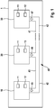
- Fig. 1 shows a bus system 1, which can be a CAN bus system, a CAN FD bus system, etc., for example.
- the bus system 1 can be used in a vehicle, in particular a motor vehicle, an airplane, etc., or in a hospital, etc. use.
- the bus system 1 has a plurality of subscriber stations 10, 20, 30, each of which is connected to a bus 40 with a first bus core 41 and a second bus core 42.
- the bus wires 41, 42 can also be called CAN_H and CAN_L and are used to couple the dominant levels in the transmission state.
- Messages 45, 46, 47 in the form of signals can be transmitted between the individual subscriber stations 10, 20, 30 via bus 40.
- the subscriber stations 10, 20, 30 can be, for example, control devices or display devices of a motor vehicle.
- the subscriber stations 10, 30 each have a communication control device 11 and a transmitting / receiving device 12.
- the subscriber station 20, on the other hand, has a communication control device 11 and a transmitting / receiving device 13.
- the transmitting / receiving devices 12 of the subscriber stations 10, 30 and the transmitter - / receiving device 13 of the subscriber stations 20 are each connected directly to the bus 40, even if this is shown in FIG Fig. 1 is not shown.
- the communication control device 11 is used to control communication between the respective subscriber station 10, 20, 30 via the bus 40 with another subscriber station of the subscriber stations 10, 20, 30 connected to the bus 40 CAN FD controller.
- the transmitting / receiving device 13 of the subscriber station 20 is used to send the messages 46 in the form of a transmit signal TX to another subscriber station of the bus system 1 and to receive the messages 45, 47 from the other subscriber stations of the bus system 1 in the form of a receive signal RX.
- the transmitting / receiving device 13 can be designed like a conventional CAN transceiver.
- Fig. 2 shows in its upper part based on the message 45 a CAN frame as it is sent by the transceiver 12 or the transceiver 13, and in its lower part a CAN FD frame, how it can be sent by the transmitting / receiving device 12.
- the messages 45, 47 are therefore possibly in each case a CAN frame or a CAN FD frame.
- the messages 46 may each be a CAN frame.
- the CAN frame and the CAN FD frame for the CAN communication on the bus 40 are basically divided into two different phases, namely the arbitration phases 451, 453 and a data area 452, which is also the data field for CAN-HS and for CAN -FD is also called data phase.
- the arbitration phases 451, 453 compared to the classic CAN, at the end of the arbitration phase 451 the bit rate for the following data phase is increased to, for example, 2, 4, 5, 8Mbps etc.
- the bit rate in the arbitration phases 451, 453 is lower than the bit rate in the data area 452.
- the data area 452 is significantly shortened compared to the data area 452 of the CAN frame.
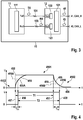
- Fig. 3 the structure of an ECU (electronic control unit) or a control device 15 of a subscriber station 10, 30 is shown.
- the communication control device 11 or protocol controller has an evaluation unit 111 and connections TxD, RxD for a TxD signal line and an RxD signal line.
- the transmitting / receiving device 12 has a receiving level adjustment unit 121 and also connections TxD, RxD for the TxD signal line and the RxD signal line.
- a TxD driver 122 is provided at the connection TxD, which driver actively drives the level of the transmission signal TX received by the communication control device 11 to a predetermined level.
- an RxD driver 123 is provided, which actively drives the level of the received signal RX to a predetermined level for transmission to the communication control device 11.
- the TxD signal line for the transmission signal TX is thus connected to TxD connections of the communication control device 11 and the transmission / reception device 12.
- the RxD signal line for the received signal RX is connected to RxD connections of the communication control device 11 and the transceiver device 12.
- the TxD signal line has at least a resistor 151 connected in series.
- at least one resistor 155 is connected in series in the RxD signal line.
- the communication control device 11 or protocol controller sends data in the form of the transmission signal TX for a message 45, for example, via the TxD signal line to the transmitting / receiving device 12 Message 45 on bus lines 41, 42 or CAN_H and CAN_L.
- a message 47 that was received by the transmitting / receiving device 12 via the bus lines 41, 42 or CAN_H and CAN_L is converted by the transmitting / receiving device 12 as data in the form of the received signal RX and sent to it via the RxD signal line the communication control device 11 is forwarded.
- the at least one resistor 151 additionally built into the TxD signal line has a positive effect on the CAN FD bit timings of the signal on the TxD signal line.
- the at least one resistor 155 additionally built into the RxD signal line has a positive influence on the CAN FD bit timings of the signal on the RxD signal line.
- Fig. 4 the upper part shows the RxD signal or received signal RX at the ⁇ C input (pin) or the control control device 11 with and without filtering with the respective resistor 151, 155.
- the lower part of FIG Fig. 4 shows the received signal present in the control control device 11 at the output of the internal scanning unit in the evaluation unit 111.
- bits 455, 456 with the recessive bus state 4501 are each preceded by a dominant bus state 4502 and the recessive bits 455, 456 are followed by a dominant bus state 4502 an almost rectangular waveform.
- a state change between the dominant bus state 4502 and the recessive bus state 4501 takes place with almost no time delay.
- the bit 455 in the received signal has RX at the RxD connection of the control control device 11 from Fig. 3 a course in which the state change from the dominant bus state 4502 to the recessive bus state 4501 rises slowly from the dominant bus state 4502 and thus reaches the recessive bus state 4501 after a certain time delay.
- the bit reaches 455 due to the resistor 155 after a state change from the dominant bus state 4502 to the recessive bus state 4501 in FIG Fig. 4
- the introduction of the circuit with the resistor 155 in cooperation with a parasitic capacitance of the line between the RxD connections results in an RC behavior on the signal lines between the control control device 11 and the transceiver device 12.
- the evaluation unit 111 shifts the reception level at the input of the control control device 11, that is to say at the connection RxD of the control control device 11, for a rising edge of the signal RX from the voltage level 456A to the voltage level 455A and for a falling edge of the signal RX from the voltage level 456B to the voltage level 455B.
- This can be carried out, for example, by appropriate programming of the control control device 11 with the evaluation unit 111.
- the monitoring control device 11 scans the bit 455 and thus the received signal RX no longer with the conventional scanning period T1 for a recessive bit 456, but with an extended period T2.
- the time period T2 begins later than the conventional sampling period T1 by a predetermined time period T V1 or is delayed in time by a delay period T V1.
- the time period T2 ends a predetermined time period T V2 later than the conventional sampling period T1.
- the end point in time of the sampling is thus also delayed in time by a delay period T V2.
- the delay period T V1 is shorter than the delay period T V2 .
- the resistor 151 is present in the TxD signal line.
- the receiving level adjustment unit 121 shifts the receiving level at the input of the transmitting / receiving device 12, that is to say at the connection TxD of the transmitting / receiving device 12, from the voltage level 456A to the voltage level 455A and from the voltage level 456B to the voltage level 455B.
- This can also be carried out, for example, by appropriate programming of the transmitting / receiving device 12 with the receiving level adjustment unit 121.
- the parameter tbit_rxd of the specification ISO11898-2: 2016 also changes.
- the resistors 151, 155 are designed in such a way that the time delay caused by the individual bits 455 of the CAN frame or CAN FD frame of a message 45 is not so great that the requirement of the propagation delay time according to the CAN specification ISO11898- 2: 2016 cannot be met.
- the propagation delay time according to the CAN specification ISO11898-2: 2016 is a maximum of 255ns from the TxD connection of the communication control device 11 to the bus 40 and from there back via the RxD connection to the communication control device 11.
- a time delay is introduced in the signal line for the signal between the TxD connections depending on the bus status on bus 40.
- a time delay is introduced in the signal line for the signal between the RxD connections.
- the delay introduced into the signal line between the TxD connections may differ from the delay introduced into the signal line between the RxD connections.
- the resistance value of at least one of the resistors 151, 155 can be set on the bus 40 as a function of the bus state.
- the resistor 151 is reduced. If, for example, it is determined as the bus state that the parameter Tbit_bus is in the permissible value range, but Tbit_rxd is too small, then the resistor 155 is increased. If, on the other hand, it is determined as the bus state that the parameter Tbit_bus is in the permissible value range, but Tbit_rxd is too large, then the resistor 155 is reduced.
- the setting of the resistance value can in particular be carried out with the evaluation unit 111 and / or the reception level setting unit 121.
- the previously described delay of the state change or rising or falling edges of the signal can be set as a function of the respective bus state.
- the transmitting / receiving device 12 in particular the receiving level adjustment unit 121, in a further modification of the circuit of FIG Fig. 3 also designed to shift the bus level of the TxD driver 122 and / or of the RxD driver 123 accordingly.
- the bus level of the TxD driver can differ from the bus level of the RxD driver.
- the transmitting / receiving device 12 in particular the receiving level adjustment unit 121, is also designed to provide an additional delay in the state change or rising or falling edges of the signal to the TX signal at the TxD connection and / or to the RX signal at the RxD Connection to be introduced depending on the respective bus status.
- the delay that is introduced into the TX signal can be different from the delay that is introduced into the RX signal.
- the communication control device 11 in particular the evaluation unit 111, is also designed to introduce an additional delay in the state change or rising or falling edges of the signal depending on the respective bus state.
- the delay that is introduced into the TX signal can differ from the delay that is introduced into the RX signal.
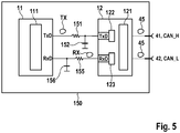
- Fig. 5 illustrates a control unit 150 according to a second embodiment.
- capacitors 152, 156 each with a predetermined capacitance are provided here.
- the resistor 151 and the capacitor 152 form an RC element in the signal line between the terminals TxD.
- the resistor 155 and the capacitor 156 form an RC element in the signal line between the connections RxD.
- the capacitance of the capacitor 152 also interacts with the parasitic capacitance of the line between the TxD connections.
- the capacitance of capacitor 156 interacts with the parasitic capacitance of the line between the RxD terminals.
- the time delay of the transmission signal TX and / or the reception signal RX can be further optimized in comparison to the control unit 15 for improving the bit timing.
- At least one of the capacitors 152, 156 is preferably adjustable with regard to its capacitance value.
- the setting can be carried out in particular by connecting or disconnecting the desired capacitor 152, 156 with a switch.
- the bus status can be, for example, that the minimum value or the maximum value according to, for example, table 13 of the above-mentioned specification ISO11898-2: 2016 for at least one of the above-mentioned parameters is not complied with. If, for example, it is determined as the bus state that the parameter Tbit_bus is too small, then the resistor 151 and / or the capacitor 152 is increased. If, on the other hand, it is determined as the bus state that the parameter Tbit_bus is too large, then the resistor 151 and / or the capacitor 152 is reduced.
- control units 15, 150 The method described with the control units 15, 150 is based on a signal according to FIG Fig. 4 in which a single recessive bit 455 is preceded and followed by a dominant phase or a dominant bus state 4502. It is of course also possible for the dominant and / or the recessive phase to include one or more bits.
- the above-described bus system 1 according to the first to third exemplary embodiments is described using a bus system based on the CAN protocol.
- the bus system 1 according to the first to third exemplary embodiments can, however, also be a different type of communication network. It is advantageous, but not a mandatory prerequisite, that the bus system 1 has an exclusive, collision-free one at least for certain periods of time Access of a subscriber station 10, 20, 30 to the bus line 40 or a common channel of the bus line 40 is guaranteed.
- the bus system 1 is in particular a CAN network or a CAN FD network or a FlexRay network.
- the number and arrangement of the subscriber stations 10, 20, 30 in the bus systems 1 according to the first to third exemplary embodiments is arbitrary. In particular, only subscriber stations 10 or subscriber stations 30 can also be present in the bus systems 1 of the first to third exemplary embodiments.
- the data transmission can take place within the CAN frame of the messages 45, 46, 47 analogous to data transmission protocols such as Ethernet, etc.
Landscapes
- Engineering & Computer Science (AREA)
- Computer Networks & Wireless Communication (AREA)
- Signal Processing (AREA)
- Small-Scale Networks (AREA)
- Dc Digital Transmission (AREA)
Claims (10)
- Poste d'utilisateur (10 ; 30) pour un système de bus (1), comprenant
un dispositif d'émission/réception (12) pour émettre ou recevoir un message (45 ; 46 ; 47) à destination/ en provenance d'au moins un autre poste d'utilisateur du système de bus (1) par le système de bus (1), système de bus (1) dans lequel un accès exclusif, sans collision, d'un poste d'utilisateur (10, 20, 30) à un bus (40) du système de bus (1) est garanti au moins temporairement, et
un dispositif de commande de communication (11) pour créer le message (45 ; 46 ; 47) à émettre par le dispositif d'émission/réception (12) ou pour lire le message (45 ; 46 ; 47) reçu par le dispositif d'émission/réception (12) selon un protocole de communication prédéterminé pour le système de bus (1), et
une unité de temporisation qui est couplée entre le dispositif de commande de communication (11) et le dispositif d'émission/réception (12) pour temporiser un signal d'émission (TX) émis par le dispositif de commande de communication (11) au dispositif d'émission/réception (12) et un signal de réception (RX) reçu par le dispositif d'émission/réception (12). - Poste d'utilisateur (10 ; 30) selon la revendication 1, l'unité de temporisation présentant au moins une résistance (151 ; 155) formant avec une capacité un circuit RC qui est couplé entre le dispositif de commande de communication (11) et le dispositif d'émission/réception (12), et
une unité (111 ; 121) qui est conçue pour retarder dans le temps d'une première valeur prédéterminée (TV1) un seuil de réception pour un signal reçu (TX ; RX) pour un flanc montant du signal (TX ; RX) et pour l'abaisser d'un niveau de tension précédent (456A) à un niveau de tension inférieur (455A), et pour le retarder dans le temps d'une deuxième valeur prédéterminée (TV2) pour un flanc descendant du signal (TX ; RX) et pour l'abaisser d'un niveau de tension précédent (456B) à un niveau de tension inférieur (455B). - Poste d'utilisateur (10 ; 30) selon la revendication 2, dans lequel la capacité est une capacité parasite de la ligne de signal entre le dispositif de commande de communication (11) et le dispositif d'émission/réception (12) ou présente en outre une capacité d'un condensateur (152 ; 156) qui est interconnectée comme circuit RC avec la résistance (151 ; 155).
- Poste d'utilisateur (10 ; 30) selon la revendication 2 ou 3, dans lequel ladite au moins une résistance (151) est couplée entre une borne (TxD) du dispositif de commande de communication (11), qui est prévue pour un signal d'émission (TX) à émettre par le dispositif de commande de communication (11), et une borne (TxD) du dispositif d'émission/réception (12), qui est prévue pour le signal d'émission (TX) émis par le dispositif de commande de communication (11).
- Poste d'utilisateur (10 ; 30) selon la revendication 3 ou 4, dans lequel le condensateur (152) est relié au niveau d'une de ses bornes à ladite au moins une résistance (151) et à la borne (TxD) du dispositif d'émission/réception (12) pour un signal d'émission (TX) émis par le dispositif de commande de communication (11) et est relié à la masse au niveau de son autre borne.
- Poste d'utilisateur (10 ; 30) selon l'une quelconque des revendications précédentes, dans lequel ladite au moins une résistance (155) est couplée entre une borne (RxD) du dispositif d'émission/réception (12) qui est prévue pour un signal de réception (RX) reçu du bus par le dispositif d'émission/réception (12), et une borne (RxD) du dispositif de commande de communication (11) qui est prévue pour un signal de réception reçu du bus par le dispositif d'émission/réception (12).
- Poste d'utilisateur (10 ; 30) selon la revendication 6, dans lequel le condensateur (156) est relié au niveau d'une de ses bornes à ladite au moins une résistance (155) et à la borne (RxD) du dispositif de commande de communication (11) pour un signal de réception (RX) reçu par le dispositif d'émission/réception (12), et est relié à la masse au niveau de son autre borne.
- Poste d'utilisateur (10 ; 30) selon l'une quelconque des revendications précédentes, dans lequel l'unité de temporisation est conçue pour introduire la temporisation en fonction de l'état du bus, et/ou le dispositif d'émission/réception (12) présente une unité (121) qui est conçue pour retarder dans le temps le signal (CAN_H, CAN_L) à émettre sur le bus (40) en fonction de l'état du bus, et/ou
le dispositif de commande de communication (11) présente une unité qui est conçue pour retarder dans le temps le signal d'émission (TX) ou le signal de réception (RX) reçu par le dispositif d'émission/réception (12) du bus (40) en fonction de l'état du bus, et/ou
le dispositif d'émission/réception (12) présente une unité (121) qui est conçue pour abaisser le niveau de bus d'un pilote TxD (122) et/ou d'un pilote RxD (123). - Système de bus (1), comprenant
un bus (40), et
au moins deux postes d'utilisateur (10 ; 20 ; 30) qui sont reliés l'un à l'autre par le bus (4) de telle sorte qu'ils peuvent communiquer l'un avec l'autre, caractérisé en ce qu'au moins l'un des au moins deux postes d'utilisateur (10 ; 20 ; 30) est un poste d'utilisateur (10 ; 30) selon l'une quelconque des revendications précédentes. - Procédé d'amélioration du respect de la condition de synchronisation binaire dans un système de bus (1), dans lequel un accès exclusif, sans collision, d'un poste d'utilisateur (10, 20, 30) à un bus (40) du système de bus (1) est garanti au moins temporairement, le poste d'utilisateur présentant un dispositif d'émission/réception (12) pour émettre ou recevoir un message (45 ; 46 ; 47) à destination/en provenance d'au moins un autre poste d'utilisateur du système de bus (1) par le système de bus (1), et un dispositif de commande de communication (11) pour créer le message (45 ; 46 ; 47) à émettre par le dispositif d'émission/réception (12) ou pour lire le message (45 ; 46 ; 47) reçu par le dispositif d'émission/réception (12) selon un protocole de communication prédéterminé pour le système de bus (1), et
le procédé présentant l'étape consistant à
temporiser, par une unité de temporisation, qui est couplée entre le dispositif de commande de communication (11) et le dispositif d'émission/réception (12), un signal d'émission (TX) émis par le dispositif de commande de communication (11) au dispositif d'émission/réception (12) et un signal de réception (RX) reçu par le dispositif d'émission/réception (12).
Applications Claiming Priority (2)
| Application Number | Priority Date | Filing Date | Title |
|---|---|---|---|
| DE102017205785.8A DE102017205785A1 (de) | 2017-04-05 | 2017-04-05 | Teilnehmerstation für ein Bussystem und Verfahren zur Verbesserung der Einhaltung der Bit-Timing-Anforderung in einem Bussystem |
| PCT/EP2018/058415 WO2018185064A1 (fr) | 2017-04-05 | 2018-04-03 | Station d'abonné pour un système de bus et procédé d'amélioration du respect de l'exigence de rythme des bits dans un système de bus |
Publications (2)
| Publication Number | Publication Date |
|---|---|
| EP3607703A1 EP3607703A1 (fr) | 2020-02-12 |
| EP3607703B1 true EP3607703B1 (fr) | 2021-08-11 |
Family
ID=61911579
Family Applications (1)
| Application Number | Title | Priority Date | Filing Date |
|---|---|---|---|
| EP18716199.7A Active EP3607703B1 (fr) | 2017-04-05 | 2018-04-03 | Station d'abonné pour un système de bus et procédé d'amélioration du respect de l'exigence de rythme des bits dans un système de bus |
Country Status (4)
| Country | Link |
|---|---|
| EP (1) | EP3607703B1 (fr) |
| CN (1) | CN110679116B (fr) |
| DE (1) | DE102017205785A1 (fr) |
| WO (1) | WO2018185064A1 (fr) |
Families Citing this family (6)
| Publication number | Priority date | Publication date | Assignee | Title |
|---|---|---|---|---|
| DE102018221957A1 (de) * | 2018-12-17 | 2020-06-18 | Robert Bosch Gmbh | Einrichtung für eine Teilnehmerstation eines seriellen Bussystems und Verfahren zur Kommunikation in einem seriellen Bussystem |
| US10778481B1 (en) | 2019-03-25 | 2020-09-15 | Delphi Technologies Ip Limited | Adaptable can transceiver and system |
| DE102019208059A1 (de) * | 2019-06-03 | 2020-12-03 | Robert Bosch Gmbh | Einrichtung für eine Teilnehmerstation eines seriellen Bussystems und Verfahren zur Kommunikation in einem seriellen Bussystem |
| DE102020200802A1 (de) * | 2020-01-23 | 2021-07-29 | Robert Bosch Gesellschaft mit beschränkter Haftung | Sende-/Empfangseinrichtung und Kommunikationssteuereinrichtung für eine Teilnehmerstation eines seriellen Bussystems und Verfahren zur Kommunikation in einem seriellen Bussystem |
| DE102020200804A1 (de) * | 2020-01-23 | 2021-07-29 | Robert Bosch Gesellschaft mit beschränkter Haftung | Sende-/Empfangseinrichtung und Kommunikationssteuereinrichtung für eine Teilnehmerstation eines seriellen Bussystems und Verfahren zur Kommunikation in einem seriellen Bussystem |
| DE102021207188A1 (de) * | 2021-07-08 | 2023-01-12 | Robert Bosch Gesellschaft mit beschränkter Haftung | Empfangsmodul und Verfahren zum Empfangen von differentiellen Signalen in einem seriellen Bussystem |
Family Cites Families (8)
| Publication number | Priority date | Publication date | Assignee | Title |
|---|---|---|---|---|
| DE10000305B4 (de) | 2000-01-05 | 2011-08-11 | Robert Bosch GmbH, 70469 | Verfahren und Vorrichtung zum Austausch von Daten zwischen wenigstens zwei mit einem Bussystem verbundenen Teilnehmern |
| US7778599B2 (en) * | 2006-05-01 | 2010-08-17 | Intel Corporation | Aggregated channel feedback |
| DE102009026965A1 (de) * | 2009-06-16 | 2010-12-23 | Robert Bosch Gmbh | Medienzugriffssteuerverfahren für ein Bussystem und Kommunikationseinrichtung |
| DE102012200997A1 (de) | 2011-08-29 | 2013-02-28 | Robert Bosch Gmbh | Verfahren und Vorrichtung zur Prüfung der korrekten Funktion einer seriellen Datenübertragung |
| DE102011089587A1 (de) * | 2011-12-22 | 2013-06-27 | Robert Bosch Gmbh | Teilnehmerstation eines Bussystems und Verfahren zur Übertragung von Nachrichten zwischen Teilnehmerstationen eines Bussystems |
| DE102014204050A1 (de) * | 2014-03-05 | 2015-09-10 | Robert Bosch Gmbh | Teilnehmerstation für ein Bussystem und Verfahren zur Verbesserung der Sendequalität in einem Bussystem |
| DE102014223838A1 (de) * | 2014-11-21 | 2016-05-25 | Robert Bosch Gmbh | Teilnehmerstation für ein Bussystem und ein Verfahren zum Regeln eines Timings eines Sendesignals für ein Bussystem |
| EP3319274B1 (fr) * | 2016-11-02 | 2019-04-17 | NXP USA, Inc. | Module de bus can et procédé associé |
-
2017
- 2017-04-05 DE DE102017205785.8A patent/DE102017205785A1/de not_active Withdrawn
-
2018
- 2018-04-03 WO PCT/EP2018/058415 patent/WO2018185064A1/fr unknown
- 2018-04-03 EP EP18716199.7A patent/EP3607703B1/fr active Active
- 2018-04-03 CN CN201880037113.5A patent/CN110679116B/zh active Active
Also Published As
| Publication number | Publication date |
|---|---|
| WO2018185064A1 (fr) | 2018-10-11 |
| DE102017205785A1 (de) | 2018-10-11 |
| CN110679116A (zh) | 2020-01-10 |
| CN110679116B (zh) | 2021-11-26 |
| EP3607703A1 (fr) | 2020-02-12 |
Similar Documents
| Publication | Publication Date | Title |
|---|---|---|
| EP3607703B1 (fr) | Station d'abonné pour un système de bus et procédé d'amélioration du respect de l'exigence de rythme des bits dans un système de bus | |
| EP3114800B1 (fr) | Station d'abonné pour un système de bus et procédé d'amélioration de la qualité d'émission dans un système de bus | |
| EP3114801B1 (fr) | Station d'abonné pour un système de bus et procédé de réduction d'émissions liées à une ligne dans un système de bus | |
| EP2443557B1 (fr) | Dispositif de transmission de données entre des stations utilisateurs d'un système de bus | |
| EP2443797B1 (fr) | Procédé de commande d'accès à un support pour un système de bus et dispositif de communication | |
| EP2619948B1 (fr) | Procédé et station d'abonné pour la transmission optimisée de données entre les stations d'abonné d'un système de bus | |
| WO2015014550A1 (fr) | Poste d'abonné pour un système de bus et procédé pour améliorer la robustesse aux erreurs d'un poste d'abonné d'un système de bus | |
| DE102005037263A1 (de) | Verfahren und Vorrichtung zum Decodieren eines Signals | |
| EP3665872B1 (fr) | Unité de réduction d'oscillation pour système de bus et procédé de réduction de la tendance à osciller lors de la transition entre différentes états binaires | |
| EP3665870A1 (fr) | Dispositif d'émission / réception pour un système de bus et procédé de réduction d'une disposition aux oscillations lors de la transition entre différents états binaires | |
| EP3756311B1 (fr) | Dispositif et procédé destinés à un moyen émetteur-récepteur d'un système de bus | |
| EP3665874B1 (fr) | Dispositif d'émission/réception pour systeme de bus et procédé de réduction de la tendance à osciller lors de la transition entre différents état binaires | |
| WO2020035392A1 (fr) | Unité de blindage de trame, station d'abonnés pour un système de bus série et procédé de communication dans un système de bus série | |
| DE102019205488A1 (de) | Teilnehmerstation für ein serielles Bussystem und Verfahren zur Kommunikation in einem seriellen Bussystem | |
| EP2534582B1 (fr) | Circuit d'un genre nouveau et procédé de communication par le biais d'une ligne unique | |
| EP3665869A1 (fr) | Dispositif d'émission/réception pour systeme de bus et procédé de réduction de la tendance à osciller entre differents états binaires | |
| DE102021207188A1 (de) | Empfangsmodul und Verfahren zum Empfangen von differentiellen Signalen in einem seriellen Bussystem | |
| WO2023280474A1 (fr) | Module d'émission et procédé d'émission de signaux différentiels dans un système de bus série | |
| WO2024037766A1 (fr) | Module d'interface pour une station d'abonné d'un système de bus série et procédé de transmission d'un message dans un système de bus série | |
| DE102020214649A1 (de) | Teilnehmerstation für ein serielles Bussystem und Verfahren zur Kommunikation in einem seriellen Bussystem | |
| WO2020244986A1 (fr) | Station d'abonné pour un système de bus série et procédé de communication dans un système de bus série |
Legal Events
| Date | Code | Title | Description |
|---|---|---|---|
| STAA | Information on the status of an ep patent application or granted ep patent |
Free format text: STATUS: UNKNOWN |
|
| STAA | Information on the status of an ep patent application or granted ep patent |
Free format text: STATUS: THE INTERNATIONAL PUBLICATION HAS BEEN MADE |
|
| PUAI | Public reference made under article 153(3) epc to a published international application that has entered the european phase |
Free format text: ORIGINAL CODE: 0009012 |
|
| STAA | Information on the status of an ep patent application or granted ep patent |
Free format text: STATUS: REQUEST FOR EXAMINATION WAS MADE |
|
| 17P | Request for examination filed |
Effective date: 20191105 |
|
| AK | Designated contracting states |
Kind code of ref document: A1 Designated state(s): AL AT BE BG CH CY CZ DE DK EE ES FI FR GB GR HR HU IE IS IT LI LT LU LV MC MK MT NL NO PL PT RO RS SE SI SK SM TR |
|
| AX | Request for extension of the european patent |
Extension state: BA ME |
|
| RAP1 | Party data changed (applicant data changed or rights of an application transferred) |
Owner name: ROBERT BOSCH GMBH |
|
| DAV | Request for validation of the european patent (deleted) | ||
| DAX | Request for extension of the european patent (deleted) | ||
| GRAP | Despatch of communication of intention to grant a patent |
Free format text: ORIGINAL CODE: EPIDOSNIGR1 |
|
| STAA | Information on the status of an ep patent application or granted ep patent |
Free format text: STATUS: GRANT OF PATENT IS INTENDED |
|
| INTG | Intention to grant announced |
Effective date: 20210601 |
|
| GRAS | Grant fee paid |
Free format text: ORIGINAL CODE: EPIDOSNIGR3 |
|
| GRAA | (expected) grant |
Free format text: ORIGINAL CODE: 0009210 |
|
| STAA | Information on the status of an ep patent application or granted ep patent |
Free format text: STATUS: THE PATENT HAS BEEN GRANTED |
|
| AK | Designated contracting states |
Kind code of ref document: B1 Designated state(s): AL AT BE BG CH CY CZ DE DK EE ES FI FR GB GR HR HU IE IS IT LI LT LU LV MC MK MT NL NO PL PT RO RS SE SI SK SM TR |
|
| REG | Reference to a national code |
Ref country code: CH Ref legal event code: EP |
|
| REG | Reference to a national code |
Ref country code: DE Ref legal event code: R096 Ref document number: 502018006534 Country of ref document: DE |
|
| REG | Reference to a national code |
Ref country code: NL Ref legal event code: FP |
|
| REG | Reference to a national code |
Ref country code: IE Ref legal event code: FG4D Free format text: LANGUAGE OF EP DOCUMENT: GERMAN Ref country code: AT Ref legal event code: REF Ref document number: 1420522 Country of ref document: AT Kind code of ref document: T Effective date: 20210915 |
|
| REG | Reference to a national code |
Ref country code: LT Ref legal event code: MG9D |
|
| PG25 | Lapsed in a contracting state [announced via postgrant information from national office to epo] |
Ref country code: LT Free format text: LAPSE BECAUSE OF FAILURE TO SUBMIT A TRANSLATION OF THE DESCRIPTION OR TO PAY THE FEE WITHIN THE PRESCRIBED TIME-LIMIT Effective date: 20210811 Ref country code: BG Free format text: LAPSE BECAUSE OF FAILURE TO SUBMIT A TRANSLATION OF THE DESCRIPTION OR TO PAY THE FEE WITHIN THE PRESCRIBED TIME-LIMIT Effective date: 20211111 Ref country code: NO Free format text: LAPSE BECAUSE OF FAILURE TO SUBMIT A TRANSLATION OF THE DESCRIPTION OR TO PAY THE FEE WITHIN THE PRESCRIBED TIME-LIMIT Effective date: 20211111 Ref country code: PT Free format text: LAPSE BECAUSE OF FAILURE TO SUBMIT A TRANSLATION OF THE DESCRIPTION OR TO PAY THE FEE WITHIN THE PRESCRIBED TIME-LIMIT Effective date: 20211213 Ref country code: HR Free format text: LAPSE BECAUSE OF FAILURE TO SUBMIT A TRANSLATION OF THE DESCRIPTION OR TO PAY THE FEE WITHIN THE PRESCRIBED TIME-LIMIT Effective date: 20210811 Ref country code: ES Free format text: LAPSE BECAUSE OF FAILURE TO SUBMIT A TRANSLATION OF THE DESCRIPTION OR TO PAY THE FEE WITHIN THE PRESCRIBED TIME-LIMIT Effective date: 20210811 Ref country code: FI Free format text: LAPSE BECAUSE OF FAILURE TO SUBMIT A TRANSLATION OF THE DESCRIPTION OR TO PAY THE FEE WITHIN THE PRESCRIBED TIME-LIMIT Effective date: 20210811 Ref country code: SE Free format text: LAPSE BECAUSE OF FAILURE TO SUBMIT A TRANSLATION OF THE DESCRIPTION OR TO PAY THE FEE WITHIN THE PRESCRIBED TIME-LIMIT Effective date: 20210811 Ref country code: RS Free format text: LAPSE BECAUSE OF FAILURE TO SUBMIT A TRANSLATION OF THE DESCRIPTION OR TO PAY THE FEE WITHIN THE PRESCRIBED TIME-LIMIT Effective date: 20210811 |
|
| PG25 | Lapsed in a contracting state [announced via postgrant information from national office to epo] |
Ref country code: PL Free format text: LAPSE BECAUSE OF FAILURE TO SUBMIT A TRANSLATION OF THE DESCRIPTION OR TO PAY THE FEE WITHIN THE PRESCRIBED TIME-LIMIT Effective date: 20210811 Ref country code: LV Free format text: LAPSE BECAUSE OF FAILURE TO SUBMIT A TRANSLATION OF THE DESCRIPTION OR TO PAY THE FEE WITHIN THE PRESCRIBED TIME-LIMIT Effective date: 20210811 Ref country code: GR Free format text: LAPSE BECAUSE OF FAILURE TO SUBMIT A TRANSLATION OF THE DESCRIPTION OR TO PAY THE FEE WITHIN THE PRESCRIBED TIME-LIMIT Effective date: 20211112 |
|
| PG25 | Lapsed in a contracting state [announced via postgrant information from national office to epo] |
Ref country code: DK Free format text: LAPSE BECAUSE OF FAILURE TO SUBMIT A TRANSLATION OF THE DESCRIPTION OR TO PAY THE FEE WITHIN THE PRESCRIBED TIME-LIMIT Effective date: 20210811 |
|
| REG | Reference to a national code |
Ref country code: DE Ref legal event code: R097 Ref document number: 502018006534 Country of ref document: DE |
|
| PG25 | Lapsed in a contracting state [announced via postgrant information from national office to epo] |
Ref country code: SM Free format text: LAPSE BECAUSE OF FAILURE TO SUBMIT A TRANSLATION OF THE DESCRIPTION OR TO PAY THE FEE WITHIN THE PRESCRIBED TIME-LIMIT Effective date: 20210811 Ref country code: SK Free format text: LAPSE BECAUSE OF FAILURE TO SUBMIT A TRANSLATION OF THE DESCRIPTION OR TO PAY THE FEE WITHIN THE PRESCRIBED TIME-LIMIT Effective date: 20210811 Ref country code: RO Free format text: LAPSE BECAUSE OF FAILURE TO SUBMIT A TRANSLATION OF THE DESCRIPTION OR TO PAY THE FEE WITHIN THE PRESCRIBED TIME-LIMIT Effective date: 20210811 Ref country code: EE Free format text: LAPSE BECAUSE OF FAILURE TO SUBMIT A TRANSLATION OF THE DESCRIPTION OR TO PAY THE FEE WITHIN THE PRESCRIBED TIME-LIMIT Effective date: 20210811 Ref country code: CZ Free format text: LAPSE BECAUSE OF FAILURE TO SUBMIT A TRANSLATION OF THE DESCRIPTION OR TO PAY THE FEE WITHIN THE PRESCRIBED TIME-LIMIT Effective date: 20210811 Ref country code: AL Free format text: LAPSE BECAUSE OF FAILURE TO SUBMIT A TRANSLATION OF THE DESCRIPTION OR TO PAY THE FEE WITHIN THE PRESCRIBED TIME-LIMIT Effective date: 20210811 |
|
| PLBE | No opposition filed within time limit |
Free format text: ORIGINAL CODE: 0009261 |
|
| STAA | Information on the status of an ep patent application or granted ep patent |
Free format text: STATUS: NO OPPOSITION FILED WITHIN TIME LIMIT |
|
| 26N | No opposition filed |
Effective date: 20220512 |
|
| PG25 | Lapsed in a contracting state [announced via postgrant information from national office to epo] |
Ref country code: SI Free format text: LAPSE BECAUSE OF FAILURE TO SUBMIT A TRANSLATION OF THE DESCRIPTION OR TO PAY THE FEE WITHIN THE PRESCRIBED TIME-LIMIT Effective date: 20210811 |
|
| REG | Reference to a national code |
Ref country code: CH Ref legal event code: PL |
|
| GBPC | Gb: european patent ceased through non-payment of renewal fee |
Effective date: 20220403 |
|
| REG | Reference to a national code |
Ref country code: BE Ref legal event code: MM Effective date: 20220430 |
|
| PG25 | Lapsed in a contracting state [announced via postgrant information from national office to epo] |
Ref country code: MC Free format text: LAPSE BECAUSE OF FAILURE TO SUBMIT A TRANSLATION OF THE DESCRIPTION OR TO PAY THE FEE WITHIN THE PRESCRIBED TIME-LIMIT Effective date: 20210811 Ref country code: LU Free format text: LAPSE BECAUSE OF NON-PAYMENT OF DUE FEES Effective date: 20220403 Ref country code: LI Free format text: LAPSE BECAUSE OF NON-PAYMENT OF DUE FEES Effective date: 20220430 Ref country code: GB Free format text: LAPSE BECAUSE OF NON-PAYMENT OF DUE FEES Effective date: 20220403 Ref country code: CH Free format text: LAPSE BECAUSE OF NON-PAYMENT OF DUE FEES Effective date: 20220430 |
|
| PG25 | Lapsed in a contracting state [announced via postgrant information from national office to epo] |
Ref country code: BE Free format text: LAPSE BECAUSE OF NON-PAYMENT OF DUE FEES Effective date: 20220430 |
|
| PG25 | Lapsed in a contracting state [announced via postgrant information from national office to epo] |
Ref country code: IE Free format text: LAPSE BECAUSE OF NON-PAYMENT OF DUE FEES Effective date: 20220403 |
|
| PGFP | Annual fee paid to national office [announced via postgrant information from national office to epo] |
Ref country code: IT Payment date: 20230428 Year of fee payment: 6 Ref country code: FR Payment date: 20230417 Year of fee payment: 6 Ref country code: DE Payment date: 20230627 Year of fee payment: 6 |
|
| PG25 | Lapsed in a contracting state [announced via postgrant information from national office to epo] |
Ref country code: MK Free format text: LAPSE BECAUSE OF FAILURE TO SUBMIT A TRANSLATION OF THE DESCRIPTION OR TO PAY THE FEE WITHIN THE PRESCRIBED TIME-LIMIT Effective date: 20210811 Ref country code: CY Free format text: LAPSE BECAUSE OF FAILURE TO SUBMIT A TRANSLATION OF THE DESCRIPTION OR TO PAY THE FEE WITHIN THE PRESCRIBED TIME-LIMIT Effective date: 20210811 |
|
| PGFP | Annual fee paid to national office [announced via postgrant information from national office to epo] |
Ref country code: NL Payment date: 20240422 Year of fee payment: 7 |