EP3607703B1 - Subscriber station for a bus system and method for improving the compliance with the bit-timing request in a bus system - Google Patents
Subscriber station for a bus system and method for improving the compliance with the bit-timing request in a bus system Download PDFInfo
- Publication number
- EP3607703B1 EP3607703B1 EP18716199.7A EP18716199A EP3607703B1 EP 3607703 B1 EP3607703 B1 EP 3607703B1 EP 18716199 A EP18716199 A EP 18716199A EP 3607703 B1 EP3607703 B1 EP 3607703B1
- Authority
- EP
- European Patent Office
- Prior art keywords
- transmission
- bus
- reception device
- control device
- signal
- Prior art date
- Legal status (The legal status is an assumption and is not a legal conclusion. Google has not performed a legal analysis and makes no representation as to the accuracy of the status listed.)
- Active
Links
Images

Classifications
-
- H—ELECTRICITY
- H04—ELECTRIC COMMUNICATION TECHNIQUE
- H04L—TRANSMISSION OF DIGITAL INFORMATION, e.g. TELEGRAPHIC COMMUNICATION
- H04L12/00—Data switching networks
- H04L12/28—Data switching networks characterised by path configuration, e.g. LAN [Local Area Networks] or WAN [Wide Area Networks]
- H04L12/40—Bus networks
- H04L12/40006—Architecture of a communication node
-
- H—ELECTRICITY
- H04—ELECTRIC COMMUNICATION TECHNIQUE
- H04L—TRANSMISSION OF DIGITAL INFORMATION, e.g. TELEGRAPHIC COMMUNICATION
- H04L12/00—Data switching networks
- H04L12/28—Data switching networks characterised by path configuration, e.g. LAN [Local Area Networks] or WAN [Wide Area Networks]
- H04L12/40—Bus networks
- H04L2012/40208—Bus networks characterized by the use of a particular bus standard
- H04L2012/40215—Controller Area Network CAN
Definitions
- the present invention relates to a subscriber station for a bus system and a method for improving compliance with the bit timing requirement in a bus system in order to achieve good reception quality even with a possible asymmetry of received bits at high data rates.
- a classic CAN frame is divided into an arbitration field and a data field.
- bit-by-bit arbitration is used to determine which of the participants in the bus system has exclusive access to a communication medium between the participants in the bus system.
- bit-by-bit arbitration is used to determine which of the participants in the bus system has exclusive access to a communication medium between the participants in the bus system.
- Bitrate_arb Bitrate_data.
- the maximum bit rate is 1 Mbps (mega bits per second), that means the bit time is 1 ⁇ s.
- CAN-FD The CAN protocol was further developed under the name CAN-FD, according to which messages are transmitted according to the specification "CAN with Flexible Data-Rate, Specification Version 1.0" (source http://www.semiconductors.bosch.de). With CAN-FD it is possible to increase the data rate for systems in which the data rate was previously limited by the bus length of the systems.
- bit rate_arb Bitrate_arb ⁇ Bitrate_data applies.
- the disclosure document DE 10 2014 204 050 A1 describes a subscriber station for a bus system one with a transmitting / receiving device for sending or receiving a message, the transmitting / receiving device having a device for processing the transmitted signal of a transmission signal to be transmitted by the transmitting / receiving device.
- This device is designed to set a predetermined bit symmetry of bits of the transmission signal by generating an internal transmission signal for the message, the dominant phase of the bits being shortened and the recessive phase of bits being lengthened in the internal transmission signal.
- the disclosure document DE 10 2014 223 838 A1 describes a subscriber station for a bus system with a detection unit for detecting a bit width of received bits of a message sent via a bus, and a control unit for determining the bit width of at least one bit of a message to be sent in order to meet the bus system requirements for the duty cycle and to regulate the bit width by delaying the edges of a transmission signal on the basis of the detected bit width.
- a subscriber station for a bus system and a method for improving compliance with the bit timing requirement in a bus system which solve the aforementioned problems.
- a subscriber station for a bus system and a method for improving compliance with the bit timing requirement in a bus system are to be provided in which compliance with the bit timing requirements can be met simply, effectively and inexpensively, so that no faulty transmissions appear.
- the object is achieved by a subscriber station for a bus system according to claim 1.
- Compliance with the bit timing requirement of the bus system is achieved through targeted wiring with at least one electrical resistor between the communication control device and the transceiver of an electronic control unit of the subscriber station.
- This makes it possible to migrate an electronic control unit (ECU) of the subscriber station from CAN to CAN-FD without having to exchange the transmitting / receiving device or the transceiver. Because of this, the migration from CAN to CAN-FD can take place without redevelopment of the transmitter / receiver device or the transceiver. This results in a clear cost advantage.
- ECU electronice control unit
- the configuration of the subscriber station described above can also be easily retrofitted to existing subscriber stations. This is particularly advantageous for subscriber stations that would have to be operated in the borderline area with regard to CAN FD bit timing. With the configuration of the subscriber station described above, a greater safety margin can be achieved for the required minimum bit time of an individual bit of the CAN frame. This gives the planner or designer of the bus system, such as a vehicle manufacturer or user, greater degrees of freedom when designing the bus topology and bit rate.
- the delay unit may have at least one resistor that forms an RC element with a capacitance that is connected between the communication control device and the transceiver, and a unit that is designed to provide a reception threshold for a received signal for a rising edge of the To delay the signal by a first predetermined value and to reduce it from a previous voltage level to a lower voltage level and to delay it by a second predetermined value for a falling edge of the signal and to reduce it from a previous voltage level to a lower voltage level.
- the capacitance can be a parasitic capacitance of the signal line between the communication control device and the transmitting / receiving device or also have the capacitance of a capacitor that is connected to the resistor as an RC element.
- the at least one resistor is connected between a connection of the communication control device, which is provided for a transmission signal to be transmitted by the communication control device, and a connection of the transmission / reception device, which is provided for the transmission signal transmitted by the communication control device.
- the capacitor can be connected at its one connection to the at least one resistor and the connection of the transmitting / receiving device for a transmission signal sent by the communication control device and connected to ground at its other connection.
- the at least one resistor is connected between a connection of the transmitting / receiving device, which is provided for a received signal received by the transmitting / receiving device from the bus, and a connection of the communication control device, which is intended for the transmission by the transmitting / receiving device.
- / Receiving device received from the bus is provided.
- the capacitor can be connected at its one connection to the at least one resistor and the connection (RxD) of the communication control device for a received signal received by the transmitting / receiving device and connected to ground at its other connection.
- the delay unit is designed to introduce the delay as a function of the bus state.
- the transmitting / receiving device can have a unit which is designed to delay the signal to be transmitted on the bus in time as a function of the bus state.
- the communication control device can have a unit which is designed to delay the transmission signal to be transmitted or the reception signal received from the bus by the transmission / reception device as a function of the bus status.
- the transmitting / receiving device can have a unit which is designed to reduce the bus level of a TxD driver and / or an RxD driver to belittle. In all of these design variants, compliance with the bit timing requirement of the bus system can be adapted very flexibly to the respective existing conditions.
- the subscriber station described above can be part of a bus system that has a bus and at least two subscriber stations which are connected to one another via the bus in such a way that they can communicate with one another, at least one of the at least two subscriber stations being a previously described subscriber station.
- the aforementioned object is also achieved by a method for improving compliance with the bit timing requirement in a bus system according to claim 10.
- the method offers the same advantages as mentioned above with regard to the subscriber station.
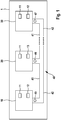
- Fig. 1 shows a bus system 1, which can be a CAN bus system, a CAN FD bus system, etc., for example.
- the bus system 1 can be used in a vehicle, in particular a motor vehicle, an airplane, etc., or in a hospital, etc. use.
- the bus system 1 has a plurality of subscriber stations 10, 20, 30, each of which is connected to a bus 40 with a first bus core 41 and a second bus core 42.
- the bus wires 41, 42 can also be called CAN_H and CAN_L and are used to couple the dominant levels in the transmission state.
- Messages 45, 46, 47 in the form of signals can be transmitted between the individual subscriber stations 10, 20, 30 via bus 40.
- the subscriber stations 10, 20, 30 can be, for example, control devices or display devices of a motor vehicle.
- the subscriber stations 10, 30 each have a communication control device 11 and a transmitting / receiving device 12.
- the subscriber station 20, on the other hand, has a communication control device 11 and a transmitting / receiving device 13.
- the transmitting / receiving devices 12 of the subscriber stations 10, 30 and the transmitter - / receiving device 13 of the subscriber stations 20 are each connected directly to the bus 40, even if this is shown in FIG Fig. 1 is not shown.
- the communication control device 11 is used to control communication between the respective subscriber station 10, 20, 30 via the bus 40 with another subscriber station of the subscriber stations 10, 20, 30 connected to the bus 40 CAN FD controller.
- the transmitting / receiving device 13 of the subscriber station 20 is used to send the messages 46 in the form of a transmit signal TX to another subscriber station of the bus system 1 and to receive the messages 45, 47 from the other subscriber stations of the bus system 1 in the form of a receive signal RX.
- the transmitting / receiving device 13 can be designed like a conventional CAN transceiver.
- Fig. 2 shows in its upper part based on the message 45 a CAN frame as it is sent by the transceiver 12 or the transceiver 13, and in its lower part a CAN FD frame, how it can be sent by the transmitting / receiving device 12.
- the messages 45, 47 are therefore possibly in each case a CAN frame or a CAN FD frame.
- the messages 46 may each be a CAN frame.
- the CAN frame and the CAN FD frame for the CAN communication on the bus 40 are basically divided into two different phases, namely the arbitration phases 451, 453 and a data area 452, which is also the data field for CAN-HS and for CAN -FD is also called data phase.
- the arbitration phases 451, 453 compared to the classic CAN, at the end of the arbitration phase 451 the bit rate for the following data phase is increased to, for example, 2, 4, 5, 8Mbps etc.
- the bit rate in the arbitration phases 451, 453 is lower than the bit rate in the data area 452.
- the data area 452 is significantly shortened compared to the data area 452 of the CAN frame.
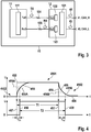
- Fig. 3 the structure of an ECU (electronic control unit) or a control device 15 of a subscriber station 10, 30 is shown.
- the communication control device 11 or protocol controller has an evaluation unit 111 and connections TxD, RxD for a TxD signal line and an RxD signal line.
- the transmitting / receiving device 12 has a receiving level adjustment unit 121 and also connections TxD, RxD for the TxD signal line and the RxD signal line.
- a TxD driver 122 is provided at the connection TxD, which driver actively drives the level of the transmission signal TX received by the communication control device 11 to a predetermined level.
- an RxD driver 123 is provided, which actively drives the level of the received signal RX to a predetermined level for transmission to the communication control device 11.
- the TxD signal line for the transmission signal TX is thus connected to TxD connections of the communication control device 11 and the transmission / reception device 12.
- the RxD signal line for the received signal RX is connected to RxD connections of the communication control device 11 and the transceiver device 12.
- the TxD signal line has at least a resistor 151 connected in series.
- at least one resistor 155 is connected in series in the RxD signal line.
- the communication control device 11 or protocol controller sends data in the form of the transmission signal TX for a message 45, for example, via the TxD signal line to the transmitting / receiving device 12 Message 45 on bus lines 41, 42 or CAN_H and CAN_L.
- a message 47 that was received by the transmitting / receiving device 12 via the bus lines 41, 42 or CAN_H and CAN_L is converted by the transmitting / receiving device 12 as data in the form of the received signal RX and sent to it via the RxD signal line the communication control device 11 is forwarded.
- the at least one resistor 151 additionally built into the TxD signal line has a positive effect on the CAN FD bit timings of the signal on the TxD signal line.
- the at least one resistor 155 additionally built into the RxD signal line has a positive influence on the CAN FD bit timings of the signal on the RxD signal line.
- Fig. 4 the upper part shows the RxD signal or received signal RX at the ⁇ C input (pin) or the control control device 11 with and without filtering with the respective resistor 151, 155.
- the lower part of FIG Fig. 4 shows the received signal present in the control control device 11 at the output of the internal scanning unit in the evaluation unit 111.
- bits 455, 456 with the recessive bus state 4501 are each preceded by a dominant bus state 4502 and the recessive bits 455, 456 are followed by a dominant bus state 4502 an almost rectangular waveform.
- a state change between the dominant bus state 4502 and the recessive bus state 4501 takes place with almost no time delay.
- the bit 455 in the received signal has RX at the RxD connection of the control control device 11 from Fig. 3 a course in which the state change from the dominant bus state 4502 to the recessive bus state 4501 rises slowly from the dominant bus state 4502 and thus reaches the recessive bus state 4501 after a certain time delay.
- the bit reaches 455 due to the resistor 155 after a state change from the dominant bus state 4502 to the recessive bus state 4501 in FIG Fig. 4
- the introduction of the circuit with the resistor 155 in cooperation with a parasitic capacitance of the line between the RxD connections results in an RC behavior on the signal lines between the control control device 11 and the transceiver device 12.
- the evaluation unit 111 shifts the reception level at the input of the control control device 11, that is to say at the connection RxD of the control control device 11, for a rising edge of the signal RX from the voltage level 456A to the voltage level 455A and for a falling edge of the signal RX from the voltage level 456B to the voltage level 455B.
- This can be carried out, for example, by appropriate programming of the control control device 11 with the evaluation unit 111.
- the monitoring control device 11 scans the bit 455 and thus the received signal RX no longer with the conventional scanning period T1 for a recessive bit 456, but with an extended period T2.
- the time period T2 begins later than the conventional sampling period T1 by a predetermined time period T V1 or is delayed in time by a delay period T V1.
- the time period T2 ends a predetermined time period T V2 later than the conventional sampling period T1.
- the end point in time of the sampling is thus also delayed in time by a delay period T V2.
- the delay period T V1 is shorter than the delay period T V2 .
- the resistor 151 is present in the TxD signal line.
- the receiving level adjustment unit 121 shifts the receiving level at the input of the transmitting / receiving device 12, that is to say at the connection TxD of the transmitting / receiving device 12, from the voltage level 456A to the voltage level 455A and from the voltage level 456B to the voltage level 455B.
- This can also be carried out, for example, by appropriate programming of the transmitting / receiving device 12 with the receiving level adjustment unit 121.
- the parameter tbit_rxd of the specification ISO11898-2: 2016 also changes.
- the resistors 151, 155 are designed in such a way that the time delay caused by the individual bits 455 of the CAN frame or CAN FD frame of a message 45 is not so great that the requirement of the propagation delay time according to the CAN specification ISO11898- 2: 2016 cannot be met.
- the propagation delay time according to the CAN specification ISO11898-2: 2016 is a maximum of 255ns from the TxD connection of the communication control device 11 to the bus 40 and from there back via the RxD connection to the communication control device 11.
- a time delay is introduced in the signal line for the signal between the TxD connections depending on the bus status on bus 40.
- a time delay is introduced in the signal line for the signal between the RxD connections.
- the delay introduced into the signal line between the TxD connections may differ from the delay introduced into the signal line between the RxD connections.
- the resistance value of at least one of the resistors 151, 155 can be set on the bus 40 as a function of the bus state.
- the resistor 151 is reduced. If, for example, it is determined as the bus state that the parameter Tbit_bus is in the permissible value range, but Tbit_rxd is too small, then the resistor 155 is increased. If, on the other hand, it is determined as the bus state that the parameter Tbit_bus is in the permissible value range, but Tbit_rxd is too large, then the resistor 155 is reduced.
- the setting of the resistance value can in particular be carried out with the evaluation unit 111 and / or the reception level setting unit 121.
- the previously described delay of the state change or rising or falling edges of the signal can be set as a function of the respective bus state.
- the transmitting / receiving device 12 in particular the receiving level adjustment unit 121, in a further modification of the circuit of FIG Fig. 3 also designed to shift the bus level of the TxD driver 122 and / or of the RxD driver 123 accordingly.
- the bus level of the TxD driver can differ from the bus level of the RxD driver.
- the transmitting / receiving device 12 in particular the receiving level adjustment unit 121, is also designed to provide an additional delay in the state change or rising or falling edges of the signal to the TX signal at the TxD connection and / or to the RX signal at the RxD Connection to be introduced depending on the respective bus status.
- the delay that is introduced into the TX signal can be different from the delay that is introduced into the RX signal.
- the communication control device 11 in particular the evaluation unit 111, is also designed to introduce an additional delay in the state change or rising or falling edges of the signal depending on the respective bus state.
- the delay that is introduced into the TX signal can differ from the delay that is introduced into the RX signal.
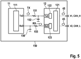
- Fig. 5 illustrates a control unit 150 according to a second embodiment.
- capacitors 152, 156 each with a predetermined capacitance are provided here.
- the resistor 151 and the capacitor 152 form an RC element in the signal line between the terminals TxD.
- the resistor 155 and the capacitor 156 form an RC element in the signal line between the connections RxD.
- the capacitance of the capacitor 152 also interacts with the parasitic capacitance of the line between the TxD connections.
- the capacitance of capacitor 156 interacts with the parasitic capacitance of the line between the RxD terminals.
- the time delay of the transmission signal TX and / or the reception signal RX can be further optimized in comparison to the control unit 15 for improving the bit timing.
- At least one of the capacitors 152, 156 is preferably adjustable with regard to its capacitance value.
- the setting can be carried out in particular by connecting or disconnecting the desired capacitor 152, 156 with a switch.
- the bus status can be, for example, that the minimum value or the maximum value according to, for example, table 13 of the above-mentioned specification ISO11898-2: 2016 for at least one of the above-mentioned parameters is not complied with. If, for example, it is determined as the bus state that the parameter Tbit_bus is too small, then the resistor 151 and / or the capacitor 152 is increased. If, on the other hand, it is determined as the bus state that the parameter Tbit_bus is too large, then the resistor 151 and / or the capacitor 152 is reduced.
- control units 15, 150 The method described with the control units 15, 150 is based on a signal according to FIG Fig. 4 in which a single recessive bit 455 is preceded and followed by a dominant phase or a dominant bus state 4502. It is of course also possible for the dominant and / or the recessive phase to include one or more bits.
- the above-described bus system 1 according to the first to third exemplary embodiments is described using a bus system based on the CAN protocol.
- the bus system 1 according to the first to third exemplary embodiments can, however, also be a different type of communication network. It is advantageous, but not a mandatory prerequisite, that the bus system 1 has an exclusive, collision-free one at least for certain periods of time Access of a subscriber station 10, 20, 30 to the bus line 40 or a common channel of the bus line 40 is guaranteed.
- the bus system 1 is in particular a CAN network or a CAN FD network or a FlexRay network.
- the number and arrangement of the subscriber stations 10, 20, 30 in the bus systems 1 according to the first to third exemplary embodiments is arbitrary. In particular, only subscriber stations 10 or subscriber stations 30 can also be present in the bus systems 1 of the first to third exemplary embodiments.
- the data transmission can take place within the CAN frame of the messages 45, 46, 47 analogous to data transmission protocols such as Ethernet, etc.
Description
Die vorliegende Erfindung betrifft eine Teilnehmerstation für ein Bussystem und ein Verfahren zur Verbesserung der Einhaltung der Bit-Timing-Anforderung in einem Bussystem, um auch bei einer möglichen Asymmetrie von empfangenen Bits bei hohen Datenraten eine gute Empfangsqualität zu erzielen.The present invention relates to a subscriber station for a bus system and a method for improving compliance with the bit timing requirement in a bus system in order to achieve good reception quality even with a possible asymmetry of received bits at high data rates.
Zwischen Sensoren und Steuergeräten findet in vielen Bereichen das CAN-Bussystem Anwendung. Beim CAN-Bussystem werden Nachrichten zwischen den Teilnehmern des Bussystems mittels des CAN-Protokolls übertragen, wie es in der CAN-Spezifikation in der ISO11898 beschrieben ist.
Ein klassischer CAN-Rahmen ist aufgeteilt in Arbitrations- und Datenfeld. Mit dem Arbitrationsfeld wird mit Hilfe einer bitweisen Arbitrierung bestimmt, welcher der Teilnehmer des Bussystems einen exklusiven Zugriff auf ein Kommunikationsmedium zwischen den Teilnehmern des Bussystems hat. Hierbei können, wie bereits in der
Bei dem CAN-Protokoll ist die Bitrate in Arbitrierungs- und Datenfeld gleich, so dass gilt Bitrate_arb = Bitrate_data. Die maximale Bitrate beträgt 1 Mbps (Mega Bit pro Sekunde), das heißt die Bitzeit beträgt 1µs.With the CAN protocol, the bit rate in the arbitration and data fields is the same, so that Bitrate_arb = Bitrate_data. The maximum bit rate is 1 Mbps (mega bits per second), that means the bit time is 1µs.
Das CAN-Protokoll wurde unter dem Namen CAN-FD weiterentwickelt, gemäß welchem Nachrichten entsprechend Spezifikation "CAN with Flexible Data-Rate, Specification Version 1.0" (Quelle http://www.semiconductors.bosch.de) übertragen werden. Mit CAN-FD ist eine Erhöhung der Datenrate für Systeme möglich, bei welchen die Datenrate bisher durch die Buslänge der Systeme begrenzt war.The CAN protocol was further developed under the name CAN-FD, according to which messages are transmitted according to the specification "CAN with Flexible Data-Rate, Specification Version 1.0" (source http://www.semiconductors.bosch.de). With CAN-FD it is possible to increase the data rate for systems in which the data rate was previously limited by the bus length of the systems.
Bei CAN-FD wird im Vergleich zum klassischen CAN am Ende der Arbitrationsphase die Bitrate für die folgende Datenphase auf beispielsweise 2 Mbps, 5 Mbps erhöht. Daher gilt Bitrate_arb < Bitrate_data.In the case of CAN-FD, the bit rate for the following data phase is increased to, for example, 2 Mbps, 5 Mbps at the end of the arbitration phase compared to the classic CAN. Therefore Bitrate_arb <Bitrate_data applies.
In der Datenphase mit höherer Bitrate, wie beispielsweise 2 oder 5 Mbit/s, ist es nun sehr wichtig, dass die Zustandswechsel vom dominanten Zustand zum rezessiven Zustand und vom rezessiven Zustand zum dominanten Zustand bezüglich Ihrer Dauer möglichst gleich sind. Das gilt für den Sendepfad über den Anschluss TxD für ein Sendesignal hin zum Bus (VDIFF=CAN_H-CAN_L) und auch vom Bus (VDIFF) hin zum Anschluss RxD für ein Empfangssignal. Damit kann eine gewisse Mindest-Bitzeit eines einzelnen Bits des CAN-Rahmens garantiert werden. Bei starker Ungleichheit dieser Zeiten unterschreiten Bitzeiten einzelner Bits einen in der Physical Layer Spezifikation ISO11898-2:2016 festgelegten Mindestwert und könnten vom CAN-Protocol-Controller oder einer Kommunikationssteuereinrichtung einer Teilnehmerstation des Bussystems nicht mehr erkannt werden.In the data phase with a higher bit rate, such as 2 or 5 Mbit / s, it is now very important that the changes in status from the dominant state to the recessive state and from the recessive state to the dominant state are as long as possible. This applies to the send path via the TxD connection for a send signal to the bus (VDIFF = CAN_H-CAN_L) and also from the bus (VDIFF) to the RxD connection for a receive signal. A certain minimum bit time of an individual bit of the CAN frame can thus be guaranteed. If these times are very unequal, the bit times of individual bits fall below a minimum value specified in the physical layer specification ISO11898-2: 2016 and could no longer be recognized by the CAN protocol controller or a communication control device of a subscriber station of the bus system.
Dies führt zu Störungen in der Kommunikation im Bussystem. Je nach erfolgter Störung kann dies sicherheitsrelevante Folgen für einen Benutzer des Bussystems oder der im Bussystem verbundenen Sensoren und Steuergeräte haben. Um dies zu vermeiden, sind die Anwender des Bussystems gezwungen, das Bussystem in sehr engen Grenzen oder sehr wenig Freiheitsgraden bei der Auslegung der Bustopologie und Bitrate zu dimensionieren.This leads to disturbances in the communication in the bus system. Depending on the malfunction that has occurred, this can have safety-related consequences for a user of the bus system or the sensors and control devices connected in the bus system. In order to avoid this, the users of the bus system are forced to dimension the bus system within very narrow limits or with very few degrees of freedom when designing the bus topology and bit rate.
Die Offenlegungsschrift
Die Offenlegungsschrift
Daher ist es Aufgabe der vorliegenden Erfindung, eine Teilnehmerstation für ein Bussystem und ein Verfahren zur Verbesserung der Einhaltung der Bit-Timing-Anforderung in einem Bussystem bereitzustellen, welche die zuvor genannten Probleme lösen. Insbesondere sollen eine Teilnehmerstation für ein Bussystem und ein Verfahren zur Verbesserung der Einhaltung der Bit-Timing-Anforderung in einem Bussystem bereitgestellt werden, bei welchen die Einhaltung der Bit-Timing-Anforderungen einfach, wirksam und kostengünstig erfüllt werden kann, so dass keine fehlerhaften Übertragungen auftreten.It is therefore the object of the present invention to provide a subscriber station for a bus system and a method for improving compliance with the bit timing requirement in a bus system which solve the aforementioned problems. In particular, a subscriber station for a bus system and a method for improving compliance with the bit timing requirement in a bus system are to be provided in which compliance with the bit timing requirements can be met simply, effectively and inexpensively, so that no faulty transmissions appear.
Die Aufgabe wird durch eine Teilnehmerstation für ein Bussystem nach Anspruch 1 gelöst.The object is achieved by a subscriber station for a bus system according to claim 1.
Mit der Teilnehmerstation ist auf sehr einfache und damit kostengünstige Weise die Einhaltung der Bit-Timing-Anforderung des Bussystems sicherer als bisher möglich. Dadurch werden fehlerhafte Übertragungen zwischen Teilnehmerstationen des Bussystems verhindert bzw. Systemanwendungen mit CAN-FD ermöglicht. Die verbesserte Einhaltung der Bit-Timing-Anforderung schafft Spielraum für die Dimensionierung der Bustopologie.With the subscriber station, compliance with the bit timing requirement of the bus system is more reliable than before in a very simple and therefore inexpensive way. This prevents incorrect transmissions between subscriber stations of the bus system and enables system applications with CAN-FD. The improved compliance with the bit timing requirement creates scope for dimensioning the bus topology.
Die Einhaltung der Bit-Timing-Anforderung des Bussystems wird durch eine gezielte Beschaltung mit mindestens einem elektrischen Widerstand zwischen der Kommunikationssteuereinrichtung und der Sende-Empfangseinrichtung einer elektronischen Steuereinheit der Teilnehmerstation erreicht. Dadurch wird ermöglicht, eine elektronische Steuereinheit (ECU) der Teilnehmerstation von CAN auf CAN-FD zu migrieren, ohne die Sende-/Empfangseinrichtung oder den Transceiver austauschen zu müssen. Aufgrund dessen kann die Migration von CAN auf CAN-FD ohne Neuentwicklung der Sende-/Empfangseinrichtung oder des Transceivers erfolgen. Dadurch ergibt sich ein deutlicher Kostenvorteil.Compliance with the bit timing requirement of the bus system is achieved through targeted wiring with at least one electrical resistor between the communication control device and the transceiver of an electronic control unit of the subscriber station. This makes it possible to migrate an electronic control unit (ECU) of the subscriber station from CAN to CAN-FD without having to exchange the transmitting / receiving device or the transceiver. Because of this, the migration from CAN to CAN-FD can take place without redevelopment of the transmitter / receiver device or the transceiver. This results in a clear cost advantage.
Die zuvor beschriebene Ausgestaltung der Teilnehmerstation ist auch bei bereits bestehenden Teilnehmerstationen einfach nachrüstbar. Dies ist besonders für Teilnehmerstationen von Vorteil, die in Bezug auf ein CAN-FD-Bit-Timing im grenzlagigen Bereich betrieben werden müssten. Mit der zuvor beschriebenen Ausgestaltung der Teilnehmerstation kann ein größerer Sicherheitsabstand für die benötigte Mindest-Bitzeit eines einzelnen Bits des CAN-Rahmens erreicht werden. Dadurch hat der Planer oder Konstrukteur des Bussystems, wie beispielsweise ein Fahrzeughersteller bzw. Anwender, höhere Freiheitsgrade bei der Auslegung der Bustopologie und Bitrate.The configuration of the subscriber station described above can also be easily retrofitted to existing subscriber stations. This is particularly advantageous for subscriber stations that would have to be operated in the borderline area with regard to CAN FD bit timing. With the configuration of the subscriber station described above, a greater safety margin can be achieved for the required minimum bit time of an individual bit of the CAN frame. This gives the planner or designer of the bus system, such as a vehicle manufacturer or user, greater degrees of freedom when designing the bus topology and bit rate.
Vorteilhafte weitere Ausgestaltungen der Teilnehmerstation sind in den abhängigen Ansprüchen beschrieben.Advantageous further refinements of the subscriber station are described in the dependent claims.
Möglicherweise hat die Verzögerungseinheit mindestens einen Widerstand, der mit einer Kapazität ein RC-Glied bildet, das zwischen die Kommunikationssteuereinrichtung und die Sende-/Empfangseinrichtung geschaltet ist, und eine Einheit, die ausgestaltet ist, eine Empfangsschwelle für ein empfangenes Signal für eine ansteigende Flanke des Signals um einen ersten vorbestimmten Wert zeitlich zu verzögern und von einem bisherigen Spannungspegel auf einen niedrigeren Spannungspegel herabzusetzen und für eine fallende Flanke des Signals um einen zweiten vorbestimmten Wert zeitlich zu verzögern und von einem bisherigen Spannungspegel auf einen niedrigeren Spannungspegel herabzusetzen. Hierbei kann die Kapazität eine parasitäre Kapazität der Signalleitung zwischen der Kommunikationssteuereinrichtung und der Sende-/Empfangseinrichtung sein oder zudem eine Kapazität eines Kondensators aufweisen, der mit dem Widerstand als RC-Glied verschaltet ist.The delay unit may have at least one resistor that forms an RC element with a capacitance that is connected between the communication control device and the transceiver, and a unit that is designed to provide a reception threshold for a received signal for a rising edge of the To delay the signal by a first predetermined value and to reduce it from a previous voltage level to a lower voltage level and to delay it by a second predetermined value for a falling edge of the signal and to reduce it from a previous voltage level to a lower voltage level. Here, the capacitance can be a parasitic capacitance of the signal line between the communication control device and the transmitting / receiving device or also have the capacitance of a capacitor that is connected to the resistor as an RC element.
Es ist auch denkbar, dass der mindestens eine Widerstand zwischen einen Anschluss der Kommunikationssteuereinrichtung, der für ein von der Kommunikationssteuereinrichtung zu sendendes Sendesignal vorgesehen ist, und einen Anschluss der Sende-/Empfangseinrichtung geschaltet ist, der für das von der Kommunikationssteuereinrichtung gesendete Sendesignal vorgesehen ist. In diesem Fall kann der Kondensator an seinem einen Anschluss mit dem mindestens einen Widerstand und dem Anschluss der Sende-/Empfangseinrichtung für ein von der Kommunikationssteuereinrichtung gesendetes Sendesignal verbunden und an seinem anderen Anschluss mit Masse verbunden.It is also conceivable that the at least one resistor is connected between a connection of the communication control device, which is provided for a transmission signal to be transmitted by the communication control device, and a connection of the transmission / reception device, which is provided for the transmission signal transmitted by the communication control device. In this case, the capacitor can be connected at its one connection to the at least one resistor and the connection of the transmitting / receiving device for a transmission signal sent by the communication control device and connected to ground at its other connection.
Es ist außerdem denkbar, dass der mindestens eine Widerstand zwischen einen Anschluss der Sende-/Empfangseinrichtung, der für ein von der Sende-/Empfangseinrichtung vom Bus empfangenes Empfangssignal vorgesehen ist, und einen Anschluss der Kommunikationssteuereinrichtung geschaltet ist, der für das von der Sende-/Empfangseinrichtung vom Bus empfangene Empfangssignal vorgesehen ist. Hierbei kann der Kondensator an seinem einen Anschluss mit dem mindestens einen Widerstand und dem Anschluss (RxD) der Kommunikationssteuereinrichtung für ein von der Sende-/Empfangseinrichtung empfangenes Empfangssignal verbunden sein und an seinem anderen Anschluss mit Masse verbunden sein.It is also conceivable that the at least one resistor is connected between a connection of the transmitting / receiving device, which is provided for a received signal received by the transmitting / receiving device from the bus, and a connection of the communication control device, which is intended for the transmission by the transmitting / receiving device. / Receiving device received from the bus is provided. Here, the capacitor can be connected at its one connection to the at least one resistor and the connection (RxD) of the communication control device for a received signal received by the transmitting / receiving device and connected to ground at its other connection.
Vorteilhaft ist auch, wenn die Verzögerungseinheit ausgestaltet ist, die Verzögerung abhängig vom Buszustand einzubringen. Zusätzlich oder alternativ kann die Sende-/Empfangseinrichtung eine Einheit aufweisen, die ausgestaltet ist, das auf den Bus zu sendende Signal abhängig vom Buszustand zeitlich zu verzögern. Zusätzlich oder alternativ kann die Kommunikationssteuereinrichtung eine Einheit aufweisen, die ausgestaltet ist, das zu sendende Sendesignal oder das von der Sende-/Empfangseinrichtung vom Bus empfangene Empfangssignal abhängig vom Buszustand zeitlich zu verzögern. Zusätzlich oder alternativ kann die Sende-/Empfangseinrichtung eine Einheit aufweisen, die ausgestaltet ist, Buspegel eines TxD-Treibers herabzusetzen und/oder eines RxD-Treibers herabzusetzen. In allen diesen Ausführungsvarianten kann die Einhaltung der Bit-Timing-Anforderung des Bussystems sehr flexibel an die jeweiligen vorhandenen Gegebenheiten angepasst werden.It is also advantageous if the delay unit is designed to introduce the delay as a function of the bus state. Additionally or alternatively, the transmitting / receiving device can have a unit which is designed to delay the signal to be transmitted on the bus in time as a function of the bus state. Additionally or alternatively, the communication control device can have a unit which is designed to delay the transmission signal to be transmitted or the reception signal received from the bus by the transmission / reception device as a function of the bus status. Additionally or alternatively, the transmitting / receiving device can have a unit which is designed to reduce the bus level of a TxD driver and / or an RxD driver to belittle. In all of these design variants, compliance with the bit timing requirement of the bus system can be adapted very flexibly to the respective existing conditions.
Die zuvor beschriebene Teilnehmerstation kann Teil eines Bussystems sein, das einen Bus und mindestens zwei Teilnehmerstationen aufweist, welche über den Bus derart miteinander verbunden sind, dass sie miteinander kommunizieren können, wobei mindestens eine der mindestens zwei Teilnehmerstationen eine zuvor beschriebene Teilnehmerstation ist.The subscriber station described above can be part of a bus system that has a bus and at least two subscriber stations which are connected to one another via the bus in such a way that they can communicate with one another, at least one of the at least two subscriber stations being a previously described subscriber station.
Die zuvor genannte Aufgabe wird zudem durch ein Verfahren zur Verbesserung der Einhaltung der Bit-Timing-Anforderung in einem Bussystem nach Anspruch 10 gelöst.The aforementioned object is also achieved by a method for improving compliance with the bit timing requirement in a bus system according to
Das Verfahren bietet dieselben Vorteile, wie sie zuvor in Bezug auf die Teilnehmerstation genannt sind.The method offers the same advantages as mentioned above with regard to the subscriber station.
Weitere mögliche Implementierungen der Erfindung umfassen auch nicht explizit genannte Kombinationen von zuvor oder im Folgenden bezüglich der Ausführungsbeispiele beschriebenen Merkmale oder Ausführungsformen. Dabei wird der Fachmann auch Einzelaspekte als Verbesserungen oder Ergänzungen zu der jeweiligen Grundform der Erfindung hinzufügen. Der Schutzbereich der Erfindung ist durch den Wortlaut der Ansprüche festgelegt.Further possible implementations of the invention also include combinations, not explicitly mentioned, of features or embodiments described above or below with regard to the exemplary embodiments. The person skilled in the art will also add individual aspects as improvements or additions to the respective basic form of the invention. The scope of the invention is defined by the wording of the claims.
Nachfolgend ist die Erfindung unter Bezugnahme auf die beiliegende Zeichnung und anhand von Ausführungsbeispielen näher beschrieben. Es zeigen:
-
Fig. 1 ein vereinfachtes Blockschaltbild eines Bussystems gemäß einem ersten Ausführungsbeispiel; -
Fig. 2 ein Schaubild zur Veranschaulichung des Aufbaus einer Nachricht, die von einer Teilnehmerstation des Bussystems gemäß dem ersten Ausführungsbeispiel gesendet wird; -
Fig. 3 ein vereinfachtes Schaltbild einer elektronischen Steuereinheit als Steuergerät für die Teilnehmerstation des Bussystems gemäß dem ersten Ausführungsbeispiel; -
Fig. 4 einen Spannungsverlauf eines Empfangssignals über der Zeit, wie es an einer Kommunikationssteuereinrichtung der Teilnehmerstation des Bussystems gemäß dem ersten Ausführungsbeispiel empfangen wird, im Vergleich zu einem Empfangssignal über der Zeit, wie es an einer Kommunikationssteuereinrichtung einer herkömmlichen Teilnehmerstation für das Bussystem empfangen wird; und -
Fig. 5 ein vereinfachtes Schaltbild einer elektronischen Steuereinheit für eine Teilnehmerstation eines Bussystems gemäß einem zweiten Ausführungsbeispiel.
-
Fig. 1 a simplified block diagram of a bus system according to a first embodiment; -
Fig. 2 a diagram to illustrate the structure of a message that is sent by a subscriber station of the bus system according to the first embodiment; -
Fig. 3 a simplified circuit diagram of an electronic control unit as a control device for the subscriber station of the bus system according to the first embodiment; -
Fig. 4 a voltage curve of a received signal over time, as it is received at a communication control device of the subscriber station of the bus system according to the first embodiment, compared to a received signal over time, as it is received at a communication control device of a conventional subscriber station for the bus system; and -
Fig. 5 a simplified circuit diagram of an electronic control unit for a subscriber station of a bus system according to a second embodiment.
In den Figuren sind gleiche oder funktionsgleiche Elemente, sofern nichts anderes angegeben ist, mit denselben Bezugszeichen versehen.In the figures, elements that are the same or have the same function are provided with the same reference symbols unless otherwise specified.
In
Wie in
Die Kommunikationssteuereinrichtung 11 dient zur Steuerung einer Kommunikation der jeweiligen Teilnehmerstation 10, 20, 30 über den Bus 40 mit einer anderen Teilnehmerstation der an den Bus 40 angeschlossenen Teilnehmerstationen 10, 20, 30. Die Kommunikationssteuereinrichtung 11 kann wie ein herkömmlicher CAN-Controller und/oder CAN-FD-Controller ausgeführt sein.The
Die Sende-/Empfangseinrichtung 13 der Teilnehmerstation 20 dient zum Senden der Nachrichten 46 in Form eines Sendesignals TX an eine andere Teilnehmerstation des Bussystems 1 und zum Empfangen der Nachrichten 45, 47 der anderen Teilnehmerstationen des Bussystems 1 in Form eines Empfangssignals RX. Die Sende-/Empfangseinrichtung 13 kann wie ein herkömmlicher CAN-Transceiver ausgeführt sein.The transmitting / receiving
Gemäß
In
Somit ist die TxD-Signalleitung für das Sendesignal TX an TxD-Anschlüsse der Kommunikationssteuereinrichtung 11 und der Sende-/Empfangseinrichtung 12 angeschlossen. Zudem ist die RxD-Signalleitung für das Empfangssignal RX an RxD-Anschlüsse der Kommunikationssteuereinrichtung 11 und der Sende-/Empfangseinrichtung 12 angeschlossen. In die TxD-Signalleitung ist mindestens ein Widerstand 151 in Reihe geschaltet. Zudem ist in die RxD-Signalleitung mindestens ein Widerstand 155 in Reihe geschaltet.The TxD signal line for the transmission signal TX is thus connected to TxD connections of the
Im Betrieb des Steuergeräts 15 sendet die Kommunikationssteuereinrichtung 11 oder Protocol Controller über die TxD-Signalleitung an die Sende-/Empfangseinrichtung 12 je nach Bedarf Daten in Form des Sendesignals TX für beispielsweise eine Nachricht 45. Die Sende-/Empfangseinrichtung 12 setzt das Sendesignal TX als Nachricht 45 auf den Busleitungen 41, 42 oder CAN_H und CAN_L um. Außerdem wird beispielsweise eine Nachricht 47, die von der Sende-/Empfangseinrichtung 12 über die Busleitungen 41, 42 oder CAN_H und CAN_L empfangen wurde, mittels der Sende-/Empfangseinrichtung 12 als Daten in Form des Empfangssignals RX umgesetzt und über die RxD-Signalleitung an die Kommunikationssteuereinrichtung 11 weitergeleitet.When the
Durch den zusätzlich in die TxD-Signalleitung eingebauten mindestens einen Widerstand 151 werden die CAN-FD-Bit-Timings des Signals auf der TxD-Signalleitung positiv beeinflusst. Durch den zusätzlich in die RxD-Signalleitung eingebauten mindestens einen Widerstand 155 werden die CAN-FD-Bit-Timings des Signals auf der RxD-Signalleitung positiv beeinflusst. Dies ist in
In
Bei dem Beispiel von
Als Folge davon erreicht das Bit 455 aufgrund des Widerstands 155 nach einem Zustandswechsel von dem dominanten Buszustand 4502 zu dem rezessiven Buszustand 4501 in
Somit ergibt sich durch die Einbringung der Beschaltung mit dem Widerstand 155 in Zusammenwirken mit einer parasitären Kapazität der Leitung zwischen den RxD-Anschlüssen ein RC-Verhalten auf den Signalleitungen zwischen der Kontrollsteuereinrichtung 11 und der Sende-/Empfangseinrichtung 12. Daraus resultieren weniger steile Flanken für das Bit 455 bei den Zustandswechseln zwischen dem dominanten Buszustand 4502 und dem rezessiven Buszustand 4501, welche einer ansteigenden Flanke des Signals entsprechen. Wie in
Infolgedessen verschiebt die Auswerteeinheit 111 den Empfangspegel am Eingang der Kontrollsteuereinrichtung 11, also am Anschluss RxD der Kontrollsteuereinrichtung 11, für eine ansteigende Flanke des Signals RX von dem Spannungspegel 456A auf den Spannungspegel 455A und für eine fallende Flanke des Signals RX von dem Spannungspegel 456B auf den Spannungspegel 455B. Dies ist beispielsweise durch eine entsprechende Programmierung der Kontrollsteuereinrichtung 11 mit der Auswerteeinheit 111 ausführbar. Außerdem tastet die Kontrollsteuereinrichtung 11 das Bit 455 und somit das Empfangssignal RX nicht mehr mit der herkömmlichen Abtastdauer T1 für ein rezessives Bit 456 ab, sondern mit einer verlängerten Zeitdauer T2. Die Zeitdauer T2 beginnt im Vergleich zu der herkömmlichen Abtastdauer T1 um eine vorbestimmte Zeitdauer TV1 später oder ist um eine Verzögerungszeitdauer TV1 zeitlich verzögert. Außerdem endet die Zeitdauer T2 im Vergleich zu der herkömmlichen Abtastdauer T1 um eine vorbestimmte Zeitdauer TV2 später. Somit ist auch der Endzeitpunkt der Abtastung um eine Verzögerungszeitdauer TV2 zeitlich verzögert. Die Verzögerungszeitdauer TV1 ist kleiner als die Verzögerungszeitdauer TV2.As a result, the
Somit wird ein größerer Sicherheitsabstand für die benötigte Mindest-Bitzeit eines einzelnen Bits 455 des CAN-Rahmens oder CAN-FD-Rahmens einer Nachricht 45 in der Steuereinheit 15 erreicht. Genauer gesagt, ändert sich durch den Widerstand 155 der Parameter delta-rec aus insbesondere den Tabellen 13 und 14 der Spezifikation ISO11898-2:2016. Als Folge davon verändert sich auch tbit_rxd der Spezifikation ISO11898-2:2016.A greater safety margin is thus achieved for the required minimum bit time of an
Dadurch können insbesondere die Vorgaben der Spezifikation ISO11898-2:2016 für eine Bitrate von 2 Mbit/s gemäß Tabelle 13 und für eine Bitrate von 5 Mbit/s gemäß Tabelle 14 besser erfüllt werden als mit einer herkömmlichen Steuereinheit, welche den Widerstand 155 nicht aufweist.As a result, the requirements of the ISO11898-2: 2016 specification for a bit rate of 2 Mbit / s according to Table 13 and for a bit rate of 5 Mbit / s according to Table 14 can be met better than with a conventional control unit that does not have
Zusätzlich oder alternativ ist der Widerstand 151 in der TxD-Signalleitung vorhanden. In diesem Fall verschiebt die Empfangspegelanpasseinheit 121 den Empfangspegel am Eingang der Sende-/Empfangseinrichtung 12, also am Anschluss TxD der Sende-/Empfangseinrichtung 12 von dem Spannungspegel 456A auf den Spannungspegel 455A und von dem Spannungspegel 456B auf den Spannungspegel 455B. Auch dies ist beispielsweise durch eine entsprechende Programmierung der Sende-/Empfangseinrichtung 12 mit der Empfangspegelanpasseinheit 121 ausführbar. In diesem Fall ändert sich durch den Widerstand 151 der Parameter t-bit-bus aus insbesondere den Tabellen 13 und 14 der Spezifikation ISO11898-2:2016. Als Folge davon verändert sich auch der Parameter tbit_rxd der Spezifikation ISO11898-2:2016.Additionally or alternatively, the
Mit dem zuvor beschriebenen Verfahren zur Verbesserung der Einhaltung der Bit-Timing-Anforderung in dem Bussystem 1 ist es möglich, zusätzlich oder alternativ in dem Sendesignal TX einen größeren Sicherheitsabstand für die benötigte Mindest-Bitzeit eines einzelnen Bits 455 des CAN-Rahmens oder CAN-FD-Rahmens einer Nachricht 45 in der Steuereinheit 15 zu erreichen. Dadurch können die Vorgaben aus Tabelle 13 und 14 der CAN-Spezifikation ISO11898-2:2016 besser erfüllt werden als mit der herkömmlichen Steuereinheit, welche den Widerstand 151 nicht aufweist.With the method described above to improve compliance with the bit timing requirement in bus system 1, it is possible, in addition or as an alternative, to use a larger safety margin for the required minimum bit time of an
Die Widerstände 151, 155 sind derart ausgelegt, dass die bewirkte zeitliche Verzögerung der einzelnen Bits 455 des CAN-Rahmens oder CAN-FD-Rahmens einer Nachricht 45 nicht so groß wird, dass die Anforderung der Propagation Delay Time gemäß der CAN-Spezifikation ISO11898-2:2016 nicht erfüllt werden kann. Die Propagation Delay Time gemäß der CAN-Spezifikation ISO11898-2:2016 beträgt maximal 255ns von dem TxD-Anschluss der Kommunikationssteuereinrichtung 11 auf den Bus 40 und von dort zurück über den RxD-Anschluss zu der Kommunikationssteuereinrichtung 11.The
Bei einer Modifikation der Schaltung von
Die Einstellung des Widerstandswerts kann insbesondere mit der Auswerteeinheit 111 und/oder der Empfangspegeleinstelleinheit 121 ausgeführt werden. Dadurch kann in der Signalleitung, die durch die Einstellung des zugehörigen Widerstands 151, 155 betroffen ist, die zuvor beschriebene Verzögerung der Zustandswechsel oder ansteigenden oder fallenden Flanken des Signals abhängig vom jeweiligen Buszustand eingestellt werden.The setting of the resistance value can in particular be carried out with the
Zusätzlich oder alternativ ist die Sende-/Empfangseinrichtung 12, insbesondere die Empfangspegelanpasseinheit 121, bei einer weiteren Modifikation der Schaltung von
Bei noch einer weiteren Modifikation der Schaltung von
Bei noch einer weiteren Modifikation der Schaltung von
Mit Hilfe der genannten Modifikationen ist ein noch größerer Sicherheitsabstand für die benötigte Mindest-Bitzeit eines einzelnen Bits 455 des CAN-Rahmens oder CAN-FD-Rahmens einer Nachricht 45 in der Steuereinheit 15 erreichbar.With the aid of the modifications mentioned, an even greater safety margin for the required minimum bit time of an
Auf diese Weise kann die zeitliche Verzögerung des Sendesignals TX und/oder des Empfangssignals RX im Vergleich zu der Steuereinheit 15 für die Verbesserung des Bit-Timings weiter optimiert werden.In this way, the time delay of the transmission signal TX and / or the reception signal RX can be further optimized in comparison to the
Vorzugsweise ist mindestens einer der Kondensatoren 152, 156 in Bezug auf seinen Kapazitätswert einstellbar. Die Einstellung kann insbesondere durch Zu- oder Abschaltung des gewünschten Kondensators 152, 156 mit einem Schalter ausgeführt werden.At least one of the
Auf diese Weise ist es sehr flexibel möglich, die zeitliche Verzögerung des Sendesignals TX und des Empfangssignals RX je nach Bedarf an den jeweiligen Buszustand anzupassen. Der Buszustand kann beispielsweise sein, dass der minimale Wert oder der maximale Wert gemäß beispielsweise der Tabelle 13 der oben genannten Spezifikation ISO11898-2:2016 für mindestens einen der zuvor genannten Parameter nicht eingehalten ist. Wird beispielsweise als Buszustand ermittelt, dass der Parameter Tbit_bus zu klein ist, dann wird der Widerstand 151 und/oder der Kondensator 152 vergrößert. Wird dagegen als Buszustand ermittelt, dass der Parameter Tbit_bus zu groß ist, dann wird der Widerstand 151 und/oder der Kondensator 152 verkleinert. Wird beispielsweise als Buszustand ermittelt, dass der Parameter Tbit_bus in dem zulässigen Wertebereich liegt, aber Tbit_rxd zu klein ist, dann wird der Widerstand 155 und/oder der Kondensator 156 vergrößert. Wird dagegen als Buszustand ermittelt, dass der Parameter Tbit_bus in dem zulässigen Wertebereich liegt, aber Tbit_rxd zu groß ist, dann wird der Widerstand 155 und/oder der Kondensator 156 verkleinertIn this way, it is possible in a very flexible manner to adapt the time delay of the transmission signal TX and the reception signal RX to the respective bus state as required. The bus status can be, for example, that the minimum value or the maximum value according to, for example, table 13 of the above-mentioned specification ISO11898-2: 2016 for at least one of the above-mentioned parameters is not complied with. If, for example, it is determined as the bus state that the parameter Tbit_bus is too small, then the
Dadurch wird noch ein größerer Sicherheitsabstand für die benötigte Mindest-Bitzeit eines einzelnen Bits 455 des CAN-Rahmens oder CAN-FD-Rahmens einer Nachricht 45 in der Steuereinheit 15 erreicht.As a result, an even greater safety margin is achieved for the required minimum bit time of an
Alle zuvor beschriebenen Ausgestaltungen des Bussystems 1 der Teilnehmerstationen 10, 20,30 und des Verfahrens gemäß den Ausführungsbeispielen und deren Modifikationen können einzeln oder in allen möglichen Kombinationen Verwendung finden. Zusätzlich sind insbesondere folgende Modifikationen denkbar.All of the above-described configurations of the bus system 1 of the
Das mit den Steuereinheiten 15, 150 beschriebene Verfahren ist anhand eines Signals gemäß
Das zuvor beschriebene Bussystem 1 gemäß dem ersten bis dritten Ausführungsbeispiel ist anhand eines auf dem CAN-Protokoll basierenden Bussystems beschrieben. Das Bussystem 1 gemäß dem ersten bis dritten Ausführungsbeispiel kann jedoch auch eine andere Art von Kommunikationsnetz sein. Es ist vorteilhaft, jedoch nicht zwangsläufige Voraussetzung, dass bei dem Bussystem 1 zumindest für bestimmte Zeitspannen ein exklusiver, kollisionsfreier Zugriff einer Teilnehmerstation 10, 20, 30 auf die Busleitung 40 oder einen gemeinsamen Kanal der Busleitung 40 gewährleistet ist.The above-described bus system 1 according to the first to third exemplary embodiments is described using a bus system based on the CAN protocol. The bus system 1 according to the first to third exemplary embodiments can, however, also be a different type of communication network. It is advantageous, but not a mandatory prerequisite, that the bus system 1 has an exclusive, collision-free one at least for certain periods of time Access of a
Das Bussystem 1 gemäß dem ersten bis dritten Ausführungsbeispiel ist insbesondere ein CAN-Netzwerk oder ein CAN-FD-Netzwerk oder ein FlexRay-Netzwerk.The bus system 1 according to the first to third exemplary embodiment is in particular a CAN network or a CAN FD network or a FlexRay network.
Die Anzahl und Anordnung der Teilnehmerstationen 10, 20, 30 in den Bussystemen 1 gemäß dem ersten bis dritten Ausführungsbeispiel ist beliebig. Insbesondere können auch nur Teilnehmerstationen 10 oder Teilnehmerstationen 30 in den Bussystemen 1 des ersten bis dritten Ausführungsbeispiels vorhanden sein.The number and arrangement of the
Um eine noch höhere Datenrate zu erzielen, kann innerhalb des CAN-Rahmens der Nachrichten 45, 46, 47 die Datenübertragung analog zu Datenübertragungsprotokollen erfolgen, wie beispielsweise Ethernet, usw.In order to achieve an even higher data rate, the data transmission can take place within the CAN frame of the
Claims (10)
- Subscriber station (10; 30) for a bus system (1), having
a transmission/reception device (12) for transmitting or receiving a message (45; 46; 47) to/from at least one further subscriber station of the bus system (1) via the bus system (1), in which bus system (1), at least intermittently, exclusive collision-free access by a subscriber station (10,20,30) to a bus (40) of the bus system (1) is ensured, and
a communication control device (11) for creating the message (45; 46; 47) to be transmitted by the transmission/reception device (12) or for reading the message (45; 46; 47) received by the transmission/reception device (12) according to a predetermined communication protocol for the bus system (1),
and a delay unit connected between the communication control device (11) and the transmission/reception device (12) in order to delay a transmission signal (TX) transmitted from the communication control device (11) to the transmission/reception device (12) and a received signal (RX) received by the transmission/reception device (12). - Subscriber station (10; 30) according to Claim 1, wherein the delay unit has
at least one resistor (151; 155) forming, with a capacitance, an RC element connected between the communication control device (11) and the transmission/reception device (12), and
a unit (111; 121) configured to delay the timing of a reception threshold for a received signal (TX; RX) for a rising edge of the signal (TX; RX) by a first predetermined value (TV1) and to lower said reception threshold from a previous voltage level (456A) to a lower voltage level (455A) and to delay the timing of said reception threshold for a falling edge of the signal (TX; RX) by a second predetermined value (TV2) and to lower said reception threshold from a previous voltage level (456B) to a lower voltage level (455B). - Subscriber station (10; 30) according to Claim 2, wherein the capacitance is a parasitic capacitance of the signal line between the communication control device (11) and the transmission/reception device (12) or moreover has a capacitance of a capacitor (152; 156) connected up to the resistor (151; 155) as an RC element.
- Subscriber station (10; 30) according to Claim 2 or 3, wherein the at least one resistor (151) is connected between a connection (TxD) of the communication control device (11) that is intended for a transmission signal (TX) to be transmitted by the communication control device (11) and a connection (TxD) of the transmission/reception device (12) that is intended for the transmission signal (TX) transmitted by the communication control device (11).
- Subscriber station (10; 30) according to Claim 3 or 4, wherein the capacitor (152) has its one connection connected to the at least one resistor (151) and the connection (TxD) of the transmission/reception device (12) for a transmission signal (TX) transmitted by the communication control device (11) and has its other connection connected to earth.
- Subscriber station (10; 30) according to one of the preceding claims, wherein the at least one resistor (155) is connected between a connection (RxD) of the transmission/reception device (12) that is intended for a received signal (RX) received by the transmission/reception device (12) from the bus and a connection (RxD) of the communication control device (11) that is intended for the received signal received by the transmission/reception device (12) from the bus.
- Subscriber station (10; 30) according to Claim 6, wherein the capacitor (156) has its one connection connected to the at least one resistor (155) and the connection (RxD) of the communication control device (11) for a received signal (RX) received by the transmission/reception device (12) and has its other connection connected to earth.
- Subscriber station (10; 30) according to one of the preceding claims,
wherein the delay unit is configured to introduce the delay on the basis of the bus state, and/or
wherein the transmission/reception device (12) has a unit (121) configured to delay the timing of the signal (CAN_H, CAN_L) to be transmitted to the bus (40) on the basis of the bus state, and/or
wherein the communication control device (11) has a unit configured to delay the timing of the transmission signal (TX) to be transmitted or of the received signal (RX) received by the transmission/reception device (12) from the bus (40) on the basis of the bus state, and/or wherein the transmission/reception device (12) has a unit (121) configured to lower bus levels of a TxD driver (122) and/or of an RxD driver (123). - Bus system (1), having
a bus (40), and
at least two subscriber stations (10; 20; 30) connected to one another via the bus (4) such that they can communicate with one another,
characterized in that at least one of the at least two subscriber stations (10; 20; 30) is a subscriber station (10; 30) according to one of the preceding claims. - Method for improving the compliance of the bit timing request in a bus system (1), in which, at least intermittently, exclusive collision-free access by a subscriber station (10,20,30) to a bus (40) of the bus system (1) is ensured, wherein the subscriber station has a transmission/reception device (12) for transmitting or receiving a message (45; 46; 47) to/from at least one further subscriber station of the bus system (1) via the bus system (1), and a communication control device (11) for creating the message (45; 46; 47) to be transmitted by the transmission/reception device (12) or for reading the message (45; 46; 47) received by the transmission/reception device (12) according to a predetermined communication protocol for the bus system (1),
and wherein the method has the step of
delaying, by means of a delay unit connected between the communication control device (11) and the transmission/reception device (12), a transmission signal (TX) transmitted from the communication control device (11) to the transmission/reception device (12) and a received signal (RX) received by the transmission/reception device (12).
Applications Claiming Priority (2)
| Application Number | Priority Date | Filing Date | Title |
|---|---|---|---|
| DE102017205785.8A DE102017205785A1 (en) | 2017-04-05 | 2017-04-05 | Subscriber station for a bus system and method for improving the compliance of the bit timing request in a bus system |
| PCT/EP2018/058415 WO2018185064A1 (en) | 2017-04-05 | 2018-04-03 | Subscriber station for a bus system and method for improving the compliance with the bit-timing request in a bus system |
Publications (2)
| Publication Number | Publication Date |
|---|---|
| EP3607703A1 EP3607703A1 (en) | 2020-02-12 |
| EP3607703B1 true EP3607703B1 (en) | 2021-08-11 |
Family
ID=61911579
Family Applications (1)
| Application Number | Title | Priority Date | Filing Date |
|---|---|---|---|
| EP18716199.7A Active EP3607703B1 (en) | 2017-04-05 | 2018-04-03 | Subscriber station for a bus system and method for improving the compliance with the bit-timing request in a bus system |
Country Status (4)
| Country | Link |
|---|---|
| EP (1) | EP3607703B1 (en) |
| CN (1) | CN110679116B (en) |
| DE (1) | DE102017205785A1 (en) |
| WO (1) | WO2018185064A1 (en) |
Families Citing this family (6)
| Publication number | Priority date | Publication date | Assignee | Title |
|---|---|---|---|---|
| DE102018221957A1 (en) | 2018-12-17 | 2020-06-18 | Robert Bosch Gmbh | Device for a subscriber station of a serial bus system and method for communication in a serial bus system |
| US10778481B1 (en) | 2019-03-25 | 2020-09-15 | Delphi Technologies Ip Limited | Adaptable can transceiver and system |
| DE102019208059A1 (en) * | 2019-06-03 | 2020-12-03 | Robert Bosch Gmbh | Device for a subscriber station of a serial bus system and method for communication in a serial bus system |
| DE102020200802A1 (en) * | 2020-01-23 | 2021-07-29 | Robert Bosch Gesellschaft mit beschränkter Haftung | Transmitting / receiving device and communication control device for a subscriber station of a serial bus system and method for communication in a serial bus system |
| DE102020200804A1 (en) * | 2020-01-23 | 2021-07-29 | Robert Bosch Gesellschaft mit beschränkter Haftung | Transmitting / receiving device and communication control device for a subscriber station of a serial bus system and method for communication in a serial bus system |
| DE102021207188A1 (en) * | 2021-07-08 | 2023-01-12 | Robert Bosch Gesellschaft mit beschränkter Haftung | Receiving module and method for receiving differential signals in a serial bus system |
Family Cites Families (8)
| Publication number | Priority date | Publication date | Assignee | Title |
|---|---|---|---|---|
| DE10000305B4 (en) | 2000-01-05 | 2011-08-11 | Robert Bosch GmbH, 70469 | Method and device for exchanging data between at least two subscribers connected to a bus system |
| US7778599B2 (en) * | 2006-05-01 | 2010-08-17 | Intel Corporation | Aggregated channel feedback |
| DE102009026965A1 (en) * | 2009-06-16 | 2010-12-23 | Robert Bosch Gmbh | Media access control method for a bus system and communication device |
| DE102012200997A1 (en) | 2011-08-29 | 2013-02-28 | Robert Bosch Gmbh | Method and device for checking the correct function of a serial data transmission |
| DE102011089587A1 (en) * | 2011-12-22 | 2013-06-27 | Robert Bosch Gmbh | Subscriber station of a bus system and method for transmitting messages between subscriber stations of a bus system |
| DE102014204050A1 (en) * | 2014-03-05 | 2015-09-10 | Robert Bosch Gmbh | Subscriber station for a bus system and method for improving the transmission quality in a bus system |
| DE102014223838A1 (en) * | 2014-11-21 | 2016-05-25 | Robert Bosch Gmbh | Subscriber station for a bus system and a method for controlling a timing of a transmission signal for a bus system |
| EP3319274B1 (en) * | 2016-11-02 | 2019-04-17 | NXP USA, Inc. | Can module and method therefor |
-
2017
- 2017-04-05 DE DE102017205785.8A patent/DE102017205785A1/en active Pending
-
2018
- 2018-04-03 EP EP18716199.7A patent/EP3607703B1/en active Active
- 2018-04-03 WO PCT/EP2018/058415 patent/WO2018185064A1/en unknown
- 2018-04-03 CN CN201880037113.5A patent/CN110679116B/en active Active
Also Published As
| Publication number | Publication date |
|---|---|
| CN110679116B (en) | 2021-11-26 |
| CN110679116A (en) | 2020-01-10 |
| DE102017205785A1 (en) | 2018-10-11 |
| WO2018185064A1 (en) | 2018-10-11 |
| EP3607703A1 (en) | 2020-02-12 |
Similar Documents
| Publication | Publication Date | Title |
|---|---|---|
| EP3607703B1 (en) | Subscriber station for a bus system and method for improving the compliance with the bit-timing request in a bus system | |
| EP3114800B1 (en) | Subscriber station for a bus system and method for improving the quality of transmission in a bus system | |
| EP3114801B1 (en) | Subscriber station for a bus system and method for reducing line-conducted emissions in a bus system | |
| EP2443557B1 (en) | Method for transmitting data between subscriber stations of a bus system | |
| EP2443797B1 (en) | Media access control method for a bus system and communication apparatus | |
| EP2619948B1 (en) | Method and subscriber station for optimized data transmission between subscriber stations in a bus system | |
| EP3028424A1 (en) | Participant station for a bus system and method for improving the error tolerance of a participant station of a bus system | |
| DE102005037263A1 (en) | Method and device for decoding a signal | |
| EP3665872B1 (en) | Oscillation reduction unit for a bus system, and method for reducing an oscillation inclination when transitioning between different bit states | |
| EP3756311B1 (en) | Apparatus and method for a transmitting/receiving device of a bus system | |
| EP3665874B1 (en) | Transceiver for a bus system, and method for reducing an oscillation inclination upon transitioning between different bit states | |
| WO2020035392A1 (en) | Frame screening unit, subscriber station for a serial bus system and method for communication in a serial bus system | |
| DE102019205488A1 (en) | Subscriber station for a serial bus system and method for communication in a serial bus system | |
| EP2534582B1 (en) | Novel circuit and method for communicating via a single line | |
| EP3665869A1 (en) | Transceiver for a bus system, and method for reducing an oscillation inclination upon transitioning between different bit states | |
| DE102021207188A1 (en) | Receiving module and method for receiving differential signals in a serial bus system | |
| WO2023280474A1 (en) | Transmission module and method for transmitting differential signals in a serial bus system | |
| WO2024037766A1 (en) | Interface module for a subscriber station of a serial bus system and method for transmitting a message in a serial bus system | |
| DE102020214649A1 (en) | Subscriber station for a serial bus system and method for communication in a serial bus system | |
| WO2020244986A1 (en) | Subscriber station for a serial bus system and method for communication in a serial bus system | |
| DE102019220022A1 (en) | Transmitting / receiving device for a bus system and method for reducing oscillations of a bus differential voltage in the event of interference |
Legal Events
| Date | Code | Title | Description |
|---|---|---|---|
| STAA | Information on the status of an ep patent application or granted ep patent |
Free format text: STATUS: UNKNOWN |
|
| STAA | Information on the status of an ep patent application or granted ep patent |
Free format text: STATUS: THE INTERNATIONAL PUBLICATION HAS BEEN MADE |
|
| PUAI | Public reference made under article 153(3) epc to a published international application that has entered the european phase |
Free format text: ORIGINAL CODE: 0009012 |
|
| STAA | Information on the status of an ep patent application or granted ep patent |
Free format text: STATUS: REQUEST FOR EXAMINATION WAS MADE |
|
| 17P | Request for examination filed |
Effective date: 20191105 |
|
| AK | Designated contracting states |
Kind code of ref document: A1 Designated state(s): AL AT BE BG CH CY CZ DE DK EE ES FI FR GB GR HR HU IE IS IT LI LT LU LV MC MK MT NL NO PL PT RO RS SE SI SK SM TR |
|
| AX | Request for extension of the european patent |
Extension state: BA ME |
|
| RAP1 | Party data changed (applicant data changed or rights of an application transferred) |
Owner name: ROBERT BOSCH GMBH |
|
| DAV | Request for validation of the european patent (deleted) | ||
| DAX | Request for extension of the european patent (deleted) | ||
| GRAP | Despatch of communication of intention to grant a patent |
Free format text: ORIGINAL CODE: EPIDOSNIGR1 |
|
| STAA | Information on the status of an ep patent application or granted ep patent |
Free format text: STATUS: GRANT OF PATENT IS INTENDED |
|
| INTG | Intention to grant announced |
Effective date: 20210601 |
|
| GRAS | Grant fee paid |
Free format text: ORIGINAL CODE: EPIDOSNIGR3 |
|
| GRAA | (expected) grant |
Free format text: ORIGINAL CODE: 0009210 |
|
| STAA | Information on the status of an ep patent application or granted ep patent |
Free format text: STATUS: THE PATENT HAS BEEN GRANTED |
|
| AK | Designated contracting states |
Kind code of ref document: B1 Designated state(s): AL AT BE BG CH CY CZ DE DK EE ES FI FR GB GR HR HU IE IS IT LI LT LU LV MC MK MT NL NO PL PT RO RS SE SI SK SM TR |
|
| REG | Reference to a national code |
Ref country code: CH Ref legal event code: EP |
|
| REG | Reference to a national code |
Ref country code: DE Ref legal event code: R096 Ref document number: 502018006534 Country of ref document: DE |
|
| REG | Reference to a national code |
Ref country code: NL Ref legal event code: FP |
|
| REG | Reference to a national code |
Ref country code: IE Ref legal event code: FG4D Free format text: LANGUAGE OF EP DOCUMENT: GERMAN Ref country code: AT Ref legal event code: REF Ref document number: 1420522 Country of ref document: AT Kind code of ref document: T Effective date: 20210915 |
|
| REG | Reference to a national code |
Ref country code: LT Ref legal event code: MG9D |
|
| PG25 | Lapsed in a contracting state [announced via postgrant information from national office to epo] |
Ref country code: LT Free format text: LAPSE BECAUSE OF FAILURE TO SUBMIT A TRANSLATION OF THE DESCRIPTION OR TO PAY THE FEE WITHIN THE PRESCRIBED TIME-LIMIT Effective date: 20210811 Ref country code: BG Free format text: LAPSE BECAUSE OF FAILURE TO SUBMIT A TRANSLATION OF THE DESCRIPTION OR TO PAY THE FEE WITHIN THE PRESCRIBED TIME-LIMIT Effective date: 20211111 Ref country code: NO Free format text: LAPSE BECAUSE OF FAILURE TO SUBMIT A TRANSLATION OF THE DESCRIPTION OR TO PAY THE FEE WITHIN THE PRESCRIBED TIME-LIMIT Effective date: 20211111 Ref country code: PT Free format text: LAPSE BECAUSE OF FAILURE TO SUBMIT A TRANSLATION OF THE DESCRIPTION OR TO PAY THE FEE WITHIN THE PRESCRIBED TIME-LIMIT Effective date: 20211213 Ref country code: HR Free format text: LAPSE BECAUSE OF FAILURE TO SUBMIT A TRANSLATION OF THE DESCRIPTION OR TO PAY THE FEE WITHIN THE PRESCRIBED TIME-LIMIT Effective date: 20210811 Ref country code: ES Free format text: LAPSE BECAUSE OF FAILURE TO SUBMIT A TRANSLATION OF THE DESCRIPTION OR TO PAY THE FEE WITHIN THE PRESCRIBED TIME-LIMIT Effective date: 20210811 Ref country code: FI Free format text: LAPSE BECAUSE OF FAILURE TO SUBMIT A TRANSLATION OF THE DESCRIPTION OR TO PAY THE FEE WITHIN THE PRESCRIBED TIME-LIMIT Effective date: 20210811 Ref country code: SE Free format text: LAPSE BECAUSE OF FAILURE TO SUBMIT A TRANSLATION OF THE DESCRIPTION OR TO PAY THE FEE WITHIN THE PRESCRIBED TIME-LIMIT Effective date: 20210811 Ref country code: RS Free format text: LAPSE BECAUSE OF FAILURE TO SUBMIT A TRANSLATION OF THE DESCRIPTION OR TO PAY THE FEE WITHIN THE PRESCRIBED TIME-LIMIT Effective date: 20210811 |
|
| PG25 | Lapsed in a contracting state [announced via postgrant information from national office to epo] |
Ref country code: PL Free format text: LAPSE BECAUSE OF FAILURE TO SUBMIT A TRANSLATION OF THE DESCRIPTION OR TO PAY THE FEE WITHIN THE PRESCRIBED TIME-LIMIT Effective date: 20210811 Ref country code: LV Free format text: LAPSE BECAUSE OF FAILURE TO SUBMIT A TRANSLATION OF THE DESCRIPTION OR TO PAY THE FEE WITHIN THE PRESCRIBED TIME-LIMIT Effective date: 20210811 Ref country code: GR Free format text: LAPSE BECAUSE OF FAILURE TO SUBMIT A TRANSLATION OF THE DESCRIPTION OR TO PAY THE FEE WITHIN THE PRESCRIBED TIME-LIMIT Effective date: 20211112 |
|
| PG25 | Lapsed in a contracting state [announced via postgrant information from national office to epo] |
Ref country code: DK Free format text: LAPSE BECAUSE OF FAILURE TO SUBMIT A TRANSLATION OF THE DESCRIPTION OR TO PAY THE FEE WITHIN THE PRESCRIBED TIME-LIMIT Effective date: 20210811 |
|
| REG | Reference to a national code |
Ref country code: DE Ref legal event code: R097 Ref document number: 502018006534 Country of ref document: DE |
|
| PG25 | Lapsed in a contracting state [announced via postgrant information from national office to epo] |
Ref country code: SM Free format text: LAPSE BECAUSE OF FAILURE TO SUBMIT A TRANSLATION OF THE DESCRIPTION OR TO PAY THE FEE WITHIN THE PRESCRIBED TIME-LIMIT Effective date: 20210811 Ref country code: SK Free format text: LAPSE BECAUSE OF FAILURE TO SUBMIT A TRANSLATION OF THE DESCRIPTION OR TO PAY THE FEE WITHIN THE PRESCRIBED TIME-LIMIT Effective date: 20210811 Ref country code: RO Free format text: LAPSE BECAUSE OF FAILURE TO SUBMIT A TRANSLATION OF THE DESCRIPTION OR TO PAY THE FEE WITHIN THE PRESCRIBED TIME-LIMIT Effective date: 20210811 Ref country code: EE Free format text: LAPSE BECAUSE OF FAILURE TO SUBMIT A TRANSLATION OF THE DESCRIPTION OR TO PAY THE FEE WITHIN THE PRESCRIBED TIME-LIMIT Effective date: 20210811 Ref country code: CZ Free format text: LAPSE BECAUSE OF FAILURE TO SUBMIT A TRANSLATION OF THE DESCRIPTION OR TO PAY THE FEE WITHIN THE PRESCRIBED TIME-LIMIT Effective date: 20210811 Ref country code: AL Free format text: LAPSE BECAUSE OF FAILURE TO SUBMIT A TRANSLATION OF THE DESCRIPTION OR TO PAY THE FEE WITHIN THE PRESCRIBED TIME-LIMIT Effective date: 20210811 |
|
| PLBE | No opposition filed within time limit |
Free format text: ORIGINAL CODE: 0009261 |
|
| STAA | Information on the status of an ep patent application or granted ep patent |
Free format text: STATUS: NO OPPOSITION FILED WITHIN TIME LIMIT |
|
| 26N | No opposition filed |
Effective date: 20220512 |
|
| PG25 | Lapsed in a contracting state [announced via postgrant information from national office to epo] |
Ref country code: SI Free format text: LAPSE BECAUSE OF FAILURE TO SUBMIT A TRANSLATION OF THE DESCRIPTION OR TO PAY THE FEE WITHIN THE PRESCRIBED TIME-LIMIT Effective date: 20210811 |
|
| REG | Reference to a national code |
Ref country code: CH Ref legal event code: PL |
|
| GBPC | Gb: european patent ceased through non-payment of renewal fee |
Effective date: 20220403 |
|
| REG | Reference to a national code |
Ref country code: BE Ref legal event code: MM Effective date: 20220430 |
|
| PG25 | Lapsed in a contracting state [announced via postgrant information from national office to epo] |
Ref country code: MC Free format text: LAPSE BECAUSE OF FAILURE TO SUBMIT A TRANSLATION OF THE DESCRIPTION OR TO PAY THE FEE WITHIN THE PRESCRIBED TIME-LIMIT Effective date: 20210811 Ref country code: LU Free format text: LAPSE BECAUSE OF NON-PAYMENT OF DUE FEES Effective date: 20220403 Ref country code: LI Free format text: LAPSE BECAUSE OF NON-PAYMENT OF DUE FEES Effective date: 20220430 Ref country code: GB Free format text: LAPSE BECAUSE OF NON-PAYMENT OF DUE FEES Effective date: 20220403 Ref country code: CH Free format text: LAPSE BECAUSE OF NON-PAYMENT OF DUE FEES Effective date: 20220430 |
|
| PG25 | Lapsed in a contracting state [announced via postgrant information from national office to epo] |
Ref country code: BE Free format text: LAPSE BECAUSE OF NON-PAYMENT OF DUE FEES Effective date: 20220430 |
|
| PG25 | Lapsed in a contracting state [announced via postgrant information from national office to epo] |
Ref country code: IE Free format text: LAPSE BECAUSE OF NON-PAYMENT OF DUE FEES Effective date: 20220403 |
|
| PGFP | Annual fee paid to national office [announced via postgrant information from national office to epo] |
Ref country code: NL Payment date: 20230417 Year of fee payment: 6 |
|
| PGFP | Annual fee paid to national office [announced via postgrant information from national office to epo] |
Ref country code: IT Payment date: 20230428 Year of fee payment: 6 Ref country code: FR Payment date: 20230417 Year of fee payment: 6 Ref country code: DE Payment date: 20230627 Year of fee payment: 6 |