EP3605839B1 - Perfectionnements apportés ou se rapportant à des oscillateur colpitts - Google Patents
Perfectionnements apportés ou se rapportant à des oscillateur colpitts Download PDFInfo
- Publication number
- EP3605839B1 EP3605839B1 EP18186506.4A EP18186506A EP3605839B1 EP 3605839 B1 EP3605839 B1 EP 3605839B1 EP 18186506 A EP18186506 A EP 18186506A EP 3605839 B1 EP3605839 B1 EP 3605839B1
- Authority
- EP
- European Patent Office
- Prior art keywords
- transistor
- gate
- line
- pair
- circuit
- Prior art date
- Legal status (The legal status is an assumption and is not a legal conclusion. Google has not performed a legal analysis and makes no representation as to the accuracy of the status listed.)
- Active
Links
- 239000003990 capacitor Substances 0.000 claims description 62
- 230000010355 oscillation Effects 0.000 description 16
- 230000008901 benefit Effects 0.000 description 3
- 230000008878 coupling Effects 0.000 description 2
- 238000010168 coupling process Methods 0.000 description 2
- 238000005859 coupling reaction Methods 0.000 description 2
- 238000006880 cross-coupling reaction Methods 0.000 description 2
- 230000007423 decrease Effects 0.000 description 2
- 230000000694 effects Effects 0.000 description 2
- 230000003071 parasitic effect Effects 0.000 description 2
- 230000001419 dependent effect Effects 0.000 description 1
- 230000009977 dual effect Effects 0.000 description 1
- 238000002347 injection Methods 0.000 description 1
- 239000007924 injection Substances 0.000 description 1
- 238000000034 method Methods 0.000 description 1
- 238000004804 winding Methods 0.000 description 1
Images


Classifications
-
- H—ELECTRICITY
- H03—ELECTRONIC CIRCUITRY
- H03B—GENERATION OF OSCILLATIONS, DIRECTLY OR BY FREQUENCY-CHANGING, BY CIRCUITS EMPLOYING ACTIVE ELEMENTS WHICH OPERATE IN A NON-SWITCHING MANNER; GENERATION OF NOISE BY SUCH CIRCUITS
- H03B5/00—Generation of oscillations using amplifier with regenerative feedback from output to input
- H03B5/08—Generation of oscillations using amplifier with regenerative feedback from output to input with frequency-determining element comprising lumped inductance and capacitance
- H03B5/12—Generation of oscillations using amplifier with regenerative feedback from output to input with frequency-determining element comprising lumped inductance and capacitance active element in amplifier being semiconductor device
- H03B5/1237—Generation of oscillations using amplifier with regenerative feedback from output to input with frequency-determining element comprising lumped inductance and capacitance active element in amplifier being semiconductor device comprising means for varying the frequency of the generator
- H03B5/1256—Generation of oscillations using amplifier with regenerative feedback from output to input with frequency-determining element comprising lumped inductance and capacitance active element in amplifier being semiconductor device comprising means for varying the frequency of the generator the means comprising a variable inductance
- H03B5/1259—Generation of oscillations using amplifier with regenerative feedback from output to input with frequency-determining element comprising lumped inductance and capacitance active element in amplifier being semiconductor device comprising means for varying the frequency of the generator the means comprising a variable inductance the means comprising a variable active inductor, e.g. gyrator circuits
-
- H—ELECTRICITY
- H03—ELECTRONIC CIRCUITRY
- H03B—GENERATION OF OSCILLATIONS, DIRECTLY OR BY FREQUENCY-CHANGING, BY CIRCUITS EMPLOYING ACTIVE ELEMENTS WHICH OPERATE IN A NON-SWITCHING MANNER; GENERATION OF NOISE BY SUCH CIRCUITS
- H03B5/00—Generation of oscillations using amplifier with regenerative feedback from output to input
- H03B5/08—Generation of oscillations using amplifier with regenerative feedback from output to input with frequency-determining element comprising lumped inductance and capacitance
- H03B5/12—Generation of oscillations using amplifier with regenerative feedback from output to input with frequency-determining element comprising lumped inductance and capacitance active element in amplifier being semiconductor device
- H03B5/1206—Generation of oscillations using amplifier with regenerative feedback from output to input with frequency-determining element comprising lumped inductance and capacitance active element in amplifier being semiconductor device using multiple transistors for amplification
- H03B5/1218—Generation of oscillations using amplifier with regenerative feedback from output to input with frequency-determining element comprising lumped inductance and capacitance active element in amplifier being semiconductor device using multiple transistors for amplification the generator being of the balanced type
-
- H—ELECTRICITY
- H03—ELECTRONIC CIRCUITRY
- H03B—GENERATION OF OSCILLATIONS, DIRECTLY OR BY FREQUENCY-CHANGING, BY CIRCUITS EMPLOYING ACTIVE ELEMENTS WHICH OPERATE IN A NON-SWITCHING MANNER; GENERATION OF NOISE BY SUCH CIRCUITS
- H03B5/00—Generation of oscillations using amplifier with regenerative feedback from output to input
- H03B5/08—Generation of oscillations using amplifier with regenerative feedback from output to input with frequency-determining element comprising lumped inductance and capacitance
- H03B5/12—Generation of oscillations using amplifier with regenerative feedback from output to input with frequency-determining element comprising lumped inductance and capacitance active element in amplifier being semiconductor device
- H03B5/1206—Generation of oscillations using amplifier with regenerative feedback from output to input with frequency-determining element comprising lumped inductance and capacitance active element in amplifier being semiconductor device using multiple transistors for amplification
- H03B5/1212—Generation of oscillations using amplifier with regenerative feedback from output to input with frequency-determining element comprising lumped inductance and capacitance active element in amplifier being semiconductor device using multiple transistors for amplification the amplifier comprising a pair of transistors, wherein an output terminal of each being connected to an input terminal of the other, e.g. a cross coupled pair
- H03B5/1215—Generation of oscillations using amplifier with regenerative feedback from output to input with frequency-determining element comprising lumped inductance and capacitance active element in amplifier being semiconductor device using multiple transistors for amplification the amplifier comprising a pair of transistors, wherein an output terminal of each being connected to an input terminal of the other, e.g. a cross coupled pair the current source or degeneration circuit being in common to both transistors of the pair, e.g. a cross-coupled long-tailed pair
-
- H—ELECTRICITY
- H03—ELECTRONIC CIRCUITRY
- H03B—GENERATION OF OSCILLATIONS, DIRECTLY OR BY FREQUENCY-CHANGING, BY CIRCUITS EMPLOYING ACTIVE ELEMENTS WHICH OPERATE IN A NON-SWITCHING MANNER; GENERATION OF NOISE BY SUCH CIRCUITS
- H03B5/00—Generation of oscillations using amplifier with regenerative feedback from output to input
- H03B5/08—Generation of oscillations using amplifier with regenerative feedback from output to input with frequency-determining element comprising lumped inductance and capacitance
- H03B5/12—Generation of oscillations using amplifier with regenerative feedback from output to input with frequency-determining element comprising lumped inductance and capacitance active element in amplifier being semiconductor device
- H03B5/1228—Generation of oscillations using amplifier with regenerative feedback from output to input with frequency-determining element comprising lumped inductance and capacitance active element in amplifier being semiconductor device the amplifier comprising one or more field effect transistors
-
- H—ELECTRICITY
- H03—ELECTRONIC CIRCUITRY
- H03B—GENERATION OF OSCILLATIONS, DIRECTLY OR BY FREQUENCY-CHANGING, BY CIRCUITS EMPLOYING ACTIVE ELEMENTS WHICH OPERATE IN A NON-SWITCHING MANNER; GENERATION OF NOISE BY SUCH CIRCUITS
- H03B5/00—Generation of oscillations using amplifier with regenerative feedback from output to input
- H03B5/08—Generation of oscillations using amplifier with regenerative feedback from output to input with frequency-determining element comprising lumped inductance and capacitance
- H03B5/12—Generation of oscillations using amplifier with regenerative feedback from output to input with frequency-determining element comprising lumped inductance and capacitance active element in amplifier being semiconductor device
- H03B5/1237—Generation of oscillations using amplifier with regenerative feedback from output to input with frequency-determining element comprising lumped inductance and capacitance active element in amplifier being semiconductor device comprising means for varying the frequency of the generator
- H03B5/124—Generation of oscillations using amplifier with regenerative feedback from output to input with frequency-determining element comprising lumped inductance and capacitance active element in amplifier being semiconductor device comprising means for varying the frequency of the generator the means comprising a voltage dependent capacitance
- H03B5/1243—Generation of oscillations using amplifier with regenerative feedback from output to input with frequency-determining element comprising lumped inductance and capacitance active element in amplifier being semiconductor device comprising means for varying the frequency of the generator the means comprising a voltage dependent capacitance the means comprising voltage variable capacitance diodes
-
- H—ELECTRICITY
- H03—ELECTRONIC CIRCUITRY
- H03B—GENERATION OF OSCILLATIONS, DIRECTLY OR BY FREQUENCY-CHANGING, BY CIRCUITS EMPLOYING ACTIVE ELEMENTS WHICH OPERATE IN A NON-SWITCHING MANNER; GENERATION OF NOISE BY SUCH CIRCUITS
- H03B2200/00—Indexing scheme relating to details of oscillators covered by H03B
- H03B2200/0002—Types of oscillators
- H03B2200/0008—Colpitts oscillator
-
- H—ELECTRICITY
- H03—ELECTRONIC CIRCUITRY
- H03B—GENERATION OF OSCILLATIONS, DIRECTLY OR BY FREQUENCY-CHANGING, BY CIRCUITS EMPLOYING ACTIVE ELEMENTS WHICH OPERATE IN A NON-SWITCHING MANNER; GENERATION OF NOISE BY SUCH CIRCUITS
- H03B2200/00—Indexing scheme relating to details of oscillators covered by H03B
- H03B2200/006—Functional aspects of oscillators
- H03B2200/0088—Reduction of noise
- H03B2200/009—Reduction of phase noise
Definitions
- the present disclosure relates to improvements in or relating to Colpitts oscillators, and, is more particularly concerned with providing a reduced power supply voltage which is independent of threshold voltages of transistors in such oscillators.
- Switched resonator oscillators, transformer-based oscillators and mode-switching oscillators are widely implemented in phase-locked loop (PLL) circuits which are widely used for many applications including multimode, multi-band applications.
- PLL phase-locked loop
- VCOs voltage-controlled oscillators
- Aparicio et al. in which current switching is used to lower phase noise and improve the start-up condition.
- the oscillator topology utilizes cyclostationary noise alignment while providing a fully differential output and a large loop gain for reliable start-up.
- Two identical Colpitts oscillators are coupled together so that they share their source-to-ground capacitors. The centre node forms a differential virtual ground and is left floating with the operation of each oscillator remaining unchanged when each side oscillates 180° out of phase.
- a low-voltage differential Colpitts VCO is described in "A 0.5V, 2.41GHz, 196.3dBc/Hz FoM Differential Colpitts VCO with an Output Voltage Swing Exceeding Supply and Ground Potential Requiring No Additional Inductor” ( Joo-Myoung Kim et al., 2013 IEEE Radio Frequency Integrated Circuits Symposium, 978-1-4673-6062-3/13 ), referred to hereinafter as "Kim et al.”, in which a differential Colpitts oscillator with low phase noise and small chip area is proposed.
- Enhanced output voltage swing is obtained above the supply voltage and below the ground potential by the combination of the differential output at the gate nodes of feedback transistors and capacitive dividers without requiring an additional inductor.
- the extra tuning range is obtained by forcing a strongly coupled transformer-based tank into a common-mode resonance at a much higher frequency than its main differential-mode oscillation.
- Four inductors are coupled through four switching transistors to form two separate active circuits, sharing the same tank.
- the transformer-based tank is forced to oscillate either in a differential mode or a common mode.
- the tank is forced into common-mode oscillation by two injection locked Colpitts oscillators at the primary winding of the transformer while a two-port structure provides differential-mode oscillation.
- the oscillator is switched between resonant modes.
- US-A-2011/0273239 discloses a dual positive-feedbacks voltage controlled oscillator which includes an oscillation circuit and a cross coupled pair circuit.
- the oscillation circuit includes first and second transistors, and inductor and a plurality of capacitors which forms an LC tank.
- the gates of the first and second transistors are opposite one another and coupled to two points of the inductor.
- First and second capacitors of the LC tank are connected respectively to first and second outputs of the oscillation circuit and to the sources of respective ones of the first and second transistors.
- the cross coupled pair circuit includes third and fourth transistors which are cross coupled to two points of the inductor with respective gates of the third and fourth transistors being coupled to respective gates of the second and first transistors and respecitive drains of the third and fourth transistors being coupled to the sources of respective ones of the first and second transistors with the sources of the third and fourth transistors being groundec.
- US 9 425 737 B1 discloses an example of an oscillator using a tapped inductor pair between the gates of two upper transistors.
- a differential Colpitts oscillator circuit comprising:
- the first and second tap points comprise centre-tap points.
- each of the transistors in the first and second transistor pairs has the same size thereby providing a simpler circuit layout.
- the oscillator circuit comprises a voltage divider connected between the third line and between the gate of the first transistor of the first transistor pair and between the gate of the first transistor of the second transistor pair, the variable capacitor forming part of the voltage divider.
- the voltage divider may comprise at least a first pair of capacitors connected between the gate of the first transistor of the first transistor pair in the first line and the first tap point in the third line, at least a second pair of capacitors connected between the gate of the first transistor of the second transistor pair in the second line and the second tap point in the third line, and a second variable capacitor connected between intermediate points of the first and second capacitor pairs of capacitors and configured for determining tuning range of the circuit.
- Such an arrangement enables both extension of tuning range by tuning the second variable capacitor and fine tuning of the oscillator circuit using the first variable capacitor.
- a conventional single-ended Colpitts oscillator circuit 10 is shown in Figure 1 and comprises first and second capacitors C1, C2, a resistor R, and an inductor L connected between a supply voltage VDD and ground 12.
- a transistor 14 is provided for applying a bias 16 to the circuit 10.
- a capacitive voltage divider is formed by the first and second capacitors C1 and C2 which provides a positive feedback path.
- the single-ended Colpitts oscillator circuit 10 has lower phase noise than most other oscillator topologies or circuits, and, its use is preferred in implementations where phase noise is an issue. However, the circuit 10 is sensitive to single-ended parasitics.
- FIG. 2 is a schematic illustration of a conventional differential Colpitts oscillator circuit 20.
- the circuit 20 can be considered to comprise two portions 20a, 20b corresponding to two identical single-ended Colpitts oscillators which are joined by a variable or tunable capacitor C2 at centre-tap points 24a, 24b with cross-connections between transistors as described below.
- Portion 20a comprises transistors M1 and M3 where transistor M1 corresponds to transistor 14 in Figure 1 .
- a bias 26a is applied to transistor M3.
- a capacitor C1 a is positioned across transistor M1 and is connected to the line joining centre-tap points 24a, 24b containing the variable or tunable capacitor C2.
- Inductor L a is connected to power supply VDD and to transistor M1.
- Transistor M3 is connected to ground 22.
- portion 20b comprises transistors M2 and M4 where transistor M2 corresponds to transistor 14 in Figure 1 .
- a bias 26b is applied to transistor M2.
- a capacitor C1 b is positioned across transistor M2 and is connected to the line joining centre-tap points 24a, 24b containing the variable or tunable capacitor C2.
- Inductor L b connected to power supply VDD and to transistor M2.
- Transistor M4 is connected to ground 22.
- the centre-tap points 24a, 24b are located between respective ones of the transistor pairs M1, M3 and M2, M4.
- the variable or tunable capacitor C2 is connected to a line joining the centre-tap points 24a, 24b.
- Connections are provided between the respective transistor pairs M1, M3 and M2, M4 and respective gates of transistor M4 and transistor M3 as shown.
- the connections are made at points 28a and 28b with respect to respective ones of the transistor pairs M1, M3 and M2, M4.
- a differential output is provided by coupling the two portions 20a, 20b by sharing variable or tunable capacitor C2.
- the differential Colpitts oscillator circuit 20 has the advantage of having low phase noise which is the same as the single-ended Colpitts oscillator circuit as shown in Figure 1 . However, although the phase noise has not been increased, the circuit 20 is insensitive to common-mode parasitics and common-mode interferences.
- FIG. 3 Another conventional differential Colpitts oscillator circuit 30 not covered by the present invention; is shown in Figure 3 .
- This circuit is similar to that described by Kim et al. as discussed above.
- the circuit 30 can be considered to comprise two portions 30a, 30b corresponding to two identical single-ended Colpitts oscillators which are joined by a variable or tunable capacitor C2 at tap points 36a, 36b with cross-connections between transistors as described below.
- Portion 30a comprises transistors M1 and M3 and a capacitor C1 a connected between line 42a extending between a bias voltage node 40 and gate aa of transistor M1 and line 44 joining centre-tap points 36a, 36b containing the variable or tunable capacitor C2.
- Transistor M1 is connected to voltage supply VDD as shown with transistor M3 connected to ground 32 via resistor 34.
- Inductor L a is connected in the line 42a between the bias voltage node 40 and gate aa of transistor M1.
- Gate a of transistor M3 is connected to line 42b at tap point 38b as shown.
- portion 20b comprises transistors M2 and M4 and a capacitor C1 b between line 42b extending between the bias voltage node 40 and gate bb of transistor M2 and line 44 joining centre-tap points 36a, 36b containing the variable or tunable capacitor C2.
- Transistor M2 is connected to voltage supply VDD as shown with transistor M4 connected to ground 32 via resistor 34.
- Inductor Lb connected in the line 42b between the bias voltage node 40 and gate bb of transistor M2.
- Gate b of transistor M4 is connected to line 42a at tap point 38a as shown.
- the tap points 36a, 36b are located between respective ones of the transistor pairs M1, M3 and M2, M4.
- the variable or tunable capacitor C2 is connected to a line joining the centre-tap points 36a, 36b.
- a differential output is provided by coupling the two portions 30a, 30b by sharing variable or tunable capacitor C2.
- the minimum supply voltage VDD was equal to the sum of the drain/source voltage Vds for transistor M1 and the threshold voltage Vth for transistor M3.
- the minimum power supply voltage needs to be -0.7V.
- transistors M1 and M2 need to be large so that they can be fully switched by the bias voltage applied at bias voltage node 40.
- the conventional way of realizing the tuning range is to tune the variable or tunable capacitor C2.
- the oscillation frequency is reduced as the total capacitance C total increases.
- the minimum power supply voltage VDD is limited by the sum of Vth (from transistor M3) and Vds (from transistor M1).
- the minimum bias voltage is limited by the sum of Vth (from transistor M1), Vth (from transistor M3) and Vds (from the resistor 34).
- the limited tuning range is the main bottle neck for Colpitts oscillator implementation, and, the main problem is how to extend the tuning range without compromising on area, design complexity and phase noise.
- the capacitance C 2 increases, the oscillation frequency and the feedback voltage V 2 decrease, and, the positive feedback cannot sustain the oscillation.
- the difficulty is to maintain the positive feedback voltage while tuning the oscillation frequency.
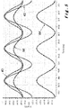
- Figure 4 illustrates plots of the voltage at gate aa of transistor M1 (line 50), the voltage at gate a of transistor M3 (line 52), and the bias voltage (line 54) applied to the bias node 40 for circuit 30 shown in Figure 3 . It will be appreciated that the voltages are the same for gate bb of transistor M2 and gate b of transistor M4 as transistors M2 and M4 are identical to transistors M1 and M3.
- Figure 5 illustrates plots of the transistor voltages for transistors M1 and M3 for the circuit 30 shown in Figure 3 .
- the transistor voltages for transistors M2 and M4 are identical to respective ones of those for transistors M1 and M3.
- the gate/source voltage Vgs and the gate/drain voltage Vds for transistor M3 are shown by lines 60 and 62 respectively.
- the gate/source voltage Vgs and the gate/drain voltage Vgd for transistor M1 are shown by lines 64 and 66 respectively. It can be seen that the Vgs for transistor M3 is twice that of the Vgs for transistor M1 but the Vgd voltages are approximately the same for transistors M1 and M3. As a result of the difference in Vgs for transistors M3 and M1, transistor M3 can easily be destroyed by a high voltage swing.
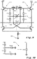
- FIG. 6 A schematic illustration of a differential Colpitts oscillator circuit 10 according to the present invention is shown in Figure 6 which illustrates how a low power supply voltage may be implemented to address the issues with circuit 30 shown in Figure 3 and described with reference to Figures 4 and 5 above.
- the circuit 100 is similar to that shown in Figure 3 and comprises two portions 110, 120. Each portion 110, 120 comprises its own power supply VDD with variable or tunable capacitor C2 being shared therebetween as before.
- Portion 110 includes transistor M1 and transistor M3 connected in series with a resistor R to ground 130, and inductor L a connected to gate aa of transistor M1. The inductor L a is connected between the gate aa of transistor M1 and point 140 to which a bias voltage Vbias can be applied as shown.
- portion 120 includes transistor M2 and transistor M4 connected in series with the resistor R to ground 130 and inductor L connected to gate bb of transistor M2.
- the inductor L b is connected between gate bb of transistor M2 and the point 140 to which the bias voltage Vbias can be applied as shown.
- Variable or tunable capacitor C2 is connected between each of the transistor pairs M1, M3 and M2, M4 as shown at tap points 150, 160.
- Capacitor C1 a in portion 110 is connected to line 170 between inductor L a and gate aa of transistor M1 at one end and to line 180 between tap points 150, 160, including the variable or tunable capacitor C2, at the other end.
- capacitor C1 in portion 120 is connected to line 180 between inductor L b and gate bb of transistor M2 at one end and to line 190 between tap points 150, 160 at the other end.
- Gate a of transistor M4 is connected to a centre-tap point A of the inductor L a in the other portion 110 of the circuit 100, and, gate b of transistor M3 is connected to a centre-tap point B of the inductor L b in the other portion 120 of the circuit 100, that is, the inductors L a , L b are crosscoupled with the gates a, b of transistors M3, M4 as shown.
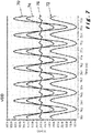
- Figure 7 is similar to Figure 4 but illustrates the plots for the voltages at gate aa of transistor M1 (line 70), at gate a of transistor M4 (line 72), at gate b of transistor M3 (line 74) and the bias voltage applied to point 140 (line 76).
- the plots of the voltage at gate bb of transistor M2 will be identical to that shown by line 70.
- Figure 8 is similar to Figure 5 illustrating the voltages for transistors M1 and M3.
- the transistor voltages for transistors M2 and M4 are identical to respective ones of those for transistors M1 and M3.
- the gate/source voltage Vgs and the gate/drain voltage Vds for transistor M3 are shown by lines 80 and 82 respectively.
- the gate/source voltage Vgs and the gate/drain voltage Vgd for transistor M1 are shown by lines 84 and 86 respectively. It can be seen that both the Vgs and Vgd values for transistor M3 are now similar to those for transistor M1, and, transistor M3 will no longer be destroyed by high voltage swings. This means that the size of transistors M1 and M3 can be the same thereby saving area.
- the minimum bias voltage applied to point 140 is now no longer dependent on threshold voltage Vth, and, is now determined by the sum of Vds (for transistor M1) and Vds (for transistor M3). This provides an improvement of between around 100mV to 200mV.
- the voltage swing at gates aa, bb of respective transistors M1, M2 is much higher than that at sources of the associated transistors. As a result, the size of the transistors M3, M4 can be reduced, and an improved layout is achieved for the transistors M1, M2, M3 and M4.
- the circuit 200 is similar to that shown in Figure 3 but includes a capacitive ladder or voltage divider 300. As before, the circuit 200 comprises two portions 210, 220 each comprising its own power supply VDD with a variable capacitor C2' shared therebetween as before.
- Portion 210 includes transistor M1 and transistor M3 connected in series with a resistor R to ground 230, and inductor L a connected to gate aa of transistor M1.
- the inductor L a is connected between gate aa of transistor M1 and point 240 to which a bias voltage Vbias can be applied as shown.
- portion 220 includes transistor M2 and transistor M4 connected in series with the resistor R to ground 230 and inductor L b connected to gate bb of transistor M2.
- the inductor L b is connected between gate bb of transistor M2 and the point 240 to which the bias voltage Vbias can be applied as shown.
- Gate a of transistor M4 is connected to a centre-tap point A of the inductor L a in the other portion 210 of the circuit 200, and, gate b of transistor M3 is connected to a centre-tap point B of the inductor L b in the other portion 220 of the circuit 200, that is, the inductors L a , L b are crosscoupled with the gates a, b of transistors M3, M4 as shown.
- Variable capacitor C2' is connected between each of the transistor pairs M1, M3 and M2, M4 as shown at tap points 250, 260.
- the single capacitor C1 a , C1 b is replaced by capacitors C1 a , C1 b and C3 a , C3 b arranged in series between line 270 and line 280 in portion 210 and between line 290 and line 280 in portion 220 as shown.
- the capacitive ladder or voltage divider 300 comprises capacitors C1 a , C1 b and C3 a , C3 b in each of portions 210, 220 and a tunable capacitor Ctune' connected between tap point 310 in portion 210 and tap point 320 in portion 220 of circuit 200.
- the capacitance of capacitors C1 a , C1 b and C3 a , C3 b are and C 3 respectively (as capacitors C1 a and C1 b are identical, and, capacitors C3 a and C3 b are identical) with the capacitance of capacitor Ctune' as C tune / 2 and the capacitance of capacitor C2' as C 2 / 2.
- the capacitance value of each capacitor C2' and Ctune' is now halved.
- Figure 10 illustrates the effect of the capacitive ladder or voltage divider 300 where the effective capacitance thereof is C total . Only one end of of the capacitive ladder is shown which with the other end, provides a total effective capacitance of C total .
- the capacitive voltage divider 300 of Figure 9 provides positive feedback for the circuit 200.
- C 2 and C tune have equal impact on the total capacitance C total .
- C 2 and C tune correspond to C 2 ' and C tune ' respectively as shown in Figure 9 .
- capacitor C2' is a variable capacitor, it is proposed to use only capacitor Ctune' to effect the frequency tuning; but fine-tuning of the oscillator circuit can be achieved by tuning capacitor C2'.
- fine-tuning refers to making small precise adjustments in order to achieve the best or desired performance. This is in contrast to the term “tuning” which provides larger less precise adjustments.
Claims (5)
- Circuit d'oscillateur Collpitts différentiel (100 ; 200) comprenant :une première paire de transistors (M1, M3) présentant un premier point de branchement (150 ; 250) entre une source d'un transistor (M1) et un drain de l'autre transistor (M3) ;une première alimentation électrique (VDD) connectée à un premier transistor (M1) de la première paire de transistors (M1, M3) ;une première bobine d'induction (La) connectée dans une première ligne (170 ; 270) entre une grille (aa) du premier transistor (M1) de la première paire de transistors (M1, M3) et un point de connexion (140 ; 240) ;une seconde paire de transistors (M2, M4) présentant un second point de branchement (160 ; 260) entre une source d'un transistor (M2) et un drain de l'autre transistor (M4) ;une seconde alimentation électrique (VDD) connectée à un premier transistor (M2) de la seconde paire de transistors (M2, M4) ;une seconde bobine d'induction (Lb) connectée dans une deuxième ligne (190 ; 290) entre une grille (bb) du premier transistor (M2) de la seconde paire de transistors (M2, M4) et le point de connexion (140 ; 240) ;un premier condensateur variable (C2 ; C2') connecté dans une troisième ligne (180; 280) entre les premier et second points de branchement (150, 160 ; 250, 260) ; etune résistance (R) connectée à un second transistor (M3) de la première paire de transistors (M1, M3) et à un second transistor (M4) de la seconde paire de transistors (M2, M4), la résistance étant également connectée à un point de masse (130 ; 230) ;caractérisé en ce qu'une grille (a) du second transistor (M4) de la seconde paire de transistors (M2, M4) est connectée à un premier point de branchement (A) de la première bobine d'induction (La) et qu'une grille (b) du second transistor (M3) de la première paire de transistors (M1, M3) est connectée à un second point de branchement (B) de la seconde bobine d'induction (Lb).
- Circuit selon la revendication 1, dans lequel les premier et second points de branchement (A, B) comprennent des points de branchement centraux.
- Circuit selon la revendication 1 ou 2, comprenant en outre un diviseur de tension capacitif (300) connecté entre la troisième ligne (280) et une ligne entre la grille (aa) du premier transistor (M1) de la première paire de transistors (M1, M3) et la grille (bb) du premier transistor (M2) de la seconde paire de transistors (M2, M4), le condensateur variable (C2') faisant partie du diviseur de tension capacitif.
- Circuit selon la revendication 3, dans lequel le diviseur de tension (300) comprend :au moins une première paire de condensateurs (C1a, C3a) connectés entre la grille (aa) du premier transistor (M1) de la première paire de transistors (M1, M3) dans la première ligne (270) et le premier point de branchement (250) dans la troisième ligne (280) ;au moins une seconde paire de condensateurs (C1b, C3b) connectés entre la grille (bb) du premier transistor (M2) de la seconde paire de transistors (M2, M4) dans la deuxième ligne (290) et le second point de branchement (260) dans la troisième ligne (280) ; etun second condensateur variable (Ctune') connecté entre des points intermédiaires (310, 320) des première et seconde paires de condensateurs (C1a, C3a, C1b, C3b) et conçu pour déterminer une plage de réglage du circuit.
- Circuit selon la revendication 4, dans lequel le premier condensateur variable (C2') est conçu pour le réglage fin du circuit.
Priority Applications (2)
| Application Number | Priority Date | Filing Date | Title |
|---|---|---|---|
| EP18186506.4A EP3605839B1 (fr) | 2018-07-31 | 2018-07-31 | Perfectionnements apportés ou se rapportant à des oscillateur colpitts |
| US16/527,799 US10819278B2 (en) | 2018-07-31 | 2019-07-31 | Oscillator circuit |
Applications Claiming Priority (1)
| Application Number | Priority Date | Filing Date | Title |
|---|---|---|---|
| EP18186506.4A EP3605839B1 (fr) | 2018-07-31 | 2018-07-31 | Perfectionnements apportés ou se rapportant à des oscillateur colpitts |
Publications (2)
| Publication Number | Publication Date |
|---|---|
| EP3605839A1 EP3605839A1 (fr) | 2020-02-05 |
| EP3605839B1 true EP3605839B1 (fr) | 2021-01-13 |
Family
ID=63108471
Family Applications (1)
| Application Number | Title | Priority Date | Filing Date |
|---|---|---|---|
| EP18186506.4A Active EP3605839B1 (fr) | 2018-07-31 | 2018-07-31 | Perfectionnements apportés ou se rapportant à des oscillateur colpitts |
Country Status (2)
| Country | Link |
|---|---|
| US (1) | US10819278B2 (fr) |
| EP (1) | EP3605839B1 (fr) |
Families Citing this family (1)
| Publication number | Priority date | Publication date | Assignee | Title |
|---|---|---|---|---|
| CN116210151A (zh) * | 2020-09-28 | 2023-06-02 | 华为技术有限公司 | 使用开关电感器的宽带低相位噪声数控振荡器 |
Family Cites Families (7)
| Publication number | Priority date | Publication date | Assignee | Title |
|---|---|---|---|---|
| US8143960B2 (en) * | 2008-01-25 | 2012-03-27 | Broadcom Corporation | Voltage controlled oscillator with multi-tap inductor |
| US7834712B2 (en) | 2008-10-09 | 2010-11-16 | Altera Corporation | Techniques for providing option conductors to connect components in an oscillator circuit |
| TWI398094B (zh) * | 2010-05-04 | 2013-06-01 | Univ Nat Chiao Tung | 雙正回授壓控震盪器 |
| JP5975912B2 (ja) * | 2013-03-18 | 2016-08-23 | ルネサスエレクトロニクス株式会社 | 高周波信号処理装置 |
| US9397613B2 (en) * | 2014-10-03 | 2016-07-19 | Short Circuit Technologies Llc | Switching current source radio frequency oscillator |
| US9425737B1 (en) * | 2015-03-16 | 2016-08-23 | Futurewei Technologies, Inc. | Tapped inductor voltage controlled oscillator |
| US10355643B2 (en) * | 2016-12-15 | 2019-07-16 | Korea Advanced Institute Of Science And Technology | Differential Colpitts voltage-controlled oscillator |
-
2018
- 2018-07-31 EP EP18186506.4A patent/EP3605839B1/fr active Active
-
2019
- 2019-07-31 US US16/527,799 patent/US10819278B2/en active Active
Non-Patent Citations (1)
| Title |
|---|
| None * |
Also Published As
| Publication number | Publication date |
|---|---|
| EP3605839A1 (fr) | 2020-02-05 |
| US20200044606A1 (en) | 2020-02-06 |
| US10819278B2 (en) | 2020-10-27 |
Similar Documents
| Publication | Publication Date | Title |
|---|---|---|
| US7522007B2 (en) | Injection locked frequency divider | |
| US20180019757A1 (en) | Passive phased injection locked circuit | |
| US8665030B2 (en) | Voltage-controlled oscillator | |
| US8035457B2 (en) | Voltage controlled oscillator | |
| US20060220754A1 (en) | Voltage controlled oscillator | |
| US20080309423A1 (en) | Voltage control oscillator and oscillation control system | |
| US8035456B1 (en) | Multi-phase signal generator and voltage-controlled oscillator thereof | |
| EP3605839B1 (fr) | Perfectionnements apportés ou se rapportant à des oscillateur colpitts | |
| US20080315964A1 (en) | Voltage controlled oscillator using tunable active inductor | |
| EP3605838B1 (fr) | Perfectionnements apportés ou se rapportant à des oscillateur colpitts | |
| JP2010278658A (ja) | 電圧制御発振器 | |
| US6819193B2 (en) | Method and circuitry for implementing a differentially tuned varactor-inductor oscillator | |
| US9520829B1 (en) | Apparatus and method of fine capacitance tuning for high resolution digitally controlled oscillator | |
| US10326459B1 (en) | Injection locked frequency divider | |
| KR101678786B1 (ko) | Rf 부성 저항 탱크와 트랜스포머 피드백을 이용한 주입동기 주파수 분배기 | |
| US20130141178A1 (en) | Injection Locked Divider with Injection Point Located at a Tapped Inductor | |
| Ghorbel et al. | Ultra low power RF cross-coupled VCO design in the subthreshold regime with high immunity to PVT variations in 130nm CMOS technology | |
| US11239795B2 (en) | Fully integrated oscillator for ultra low voltage applications with quadrupled voltage and low phase noise | |
| KR101478949B1 (ko) | 트랜스포머와 전류 재사용 방식을 사용한 암스트롱 및 암스트롱 콜핏츠 전압 제어 발진기 | |
| CN110719070A (zh) | 一种基于动态阈值技术的低功耗压控振荡器 | |
| US20010035797A1 (en) | Method and circuitry for implementing a differentially tuned varactor-inductor oscillator | |
| CN111342774A (zh) | 一种基于c类振荡器拓扑的双核压控振荡器 | |
| EP3190707A1 (fr) | Oscillateur à fréquence variable ayant une large plage d'accord et un faible bruit de phase | |
| Ghorbel et al. | Optimization of voltage-controlled oscillator VCO using current-reuse technique | |
| KR101563408B1 (ko) | 저 전력과 저 위상 잡음의 특성을 가지는 컴플리멘터리 콜피츠 전압 제어 발진기 |
Legal Events
| Date | Code | Title | Description |
|---|---|---|---|
| PUAI | Public reference made under article 153(3) epc to a published international application that has entered the european phase |
Free format text: ORIGINAL CODE: 0009012 |
|
| STAA | Information on the status of an ep patent application or granted ep patent |
Free format text: STATUS: THE APPLICATION HAS BEEN PUBLISHED |
|
| AK | Designated contracting states |
Kind code of ref document: A1 Designated state(s): AL AT BE BG CH CY CZ DE DK EE ES FI FR GB GR HR HU IE IS IT LI LT LU LV MC MK MT NL NO PL PT RO RS SE SI SK SM TR |
|
| AX | Request for extension of the european patent |
Extension state: BA ME |
|
| STAA | Information on the status of an ep patent application or granted ep patent |
Free format text: STATUS: REQUEST FOR EXAMINATION WAS MADE |
|
| 17P | Request for examination filed |
Effective date: 20200612 |
|
| RBV | Designated contracting states (corrected) |
Designated state(s): AL AT BE BG CH CY CZ DE DK EE ES FI FR GB GR HR HU IE IS IT LI LT LU LV MC MK MT NL NO PL PT RO RS SE SI SK SM TR |
|
| GRAP | Despatch of communication of intention to grant a patent |
Free format text: ORIGINAL CODE: EPIDOSNIGR1 |
|
| STAA | Information on the status of an ep patent application or granted ep patent |
Free format text: STATUS: GRANT OF PATENT IS INTENDED |
|
| INTG | Intention to grant announced |
Effective date: 20201020 |
|
| GRAS | Grant fee paid |
Free format text: ORIGINAL CODE: EPIDOSNIGR3 |
|
| GRAA | (expected) grant |
Free format text: ORIGINAL CODE: 0009210 |
|
| STAA | Information on the status of an ep patent application or granted ep patent |
Free format text: STATUS: THE PATENT HAS BEEN GRANTED |
|
| AK | Designated contracting states |
Kind code of ref document: B1 Designated state(s): AL AT BE BG CH CY CZ DE DK EE ES FI FR GB GR HR HU IE IS IT LI LT LU LV MC MK MT NL NO PL PT RO RS SE SI SK SM TR |
|
| REG | Reference to a national code |
Ref country code: GB Ref legal event code: FG4D |
|
| REG | Reference to a national code |
Ref country code: CH Ref legal event code: EP |
|
| REG | Reference to a national code |
Ref country code: IE Ref legal event code: FG4D |
|
| REG | Reference to a national code |
Ref country code: DE Ref legal event code: R096 Ref document number: 602018011763 Country of ref document: DE |
|
| REG | Reference to a national code |
Ref country code: AT Ref legal event code: REF Ref document number: 1355306 Country of ref document: AT Kind code of ref document: T Effective date: 20210215 |
|
| REG | Reference to a national code |
Ref country code: AT Ref legal event code: MK05 Ref document number: 1355306 Country of ref document: AT Kind code of ref document: T Effective date: 20210113 |
|
| REG | Reference to a national code |
Ref country code: NL Ref legal event code: MP Effective date: 20210113 |
|
| REG | Reference to a national code |
Ref country code: LT Ref legal event code: MG9D |
|
| PG25 | Lapsed in a contracting state [announced via postgrant information from national office to epo] |
Ref country code: FI Free format text: LAPSE BECAUSE OF FAILURE TO SUBMIT A TRANSLATION OF THE DESCRIPTION OR TO PAY THE FEE WITHIN THE PRESCRIBED TIME-LIMIT Effective date: 20210113 Ref country code: HR Free format text: LAPSE BECAUSE OF FAILURE TO SUBMIT A TRANSLATION OF THE DESCRIPTION OR TO PAY THE FEE WITHIN THE PRESCRIBED TIME-LIMIT Effective date: 20210113 Ref country code: GR Free format text: LAPSE BECAUSE OF FAILURE TO SUBMIT A TRANSLATION OF THE DESCRIPTION OR TO PAY THE FEE WITHIN THE PRESCRIBED TIME-LIMIT Effective date: 20210414 Ref country code: BG Free format text: LAPSE BECAUSE OF FAILURE TO SUBMIT A TRANSLATION OF THE DESCRIPTION OR TO PAY THE FEE WITHIN THE PRESCRIBED TIME-LIMIT Effective date: 20210413 Ref country code: PT Free format text: LAPSE BECAUSE OF FAILURE TO SUBMIT A TRANSLATION OF THE DESCRIPTION OR TO PAY THE FEE WITHIN THE PRESCRIBED TIME-LIMIT Effective date: 20210513 Ref country code: NO Free format text: LAPSE BECAUSE OF FAILURE TO SUBMIT A TRANSLATION OF THE DESCRIPTION OR TO PAY THE FEE WITHIN THE PRESCRIBED TIME-LIMIT Effective date: 20210413 Ref country code: LT Free format text: LAPSE BECAUSE OF FAILURE TO SUBMIT A TRANSLATION OF THE DESCRIPTION OR TO PAY THE FEE WITHIN THE PRESCRIBED TIME-LIMIT Effective date: 20210113 |
|
| PG25 | Lapsed in a contracting state [announced via postgrant information from national office to epo] |
Ref country code: RS Free format text: LAPSE BECAUSE OF FAILURE TO SUBMIT A TRANSLATION OF THE DESCRIPTION OR TO PAY THE FEE WITHIN THE PRESCRIBED TIME-LIMIT Effective date: 20210113 Ref country code: PL Free format text: LAPSE BECAUSE OF FAILURE TO SUBMIT A TRANSLATION OF THE DESCRIPTION OR TO PAY THE FEE WITHIN THE PRESCRIBED TIME-LIMIT Effective date: 20210113 Ref country code: LV Free format text: LAPSE BECAUSE OF FAILURE TO SUBMIT A TRANSLATION OF THE DESCRIPTION OR TO PAY THE FEE WITHIN THE PRESCRIBED TIME-LIMIT Effective date: 20210113 Ref country code: AT Free format text: LAPSE BECAUSE OF FAILURE TO SUBMIT A TRANSLATION OF THE DESCRIPTION OR TO PAY THE FEE WITHIN THE PRESCRIBED TIME-LIMIT Effective date: 20210113 Ref country code: SE Free format text: LAPSE BECAUSE OF FAILURE TO SUBMIT A TRANSLATION OF THE DESCRIPTION OR TO PAY THE FEE WITHIN THE PRESCRIBED TIME-LIMIT Effective date: 20210113 |
|
| PG25 | Lapsed in a contracting state [announced via postgrant information from national office to epo] |
Ref country code: IS Free format text: LAPSE BECAUSE OF FAILURE TO SUBMIT A TRANSLATION OF THE DESCRIPTION OR TO PAY THE FEE WITHIN THE PRESCRIBED TIME-LIMIT Effective date: 20210513 |
|
| REG | Reference to a national code |
Ref country code: DE Ref legal event code: R097 Ref document number: 602018011763 Country of ref document: DE |
|
| PG25 | Lapsed in a contracting state [announced via postgrant information from national office to epo] |
Ref country code: SM Free format text: LAPSE BECAUSE OF FAILURE TO SUBMIT A TRANSLATION OF THE DESCRIPTION OR TO PAY THE FEE WITHIN THE PRESCRIBED TIME-LIMIT Effective date: 20210113 Ref country code: EE Free format text: LAPSE BECAUSE OF FAILURE TO SUBMIT A TRANSLATION OF THE DESCRIPTION OR TO PAY THE FEE WITHIN THE PRESCRIBED TIME-LIMIT Effective date: 20210113 Ref country code: CZ Free format text: LAPSE BECAUSE OF FAILURE TO SUBMIT A TRANSLATION OF THE DESCRIPTION OR TO PAY THE FEE WITHIN THE PRESCRIBED TIME-LIMIT Effective date: 20210113 |
|
| PLBE | No opposition filed within time limit |
Free format text: ORIGINAL CODE: 0009261 |
|
| STAA | Information on the status of an ep patent application or granted ep patent |
Free format text: STATUS: NO OPPOSITION FILED WITHIN TIME LIMIT |
|
| PG25 | Lapsed in a contracting state [announced via postgrant information from national office to epo] |
Ref country code: SK Free format text: LAPSE BECAUSE OF FAILURE TO SUBMIT A TRANSLATION OF THE DESCRIPTION OR TO PAY THE FEE WITHIN THE PRESCRIBED TIME-LIMIT Effective date: 20210113 Ref country code: DK Free format text: LAPSE BECAUSE OF FAILURE TO SUBMIT A TRANSLATION OF THE DESCRIPTION OR TO PAY THE FEE WITHIN THE PRESCRIBED TIME-LIMIT Effective date: 20210113 Ref country code: RO Free format text: LAPSE BECAUSE OF FAILURE TO SUBMIT A TRANSLATION OF THE DESCRIPTION OR TO PAY THE FEE WITHIN THE PRESCRIBED TIME-LIMIT Effective date: 20210113 |
|
| 26N | No opposition filed |
Effective date: 20211014 |
|
| PG25 | Lapsed in a contracting state [announced via postgrant information from national office to epo] |
Ref country code: AL Free format text: LAPSE BECAUSE OF FAILURE TO SUBMIT A TRANSLATION OF THE DESCRIPTION OR TO PAY THE FEE WITHIN THE PRESCRIBED TIME-LIMIT Effective date: 20210113 Ref country code: ES Free format text: LAPSE BECAUSE OF FAILURE TO SUBMIT A TRANSLATION OF THE DESCRIPTION OR TO PAY THE FEE WITHIN THE PRESCRIBED TIME-LIMIT Effective date: 20210113 |
|
| PG25 | Lapsed in a contracting state [announced via postgrant information from national office to epo] |
Ref country code: SI Free format text: LAPSE BECAUSE OF FAILURE TO SUBMIT A TRANSLATION OF THE DESCRIPTION OR TO PAY THE FEE WITHIN THE PRESCRIBED TIME-LIMIT Effective date: 20210113 |
|
| REG | Reference to a national code |
Ref country code: CH Ref legal event code: PL |
|
| PG25 | Lapsed in a contracting state [announced via postgrant information from national office to epo] |
Ref country code: MC Free format text: LAPSE BECAUSE OF FAILURE TO SUBMIT A TRANSLATION OF THE DESCRIPTION OR TO PAY THE FEE WITHIN THE PRESCRIBED TIME-LIMIT Effective date: 20210113 |
|
| REG | Reference to a national code |
Ref country code: BE Ref legal event code: MM Effective date: 20210731 |
|
| PG25 | Lapsed in a contracting state [announced via postgrant information from national office to epo] |
Ref country code: LI Free format text: LAPSE BECAUSE OF NON-PAYMENT OF DUE FEES Effective date: 20210731 Ref country code: IT Free format text: LAPSE BECAUSE OF FAILURE TO SUBMIT A TRANSLATION OF THE DESCRIPTION OR TO PAY THE FEE WITHIN THE PRESCRIBED TIME-LIMIT Effective date: 20210113 Ref country code: CH Free format text: LAPSE BECAUSE OF NON-PAYMENT OF DUE FEES Effective date: 20210731 |
|
| PG25 | Lapsed in a contracting state [announced via postgrant information from national office to epo] |
Ref country code: IS Free format text: LAPSE BECAUSE OF FAILURE TO SUBMIT A TRANSLATION OF THE DESCRIPTION OR TO PAY THE FEE WITHIN THE PRESCRIBED TIME-LIMIT Effective date: 20210513 Ref country code: LU Free format text: LAPSE BECAUSE OF NON-PAYMENT OF DUE FEES Effective date: 20210731 Ref country code: FR Free format text: LAPSE BECAUSE OF NON-PAYMENT OF DUE FEES Effective date: 20210731 |
|
| PG25 | Lapsed in a contracting state [announced via postgrant information from national office to epo] |
Ref country code: IE Free format text: LAPSE BECAUSE OF NON-PAYMENT OF DUE FEES Effective date: 20210731 Ref country code: BE Free format text: LAPSE BECAUSE OF NON-PAYMENT OF DUE FEES Effective date: 20210731 |
|
| GBPC | Gb: european patent ceased through non-payment of renewal fee |
Effective date: 20220731 |
|
| PG25 | Lapsed in a contracting state [announced via postgrant information from national office to epo] |
Ref country code: GB Free format text: LAPSE BECAUSE OF NON-PAYMENT OF DUE FEES Effective date: 20220731 |
|
| P01 | Opt-out of the competence of the unified patent court (upc) registered |
Effective date: 20230513 |
|
| PG25 | Lapsed in a contracting state [announced via postgrant information from national office to epo] |
Ref country code: NL Free format text: LAPSE BECAUSE OF NON-PAYMENT OF DUE FEES Effective date: 20210113 Ref country code: CY Free format text: LAPSE BECAUSE OF FAILURE TO SUBMIT A TRANSLATION OF THE DESCRIPTION OR TO PAY THE FEE WITHIN THE PRESCRIBED TIME-LIMIT Effective date: 20210113 |
|
| PG25 | Lapsed in a contracting state [announced via postgrant information from national office to epo] |
Ref country code: HU Free format text: LAPSE BECAUSE OF FAILURE TO SUBMIT A TRANSLATION OF THE DESCRIPTION OR TO PAY THE FEE WITHIN THE PRESCRIBED TIME-LIMIT; INVALID AB INITIO Effective date: 20180731 |
|
| PGFP | Annual fee paid to national office [announced via postgrant information from national office to epo] |
Ref country code: DE Payment date: 20230620 Year of fee payment: 6 |