EP3605815B1 - Verfahren zur berechnung der eingangsleistung und diese benutzende elektrische leistungssysteme - Google Patents
Verfahren zur berechnung der eingangsleistung und diese benutzende elektrische leistungssysteme Download PDFInfo
- Publication number
- EP3605815B1 EP3605815B1 EP19189622.4A EP19189622A EP3605815B1 EP 3605815 B1 EP3605815 B1 EP 3605815B1 EP 19189622 A EP19189622 A EP 19189622A EP 3605815 B1 EP3605815 B1 EP 3605815B1
- Authority
- EP
- European Patent Office
- Prior art keywords
- slope
- intercept
- values
- constant
- compensation
- Prior art date
- Legal status (The legal status is an assumption and is not a legal conclusion. Google has not performed a legal analysis and makes no representation as to the accuracy of the status listed.)
- Active
Links
Images


Classifications
-
- H—ELECTRICITY
- H02—GENERATION; CONVERSION OR DISTRIBUTION OF ELECTRIC POWER
- H02M—APPARATUS FOR CONVERSION BETWEEN AC AND AC, BETWEEN AC AND DC, OR BETWEEN DC AND DC, AND FOR USE WITH MAINS OR SIMILAR POWER SUPPLY SYSTEMS; CONVERSION OF DC OR AC INPUT POWER INTO SURGE OUTPUT POWER; CONTROL OR REGULATION THEREOF
- H02M1/00—Details of apparatus for conversion
- H02M1/42—Circuits or arrangements for compensating for or adjusting power factor in converters or inverters
- H02M1/4208—Arrangements for improving power factor of AC input
- H02M1/4225—Arrangements for improving power factor of AC input using a non-isolated boost converter
-
- G—PHYSICS
- G01—MEASURING; TESTING
- G01R—MEASURING ELECTRIC VARIABLES; MEASURING MAGNETIC VARIABLES
- G01R21/00—Arrangements for measuring electric power or power factor
- G01R21/133—Arrangements for measuring electric power or power factor by using digital technique
-
- G—PHYSICS
- G01—MEASURING; TESTING
- G01R—MEASURING ELECTRIC VARIABLES; MEASURING MAGNETIC VARIABLES
- G01R21/00—Arrangements for measuring electric power or power factor
- G01R21/006—Measuring power factor
-
- H—ELECTRICITY
- H02—GENERATION; CONVERSION OR DISTRIBUTION OF ELECTRIC POWER
- H02M—APPARATUS FOR CONVERSION BETWEEN AC AND AC, BETWEEN AC AND DC, OR BETWEEN DC AND DC, AND FOR USE WITH MAINS OR SIMILAR POWER SUPPLY SYSTEMS; CONVERSION OF DC OR AC INPUT POWER INTO SURGE OUTPUT POWER; CONTROL OR REGULATION THEREOF
- H02M1/00—Details of apparatus for conversion
- H02M1/0003—Details of control, feedback or regulation circuits
- H02M1/0012—Control circuits using digital or numerical techniques
-
- Y—GENERAL TAGGING OF NEW TECHNOLOGICAL DEVELOPMENTS; GENERAL TAGGING OF CROSS-SECTIONAL TECHNOLOGIES SPANNING OVER SEVERAL SECTIONS OF THE IPC; TECHNICAL SUBJECTS COVERED BY FORMER USPC CROSS-REFERENCE ART COLLECTIONS [XRACs] AND DIGESTS
- Y02—TECHNOLOGIES OR APPLICATIONS FOR MITIGATION OR ADAPTATION AGAINST CLIMATE CHANGE
- Y02B—CLIMATE CHANGE MITIGATION TECHNOLOGIES RELATED TO BUILDINGS, e.g. HOUSING, HOUSE APPLIANCES OR RELATED END-USER APPLICATIONS
- Y02B70/00—Technologies for an efficient end-user side electric power management and consumption
- Y02B70/10—Technologies improving the efficiency by using switched-mode power supplies [SMPS], i.e. efficient power electronics conversion e.g. power factor correction or reduction of losses in power supplies or efficient standby modes
Definitions
- the present disclosure generally relates to the field of electrical power and energy measurement and metering.
- the present disclosure is directed to methods of calculating power input into a power factor correction stage, and electrical power systems utilizing same.
- a first conventional method calculates input power by determining the output power of an SSLD-driver unit and dividing it by the estimated efficiency of the unit.
- the output power of the unit is calculated using the direct current (DC) output voltages and currents.
- the efficiency estimation is based on a lookup table that is stored in flash memory of the microcontroller of the driver unit.
- a second method employs an additional power-metering integrated circuit (IC) and circuitry at the input of the unit.
- the power-metering IC samples the input alternating current (AC) voltage and current at very high frequency.
- the sampled input voltages and currents are then multiplied and averaged over a 60Hz mains cycle to determine the input power.
- This method offers high accuracy but increases the production cost of the manufacturer because it requires additional components and circuitry.
- a third method assumes a unity power factor and a pure sinusoidal input current.
- the peak value of the input current is then used to estimate the root mean square (RMS) of the input current.
- the RMS input voltage is estimated in the same fashion.
- the input power is then calculated by multiplying the RMS input voltage and the RMS input current.
- US 2016/190912 A1 discloses a method of measuring an input power of a power factor converter (PFC), which includes monitoring a rectified voltage signal from an input of the PFC, determining a pulse timing value of the PFC, determining the input power by multiplying the monitored rectified voltage with the pulse timing value of the PFC to form multiplied values, and accumulating the multiplied samples.
- PFC power factor converter
- US 2008/315852 A1 discloses a power factor controller that includes a voltage loop compensator producing a voltage compensation signal as a function of an output voltage of the power processing circuit.
- CN 101 764 528 A discloses a high power factor DCM Boost PFC converter.
- US 2010/246220 A1 discloses a power supply having a specified hold-up time to take an input voltage and convert it to an output voltage.
- US 2014/239741 A1 discloses a method for controlling the temperature of a semiconductor device on an inverter of a drive configured to drive an electrical machine.
- the present disclosure is directed to a method of measuring power input into a system that includes a power factor compensation (PFC) stage that includes a switch controlled by a switch controller.
- PFC power factor compensation
- the method includes the features according to claim 1. Additional features for advantageous embodiments are recited in the dependent claims thereto.
- the present disclosure is directed to a device.
- the device includes the features according to claim 8. Additional features for advantageous embodiments are recited in the dependent claims thereto.
- the present disclosure is directed to an electrical-power system that includes a power factor compensation (PFC) stage and that uses an input-power-estimating equation that simplifies the determination of the amount of power being input into the PFC stage.
- PFC power factor compensation
- the input-power-estimating equation is based on a slope-intercept simplification of a quadratic equation that provides an exact solution for the input power as a function of various parameters of the PFC stage.
- slope-intercept equation can be implemented very efficiently within, for example, a microcontroller that may already be available to control the PFC stage.
- an electrical-power system of the present disclosure can be used in any of many of a wide variety of commercial devices, including devices participating in the Internet of things (IoT).
- IoT Internet of things
- Those skilled in the art know that examples of such devices include, but are not limited to, industrial lighting drivers (e.g., drivers such as the OTi85 DALI, OTi60 DALI, OTi50 DALI, and OTi30 DALI available from OSRAM), household appliances with front-end PFC stage (such as smart LCD/LED TVs, laptop chargers, and cell-phone charges), among many others.
- industrial lighting drivers e.g., drivers such as the OTi85 DALI, OTi60 DALI, OTi50 DALI, and OTi30 DALI available from OSRAM
- household appliances with front-end PFC stage such as smart LCD/LED TVs, laptop chargers, and cell-phone charges
- the types of electrical-power systems in which aspects of the present disclosure may be implemented is limited only by the ability to apply the mathematical formulations
- FIG. 1 illustrates an example electrical-power system 100.
- the electrical-power system 100 includes a PFC stage 104 that has an input 108, which receives electrical power from an alternating current (AC) power source (not shown), and an output 112, which provides power to one or more loads (not shown).
- the power source and load(s) may be any power source and load(s) compatible with the electrical-power system 100.
- the PFC stage 104 includes a switch 116, such as a MOSFET, that controls the operation of the PFC stage 104.
- the PFC stage 104 may be, for example, a boost type stage or a flyback stage, and may operate in any suitable current conduction mode, i.e., a critical conduction mode, a continuous conduction mode, or a discontinuous conduction mode.
- a critical conduction mode boost-type PFC stage various equations are presented and derived below for an example critical conduction mode boost-type PFC stage.
- those equations can be adapted for other types of PFC stages; essentially, only the constants in the equations will change for differing types of PFC stages.
- Those skilled in the art will readily understand how to adapt the equations below to PFC stages other than the critical conduction mode boost-type PFC stage used to illustrate the basic principles of the methodologies applied herein.
- the electrical-power system 100 also includes a switch controller 120 that is in operative communication with the switch 116 of the PFC stage 104 so as to control the operation of the switch 116 and the PFC stage 104 in accordance with a switch control algorithm 124 suitable for the PFC device at issue.
- the switch controller 120 controls the gate of the MOSFET.
- Those skilled in the art will readily understand that another type of switch can be used for the switch 116, as well as the configuration of the switch controller 120 needed to control the switch.
- the electrical-power system 100 further includes a memory 128 and an input-power estimator 132 that is in operative communication with the memory 128 and the switch controller 120.
- the input-power estimator 132 is configured to solve a slope-intercept equation 136 that estimates the input power input into the PFC stage 104.
- the slope-intercept equation 136 is a function of the on-time of the switch 116 and the voltage input into the PFC stage 104, and includes a plurality of slope constants and a plurality of y-intercept constants (not illustrated).
- a detailed derivation of a slope-intercept equation suitable for use as the slope-intercept equation 136 is presented below relative to a critical conduction mode boost-type PFC stage.
- Values 140 of the slope constants and the y-intercept constants are stored in the memory 128 and retrieved by the input-power estimator 132 as needed to solve the slope-intercept equation 136.
- the slope-constant and y-intercept-constant values 140 can be determined for each instantiation of the PFC stage 104, since the operating characteristics of the PFC stage 104 can vary from one instantiation to another, for example, due to variability in the individual electronic elements (e.g., inductor(s), resistor(s), capacitor(s), switch(es), diode(s), etc.) that make up each particular instantiation.
- the input-power estimator 132 may optionally include a temperature compensator 144 that adjusts the slope-constant values 140A and the y-intercept-constant values 140B based on the temperature at which the PFC stage 104 is operating.
- the temperature compensator 144 utilizes a plurality of temperature-compensation constant values 148, namely, a plurality of slope-constant temperature-compensation constant values 148A and a plurality y-intercept-constant temperature-compensation constant values 148B, and a temperature differential 152 to determine a plurality of slope-constant temperature-compensation values and a plurality y-intercept-constant temperature-compensation values that are used to adjust the slope-constant values 140A and the y-intercept-constant values 140B for the current temperature of the electrical-power system 100.
- the plurality of temperature-compensation values 148 here, the plurality of slope-constant temperature-compensation constant values 148A and the plurality of y-intercept-constant temperature-compensation constant values 148B, are stored in the memory 128.
- the temperature differential 152 may be determined using a temperature estimator 156. Details of an example of implementing the temperature estimator 144 are described below.
- the memory 128 can be any one or more types of memory, such as non-volatile memory, among others.
- the switch controller 120 and the input-power estimator 132 may be implemented using any suitable hardware and/or software.
- the switch controller 120 and the input-power estimator 132 may be implemented in a single microcontroller (not shown), such as a microcontroller that may have otherwise been provided to implement the switch controller. If such a microcontroller implementation is used, the memory 128 may be located onboard the microcontroller.
- Microcontrollers are already used in many PFC applications to control the PFC stages. Consequently, implementing an input-power estimator of the present disclosure, such as input-power estimator 132 of FIG. 1 , in such a microcontroller would be straightforward in view of the present disclosure. No additional circuitry is required; generally only the firmware of the microcontroller needs to be updated. Therefore, the implementation cost to a manufacturer is minimal.
- the input-power estimator 132 includes an output device 160 to communicate, offboard the input-power estimator, the calculated input power input into the PFC device 104.
- the output device 160 may be any suitable wired device (e.g., communications port) or wireless device (e.g., radio-frequency or optical communication device), or any combination thereof.
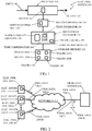
- FIG. 2 illustrates a simple scenario in which a number, N, of electronic devices 200(1) to 200(N) are in communication with a higher-level system 204 that utilizes input-power data 208(1) to 208(N) generated aboard the electronic devices.
- Each of the electronic devices 200(1) to 200(N) includes respective electrical-power systems 212(1) to 212(N) that are configured to generate the input-power data 208(1) to 208(N) in accordance with aspects disclosed herein.
- each electrical-power system 212(1) to 212(N) has the general configuration of the electrical-power system 100 of FIG. 1 and, therefore, generates the input-power data 208(1) to 208(N) in the manner described above and illustrated below.
- the higher-level system 204 may be configured to use the utilize power data 208(1) to 208(N) in any number of ways.
- the higher-level system 204 may be configured to collect the power data 208(1) to 208(N), use the power data 208(1) to 208(N) to make power-usage decisions, control the electronic devices 200(1) to 200(N) based on the power data 208(1) to 208(N), determine billing amounts for power consumption by the electronic devices 200(1) to 200(N), communicate the power data 208(1) to 208(N) and/or information derived therefrom to another system (not shown), and/or control one or more other electronic devices (not shown) based on the power data 208(1) to 208(N), among other things. As shown in FIG.
- each electrical-power system 212(1) to 212(N) is in operative communication with the higher-level system 204 via one or more data communications networks 216, which may be and/or include a local-area network, a wide-area network, a global network (such as the Internet), and a deep-space network, among others, and any combination thereof.
- data communications networks 216 may be and/or include a local-area network, a wide-area network, a global network (such as the Internet), and a deep-space network, among others, and any combination thereof.
- an electrical-power system is composed of a constant-voltage digital addressable lighting interface (DALI) device that includes a PFC stage that is of the boost type and has a critical conduction mode.
- DALI digital addressable lighting interface
- An example of such a DALI device is the OT50 DALI available from OSRAM.
- the DALI device is referred to as the "driver”.
- Table 1 below provides various nomenclature used throughout. Table 1 Variable Name Description u in Instantaneous input voltage of the PFC converter i in Instantaneous input current of the PFC converter p in Instantaneous input power of the PFC converter i L Instantaneous inductor current ⁇ Moving average operator. Averaging period is either over one mains cycle (60Hz in US) or over one switching cycle.
- Averaging period is specified in the context.
- P in ave Average input power over a mains cycle (60Hz in US)
- L Inductance of the inductor
- V d Voltage drop of a single diode in the diode bridge r d
- T Mains period (16.7ms in US)
- f sw Instantaneous switching frequency of the PFC switch t on Average on-time that is the output of the low-bandwidth PID controller
- T ref Reference temperature usually 25°
- b k Indexed coefficient for calculating the y-intercept b M k Indexed measured slope B k Indexed measured y-intercept S L P in , driver Sensitivity of the input power with respect to variations in the inductance of the inductor, in %/% unit m k ′ Indexed coefficient for calculating the slope m , modified to account for temperature variations. b k ′ Indexed coefficient for calculating the y-intercept b , modified to account for temperature variations. k m,i i th temperature coefficient used for calculating m i ′ . k b ,i i th temperature coefficient used for calculating b i ′ .
- the input current profile bounces between zero and the peak current value, i L,pk , in a piecewise fashion as shown in FIG. 3 .
- U out is the output voltage of the PFC boost converter, i.e. the rail voltage.
- the P in,ave in equation (11) does not consider the power loss in the diode bridge, which comes before the PFC.
- Equation (16) is a quadratic equation in terms of P in,driver . It can be solved for P in,driver , given U in,rms , t on , L , V d , r d , T, and a set of ⁇ S k ⁇ . It is obvious that implementation of equation (16) in the microcontroller of the PFC is impractical. Below there is described a practical way of tackling this highly nonlinear equation.
- P in , driver mt on + b
- m and b are the slope and y-intercept of the linear approximation.
- the input power measurement should be done for three different values of U in,rms that are between U in,rms (min) and U in,rms (max). In some embodiments, it is recommended that the chosen U in,rms values are not close to U in,rms (min) or U in,rms (max) because of high nonlinearity near the lower and upper limits. Then for each U in,rms , P in,driver is measured for different values of t on to obtain three different linear curves. An example set of t on versus P in,driver curves is shown in FIG. 4 for the example OT50 DALI mentioned above.
- FIG. 5 A circuit diagram of an example front-end boost-type PFC converter 500 is shown in FIG. 5 .
- the front-end boost-type PFC converter 500 includes a PFC stage 502 having a rectifying diode bridge 504, an inductor 508, a diode 512, a switch 516, and a capacitor 520 providing a filter.
- the front-end boost-type PFC converter 500 also includes a microcontroller 524 to control the gate 516A of the switch 516.
- the input to the rectifying diode bridge 504, i.e., the AC source (not shown) is put through an electromagnetic interference (EMI) filter 528, and the output is provided to a load, here, a point of load converters 532.
- EMI electromagnetic interference
- the input voltage, u in , the inductor 508 current's zero-current-detection (ZCD) signal, and the rail voltage, u rail , are measured and fed into the microcontroller 524, which generates a gate signal, q gate , for the switch 516.
- the fundamental operation of the PFC stage 502 in providing power factor correction is the same as the operation of conventional PFC stages, such that further explanations of that aspect of the PFC stage 502 and the microcontroller 524 are not necessary for those skilled in the art to understand the scope of the present disclosure.
- FIG. 6 is a diagram of the microcontroller 524 of FIG. 5 that depicts a closed-loop switch controller 600 to control the gate 516A of the switch 516 of FIG. 5 and an input-power estimator 604 that estimates the power input, P * in , into the front-end boost-type PFC converter 500.
- the closed-loop switch controller 600 includes a PID compensator 608 and a pulse-width modulated (PWM) generator 612.
- the PID compensator 608 operates on the difference between the rail voltage u rail and a reference voltage, U ref .
- the output of the PID compensator 608, i.e., u PID is the reference on-time, t on , for the switch 516 of FIG. 5 , because if the rail voltage u rail is less than the reference voltage U ref then t on must be increased and vice versa.
- the PWM generator 612 utilizes t on and an inductor current i L to generate a gate signal q gate .
- the input-power estimator 604 is configured to solve equation (21) to calculate an estimated power P * in , which is equivalent to the P in,driver of equation (21).
- values of slope constants m 1 , m 2 , and m 3 and y-intercept constants b 1 , b 2 , and b 3 are stored in a memory 616 of the microcontroller 524.
- the estimated input power, P* in can be used for energy metering purpose if it is multiplied by the time-interval between subsequent P * in calculations.
- the purpose of the automated calibration procedure is to produce the parameters of the model described in equation (21), i.e., m 1 , m 2 , m 3 , b 1 , b 2 , and b 3 .
- At least nine operating points are required for three different input voltages, ⁇ U in,rms,1 , U in,rms,2 , U in,rms,3 ⁇ , and three different input powers, ⁇ P in,driver,1 , P in,driver,2 , P in,driver,3 ⁇ .
- the more operating points used for calibration the more accurate the parameters would be. In some embodiments, it is recommended that eighteen operating points are employed for optimum accuracy (three input voltages and six input powers).
- These formulas can be embedded in an automatic calibration device to accelerate the production line.
- Step 6 The calculated values for the slope constants, m 1 , m 2 , m 3 , and the y-intercept constants b 1 , b 2 , b 3 , are loaded in, for example, an EEPROM of a microcontroller for a PFC stage.
- Equation (21) An important issue regarding the model represented by equation (21) is to address how much the tolerances of the electronic components in different units can affect the parameters of this model. This is important in determining whether one set of values for the slope and y-intercept constants can be used every manufactured device of the same type or whether each device needs to be calibrated by itself.
- the main circuit component that affects the formula for calculating the input power in equation (16) is an inductor of a PFC stage.
- the parameters of the diode bridge, V d and r d can also affect the formula, but their contributions are minimal compared to that of the L .
- a 5% change in L will translate to -5% change in the measured input power. Since the tolerance of the magnetic components is always around 5% to 10%, it may be desirable to calibrate each unit by itself during the manufacturing process.
- the following subsections describe an example temperature calibration method for reducing temperature-induced error.
- equation set (32) the terms k m1 ⁇ T , k m2 ⁇ T, and k m3 ⁇ T are referred to as “slope-constant temperature-compensation values", and the terms k b1 ⁇ T , k b2 ⁇ T, and k b3 ⁇ T are referred to as "y-intercept-constant temperature-compensation values”.
- the first step in finding the temperature compensation constants is to populate this table.
- U in,rms(1) U in,rms (min)
- U in , rms(2) 0.5 U in,rms (min) + 0.5 U in,rms (max)
- ⁇ M 1 ⁇ T M 1 T max ⁇ M 1 T ref
- M 2 ⁇ T M 2 T max ⁇ M 2 T ref
- M 3 ⁇ T M 3 T max ⁇ M 3 T ref
- B 1 ⁇ T B 1 T max ⁇ B 1 T ref
- B 2 ⁇ T B 2 T max ⁇ B 2 T ref
- B 3 ⁇ T B 3 T max ⁇ B 3 T ref
- ⁇ T T max ⁇ T ref
- FIG. 7 illustrates a microcontroller 700 that includes temperature compensation as described immediately above.
- the microcontroller 700 is a modified version of the microcontroller 524 of FIG. 6 .
- the microcontroller 700 of FIG. 7 includes the same closed-loop switch controller 600 and essentially the same input-power estimator 604 of the microcontroller 524 of FIG. 6 , but an input-power estimator 704 of the microcontroller 700 is augmented with a temperature compensator 708.
- the temperature compensator 708 includes a temperature estimator 712 that generates a temperature estimate, T est , and a difference calculator 716 that calculates a difference, ⁇ T , between T est and a reference temperature, T ref .
- the temperature estimator 712 is of the negative-temperature coefficient (NTC) type, but it could be of another type, such as a positive-temperature coefficient type.
- the temperature estimator 712 is configured to modify the plurality of slope-constant values ⁇ m 1 , m 2 , m 3 ⁇ and the plurality y-intercept-constant values ⁇ b 1 , b 2 , b 3 ⁇ using the plurality of slope-constant temperature-compensation constant values ⁇ k m1 , k m2 , k m3 ⁇ , the plurality of y-intercept-constant temperature compensation constant values ⁇ k b1 , k b2 , k b3 ⁇ , and ⁇ T as indicated in equation set (32) to generate corresponding respective temperature-compensated slope-constant values ⁇ m ' 1 , m' 2 , m' 3 ⁇ and temperature-compensated y-intercept-constant values ⁇ b' 1 , b' 2 , b ' 3 ⁇ , which are then used to determine P in * in accordance with equation (31), with P in * being equivalent to
- the methods and systems described herein are not limited to a particular hardware or software configuration, and may find applicability in many computing or processing environments.
- the methods and systems may be implemented in hardware or software, or a combination of hardware and software.
- the methods and systems may be implemented in one or more computer programs, where a computer program may be understood to include one or more processor executable instructions.
- the computer program(s) may execute on one or more programmable processors, and may be stored on one or more storage medium readable by the processor (including volatile and non-volatile memory and/or storage elements), one or more input devices, and/or one or more output devices.
- the processor thus may access one or more input devices to obtain input data, and may access one or more output devices to communicate output data.
- the input and/ or output devices may include one or more of the following: Random Access Memory (RAM), Redundant Array of Independent Disks (RAID), floppy drive, CD, DVD, Blu-Ray, magnetic disk, internal hard drive, external hard drive, memory stick, flash drive, solid state memory device, or other storage device capable of being accessed by a processor as provided herein, where such aforementioned examples are not exhaustive, and are for illustration and not limitation.
- RAM Random Access Memory
- RAID Redundant Array of Independent Disks
- floppy drive CD, DVD, Blu-Ray, magnetic disk, internal hard drive, external hard drive, memory stick, flash drive, solid state memory device, or other storage device capable of being accessed by a processor as provided herein, where such aforementioned examples are not exhaustive, and are for illustration and not limitation.
- the computer program(s) may be implemented using one or more high level procedural or object-oriented programming languages to communicate with a computer system; however, the program(s) may be implemented in assembly or machine language, if desired.
- the language may be compiled or interpreted.
- the processor(s) may thus be embedded in one or more devices that may be operated independently or together in a networked environment, where the network may include, for example, a Local Area Network (LAN), wide area network (WAN), and/or may include an intranet and/or the internet and/ or another network.
- the network(s) may be wired or wireless or a combination thereof and may use one or more communications protocols to facilitate communications between the different processors.
- the processors may be configured for distributed processing and may utilize, in some embodiments, a client-server model as needed. Accordingly, the methods and systems may utilize multiple processors and/ or processor devices, and the processor instructions may be divided amongst such single- or multiple-processor/ devices.
- the device(s) or computer systems that integrate with the processor(s) may include, for example, a personal computer(s), workstation(s), handheld device(s) such as cellular telephone(s) or smartphone(s) or tablet(s), laptop(s), laptop/tablet hybrid(s), handheld computer(s), smart watch(es), or any another device(s) capable of being integrated with a processor(s) that may operate as provided herein. Accordingly, the devices provided herein are not exhaustive and are provided for illustration and not limitation.
- references to "a microprocessor” and “a processor”, or “the microprocessor” and “the processor,” may be understood to include one or more microprocessors that may communicate in a stand-alone and/or a distributed environment(s), and may thus be configured to communicate via wired or wireless communications with other processors, where such one or more processor may be configured to operate on one or more processor-controlled devices that may be similar or different devices.
- Use of such "microprocessor” or “processor” terminology may thus also be understood to include a central processing unit, an arithmetic logic unit, an application-specific integrated circuit (IC), and/or a task engine, with such examples provided for illustration and not limitation.
- references to memory may include one or more processor-readable and accessible memory elements and/or components that may be internal to the processor-controlled device, external to the processor-controlled device, and/or may be accessed via a wired or wireless network using a variety of communications protocols, and unless otherwise specified, may be arranged to include a combination of external and internal memory devices, where such memory may be contiguous and/or partitioned based on the application.
- references to a database may be understood to include one or more memory associations, where such references may include commercially available database products (e.g., SQL, Informix, Oracle) and also proprietary databases, and may also include other structures for associating memory such as links, queues, graphs, trees, with such structures provided for illustration and not limitation.
- references to a network may include one or more intranets and/or the internet.
- References herein to microprocessor instructions or microprocessor-executable instructions, in accordance with the above, may be understood to include programmable hardware.
Landscapes
- Engineering & Computer Science (AREA)
- Power Engineering (AREA)
- Physics & Mathematics (AREA)
- General Physics & Mathematics (AREA)
- Dc-Dc Converters (AREA)
- Fuel Cell (AREA)
Claims (15)
- Verfahren zum Messen der Eingangsleistung in ein System, umfassend:Bereitstellen eines Eingangsleistungsschätzers (132), der konfiguriert ist, um eine Steigungs-Achsenabschnitts-Gleichung für die Eingangsleistung, P in, zu lösen, wobei die Steigungs-Achsenabschnitts-Gleichung eine Funktion der Einschaltzeit, t on, eines von einem Schaltregler (120) gesteuerten Schalters (116) und einer, einer Leistungsfaktor-Kompensations, PFC, - Stufe (104) des Systems zugeführten Eingangsspannung Uin ist, und eine Mehrzahl von Steigungs-Konstanten (m1, m2, m3) und eine Mehrzahl von y-Achsenabschnitts-Konstanten (b1, b2, b3) enthält, die aus einer linearen Erweiterung von nichtlinearen Funktionen (m(U in, b(Uin )) der Eingangsspannung Uin bestimmt werden, und wobei die PFC-Stufe (104) den Schalter (116) aufweist;Empfangen eines t on Werts von dem Schaltregler (120);Abrufen aus einem Speicher (128) von einer Mehrzahl von Steigungs-Konstanten Werten und von einer Mehrzahl von y-Achsenabschnitts-Konstanten Werten, die während einer Kalibrierungsprozedur des Eingangsleistungsschätzers (132) in den Speicher (128) geladen wurden; undLösen der Steigungs-Achsenabschnitts-Gleichung unter Verwendung des ton Wertes, der Eingangsspannung Uin, der Mehrzahl von Steigungs-Konstanten Werte und der Mehrzahl von y-Achsenabschnitts-Konstanten Werte, um Pin zu bestimmen.
- Verfahren nach Anspruch 1, wobei die Steigungs-Achsenabschnitts-Gleichung eine Taylor-Reihen-Entwicklung von jeweils einer nichtlinearen Steigungs-Gleichung und einer nichtlinearen y-Achsenabschnitts-Gleichung umfasst, wobei vorzugsweise sowohl die nichtlineare Steigungs-Gleichung als auch die nichtlineare y-Achsenabschnitts-Gleichung eine nichtlineare Funktion von Uin ist.
- Verfahren nach Anspruch 2, wobei die Steigungs-Achsenabschnitts-Gleichung lautet:

- Verfahren nach einem der Ansprüche 1 bis 3, wobei die PFC-Stufe (104) eine bestimmte Instanziierung ist, und die Mehrzahl von Steigungs-Konstanten Werte und die Mehrzahl von y-Achsenabschnitts-Konstanten Werte auf die bestimmte Instanziierung kalibrierte Werte sind.
- Verfahren nach einem der Ansprüche 1 bis 4, wobei der Schaltregler (120) einen Proportional-Integral-Derivativ, PID, -Regler enthält und das Empfangen eines ton Werts vom Schaltregler (120) das Empfangen des ton Werts vom PID-Regler umfasst.
- Verfahren nach einem der Ansprüche 1 bis 5, wobei die Steigungs-Achsenabschnitts-Gleichung weiterhin als Funktion eines Temperaturdifferentials, ΔT, konfiguriert ist und weiterhin umfasst:eine Mehrzahl von Steigungs-Konstanten-Temperaturkompensations Werten, die jeweilig der Mehrzahl von Steigungs-Konstanten zugeordnet sind; undeine Mehrzahl von y-Achsenabschnitts-Temperaturkompensations Werten, die jeweilig der Mehrzahl von y-Achsenabschnitts-Konstanten zugeordnet sind; und wobei das Verfahren ferner umfasst:Abrufen einer Mehrzahl von Steigungs-Konstanten-Temperaturkompensations-Konstanten Werte und einer Mehrzahl von y-Achsenabschnitts-Konstanten-Temperaturkompensations-Konstanten Werte aus dem Speicher (128);Berechnen der Mehrzahl von Steigungs-Konstanten-Temperaturkompensations Werte und der Mehrzahl von y-Achsenabschnitts-Temperaturkompensations Werte unter Verwendung jeweils der Mehrzahl von Steigungs-Konstanten-Temperaturkompensations-Konstanten Werte und der Mehrzahl von y-Achsenabschnitts-Konstanten-Temperaturkompensations-Konstanten Werte; undLösen der Steigungs-Achsenabschnitts-Gleichung unter Verwendung des t on Werts, der Mehrzahl von Steigungs-Konstanten Werte, der Mehrzahl von y-Achsenabschnitts-Konstanten Werte, der Mehrzahl von Steigungs-Konstanten-Temperaturkompensations-Konstanten Werte und der Mehrzahl von y-Achsenabschnitts-Konstanten-Temperaturkompensations-Konstanten Werte, um Pin zu bestimmen.
- Verfahren nach Anspruch 6, ferner umfassendEmpfangen eines ΔT Werts von einem ΔT Schätzer; undMultiplizieren von jedem aus der Mehrzahl von Temperaturkompensations-Konstanten Werte und aus der Mehrzahl von y-Achsenabschnitts-Konstanten-Temperaturkompensations-Konstanten Werte mit dem ΔT Wert, um entsprechende jeweilige aus der Mehrzahl von Steigungs-Konstanten-Temperaturkompensations Werten und aus der Mehrzahl von y-Achsenabschnitts-Konstanten-Temperaturkompensations Werten zu bestimmen,
wobei das Verfahren vorzugsweise ferner das Addieren der Mehrzahl von Steigungs-Konstanten-Temperaturkompensations Werte und der Mehrzahl von y-Achsenabschnitts-Konstanten-Temperaturkompensations Werte zu entsprechenden jeweiligen der Mehrzahl von Steigungs-Konstanten Werte und der Mehrzahl von y-Achsenabschnitts-Konstanten Werte umfasst, um eine Mehrzahl von temperaturkompensierten Steigungs-Konstanten Werte und eine Mehrzahl von temperaturkompensierten y-Achsenabschnitts-Konstanten Werte zur Verwendung in dem Lösungsschritt anstelle der Mehrzahl von Steigungs-Konstanten Werte bzw. der Mehrzahl von y-Achsenabschnitts-Konstanten Werte zu erhalten. - Eine Einrichtung, aufweisend:ein Stromversorgungssystem, das umfasst:
eine Leistungsfaktor-Kompensationsstufe, PFC, die einen Schalter (116) umfasst und im Betrieb eine Eingangsspannung, U in, aufweist;einen Schaltregler (120), der mit dem Schalter (116) in Verbindung steht und konfiguriert ist, um dem Schalter (116) ein Einschaltzeit (on-time), t on, -Signal zur Verfügung zu stellen, um die t on des Schalters (116) zu steuern;einen Eingangsleistungsschätzer (132) in operativer Kommunikation mit der PFC-Stufe (104) und dem Schaltregler (120), wobei der Eingangsleistungsschätzer (132) konfiguriert ist, um eine Steigungs-Achsenabschnitts-Gleichung für die in die PFC-Stufe (104) eingegebene Eingangsleistung, P in, zu lösen, wobei die Steigungs-Achsenabschnitts-Gleichung eine Funktion von ton und Uin ist, und eine Mehrzahl von Steigungs-Konstanten (m1, m2, m3) und eine Mehrzahl von y-Achsenabschnitts-Konstanten (b1, b2, b3) aufweist, die aus einer linearen Erweiterung von nichtlinearen Funktionen (m(Uin ), b(Uin )) der Eingangsspannung Uin bestimmt werden; undeinen Ausgang um Pin nach außerhalb vom Eingangsleistungsschätzer (132) zu kommunizieren; undeinen Speicher (128), der in operativer Kommunikation mit dem Eingangsleistungsschätzer (132) steht, wobei der Speicher (128) eine Mehrzahl von Steigungs-Konstanten Werten und eine Mehrzahl von y-Achsenabschnitts-Konstanten Werten enthält, die während einer Kalibrierungsprozedur in den Speicher (128) geladen werden, zur Verwendung durch den Eingangsleistungsschätzer (132) beim Lösen der Steigungs-Achsenabschnitts-Gleichung für P in. - Einrichtung nach Anspruch 8, wobei die Steigungs-Achsenabschnitts-Gleichung eine Taylor-Serien-Entwicklung von jeweils einer nichtlinearen Steigungs-Gleichung und einer nichtlinearen y-Achsenabschnitts-Gleichung umfasst,
wobei vorzugsweise jede der nichtlinearen Steigungs-Gleichung und der nichtlinearen y-Achsenabschnitts-Gleichung eine nichtlineare Funktion von Uin ist. - Einrichtung nach Anspruch 9, wobei das Abrufen einer Mehrzahl von Steigungs-Konstanten Werten und einer Mehrzahl von y-Achsenabschnitts-Konstanten Werten das Abrufen von drei Steigungs-Konstanten Werten und von drei y-Achsenabschnitts-Konstanten Werten umfasst,
wobei vorzugsweise die Steigungs-Achsenabschnitts-Gleichung lautet:
- Einrichtung nach einem der Ansprüche 8 bis 10, wobei die PFC-Stufe (104) eine bestimmte Instanziierung ist, und die Mehrzahl von Steigungs-Konstanten Werten und die Mehrzahl von y-Achsenabschnitts-Konstanten Werte auf die bestimmte Instanziierung kalibrierte Werte sind.
- Einrichtung nach einem der Ansprüche 8 bis 11, wobei die Steigungs-Achsenabschnitts-Gleichung ferner als eine Funktion eines Temperaturdifferenzials, ΔT, konfiguriert ist und ferner umfasst:eine Mehrzahl von Steigungs-Konstanten-Temperaturkompensations Werten, die jeweils der Mehrzahl von Steigungs-Konstanten zugeordnet sind; undeine Mehrzahl von y-Achsenabschnitts-Temperaturkompensations Werten, die jeweils der Mehrzahl von y-Achsenabschnitts-Konstanten zugeordnet sind; und
wobei der Speicher (128) eine Mehrzahl von Steigungs-Konstanten-Temperaturkompensations-Konstanten Werte und eine Mehrzahl von y-Achsenabschnitts-Konstanten-Temperaturkompensations-Konstanten Werte enthält. - Einrichtung nach Anspruch 12, ferner aufweisend:einen ΔT Schätzer, der konfiguriert ist, um den ΔT Wert zu erzeugen; undeinen Temperaturkompensator, der konfiguriert ist, um jeden aus der Mehrzahl von Steigungs-Konstanten-Temperaturkompensations-Konstanten Werte und aus der Mehrzahl von y-Achsenabschnitts-Konstanten-Temperaturkompensations-Konstanten Werte mit dem ΔT Wert zu multiplizieren, um entsprechende jeweilige aus der Mehrzahl von Steigungs-Konstanten-Temperaturkompensations Werten und der Mehrzahl von y-Achsenabschnitts-Konstanten-Temperaturkompensations Werten zu bestimmen,wobei vorzugsweise der Eingangsleistungsschätzer (132) ferner konfiguriert ist, um die Mehrzahl von Steigungskonstanten-Temperaturkompensations Werten und die Mehrzahl von y-Achsenabschnitts-Konstanten-Temperaturkompensations Werten zu entsprechenden jeweiligen der Mehrzahl von Steigungs-Konstanten-Werte und der Mehrzahl von y-Achsenabschnitts-Konstanten-Werte zu addieren, um eine Mehrzahl von temperaturkompensierten Steigungs-Konstanten Werten und eine Mehrzahl von temperaturkompensierten y-Achsenabschnitts-Konstanten-Werten zur Verwendung in dem Lösungsschritt anstelle der Mehrzahl von Steigungs-Konstanten Werte bzw. der Mehrzahl von y-Achsenabschnitts-Konstanten-Werte zu erhalten.
- Verfahren zum Kalibrieren eines Eingangsleistungsschätzers (132) eines Stromversorgungssystems in einer Einrichtung nach Anspruch 8, wobei das Verfahren umfasst:a. für jeden einer Mehrzahl von Eingangsspannungswerten, einzelnes Einstellen von einer Mehrzahl von Ausgangsleistungswerten;b. Messen, für jede Kombination von Eingangsspannungswert und Ausgangsspannungswert, einer Eingangsleistung, P in, zu der PFC-Stufe (104) und eines Ton Werts;c. Berechnen von Steigungen (m) und y-Achsenabschnitten (b) einer Mehrzahl von Pin zu ton Kurven;d. unter Verwendung der Steigungen, der y-Achsenabschnitte und U in, Berechnen einer Mehrzahl von Steigungs-Konstanten Werten und einer Mehrzahl von y-Achsenabschnitts-Konstanten Werten, die jeweils der Mehrzahl von Steigungs-Konstanten und der Mehrzahl von y-Achsenabschnitts-Konstanten zugeordnet sind; unde. Speichern der Mehrzahl von Steigungs-Konstanten Werten und der Mehrzahl von y-Achsenabschnitts-Konstanten Werten in dem Speicher (128).
- Verfahren nach Anspruch 14, wobei der Eingangsleistungsschätzer (132) ferner auf die Betriebstemperatur kalibriert wird, und das Verfahren ferner umfasst:Ausführen der Handlungen a. bis d. bei einer ersten Temperatur, um erste Steigungen und erste y-Achsenabschnitte zu erhalten;Ausführen der Handlungen a. bis d. bei einer zweiten Temperatur, die sich von der ersten Temperatur unterscheidet, um zweite Steigungen und zweite y- Achsenabschnitte zu erhalten;Bestimmen von differentiellen Steigungen zwischen den zweiten Steigungen und den ersten Steigungen und von differentiellen y-Achsenabschnitten zwischen den zweiten y-Achsenabschnitten und den ersten y-Achsenabschnitten;Lösen eines Satzes von Differential-Gleichungen, die eine Funktion der Eingangsspannungswerte, eines Differentials zwischen der zweiten und der ersten Temperatur, der differentiellen Steigungen, der differentiellen y-Achsenabschnitte, einer Mehrzahl von Steigungs-Konstanten-Temperaturkompensations-Konstanten Werten und einer Mehrzahl von y-Achsenabschnitts-Konstanten-Temperaturkompensations-Konstanten Werten sind, um die Mehrzahl von Steigungs-Konstanten-Temperaturkompensations-Konstanten Werten und die Mehrzahl von y-Achsenabschnitts-Konstanten-Temperaturkompensations-Konstanten Werten zu bestimmen; und
Speichern der Mehrzahl von Steigungs-Konstanten-Temperaturkompensations-Konstanten Werten und der Mehrzahl von y-Achsenabschnitts-Konstanten-Temperaturkompensations-Konstanten Werten in dem Speicher (128).
Applications Claiming Priority (1)
| Application Number | Priority Date | Filing Date | Title |
|---|---|---|---|
| US201816052328A | 2018-08-01 | 2018-08-01 |
Publications (2)
| Publication Number | Publication Date |
|---|---|
| EP3605815A1 EP3605815A1 (de) | 2020-02-05 |
| EP3605815B1 true EP3605815B1 (de) | 2021-05-19 |
Family
ID=67539275
Family Applications (1)
| Application Number | Title | Priority Date | Filing Date |
|---|---|---|---|
| EP19189622.4A Active EP3605815B1 (de) | 2018-08-01 | 2019-08-01 | Verfahren zur berechnung der eingangsleistung und diese benutzende elektrische leistungssysteme |
Country Status (2)
| Country | Link |
|---|---|
| EP (1) | EP3605815B1 (de) |
| CA (1) | CA3050881C (de) |
Families Citing this family (2)
| Publication number | Priority date | Publication date | Assignee | Title |
|---|---|---|---|---|
| JP7472668B2 (ja) * | 2020-06-16 | 2024-04-23 | 富士電機株式会社 | スイッチング制御回路、及び電源回路 |
| CN115995955B (zh) * | 2023-03-23 | 2023-06-06 | 茂睿芯(深圳)科技有限公司 | 基于固定关断时间的功率因数校正变换器及其控制方法 |
Family Cites Families (5)
| Publication number | Priority date | Publication date | Assignee | Title |
|---|---|---|---|---|
| US7906941B2 (en) * | 2007-06-19 | 2011-03-15 | Flextronics International Usa, Inc. | System and method for estimating input power for a power processing circuit |
| US8004260B2 (en) * | 2009-03-26 | 2011-08-23 | Delta Electronics, Inc. | Method and apparatus for multi-stage power supplies |
| CN101764528B (zh) * | 2010-01-08 | 2012-04-25 | 南京航空航天大学 | 高功率因数DCM Boost PFC变换器 |
| GB2511348A (en) * | 2013-02-28 | 2014-09-03 | Control Tech Ltd | Thermal Model |
| US9632120B2 (en) * | 2014-12-24 | 2017-04-25 | Infineon Technologies Austria Ag | System and method for measuring power in a power factor converter |
-
2019
- 2019-07-30 CA CA3050881A patent/CA3050881C/en active Active
- 2019-08-01 EP EP19189622.4A patent/EP3605815B1/de active Active
Also Published As
| Publication number | Publication date |
|---|---|
| EP3605815A1 (de) | 2020-02-05 |
| CA3050881C (en) | 2025-08-05 |
| CA3050881A1 (en) | 2020-02-01 |
Similar Documents
| Publication | Publication Date | Title |
|---|---|---|
| US7952294B2 (en) | Apparatus, system and method for cascaded power conversion | |
| JP6140814B2 (ja) | 光起電力素子の評価方法、測定システム構成及び測定システム構成の使用方法 | |
| Freeman | Introduction to photovoltaic systems maximum power point tracking | |
| US7888922B2 (en) | Power factor correction controller with switch node feedback | |
| US9523756B2 (en) | Systems and methods of input power and current measurement | |
| US9063201B2 (en) | Battery charge determination | |
| CN105137148A (zh) | 用于开关电压调节器的电感器电流测量补偿 | |
| US20120081018A1 (en) | Digitally controlled current regulator for high power solid state lighting | |
| EP3605815A1 (de) | Verfahren zur berechnung der eingangsleistung und diese benutzende elektrische leistungssysteme | |
| US9504106B2 (en) | Compensating for a reverse recovery time period of a bipolar junction transistor (BJT) in switch-mode operation of a light-emitting diode (LED)-based bulb | |
| US9780638B2 (en) | Generation of drive current independent of input voltage | |
| US11363692B2 (en) | Electrical appliance for connection to an AC supply and a control method | |
| US20170126074A1 (en) | Efficiency estimation in a switching power converter | |
| Niu et al. | Lifetime prediction of aluminum electrolytic capacitors in LED drivers considering parameter shifts | |
| Masserant et al. | A maximum power transfer battery charger for electric vehicles | |
| Di Piazza et al. | Identification of photovoltaic array model parameters by robust linear regression methods | |
| Ciani et al. | Effect of pulses distribution in a buck converter controlled with pulse skipping modulation | |
| Adragna et al. | New Fixed-Off-Time PWM modulator provides constant frequency operation in boost PFC pre-regulators | |
| CN118842300A (zh) | 交错式pfc电路的控制方法、装置、设备和存储介质 | |
| Collin et al. | Simulating the time-varying harmonics of the residential load sector | |
| Oruganti et al. | Optimizing Control and Efficiency of Two‐Phase Interleaved Buck Converter With Cuckoo Search MPPT for Solar‐Powered Battery Energy Storage Systems | |
| US11545890B2 (en) | Device and method for providing an electrical current to an electrical load via a plurality of ideal voltage waveforms | |
| Gunawardena | Investigating Component Life and LED Driver Failure Prediction Method | |
| US20250219521A1 (en) | Method and system for calibrating power converters | |
| CN120469533B (zh) | 基于多目标优化的自适应电流分流器及其负载均衡系统 |
Legal Events
| Date | Code | Title | Description |
|---|---|---|---|
| PUAI | Public reference made under article 153(3) epc to a published international application that has entered the european phase |
Free format text: ORIGINAL CODE: 0009012 |
|
| STAA | Information on the status of an ep patent application or granted ep patent |
Free format text: STATUS: THE APPLICATION HAS BEEN PUBLISHED |
|
| AK | Designated contracting states |
Kind code of ref document: A1 Designated state(s): AL AT BE BG CH CY CZ DE DK EE ES FI FR GB GR HR HU IE IS IT LI LT LU LV MC MK MT NL NO PL PT RO RS SE SI SK SM TR |
|
| AX | Request for extension of the european patent |
Extension state: BA ME |
|
| STAA | Information on the status of an ep patent application or granted ep patent |
Free format text: STATUS: REQUEST FOR EXAMINATION WAS MADE |
|
| 17P | Request for examination filed |
Effective date: 20200805 |
|
| RBV | Designated contracting states (corrected) |
Designated state(s): AL AT BE BG CH CY CZ DE DK EE ES FI FR GB GR HR HU IE IS IT LI LT LU LV MC MK MT NL NO PL PT RO RS SE SI SK SM TR |
|
| GRAP | Despatch of communication of intention to grant a patent |
Free format text: ORIGINAL CODE: EPIDOSNIGR1 |
|
| STAA | Information on the status of an ep patent application or granted ep patent |
Free format text: STATUS: GRANT OF PATENT IS INTENDED |
|
| INTG | Intention to grant announced |
Effective date: 20201216 |
|
| GRAS | Grant fee paid |
Free format text: ORIGINAL CODE: EPIDOSNIGR3 |
|
| GRAA | (expected) grant |
Free format text: ORIGINAL CODE: 0009210 |
|
| STAA | Information on the status of an ep patent application or granted ep patent |
Free format text: STATUS: THE PATENT HAS BEEN GRANTED |
|
| AK | Designated contracting states |
Kind code of ref document: B1 Designated state(s): AL AT BE BG CH CY CZ DE DK EE ES FI FR GB GR HR HU IE IS IT LI LT LU LV MC MK MT NL NO PL PT RO RS SE SI SK SM TR |
|
| REG | Reference to a national code |
Ref country code: GB Ref legal event code: FG4D |
|
| REG | Reference to a national code |
Ref country code: CH Ref legal event code: EP |
|
| REG | Reference to a national code |
Ref country code: AT Ref legal event code: REF Ref document number: 1394956 Country of ref document: AT Kind code of ref document: T Effective date: 20210615 |
|
| REG | Reference to a national code |
Ref country code: DE Ref legal event code: R096 Ref document number: 602019004683 Country of ref document: DE |
|
| REG | Reference to a national code |
Ref country code: IE Ref legal event code: FG4D |
|
| REG | Reference to a national code |
Ref country code: LT Ref legal event code: MG9D |
|
| REG | Reference to a national code |
Ref country code: AT Ref legal event code: MK05 Ref document number: 1394956 Country of ref document: AT Kind code of ref document: T Effective date: 20210519 |
|
| REG | Reference to a national code |
Ref country code: NL Ref legal event code: MP Effective date: 20210519 |
|
| PG25 | Lapsed in a contracting state [announced via postgrant information from national office to epo] |
Ref country code: FI Free format text: LAPSE BECAUSE OF FAILURE TO SUBMIT A TRANSLATION OF THE DESCRIPTION OR TO PAY THE FEE WITHIN THE PRESCRIBED TIME-LIMIT Effective date: 20210519 Ref country code: LT Free format text: LAPSE BECAUSE OF FAILURE TO SUBMIT A TRANSLATION OF THE DESCRIPTION OR TO PAY THE FEE WITHIN THE PRESCRIBED TIME-LIMIT Effective date: 20210519 Ref country code: HR Free format text: LAPSE BECAUSE OF FAILURE TO SUBMIT A TRANSLATION OF THE DESCRIPTION OR TO PAY THE FEE WITHIN THE PRESCRIBED TIME-LIMIT Effective date: 20210519 Ref country code: BG Free format text: LAPSE BECAUSE OF FAILURE TO SUBMIT A TRANSLATION OF THE DESCRIPTION OR TO PAY THE FEE WITHIN THE PRESCRIBED TIME-LIMIT Effective date: 20210819 Ref country code: AT Free format text: LAPSE BECAUSE OF FAILURE TO SUBMIT A TRANSLATION OF THE DESCRIPTION OR TO PAY THE FEE WITHIN THE PRESCRIBED TIME-LIMIT Effective date: 20210519 |
|
| PG25 | Lapsed in a contracting state [announced via postgrant information from national office to epo] |
Ref country code: NO Free format text: LAPSE BECAUSE OF FAILURE TO SUBMIT A TRANSLATION OF THE DESCRIPTION OR TO PAY THE FEE WITHIN THE PRESCRIBED TIME-LIMIT Effective date: 20210819 Ref country code: LV Free format text: LAPSE BECAUSE OF FAILURE TO SUBMIT A TRANSLATION OF THE DESCRIPTION OR TO PAY THE FEE WITHIN THE PRESCRIBED TIME-LIMIT Effective date: 20210519 Ref country code: PL Free format text: LAPSE BECAUSE OF FAILURE TO SUBMIT A TRANSLATION OF THE DESCRIPTION OR TO PAY THE FEE WITHIN THE PRESCRIBED TIME-LIMIT Effective date: 20210519 Ref country code: RS Free format text: LAPSE BECAUSE OF FAILURE TO SUBMIT A TRANSLATION OF THE DESCRIPTION OR TO PAY THE FEE WITHIN THE PRESCRIBED TIME-LIMIT Effective date: 20210519 Ref country code: SE Free format text: LAPSE BECAUSE OF FAILURE TO SUBMIT A TRANSLATION OF THE DESCRIPTION OR TO PAY THE FEE WITHIN THE PRESCRIBED TIME-LIMIT Effective date: 20210519 Ref country code: PT Free format text: LAPSE BECAUSE OF FAILURE TO SUBMIT A TRANSLATION OF THE DESCRIPTION OR TO PAY THE FEE WITHIN THE PRESCRIBED TIME-LIMIT Effective date: 20210920 Ref country code: GR Free format text: LAPSE BECAUSE OF FAILURE TO SUBMIT A TRANSLATION OF THE DESCRIPTION OR TO PAY THE FEE WITHIN THE PRESCRIBED TIME-LIMIT Effective date: 20210820 Ref country code: IS Free format text: LAPSE BECAUSE OF FAILURE TO SUBMIT A TRANSLATION OF THE DESCRIPTION OR TO PAY THE FEE WITHIN THE PRESCRIBED TIME-LIMIT Effective date: 20210919 |
|
| PG25 | Lapsed in a contracting state [announced via postgrant information from national office to epo] |
Ref country code: NL Free format text: LAPSE BECAUSE OF FAILURE TO SUBMIT A TRANSLATION OF THE DESCRIPTION OR TO PAY THE FEE WITHIN THE PRESCRIBED TIME-LIMIT Effective date: 20210519 |
|
| PG25 | Lapsed in a contracting state [announced via postgrant information from national office to epo] |
Ref country code: RO Free format text: LAPSE BECAUSE OF FAILURE TO SUBMIT A TRANSLATION OF THE DESCRIPTION OR TO PAY THE FEE WITHIN THE PRESCRIBED TIME-LIMIT Effective date: 20210519 Ref country code: SM Free format text: LAPSE BECAUSE OF FAILURE TO SUBMIT A TRANSLATION OF THE DESCRIPTION OR TO PAY THE FEE WITHIN THE PRESCRIBED TIME-LIMIT Effective date: 20210519 Ref country code: DK Free format text: LAPSE BECAUSE OF FAILURE TO SUBMIT A TRANSLATION OF THE DESCRIPTION OR TO PAY THE FEE WITHIN THE PRESCRIBED TIME-LIMIT Effective date: 20210519 Ref country code: CZ Free format text: LAPSE BECAUSE OF FAILURE TO SUBMIT A TRANSLATION OF THE DESCRIPTION OR TO PAY THE FEE WITHIN THE PRESCRIBED TIME-LIMIT Effective date: 20210519 Ref country code: ES Free format text: LAPSE BECAUSE OF FAILURE TO SUBMIT A TRANSLATION OF THE DESCRIPTION OR TO PAY THE FEE WITHIN THE PRESCRIBED TIME-LIMIT Effective date: 20210519 Ref country code: EE Free format text: LAPSE BECAUSE OF FAILURE TO SUBMIT A TRANSLATION OF THE DESCRIPTION OR TO PAY THE FEE WITHIN THE PRESCRIBED TIME-LIMIT Effective date: 20210519 Ref country code: SK Free format text: LAPSE BECAUSE OF FAILURE TO SUBMIT A TRANSLATION OF THE DESCRIPTION OR TO PAY THE FEE WITHIN THE PRESCRIBED TIME-LIMIT Effective date: 20210519 |
|
| REG | Reference to a national code |
Ref country code: DE Ref legal event code: R097 Ref document number: 602019004683 Country of ref document: DE |
|
| PLBE | No opposition filed within time limit |
Free format text: ORIGINAL CODE: 0009261 |
|
| STAA | Information on the status of an ep patent application or granted ep patent |
Free format text: STATUS: NO OPPOSITION FILED WITHIN TIME LIMIT |
|
| PG25 | Lapsed in a contracting state [announced via postgrant information from national office to epo] |
Ref country code: MC Free format text: LAPSE BECAUSE OF FAILURE TO SUBMIT A TRANSLATION OF THE DESCRIPTION OR TO PAY THE FEE WITHIN THE PRESCRIBED TIME-LIMIT Effective date: 20210519 |
|
| REG | Reference to a national code |
Ref country code: BE Ref legal event code: MM Effective date: 20210831 |
|
| 26N | No opposition filed |
Effective date: 20220222 |
|
| PG25 | Lapsed in a contracting state [announced via postgrant information from national office to epo] |
Ref country code: IS Free format text: LAPSE BECAUSE OF FAILURE TO SUBMIT A TRANSLATION OF THE DESCRIPTION OR TO PAY THE FEE WITHIN THE PRESCRIBED TIME-LIMIT Effective date: 20210919 Ref country code: LU Free format text: LAPSE BECAUSE OF NON-PAYMENT OF DUE FEES Effective date: 20210801 Ref country code: AL Free format text: LAPSE BECAUSE OF FAILURE TO SUBMIT A TRANSLATION OF THE DESCRIPTION OR TO PAY THE FEE WITHIN THE PRESCRIBED TIME-LIMIT Effective date: 20210519 |
|
| PG25 | Lapsed in a contracting state [announced via postgrant information from national office to epo] |
Ref country code: IT Free format text: LAPSE BECAUSE OF FAILURE TO SUBMIT A TRANSLATION OF THE DESCRIPTION OR TO PAY THE FEE WITHIN THE PRESCRIBED TIME-LIMIT Effective date: 20210519 Ref country code: IE Free format text: LAPSE BECAUSE OF NON-PAYMENT OF DUE FEES Effective date: 20210801 Ref country code: FR Free format text: LAPSE BECAUSE OF NON-PAYMENT OF DUE FEES Effective date: 20210831 Ref country code: BE Free format text: LAPSE BECAUSE OF NON-PAYMENT OF DUE FEES Effective date: 20210831 |
|
| REG | Reference to a national code |
Ref country code: CH Ref legal event code: PL |
|
| PG25 | Lapsed in a contracting state [announced via postgrant information from national office to epo] |
Ref country code: LI Free format text: LAPSE BECAUSE OF NON-PAYMENT OF DUE FEES Effective date: 20220831 Ref country code: CH Free format text: LAPSE BECAUSE OF NON-PAYMENT OF DUE FEES Effective date: 20220831 |
|
| PG25 | Lapsed in a contracting state [announced via postgrant information from national office to epo] |
Ref country code: CY Free format text: LAPSE BECAUSE OF FAILURE TO SUBMIT A TRANSLATION OF THE DESCRIPTION OR TO PAY THE FEE WITHIN THE PRESCRIBED TIME-LIMIT Effective date: 20210519 |
|
| PG25 | Lapsed in a contracting state [announced via postgrant information from national office to epo] |
Ref country code: HU Free format text: LAPSE BECAUSE OF FAILURE TO SUBMIT A TRANSLATION OF THE DESCRIPTION OR TO PAY THE FEE WITHIN THE PRESCRIBED TIME-LIMIT; INVALID AB INITIO Effective date: 20190801 |
|
| GBPC | Gb: european patent ceased through non-payment of renewal fee |
Effective date: 20230801 |
|
| PG25 | Lapsed in a contracting state [announced via postgrant information from national office to epo] |
Ref country code: MK Free format text: LAPSE BECAUSE OF FAILURE TO SUBMIT A TRANSLATION OF THE DESCRIPTION OR TO PAY THE FEE WITHIN THE PRESCRIBED TIME-LIMIT Effective date: 20210519 |
|
| PG25 | Lapsed in a contracting state [announced via postgrant information from national office to epo] |
Ref country code: GB Free format text: LAPSE BECAUSE OF NON-PAYMENT OF DUE FEES Effective date: 20230801 |
|
| PG25 | Lapsed in a contracting state [announced via postgrant information from national office to epo] |
Ref country code: GB Free format text: LAPSE BECAUSE OF NON-PAYMENT OF DUE FEES Effective date: 20230801 |
|
| PG25 | Lapsed in a contracting state [announced via postgrant information from national office to epo] |
Ref country code: MT Free format text: LAPSE BECAUSE OF FAILURE TO SUBMIT A TRANSLATION OF THE DESCRIPTION OR TO PAY THE FEE WITHIN THE PRESCRIBED TIME-LIMIT Effective date: 20210519 |
|
| PGFP | Annual fee paid to national office [announced via postgrant information from national office to epo] |
Ref country code: DE Payment date: 20250618 Year of fee payment: 7 |
|
| PG25 | Lapsed in a contracting state [announced via postgrant information from national office to epo] |
Ref country code: TR Free format text: LAPSE BECAUSE OF FAILURE TO SUBMIT A TRANSLATION OF THE DESCRIPTION OR TO PAY THE FEE WITHIN THE PRESCRIBED TIME-LIMIT Effective date: 20210519 |