EP3603960A1 - Transparent conductive gas barrier laminate and device provided with same - Google Patents
Transparent conductive gas barrier laminate and device provided with same Download PDFInfo
- Publication number
- EP3603960A1 EP3603960A1 EP18774723.3A EP18774723A EP3603960A1 EP 3603960 A1 EP3603960 A1 EP 3603960A1 EP 18774723 A EP18774723 A EP 18774723A EP 3603960 A1 EP3603960 A1 EP 3603960A1
- Authority
- EP
- European Patent Office
- Prior art keywords
- gas barrier
- transparent
- transparent conductive
- layer
- film
- Prior art date
- Legal status (The legal status is an assumption and is not a legal conclusion. Google has not performed a legal analysis and makes no representation as to the accuracy of the status listed.)
- Granted
Links
Images




Classifications
-
- C—CHEMISTRY; METALLURGY
- C08—ORGANIC MACROMOLECULAR COMPOUNDS; THEIR PREPARATION OR CHEMICAL WORKING-UP; COMPOSITIONS BASED THEREON
- C08J—WORKING-UP; GENERAL PROCESSES OF COMPOUNDING; AFTER-TREATMENT NOT COVERED BY SUBCLASSES C08B, C08C, C08F, C08G or C08H
- C08J7/00—Chemical treatment or coating of shaped articles made of macromolecular substances
- C08J7/04—Coating
- C08J7/042—Coating with two or more layers, where at least one layer of a composition contains a polymer binder
- C08J7/0423—Coating with two or more layers, where at least one layer of a composition contains a polymer binder with at least one layer of inorganic material and at least one layer of a composition containing a polymer binder
-
- B—PERFORMING OPERATIONS; TRANSPORTING
- B32—LAYERED PRODUCTS
- B32B—LAYERED PRODUCTS, i.e. PRODUCTS BUILT-UP OF STRATA OF FLAT OR NON-FLAT, e.g. CELLULAR OR HONEYCOMB, FORM
- B32B7/00—Layered products characterised by the relation between layers; Layered products characterised by the relative orientation of features between layers, or by the relative values of a measurable parameter between layers, i.e. products comprising layers having different physical, chemical or physicochemical properties; Layered products characterised by the interconnection of layers
- B32B7/02—Physical, chemical or physicochemical properties
- B32B7/023—Optical properties
-
- B—PERFORMING OPERATIONS; TRANSPORTING
- B32—LAYERED PRODUCTS
- B32B—LAYERED PRODUCTS, i.e. PRODUCTS BUILT-UP OF STRATA OF FLAT OR NON-FLAT, e.g. CELLULAR OR HONEYCOMB, FORM
- B32B7/00—Layered products characterised by the relation between layers; Layered products characterised by the relative orientation of features between layers, or by the relative values of a measurable parameter between layers, i.e. products comprising layers having different physical, chemical or physicochemical properties; Layered products characterised by the interconnection of layers
- B32B7/04—Interconnection of layers
- B32B7/12—Interconnection of layers using interposed adhesives or interposed materials with bonding properties
-
- C—CHEMISTRY; METALLURGY
- C08—ORGANIC MACROMOLECULAR COMPOUNDS; THEIR PREPARATION OR CHEMICAL WORKING-UP; COMPOSITIONS BASED THEREON
- C08J—WORKING-UP; GENERAL PROCESSES OF COMPOUNDING; AFTER-TREATMENT NOT COVERED BY SUBCLASSES C08B, C08C, C08F, C08G or C08H
- C08J7/00—Chemical treatment or coating of shaped articles made of macromolecular substances
- C08J7/04—Coating
- C08J7/044—Forming conductive coatings; Forming coatings having anti-static properties
-
- C—CHEMISTRY; METALLURGY
- C08—ORGANIC MACROMOLECULAR COMPOUNDS; THEIR PREPARATION OR CHEMICAL WORKING-UP; COMPOSITIONS BASED THEREON
- C08J—WORKING-UP; GENERAL PROCESSES OF COMPOUNDING; AFTER-TREATMENT NOT COVERED BY SUBCLASSES C08B, C08C, C08F, C08G or C08H
- C08J7/00—Chemical treatment or coating of shaped articles made of macromolecular substances
- C08J7/04—Coating
- C08J7/048—Forming gas barrier coatings
-
- G—PHYSICS
- G02—OPTICS
- G02F—OPTICAL DEVICES OR ARRANGEMENTS FOR THE CONTROL OF LIGHT BY MODIFICATION OF THE OPTICAL PROPERTIES OF THE MEDIA OF THE ELEMENTS INVOLVED THEREIN; NON-LINEAR OPTICS; FREQUENCY-CHANGING OF LIGHT; OPTICAL LOGIC ELEMENTS; OPTICAL ANALOGUE/DIGITAL CONVERTERS
- G02F1/00—Devices or arrangements for the control of the intensity, colour, phase, polarisation or direction of light arriving from an independent light source, e.g. switching, gating or modulating; Non-linear optics
- G02F1/01—Devices or arrangements for the control of the intensity, colour, phase, polarisation or direction of light arriving from an independent light source, e.g. switching, gating or modulating; Non-linear optics for the control of the intensity, phase, polarisation or colour
- G02F1/15—Devices or arrangements for the control of the intensity, colour, phase, polarisation or direction of light arriving from an independent light source, e.g. switching, gating or modulating; Non-linear optics for the control of the intensity, phase, polarisation or colour based on an electrochromic effect
- G02F1/153—Constructional details
- G02F1/155—Electrodes
-
- H—ELECTRICITY
- H10—SEMICONDUCTOR DEVICES; ELECTRIC SOLID-STATE DEVICES NOT OTHERWISE PROVIDED FOR
- H10K—ORGANIC ELECTRIC SOLID-STATE DEVICES
- H10K59/00—Integrated devices, or assemblies of multiple devices, comprising at least one organic light-emitting element covered by group H10K50/00
- H10K59/80—Constructional details
- H10K59/87—Passivation; Containers; Encapsulations
- H10K59/873—Encapsulations
-
- H—ELECTRICITY
- H10—SEMICONDUCTOR DEVICES; ELECTRIC SOLID-STATE DEVICES NOT OTHERWISE PROVIDED FOR
- H10K—ORGANIC ELECTRIC SOLID-STATE DEVICES
- H10K59/00—Integrated devices, or assemblies of multiple devices, comprising at least one organic light-emitting element covered by group H10K50/00
- H10K59/80—Constructional details
- H10K59/8791—Arrangements for improving contrast, e.g. preventing reflection of ambient light
- H10K59/8792—Arrangements for improving contrast, e.g. preventing reflection of ambient light comprising light absorbing layers, e.g. black layers
-
- H—ELECTRICITY
- H10—SEMICONDUCTOR DEVICES; ELECTRIC SOLID-STATE DEVICES NOT OTHERWISE PROVIDED FOR
- H10K—ORGANIC ELECTRIC SOLID-STATE DEVICES
- H10K77/00—Constructional details of devices covered by this subclass and not covered by groups H10K10/80, H10K30/80, H10K50/80 or H10K59/80
- H10K77/10—Substrates, e.g. flexible substrates
- H10K77/111—Flexible substrates
-
- H—ELECTRICITY
- H10—SEMICONDUCTOR DEVICES; ELECTRIC SOLID-STATE DEVICES NOT OTHERWISE PROVIDED FOR
- H10K—ORGANIC ELECTRIC SOLID-STATE DEVICES
- H10K85/00—Organic materials used in the body or electrodes of devices covered by this subclass
- H10K85/10—Organic polymers or oligomers
- H10K85/111—Organic polymers or oligomers comprising aromatic, heteroaromatic, or aryl chains, e.g. polyaniline, polyphenylene or polyphenylene vinylene
- H10K85/113—Heteroaromatic compounds comprising sulfur or selene, e.g. polythiophene
- H10K85/1135—Polyethylene dioxythiophene [PEDOT]; Derivatives thereof
-
- B—PERFORMING OPERATIONS; TRANSPORTING
- B32—LAYERED PRODUCTS
- B32B—LAYERED PRODUCTS, i.e. PRODUCTS BUILT-UP OF STRATA OF FLAT OR NON-FLAT, e.g. CELLULAR OR HONEYCOMB, FORM
- B32B2255/00—Coating on the layer surface
- B32B2255/20—Inorganic coating
-
- B—PERFORMING OPERATIONS; TRANSPORTING
- B32—LAYERED PRODUCTS
- B32B—LAYERED PRODUCTS, i.e. PRODUCTS BUILT-UP OF STRATA OF FLAT OR NON-FLAT, e.g. CELLULAR OR HONEYCOMB, FORM
- B32B2307/00—Properties of the layers or laminate
- B32B2307/20—Properties of the layers or laminate having particular electrical or magnetic properties, e.g. piezoelectric
- B32B2307/202—Conductive
-
- B—PERFORMING OPERATIONS; TRANSPORTING
- B32—LAYERED PRODUCTS
- B32B—LAYERED PRODUCTS, i.e. PRODUCTS BUILT-UP OF STRATA OF FLAT OR NON-FLAT, e.g. CELLULAR OR HONEYCOMB, FORM
- B32B2307/00—Properties of the layers or laminate
- B32B2307/40—Properties of the layers or laminate having particular optical properties
- B32B2307/412—Transparent
-
- B—PERFORMING OPERATIONS; TRANSPORTING
- B32—LAYERED PRODUCTS
- B32B—LAYERED PRODUCTS, i.e. PRODUCTS BUILT-UP OF STRATA OF FLAT OR NON-FLAT, e.g. CELLULAR OR HONEYCOMB, FORM
- B32B2307/00—Properties of the layers or laminate
- B32B2307/70—Other properties
- B32B2307/724—Permeability to gases, adsorption
- B32B2307/7242—Non-permeable
-
- B—PERFORMING OPERATIONS; TRANSPORTING
- B32—LAYERED PRODUCTS
- B32B—LAYERED PRODUCTS, i.e. PRODUCTS BUILT-UP OF STRATA OF FLAT OR NON-FLAT, e.g. CELLULAR OR HONEYCOMB, FORM
- B32B2457/00—Electrical equipment
-
- C—CHEMISTRY; METALLURGY
- C08—ORGANIC MACROMOLECULAR COMPOUNDS; THEIR PREPARATION OR CHEMICAL WORKING-UP; COMPOSITIONS BASED THEREON
- C08J—WORKING-UP; GENERAL PROCESSES OF COMPOUNDING; AFTER-TREATMENT NOT COVERED BY SUBCLASSES C08B, C08C, C08F, C08G or C08H
- C08J2367/00—Characterised by the use of polyesters obtained by reactions forming a carboxylic ester link in the main chain; Derivatives of such polymers
- C08J2367/02—Polyesters derived from dicarboxylic acids and dihydroxy compounds
-
- C—CHEMISTRY; METALLURGY
- C08—ORGANIC MACROMOLECULAR COMPOUNDS; THEIR PREPARATION OR CHEMICAL WORKING-UP; COMPOSITIONS BASED THEREON
- C08J—WORKING-UP; GENERAL PROCESSES OF COMPOUNDING; AFTER-TREATMENT NOT COVERED BY SUBCLASSES C08B, C08C, C08F, C08G or C08H
- C08J2465/00—Characterised by the use of macromolecular compounds obtained by reactions forming a carbon-to-carbon link in the main chain; Derivatives of such polymers
-
- Y—GENERAL TAGGING OF NEW TECHNOLOGICAL DEVELOPMENTS; GENERAL TAGGING OF CROSS-SECTIONAL TECHNOLOGIES SPANNING OVER SEVERAL SECTIONS OF THE IPC; TECHNICAL SUBJECTS COVERED BY FORMER USPC CROSS-REFERENCE ART COLLECTIONS [XRACs] AND DIGESTS
- Y02—TECHNOLOGIES OR APPLICATIONS FOR MITIGATION OR ADAPTATION AGAINST CLIMATE CHANGE
- Y02E—REDUCTION OF GREENHOUSE GAS [GHG] EMISSIONS, RELATED TO ENERGY GENERATION, TRANSMISSION OR DISTRIBUTION
- Y02E10/00—Energy generation through renewable energy sources
- Y02E10/50—Photovoltaic [PV] energy
- Y02E10/549—Organic PV cells
Definitions
- the present disclosure relates to a transparent conductive gas barrier laminate including a transparent gas barrier film and a transparent conductive layer in this order from outside toward inside, and a device including the laminate.
- PTL 1 discloses a support for a conductive layer which includes a resin sheet, a moisture-resistant layer, an adhesive layer and a resin sheet in this order, and electronic paper using the support.
- PTL 2 discloses a transparent conductive film including a base layer, a gas barrier layer made of a predetermined material, and a transparent conductive layer, and an electronic device including the film.
- Transparent gas barrier laminates used for electronic devices are not necessarily colorless and transparent but may have a hue although they may yet be transparent, depending on the materials of the layers or films included in the laminate, or the conditions for forming the layers or films.
- transparent gas barrier laminates based on the conventional art tend to have a yellowish hue as stated below.
- ITO indium tin oxide
- Transparent conductive layers made of ITO are formed, for example, by sputtering on a transparent resin film.
- a transparent conductive layer of ITO is formed on a transparent resin film under temperature conditions not thermally deteriorating the transparent resin film (e.g., about 150°C)
- the ITO contained in the layer may be amorphous.
- Such amorphous ITO has low transmissivity for short-wavelength light, such as blue light. Therefore, the transparent conductive layer may appear to have a yellowish hue.
- vapor-deposited layers made of silicon oxide As layers serving as a gas barrier in a transparent gas barrier laminate, vapor-deposited layers made of silicon oxide have been used. According to research conducted by the inventors of the present invention, vapor-deposited layers obtained by depositing silicon oxide may also appear to have a yellowish hue, depending on the temperature conditions or the like.
- the present disclosure aims to provide a transparent conductive gas barrier laminate in which a yellowish hue has been sufficiently reduced, and a device including the laminate.
- An aspect of the present disclosure relates to a transparent conductive gas barrier laminate including a transparent gas barrier film and a transparent conductive layer in this order from outside toward inside.
- the transparent gas barrier film has a b* value of more than 0 in the L*a*b* color system
- the transparent conductive layer contains a conductive polymer and has a b* value of less than 0 in the L*a*b* color system.
- the expression "b* of more than 0 in the L*a*b* color system” refers to having a yellowish hue
- the expression "b* of less than 0 in the L*a*b* color system” refers to having a bluish hue.
- inside of the transparent conductive gas barrier laminate refers to a side on which a driven unit to be protected by the laminate is disposed, and the term “outside” refers to a side facing away from the inside.
- transparent refers to being transparent at least for visible light.
- the transparent gas barrier film having a yellowish hue is combined with the transparent conductive layer having a bluish hue. Yellow and blue are in a complementary relationship. Therefore, even though the transparent gas barrier film has a yellowish hue, the transparent conductive layer having a bluish hue exerts an overall effect of reducing the yellowish hue when the transparent conductive gas barrier laminate is observed.
- An example of the transparent gas barrier film having a yellowish hue may be one that includes a transparent base film and a barrier layer which is formed on at least one surface of the transparent base film.
- a specific example of the barrier layer may be one which at least includes a silicon oxide-deposited layer.
- a silicon oxide-deposited layer tends to have a yellowish hue. If the silicon oxide-deposited layer having a yellowish hue is combined with the transparent conductive layer having a bluish hue, the yellowish hue is reduced overall when the transparent conductive gas barrier laminate is observed.
- the transparent gas barrier film may include at least two pairs of films, each pair being a transparent base film and a barrier layer, with an adhesive layer interposed therebetween, and each barrier layer in this case may at least include a silicon oxide-deposited layer.
- the material for forming the transparent conductive layer having a bluish hue may be a conductive polymer which contains a mixture of polyethylene dioxythiophene (PEDOT) and polystyrene sulfonic acid (PPS) (this mixture may be termed PEDOT/PSS hereinafter).
- the transparent conductive gas barrier laminate according to the present disclosure includes a transparent gas barrier film and a transparent conductive layer in this order from outside toward inside.
- the transparent gas barrier film has a b* value of more than 0 in the L*a*b* color system
- the transparent conductive layer contains PEDOT/PSS and has a b* value of less than 0 in the L*a*b* color system.
- the transparent conductive layer which contains PEDOT/PSS having a bluish hue, may exert an overall effect of reducing the yellowish hue when the transparent conductive gas barrier laminate is observed and may even exert an effect of imparting a bluish hue to the laminate.
- ITO films based on conventional art for use as transparent conductive films tend to have a yellowish hue as mentioned above. ITO films tend to cause fine cracks as a result of repeating input operations, and also suffer from low bending resistance. In addition to this, formation of ITO films involves vacuum processing, such as deposition or sputtering, which incurs enormous capital investment and needs a large site area that is difficult to obtain. Furthermore, indium, which is a rare metal, suffers from depletion of resources and generates a concern that stable supply may be affected by the international situation. In this regard, use of PEDOT/PSS as a material for forming a transparent conductive layer can eliminate these issues. PEDOT/PSS has good electrical conductivity, flexibility and transparency. Transparent conductive layers containing PEDOT/PSS can be applied by using a wet coating method and thus are superior to ITO films from the perspective of cost.
- PEDOT/PSS which is an organic material, has lower resistance to ultraviolet rays (with a wavelength of 300 nm to 400 nm) compared to inorganic materials. Therefore, if devices including the transparent conductive gas barrier laminate are used under environments of being exposed to ultraviolet (UV) rays or used in fields requiring high reliability, the laminate may preferably have ultraviolet shielding properties. When ultraviolet shielding properties are imparted to the transparent conductive gas barrier laminate, deterioration may be minimized in the driven unit to be protected by the laminate.
- ultraviolet shielding properties may be imparted to the transparent conductive gas barrier laminate by using a transparent gas barrier film having ultraviolet shielding properties.
- the laminate may include a transparent base film having ultraviolet shielding properties, or may include a layer having ultraviolet shielding properties (e.g., layer containing a UV absorber), as the adhesive layer, interposed between two pairs of films, each pair being a transparent base film and a silicon oxide-deposited film.
- the transparent conductive gas barrier laminate may further include a transparent resin film having ultraviolet shielding properties on the outside of the transparent conductive layer, or may include a layer having ultraviolet shielding properties (e.g., layer containing a UV absorber), as the adhesive layer, interposed between the transparent resin film having ultraviolet shielding properties and a film adjacent to the transparent resin film.
- a transparent resin film having ultraviolet shielding properties on the outside of the transparent conductive layer, or may include a layer having ultraviolet shielding properties (e.g., layer containing a UV absorber), as the adhesive layer, interposed between the transparent resin film having ultraviolet shielding properties and a film adjacent to the transparent resin film.
- the transparent conductive gas barrier laminate may further include a coating layer on the outermost side thereof.
- a coating layer having a pencil hardness of 2H or more, crack resistance can be imparted to the outermost surface.
- the coating layer may be one that imparts stain resistance and/or chemical resistance to the outermost surface.
- An aspect of the present disclosure is a device including the transparent conductive gas barrier laminate described above, and a driven unit that is disposed so as to face the transparent conductive layer of the transparent conductive gas barrier laminate.
- the driven unit of this device is protected by the transparent gas barrier film and driven via the transparent conductive layer.
- a transparent conductive gas barrier laminate in which a yellowish hue has been sufficiently reduced, and a device including the laminate.
- Fig. 1(a) illustrates a transparent conductive gas barrier laminate (which may be simply termed “laminate” hereinafter) 10A which includes a transparent gas barrier film 1 and a transparent conductive layer 5 in this order from outside (lower side in the figure) toward inside (upper side in the figure) of the laminate.
- the transparent gas barrier film 1 in the laminate 10A is configured by a transparent base film 1a and a barrier layer 1b which are laminated in this order from outside toward inside.
- the order of lamination is not limited to this but may be the order as in the configuration of a laminate 10B shown in Fig. 1(b) .
- the laminate 10B has a layer configuration in which a barrier layer 1b is formed on a surface of a transparent base film 1a, and a transparent conductive layer 5 is formed on the other surface thereof.
- the transparent gas barrier film 1 has a b* value of more than 0 in the L*a*b* color system.
- the transparent conductive layer 5 contains a conductive polymer, and has a b* value of less than 0 in the L*a*b* color system.
- the transparent gas barrier film 1 may have b* of more than 0 in the L*a*b* color system (i.e. may have a yellowish hue).
- the transparent gas barrier film 1 may have a configuration including the transparent base film 1a and the barrier layer 1b which is formed on a surface of the transparent base film 1a.
- the transparent gas barrier film 1 may have a yellowish hue that is ascribable to one or both of the transparent base film 1a and the barrier layer 1b.
- the yellowish hue of the transparent gas barrier film 1 is assumed to be ascribable to the barrier layer 1b.
- the transparent gas barrier film 1 may have b* of more than 0, or more than 0 and 2.5 or less, or may have b* in the range of 0.5 to 2.0, or 0.5 to 1.5. If the transparent gas barrier film 1 has a b* value of 2.5 or less, the yellowish hue of the transparent conductive gas barrier laminate 10A can be sufficiently reduced by the bluish hue of the transparent conductive layer 5.
- the transparent base film 1a preferably has a total light transmittance of 85% or more.
- a film having high transparency and good heat resistance may be used as the transparent base film 1a.
- Such a film may be a polyethylene terephthalate film (PET film), a polyethylene naphthalate film, or the like.
- PET film polyethylene terephthalate film
- the transparent base film 1a may preferably have a thickness in the range of 9 ⁇ m to 50 ⁇ m, and more preferably 12 ⁇ m to 30 ⁇ m.
- the transparent base film 1a has a thickness of 9 ⁇ m or more, the strength of the transparent base film 1a can be sufficiently ensured, and if 50 ⁇ m or less, a long roll (roll of the transparent gas barrier film 1) can be produced efficiently and economically.
- the barrier layer 1b is configured by a vapor-deposited layer 1v and a gas barrier covering layer 1c.
- the barrier layer 1b has a configuration in which a vapor-deposited layer 1v is provided on a surface of a transparent resin film 1a, and a gas barrier covering layer 1c is provided on the vapor-deposited layer 1v.
- the barrier layer 1b may be configured by an alternation of vapor-deposited layers 1v and gas barrier coating layers 1c.
- barrier layers 1b may be respectively formed on both surfaces of a transparent base film 1a.
- the surface of the transparent base film 1a may be treated, e.g., plasma-treated, or may be provided with an acrylic resin layer, an anchor coat layer made of a polyester resin, a urethane resin, or the like.
- the vapor-deposited layer 1v may be formed, for example, by vapor-depositing aluminum oxide, silicon oxide, silicon oxynitride, magnesium oxide, or a mixture thereof on the transparent base film 1a.
- aluminum oxide or silicon oxide is preferably used from the perspective of barrier properties and productivity.
- the vapor-deposited layer is formed by vacuum vapor deposition, sputtering, CVD, or the like. As described above, according to the research conducted by the inventors of the present invention, if a vapor-deposited layer of silicon oxide is formed, for example, by vacuum vapor deposition, the resultantly obtained vapor-deposited layer 1v is likely to have a yellowish hue.
- the vapor-deposited layer 1v preferably has a thickness (film thickness) in the range of 5 nm to 500 nm, and more preferably 10 nm to 100 nm. If the film thickness is 5 nm or more, a uniform film is easily formed, and the film is likely to more sufficiently serve as a gas barrier member. If the film thickness is 500 nm or less, there is a tendency that sufficient flexibility can be maintained, and that the resultant thin film is more reliably prevented from being cracked due to external factors, such as bending or stretching, after being formed.
- the gas barrier covering layer 1c is provided for the purpose of preventing various types of secondary damage in the post processing and imparting higher barrier properties to the laminate. From the perspective of obtaining good barrier properties, the gas barrier covering layer 1c preferably contains at least one component selected from the group consisting of hydroxyl group-containing polymer compound, metal alkoxide, metal alkoxide hydrolysate and metal alkoxide polymer.
- hydroxyl group-containing polymer compound examples include water-soluble polymers, such as polyvinyl alcohol, polyvinyl pyrrolidone, and starch. Particularly, the best barrier properties are obtained when polyvinyl alcohol is used.
- the metal alkoxide is a compound represented by a general formula: M(OR) n (where M represents a metal atom such as Si, Ti, A1 or Zr, R represents an alkyl group such as -CH 3 or -C 2 H 5 , and n represents an integer corresponding to a valence of M).
- M represents a metal atom such as Si, Ti, A1 or Zr
- R represents an alkyl group such as -CH 3 or -C 2 H 5
- n represents an integer corresponding to a valence of M.
- such a compound may be tetraethoxysilane [Si(OC 2 H 5 ) 4 ], triisopropoxy aluminum [Al(O-iso-C 3 H 7 ) 3 ], or the like.
- Tetraethoxysilane or triisopropoxy aluminum is preferred because they are relatively stable in an aqueous solvent after being hydrolyzed.
- the hydrolyzed or polymerized metal alkoxide may, for example, be silicic acid (Si(OH) 4 ) as hydrolyzed or polymerized tetraethoxysilane, or aluminum hydroxide (Al(OH) 3 ) as hydrolyzed or polymerized tripropoxy aluminum.
- Si(OH) 4 silicic acid
- Al(OH) 3 aluminum hydroxide
- the gas barrier covering layer 1c preferably has a thickness (film thickness) in the range of 50 nm to 1,000 nm, and more preferably 100 nm to 500 nm. If the film thickness is 50 nm or more, more sufficient gas barrier properties are likely to be obtained, and if 1,000 nm or less, sufficient flexibility is likely to be maintained.
- the transparent conductive layer 5 which contains a conductive polymer, has electrical conductivity and has a bluish hue.
- the transparent conductive layer 5 may have b* of less than 0 (i.e. may have a negative value), preferably less than 0 and -5.0 or more, more preferably in the range of -1.0 to -3.0, and even more preferably -1.0 to -2.0. If the transparent conductive layer 5 has a b* value of less than -5.0, the bluish color may tend to allow the laminate 10A or 10B to be excessively blue.
- the transparent conductive layer 5 may preferably have b* whose absolute value is larger than that of the b* of the transparent gas barrier film 1.
- the ratio of the absolute value of b* of the transparent conductive layer 5 (B5) to the value of b* of the transparent gas barrier film 1 (B1) as expressed by (B5/B1) is preferably more than 1, and more preferably in the range of 2.0 to 4.0.
- the transparent conductive layer 5 preferably has a thickness (film thickness) in the range of 0.1 ⁇ m to 2.0 ⁇ m, and more preferably 0.1 ⁇ m to 0.4 ⁇ m. If the film thickness is 0.1 ⁇ m or more, a uniform film is easily formed, and the film is likely to more sufficiently serve as a conductive layer. If the film thickness is 2.0 ⁇ m or less, there is a tendency that sufficient flexibility can be maintained, and that the resultant thin film is more reliably prevented from being cracked due to external factors, such as bending or stretching, after being formed.
- the transparent conductive layer 5 may have a sheet resistance in the range of 100 ⁇ / ⁇ to 1,000 ⁇ / ⁇ , preferably 100 ⁇ / ⁇ to 500 ⁇ / ⁇ , and more preferably 100 ⁇ / ⁇ to 150 ⁇ / ⁇ .
- the sheet resistance of the transparent conductive layer 5 can be measured, for example, by using a Loresta-GP MCP-T610 (trade name, manufactured by Mitsubishi Chemical Analytech Co.,Ltd.).
- the transparent conductive layer 5 can be formed, for example, by applying a coating liquid that contains a conductive polymer having a bluish hue.
- a coating liquid that contains a conductive polymer having a bluish hue.
- a mixture of polyethylene dioxythiophene (PEDOT) and polystyrene sulfonic acid (PPS) (PEDOT/PSS) may be mentioned.
- the degree of blue of the transparent conductive layer 5 may be controlled, for example, by controlling the thickness of the transparent conductive layer 5, or controlling the polymerization degree of the conductive polymer. If the material forming the transparent conductive layer 5 is colorless and transparent or has insufficient degree of blue, a blue pigment or the like may be added to the coating liquid to an extent not hampering electrical conductivity.
- the transparent conductive layer 5 may be formed so as to entirely cover the transparent gas barrier film 1 (so-called solid coating), or may be formed into a pattern.
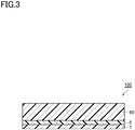
- Fig. 3 shows a device 100 which includes a transparent gas barrier film 1, a transparent conductive layer 5, and a driven unit 50.
- the device 100 may be electronic paper, an electrochromic device, an organic or inorganic electroluminescent device, or other organic semiconductor devices.
- the driven unit 50 is disposed so as to face the transparent gas barrier film 1 via the transparent conductive layer 5. The driven unit 50 is protected by the transparent gas barrier film 1 and driven via the transparent conductive layer 5.
- Fig. 4 is a set of schematic cross-sectional views in which (a) illustrates a second embodiment of the transparent conductive gas barrier laminate according to the present disclosure, and (b) illustrates a modification of the second embodiment.
- These figures respectively show laminates 20A and 20B each having a transparent gas barrier film 1 which includes two pairs of a transparent base film 1a and a barrier layer 1b, and an adhesive layer A1 interposed between the two pairs.
- the transparent gas barrier film 1 having such a configuration can contribute to achieving much better gas barrier properties.
- the two pairs are laminated so that the respective barrier layers 1b will face each other.
- a transparent conductive layer 5 is formed on a surface of the transparent base film 1a of one pair (upper pair as viewed in the figure).
- the two pairs are laminated so that the barrier layer 1b of one pair (lower pair as viewed in the figure) will face the transparent base film 1a of the other pair (upper pair as viewed in the figure).
- a transparent conductive layer 5 is formed on a surface of the barrier layer 1b of the upper pair.
- the adhesive layer A1 is formed of an adhesive or a tackifier.
- the adhesive may be an acrylic adhesive, an epoxy-based adhesive, a urethane-based adhesive, or the like.
- the tackifier may be an acrylic tackifier, a polyvinyl ether-based tackifier, a urethane-based tackifier, a silicone-based tackifier, or the like. Among them, an acrylic tackifier is particularly preferred because of having high transparency and good heat resistance.
- the adhesive layer A1 preferably has a thickness in the range of 0.5 ⁇ m to 50 ⁇ m, more preferably 1 ⁇ m to 20 ⁇ m, and even more preferably 2 ⁇ m to 6 ⁇ m.
- the adhesive that forms the adhesive layer A1 may be one having oxygen barrier properties.
- the adhesive layer A1 with a thickness of 5 ⁇ m may have an oxygen permeability, for example, of 1,000 cm 3 /(m 2 ⁇ day ⁇ atm) or less in the thickness direction.
- the oxygen permeability is preferably 500 cm 3 /(m 2 ⁇ day ⁇ atm) or less, more preferably 100 cm 3 /(m 2 ⁇ day ⁇ atm) or less, even more preferably 50 cm 3 /(m 2 ⁇ day ⁇ atm) or less, and particularly preferably 10 cm 3 /(m 2 ⁇ day ⁇ atm) or less.
- the adhesive layer A1 has an oxygen permeability of 1,000 cm 3 /(m 2 ⁇ day ⁇ atm) or less, the defects, if any, of the barrier layer 1b can be mitigated.
- the lower limit of the oxygen permeability is not particularly limited, but may, for example, be 0.1 cm 3 /(m 2 ⁇ day ⁇ atm).
- the adhesive layer A1 may preferably have ultraviolet shielding properties, from the perspective of preventing the conductive polymer contained in the transparent conductive layer 5 and/or the driven unit 50 from being deteriorated by ultraviolet rays. Specifically, it is preferred that the adhesive layer A1 contains an ultraviolet absorber.
- the ultraviolet absorber may be one that contains a benzotriazole-based compound, a benzophenone-based compound, or a triazine-based compound.
- a commercially available product Tinuvin (trademark) 400 manufactured by BASF SE may be used.
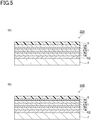
- Fig. 5 is a set of schematic cross-sectional views in which (a) illustrates a third embodiment of the transparent conductive gas barrier laminate according to the present disclosure, and (b) illustrates a modification of the third embodiment.
- These figures respectively show laminates 30A and 30B which are different from the laminates 20A and 20B described above in that the laminates 30A and 30B each include a transparent resin film 7 additionally adhered thereto via an adhesive layer A2.
- the adhesive layer A2 may adequately have a configuration similar to that of the adhesive layer A1 (in terms of type, thickness, oxygen barrier properties, and ultraviolet shielding properties).
- the transparent resin film 7 may preferably have a total light transmittance of 85% or more, although not particularly limited thereto.
- polyethylene terephthalate films, polyethylene naphthalate films, or the like having high transparency and good heat resistance may be used.
- Films having ultraviolet shielding properties may also be used as the transparent resin film 7.
- the transparent resin film 7 may have a thickness, for example, in the range of 10 ⁇ m to 250 ⁇ m, preferably 25 ⁇ m to 240 ⁇ m, more preferably 40 ⁇ m to 210 ⁇ m, and even more preferably 55 ⁇ m to 200 ⁇ m. If the transparent conductive layer 5 is patterned, instead of being a uniform coating, the transparent resin film 7 with a thickness of 10 ⁇ m or more can make the pattern not be easily visible from outside. If the thickness of the transparent resin film 7 is 250 ⁇ m or less, the total thickness of the laminate 30A or 30B is prevented from becoming excessively large.
- Fig. 6 is a set of schematic cross-sectional views in which (a) illustrates a fourth embodiment of the transparent conductive gas barrier laminate according to the present disclosure, and (b) illustrates a modification of the fourth embodiment.
- These figures respectively show laminates 40A and 40B which are different from the laminates 30A and 30B described above in that the laminates 40A and 40B each have a coating layer 9 that is additionally formed on the outer side of the transparent resin film 7.
- the coating layer 9 for example, one that contains a curing material and a leveling material as binder matrix components may be used.
- a coating layer 9 mainly formed of a curing material may allow the coating layer 9 to serve as a hard coating.
- the laminate 40A or 40B can have a surface strength corresponding to a pencil hardness of H or more (more preferably 2H or more).
- the coating layer 9 may be one that imparts stain resistance and/or chemical resistance to the outermost surface.
- a conductive material may be added to the coating layer 9 to impart antistatic properties thereto.
- the coating layer 9 may have a thickness, for example, in the range of 40 ⁇ m to 120 ⁇ m, preferably 50 ⁇ m to 100 ⁇ m, and more preferably 60 ⁇ m to 80 ⁇ m.
- the coating layer 9 having a thickness of 40 ⁇ m or more easily allows the coating layer 9 to sufficiently exert its performance, and makes the pattern, if any, of the transparent conductive layer 5 not easily visible from outside. If the coating layer 9 has a thickness of 120 ⁇ m or less, the total thickness of the laminate 40A or 40B is easily prevented from becoming excessively large.
- the present embodiment has exemplified a configuration in which the coating layer 9 is formed on the outside of the transparent resin film 7.
- the configuration may be such that the coating layer 9 is formed on the surface of the transparent base film 1a which is on the outside of the laminate 20A or 20B of the second embodiment.
- the adhesive layers A1 and A2 may have ultraviolet shielding properties.
- each transparent base film 1a may be one having ultraviolet shielding properties so that the ultraviolet shielding properties can be imparted to the transparent gas barrier film 1. By imparting ultraviolet shielding properties to the transparent gas barrier film 1, the transparent conductive layer 5 can be protected from ultraviolet rays and thus increase of sheet resistance over time can be minimized.
- the transparent conductive gas barrier laminates according to the embodiments described above can be produced, for example, by roll-to-roll processing.
- a transparent gas barrier film 1 is prepared. Specifically, a vapor-deposited layer 1v is laminated by vacuum deposition on a surface of a transparent base film 1a.
- a coating agent containing a main agent is prepared.
- the main agent is an aqueous solution or water/alcohol mixed solution that contains at least one component or the like selected from the group consisting of hydroxyl group-containing polymer compounds, metal alkoxides, hydrolyzed metal alkoxides, and polymerized metal alkoxides.
- the coating agent containing the main agent is applied to the surface of the vapor-deposited layer 1v, followed by drying at 80°C to 250°C, for example, thereby forming a gas barrier covering layer 1c.
- the obtained laminate film may be singly used as a transparent gas barrier film 1 (first embodiment), or may be bonded to another such laminate film via an adhesive layer A1 for use as a transparent gas barrier film 1.
- a transparent conductive layer 5 may be formed on the inner surface of the transparent gas barrier film 1, or, as necessary, a transparent film 7 may be bonded to the outer surface thereof via an adhesive layer A2, or a coating layer 9 may be further formed on the outside of the transparent resin film 7 to obtain a transparent conductive gas barrier laminate of an embodiment described above.
- tristimulus values X, Y and Z of the object color based on transmission in the tristimulus values XYZ color system were calculated from the following formulas to calculate b*.
- moisture permeability was measured under conditions of 40°C transmission cell temperature, 90% RH in a high humidity chamber, and 0% RH in a low humidity chamber.
- a transparent gas barrier film was prepared as follows. First, an acrylic resin coating liquid was applied to a surface of a PET film, as a transparent base film, having a thickness of 23 ⁇ m and dried to form an anchor coat layer. Then, silicon oxide was vacuum-deposited on the anchor coat layer so as to have a thickness of 30 nm to provide a vapor-deposited layer. Furthermore, a gas barrier covering layer having a thickness of 300 nm was formed on the vapor-deposited layer. The gas barrier covering layer was formed by a wet coating method by applying a coating liquid which contained tetraethoxysilane and polyvinyl alcohol. Thus, a transparent gas barrier film was obtained, with a barrier layer being provided on one surface of the transparent base film. The barrier layer in this case was formed of a pair of a silicon oxide-deposited layer and a gas barrier covering layer (see Fig. 2(a) ).
- a transparent conductive layer having a thickness of 400 nm was further formed to produce a transparent conductive gas barrier laminate (see Fig. 1(a) ).
- the transparent conductive layer was formed by a wet coating method by applying a coating liquid that contained PEDOT/PSS (manufactured by Nagase ChemteX Corporation).
- a transparent conductive gas barrier laminate was formed as in Example 1 except that a transparent conductive layer was formed on the other surface of the transparent base film, instead of forming a transparent conductive layer on the gas barrier covering layer (see Fig. 1(b) ).
- Example 2 Two transparent gas barrier films were prepared as in Example 1. The two transparent gas barrier films were bonded to each other such that the respective gas barrier covering layers face each other to thereby obtain a transparent gas barrier film having a multilayer structure. On a surface of the transparent barrier film (on a surface of the PET film) obtained as described above, a transparent conductive layer was formed as in Example 1 to produce a transparent conductive gas barrier laminate (see Fig. 4(a) ).
- an adhesive layer (oxygen permeability under 30°C 70% RH environment: 5 cm 3 /m 2 ⁇ day ⁇ atm) having a cured thickness of 5 ⁇ m was formed using a two-part epoxy adhesive comprising an epoxy resin as a base resin and an amine-based curing agent.
- Oxygen permeability of the adhesive layer was measured as follows. On an OPP film having a thickness of 20 ⁇ m (oxygen permeability under a 30°C and 70% RH environment: 3,000 cm 3 /m 2 ⁇ day ⁇ atm (measurement limit) or more), a film of the two-part epoxy adhesive was formed so as to have a cured thickness of 5 ⁇ m to thereby prepare an evaluation sample. Oxygen permeability of the sample was measured under a 30°C and 70% RH environment according to the method described in JIS K7126A by using a differential pressure gas meter (GTR-10X, manufactured by GTR Tec Corporation).
- a transparent gas barrier film having a multilayer structure was formed as in Example 3 except that two transparent gas barrier films were bonded to each other such that the gas barrier covering layer of one transparent gas barrier film faced the PET film of the other transparent gas barrier film, instead of bonding the two transparent gas barrier films such that the respective gas barrier covering layers faced each other.
- a transparent conductive layer was formed as in Example 1 to produce a transparent conductive gas barrier laminate (see Fig. 4(b) ).
- a transparent conductive gas barrier laminate was produced as in Example 3 except that a UV absorber (manufactured by BASF SE) was added to the adhesive used for bonding the two transparent barrier films (see Fig. 4(a) ).
- the amount of addition of the UV absorber was 1.5 parts by mass relative to the 100 parts by mass adhesive.
- a transparent conductive gas barrier laminate was produced as in Example 4 except that a UV absorber (manufactured by BASF SE) was added to the adhesive used for bonding the two transparent barrier films (see Fig. 4(b) ).
- the amount of addition of the UV absorber was 1.5 parts by mass relative to the 100 parts by mass adhesive.
- Transparent conductive gas barrier laminates were respectively produced as in Examples 3 to 6 except that transparent resin films were further bonded to the outer surfaces (PET films) of the respective laminates having the same configurations as those of the transparent conductive gas barrier laminates produced in Examples 3 to 6 (see Fig. 5(a) or 5(b) ).
- PET films each having a thickness of 50 ⁇ m, manufactured by Teijin DuPont Films
- ultraviolet shielding properties were used as the transparent resin films.
- the adhesive forming the adhesive layers an adhesive that was the same as that used in Example 3 was used.
- Transparent conductive gas barrier laminates were respectively produced as in Examples 9 and 10 except that the transparent resin films were bonded to the respective laminates via adhesive layers containing a UV absorber (see Fig. 5(a) or 5(b) ).
- a UV absorber see Fig. 5(a) or 5(b) .
- an adhesive that was the same as that used in Examples 5 and 6 was used.
- Transparent conductive gas barrier laminates were respectively produced as in Examples 7 to 12 except that coating layers, each having a thickness of 8 ⁇ m, were formed on the outer surfaces (surfaces of the respective transparent resin films) of the respective laminates having the same configurations as those of the transparent conductive gas barrier laminates produced in Examples 7 to 12 (see Fig. 6(a) or 6(b) ).
- the coating layers were formed by a wet coating method by applying a coating liquid that contained a photosensitive monomer and a photoinitiator, followed by curing by irradiating ultraviolet rays.
- the coating layers each had a pencil hardness of 2H.
- Example 3 A laminate having the same configuration as that of the transparent conductive gas barrier laminate (see Fig. 4(a) ) of Example 3 was produced as in Example 3 except that no transparent conductive layer was formed.
- Example 17 A laminate having the same configuration as that of the transparent conductive gas barrier laminate (see Fig. 6(a) ) of Example 17 was produced as in Example 17 except that no transparent conductive layer was formed.
- Transparent conductive gas barrier laminates were respectively produced as in Examples 1 to 18 except that barrier layers, each including two pairs of films, each pair being a silicon oxide-deposited layer and a gas barrier covering layer (see Fig. 2(b) ), were formed on the respective transparent base films, instead of forming barrier layers, each including one pair of a silicon oxide-deposited layer and a gas barrier covering layer, thereon.
- Laminates were respectively produced as in Comparative Examples 1 and 2 except that barrier layers, each including two pairs of films, each pair being a silicon oxide-deposited layer and a gas barrier covering layer (see Fig. 2(b) ), were formed on the respective transparent base films, instead of forming barrier layers, each including one pair of a silicon oxide-deposited layer and a gas barrier covering layer, thereon.
- Transparent conductive gas barrier laminates were respectively produced as in Examples 1 to 18 except that transparent base films (manufactured by Teijin Film Solutions Limited) having ultraviolet shielding properties were respectively used, instead of using transparent base films (PET films) not having ultraviolet shielding properties. It should be noted that the transparent gas barriers each had the same configuration as that shown in Fig. 2(a) .
- Transparent conductive gas barrier laminates were respectively produced as in Comparative Examples 1 and 2 except that transparent base films (manufactured by Teijin Film Solutions Limited) having ultraviolet shielding properties were respectively used, instead of using transparent base films (PET films) not having ultraviolet shielding properties. It should be noted that the transparent gas barriers each had the same configuration as that shown in Fig. 2(a) .
- Tables 1 to 3 collectively show configurations, evaluations and the like of the laminates related to the examples and the comparative examples set forth above.
- the item "b* value of transparent gas barrier film” of Examples 3 to 18 in Table 1, Examples 21 to 36 in Table 2, and Examples 39 to 54 in Table 3 is a b* value of a transparent gas barrier film having a multilayer structure obtained by bonding two transparent barrier films to each other.
- [Table 1] Configuration of laminate UV absorber in adhesive layer b* value of transparent gas barrier film b* value of entire laminate Total light transmittance [%] Moisture permeability [g/m 2 ⁇ day] Sheet resistance [ ⁇ / ⁇ ] Adhesive layer A1 Adhesive layer A2 Earlier stage After UV exposure Example 1 Fig.
- a transparent conductive gas barrier laminate in which a yellowish hue has been sufficiently reduced, and a device including the laminate.
Landscapes
- Chemical & Material Sciences (AREA)
- Organic Chemistry (AREA)
- Health & Medical Sciences (AREA)
- Chemical Kinetics & Catalysis (AREA)
- Medicinal Chemistry (AREA)
- Polymers & Plastics (AREA)
- Physics & Mathematics (AREA)
- Inorganic Chemistry (AREA)
- Nonlinear Science (AREA)
- General Physics & Mathematics (AREA)
- Optics & Photonics (AREA)
- Engineering & Computer Science (AREA)
- Materials Engineering (AREA)
- Laminated Bodies (AREA)
Abstract
Description
- The present disclosure relates to a transparent conductive gas barrier laminate including a transparent gas barrier film and a transparent conductive layer in this order from outside toward inside, and a device including the laminate.
- Electronic devices having a structure protected by a laminate film are under development. Such a laminate film includes a moisture-resistant layer or a gas barrier layer. For example,
PTL 1 discloses a support for a conductive layer which includes a resin sheet, a moisture-resistant layer, an adhesive layer and a resin sheet in this order, and electronic paper using the support. PTL 2 discloses a transparent conductive film including a base layer, a gas barrier layer made of a predetermined material, and a transparent conductive layer, and an electronic device including the film. -
- PTL 1:
JP 2003-175566 A - PTL 2:
JP 2012-86378 A - Transparent gas barrier laminates used for electronic devices are not necessarily colorless and transparent but may have a hue although they may yet be transparent, depending on the materials of the layers or films included in the laminate, or the conditions for forming the layers or films. In particular, transparent gas barrier laminates based on the conventional art tend to have a yellowish hue as stated below.
- As a material for forming conventional transparent conductive layers, indium tin oxide (ITO) has been widely used. Transparent conductive layers made of ITO are formed, for example, by sputtering on a transparent resin film. When a transparent conductive layer of ITO is formed on a transparent resin film under temperature conditions not thermally deteriorating the transparent resin film (e.g., about 150°C), the ITO contained in the layer may be amorphous. Such amorphous ITO has low transmissivity for short-wavelength light, such as blue light. Therefore, the transparent conductive layer may appear to have a yellowish hue.
- As layers serving as a gas barrier in a transparent gas barrier laminate, vapor-deposited layers made of silicon oxide have been used. According to research conducted by the inventors of the present invention, vapor-deposited layers obtained by depositing silicon oxide may also appear to have a yellowish hue, depending on the temperature conditions or the like.
- Device makers or consumers in recent years tend to avoid transparent materials having a yellowish hue. To cope with this, the present disclosure aims to provide a transparent conductive gas barrier laminate in which a yellowish hue has been sufficiently reduced, and a device including the laminate.
- An aspect of the present disclosure relates to a transparent conductive gas barrier laminate including a transparent gas barrier film and a transparent conductive layer in this order from outside toward inside. In the transparent conductive gas barrier laminate, the transparent gas barrier film has a b* value of more than 0 in the L*a*b* color system, and the transparent conductive layer contains a conductive polymer and has a b* value of less than 0 in the L*a*b* color system. The expression "b* of more than 0 in the L*a*b* color system" refers to having a yellowish hue, while the expression "b* of less than 0 in the L*a*b* color system" refers to having a bluish hue. The term "inside" of the transparent conductive gas barrier laminate refers to a side on which a driven unit to be protected by the laminate is disposed, and the term "outside" refers to a side facing away from the inside. The term "transparent" refers to being transparent at least for visible light.
- In the transparent conductive gas barrier laminate, the transparent gas barrier film having a yellowish hue is combined with the transparent conductive layer having a bluish hue. Yellow and blue are in a complementary relationship. Therefore, even though the transparent gas barrier film has a yellowish hue, the transparent conductive layer having a bluish hue exerts an overall effect of reducing the yellowish hue when the transparent conductive gas barrier laminate is observed.
- An example of the transparent gas barrier film having a yellowish hue may be one that includes a transparent base film and a barrier layer which is formed on at least one surface of the transparent base film. A specific example of the barrier layer may be one which at least includes a silicon oxide-deposited layer. As mentioned above, a silicon oxide-deposited layer tends to have a yellowish hue. If the silicon oxide-deposited layer having a yellowish hue is combined with the transparent conductive layer having a bluish hue, the yellowish hue is reduced overall when the transparent conductive gas barrier laminate is observed. From the perspective of achieving high gas barrier properties, the transparent gas barrier film may include at least two pairs of films, each pair being a transparent base film and a barrier layer, with an adhesive layer interposed therebetween, and each barrier layer in this case may at least include a silicon oxide-deposited layer.
- The material for forming the transparent conductive layer having a bluish hue may be a conductive polymer which contains a mixture of polyethylene dioxythiophene (PEDOT) and polystyrene sulfonic acid (PPS) (this mixture may be termed PEDOT/PSS hereinafter). Specifically, the transparent conductive gas barrier laminate according to the present disclosure includes a transparent gas barrier film and a transparent conductive layer in this order from outside toward inside. In the laminate, the transparent gas barrier film has a b* value of more than 0 in the L*a*b* color system, and the transparent conductive layer contains PEDOT/PSS and has a b* value of less than 0 in the L*a*b* color system. Even though the transparent gas barrier film has a yellowish hue, the transparent conductive layer, which contains PEDOT/PSS having a bluish hue, may exert an overall effect of reducing the yellowish hue when the transparent conductive gas barrier laminate is observed and may even exert an effect of imparting a bluish hue to the laminate.
- ITO films based on conventional art for use as transparent conductive films tend to have a yellowish hue as mentioned above. ITO films tend to cause fine cracks as a result of repeating input operations, and also suffer from low bending resistance. In addition to this, formation of ITO films involves vacuum processing, such as deposition or sputtering, which incurs enormous capital investment and needs a large site area that is difficult to obtain. Furthermore, indium, which is a rare metal, suffers from depletion of resources and generates a concern that stable supply may be affected by the international situation. In this regard, use of PEDOT/PSS as a material for forming a transparent conductive layer can eliminate these issues. PEDOT/PSS has good electrical conductivity, flexibility and transparency. Transparent conductive layers containing PEDOT/PSS can be applied by using a wet coating method and thus are superior to ITO films from the perspective of cost.
- PEDOT/PSS, which is an organic material, has lower resistance to ultraviolet rays (with a wavelength of 300 nm to 400 nm) compared to inorganic materials. Therefore, if devices including the transparent conductive gas barrier laminate are used under environments of being exposed to ultraviolet (UV) rays or used in fields requiring high reliability, the laminate may preferably have ultraviolet shielding properties. When ultraviolet shielding properties are imparted to the transparent conductive gas barrier laminate, deterioration may be minimized in the driven unit to be protected by the laminate.
- For example, ultraviolet shielding properties may be imparted to the transparent conductive gas barrier laminate by using a transparent gas barrier film having ultraviolet shielding properties. More specifically, the laminate may include a transparent base film having ultraviolet shielding properties, or may include a layer having ultraviolet shielding properties (e.g., layer containing a UV absorber), as the adhesive layer, interposed between two pairs of films, each pair being a transparent base film and a silicon oxide-deposited film. Alternatively, the transparent conductive gas barrier laminate may further include a transparent resin film having ultraviolet shielding properties on the outside of the transparent conductive layer, or may include a layer having ultraviolet shielding properties (e.g., layer containing a UV absorber), as the adhesive layer, interposed between the transparent resin film having ultraviolet shielding properties and a film adjacent to the transparent resin film.
- The transparent conductive gas barrier laminate may further include a coating layer on the outermost side thereof. For example, by forming a coating layer having a pencil hardness of 2H or more, crack resistance can be imparted to the outermost surface. The coating layer may be one that imparts stain resistance and/or chemical resistance to the outermost surface.
- An aspect of the present disclosure is a device including the transparent conductive gas barrier laminate described above, and a driven unit that is disposed so as to face the transparent conductive layer of the transparent conductive gas barrier laminate. The driven unit of this device is protected by the transparent gas barrier film and driven via the transparent conductive layer.
- According to the present disclosure, there are provided a transparent conductive gas barrier laminate in which a yellowish hue has been sufficiently reduced, and a device including the laminate.
-
-
Fig. 1 is a set of schematic cross-sectional views in which (a) illustrates a first embodiment of a transparent conductive gas barrier laminate according to the present disclosure, and (b) illustrates a modification of the first embodiment. -
Fig. 2 is a set of schematic cross-sectional views in which (a) illustrates an example of a configuration of a transparent gas barrier film, and (b) illustrates another example of a configuration of a transparent gas barrier film. -
Fig. 3 is a schematic cross-sectional view illustrating an embodiment of a device including a transparent conductive gas barrier laminate. -
Fig. 4 is a set of schematic cross-sectional views in which (a) illustrates a second embodiment of the transparent conductive gas barrier laminate according to the present disclosure, and (b) illustrates a modification of the second embodiment. -
Fig. 5 is a set of schematic cross-sectional views in which (a) illustrates a third embodiment of the transparent conductive gas barrier laminate according to the present disclosure, and (b) illustrates a modification of the third embodiment. -
Fig. 6 is a set of schematic cross-sectional views in which (a) illustrates a fourth embodiment of the transparent conductive gas barrier laminate according to the present disclosure, and (b) illustrates a modification of the fourth embodiment. - With reference to the drawings, some embodiments of the present disclosure will be described in detail. It should be noted that, in the drawings, like or corresponding parts are designated with like reference signs to avoid duplicate description. Also, when terms related to positions, such as left, right, upper and lower, are mentioned, they are the positions as viewed in the figures, unless otherwise stated. Furthermore, scales are not limited to those shown in the drawings.
-
Fig. 1(a) illustrates a transparent conductive gas barrier laminate (which may be simply termed "laminate" hereinafter) 10A which includes a transparentgas barrier film 1 and a transparentconductive layer 5 in this order from outside (lower side in the figure) toward inside (upper side in the figure) of the laminate. As shown inFig. 1(a) , the transparentgas barrier film 1 in thelaminate 10A is configured by atransparent base film 1a and abarrier layer 1b which are laminated in this order from outside toward inside. The order of lamination is not limited to this but may be the order as in the configuration of a laminate 10B shown inFig. 1(b) . The laminate 10B has a layer configuration in which abarrier layer 1b is formed on a surface of atransparent base film 1a, and a transparentconductive layer 5 is formed on the other surface thereof. - The transparent
gas barrier film 1 has a b* value of more than 0 in the L*a*b* color system. The transparentconductive layer 5 contains a conductive polymer, and has a b* value of less than 0 in the L*a*b* color system. By combining the transparentgas barrier film 1 having a yellowish hue with the transparentconductive layer 5 having a bluish hue, the yellowish hue of the transparentgas barrier film 1 is reduced by the bluish hue of the transparentconductive layer 5. In other words, in the obtainedlaminate - The transparent
gas barrier film 1 may have b* of more than 0 in the L*a*b* color system (i.e. may have a yellowish hue). The transparentgas barrier film 1 may have a configuration including thetransparent base film 1a and thebarrier layer 1b which is formed on a surface of thetransparent base film 1a. The transparentgas barrier film 1 may have a yellowish hue that is ascribable to one or both of thetransparent base film 1a and thebarrier layer 1b. However, since a sufficiently colorless and transparent film is comparatively easily available as thetransparent base film 1a, the yellowish hue of the transparentgas barrier film 1 is assumed to be ascribable to thebarrier layer 1b. - The transparent
gas barrier film 1 may have b* of more than 0, or more than 0 and 2.5 or less, or may have b* in the range of 0.5 to 2.0, or 0.5 to 1.5. If the transparentgas barrier film 1 has a b* value of 2.5 or less, the yellowish hue of the transparent conductivegas barrier laminate 10A can be sufficiently reduced by the bluish hue of the transparentconductive layer 5. - It is preferred that a sufficiently colorless and transparent film is used as the
transparent base film 1a. Thetransparent base film 1a preferably has a total light transmittance of 85% or more. As thetransparent base film 1a, for example, a film having high transparency and good heat resistance may be used. Such a film may be a polyethylene terephthalate film (PET film), a polyethylene naphthalate film, or the like. Thetransparent base film 1a may preferably have a thickness in the range of 9 µm to 50 µm, and more preferably 12 µm to 30 µm. If thetransparent base film 1a has a thickness of 9 µm or more, the strength of thetransparent base film 1a can be sufficiently ensured, and if 50 µm or less, a long roll (roll of the transparent gas barrier film 1) can be produced efficiently and economically. - As shown in
Fig. 2(a) , for example, thebarrier layer 1b is configured by a vapor-depositedlayer 1v and a gasbarrier covering layer 1c. Specifically, thebarrier layer 1b has a configuration in which a vapor-depositedlayer 1v is provided on a surface of atransparent resin film 1a, and a gasbarrier covering layer 1c is provided on the vapor-depositedlayer 1v. As shown inFig. 2(b) , for example, thebarrier layer 1b may be configured by an alternation of vapor-depositedlayers 1v and gas barrier coating layers 1c. Although not shown,barrier layers 1b may be respectively formed on both surfaces of atransparent base film 1a. To improve adhesion between thetransparent base film 1a and the vapor-depositedlayer 1v, the surface of thetransparent base film 1a may be treated, e.g., plasma-treated, or may be provided with an acrylic resin layer, an anchor coat layer made of a polyester resin, a urethane resin, or the like. - The vapor-deposited
layer 1v may be formed, for example, by vapor-depositing aluminum oxide, silicon oxide, silicon oxynitride, magnesium oxide, or a mixture thereof on thetransparent base film 1a. Of these inorganic materials, aluminum oxide or silicon oxide is preferably used from the perspective of barrier properties and productivity. The vapor-deposited layer is formed by vacuum vapor deposition, sputtering, CVD, or the like. As described above, according to the research conducted by the inventors of the present invention, if a vapor-deposited layer of silicon oxide is formed, for example, by vacuum vapor deposition, the resultantly obtained vapor-depositedlayer 1v is likely to have a yellowish hue. - The vapor-deposited
layer 1v preferably has a thickness (film thickness) in the range of 5 nm to 500 nm, and more preferably 10 nm to 100 nm. If the film thickness is 5 nm or more, a uniform film is easily formed, and the film is likely to more sufficiently serve as a gas barrier member. If the film thickness is 500 nm or less, there is a tendency that sufficient flexibility can be maintained, and that the resultant thin film is more reliably prevented from being cracked due to external factors, such as bending or stretching, after being formed. - The gas
barrier covering layer 1c is provided for the purpose of preventing various types of secondary damage in the post processing and imparting higher barrier properties to the laminate. From the perspective of obtaining good barrier properties, the gasbarrier covering layer 1c preferably contains at least one component selected from the group consisting of hydroxyl group-containing polymer compound, metal alkoxide, metal alkoxide hydrolysate and metal alkoxide polymer. - Specific examples of the hydroxyl group-containing polymer compound include water-soluble polymers, such as polyvinyl alcohol, polyvinyl pyrrolidone, and starch. Particularly, the best barrier properties are obtained when polyvinyl alcohol is used.
- The metal alkoxide is a compound represented by a general formula: M(OR)n (where M represents a metal atom such as Si, Ti, A1 or Zr, R represents an alkyl group such as -CH3 or -C2H5, and n represents an integer corresponding to a valence of M). Specifically, such a compound may be tetraethoxysilane [Si(OC2H5)4], triisopropoxy aluminum [Al(O-iso-C3H7)3], or the like. Tetraethoxysilane or triisopropoxy aluminum is preferred because they are relatively stable in an aqueous solvent after being hydrolyzed. The hydrolyzed or polymerized metal alkoxide may, for example, be silicic acid (Si(OH)4) as hydrolyzed or polymerized tetraethoxysilane, or aluminum hydroxide (Al(OH)3) as hydrolyzed or polymerized tripropoxy aluminum.
- The gas
barrier covering layer 1c preferably has a thickness (film thickness) in the range of 50 nm to 1,000 nm, and more preferably 100 nm to 500 nm. If the film thickness is 50 nm or more, more sufficient gas barrier properties are likely to be obtained, and if 1,000 nm or less, sufficient flexibility is likely to be maintained. - The transparent
conductive layer 5, which contains a conductive polymer, has electrical conductivity and has a bluish hue. The transparentconductive layer 5 may have b* of less than 0 (i.e. may have a negative value), preferably less than 0 and -5.0 or more, more preferably in the range of -1.0 to -3.0, and even more preferably -1.0 to -2.0. If the transparentconductive layer 5 has a b* value of less than -5.0, the bluish color may tend to allow thelaminate laminate conductive layer 5 may preferably have b* whose absolute value is larger than that of the b* of the transparentgas barrier film 1. Specifically, the ratio of the absolute value of b* of the transparent conductive layer 5 (B5) to the value of b* of the transparent gas barrier film 1 (B1) as expressed by (B5/B1) is preferably more than 1, and more preferably in the range of 2.0 to 4.0. - The transparent
conductive layer 5 preferably has a thickness (film thickness) in the range of 0.1 µm to 2.0 µm, and more preferably 0.1 µm to 0.4 µm. If the film thickness is 0.1 µm or more, a uniform film is easily formed, and the film is likely to more sufficiently serve as a conductive layer. If the film thickness is 2.0 µm or less, there is a tendency that sufficient flexibility can be maintained, and that the resultant thin film is more reliably prevented from being cracked due to external factors, such as bending or stretching, after being formed. For example, the transparentconductive layer 5 may have a sheet resistance in the range of 100 Ω/□ to 1,000 Ω/□, preferably 100 Ω/□ to 500 Ω/□, and more preferably 100 Ω/□ to 150 Ω/□. The sheet resistance of the transparentconductive layer 5 can be measured, for example, by using a Loresta-GP MCP-T610 (trade name, manufactured by Mitsubishi Chemical Analytech Co.,Ltd.). - The transparent
conductive layer 5 can be formed, for example, by applying a coating liquid that contains a conductive polymer having a bluish hue. As a specific example of the conductive polymer having a bluish hue, a mixture of polyethylene dioxythiophene (PEDOT) and polystyrene sulfonic acid (PPS) (PEDOT/PSS) may be mentioned. The degree of blue of the transparentconductive layer 5 may be controlled, for example, by controlling the thickness of the transparentconductive layer 5, or controlling the polymerization degree of the conductive polymer. If the material forming the transparentconductive layer 5 is colorless and transparent or has insufficient degree of blue, a blue pigment or the like may be added to the coating liquid to an extent not hampering electrical conductivity. The transparentconductive layer 5 may be formed so as to entirely cover the transparent gas barrier film 1 (so-called solid coating), or may be formed into a pattern. -
Fig. 3 shows adevice 100 which includes a transparentgas barrier film 1, a transparentconductive layer 5, and a drivenunit 50. Specifically, for example, thedevice 100 may be electronic paper, an electrochromic device, an organic or inorganic electroluminescent device, or other organic semiconductor devices. As shown inFig. 3 , the drivenunit 50 is disposed so as to face the transparentgas barrier film 1 via the transparentconductive layer 5. The drivenunit 50 is protected by the transparentgas barrier film 1 and driven via the transparentconductive layer 5. -
Fig. 4 is a set of schematic cross-sectional views in which (a) illustrates a second embodiment of the transparent conductive gas barrier laminate according to the present disclosure, and (b) illustrates a modification of the second embodiment. These figures respectively showlaminates gas barrier film 1 which includes two pairs of atransparent base film 1a and abarrier layer 1b, and an adhesive layer A1 interposed between the two pairs. The transparentgas barrier film 1 having such a configuration can contribute to achieving much better gas barrier properties. - In the
laminate 20A shown inFig. 4(a) , the two pairs are laminated so that therespective barrier layers 1b will face each other. A transparentconductive layer 5 is formed on a surface of thetransparent base film 1a of one pair (upper pair as viewed in the figure). In the laminate 20B shown inFig. 4(b) , the two pairs are laminated so that thebarrier layer 1b of one pair (lower pair as viewed in the figure) will face thetransparent base film 1a of the other pair (upper pair as viewed in the figure). A transparentconductive layer 5 is formed on a surface of thebarrier layer 1b of the upper pair. - The adhesive layer A1 is formed of an adhesive or a tackifier. The adhesive may be an acrylic adhesive, an epoxy-based adhesive, a urethane-based adhesive, or the like. The tackifier may be an acrylic tackifier, a polyvinyl ether-based tackifier, a urethane-based tackifier, a silicone-based tackifier, or the like. Among them, an acrylic tackifier is particularly preferred because of having high transparency and good heat resistance. The adhesive layer A1 preferably has a thickness in the range of 0.5 µm to 50 µm, more preferably 1 µm to 20 µm, and even more preferably 2 µm to 6 µm.
- The adhesive that forms the adhesive layer A1 may be one having oxygen barrier properties. In this case, the adhesive layer A1 with a thickness of 5 µm may have an oxygen permeability, for example, of 1,000 cm3/(m2·day·atm) or less in the thickness direction. The oxygen permeability is preferably 500 cm3/(m2·day·atm) or less, more preferably 100 cm3/(m2·day·atm) or less, even more preferably 50 cm3/(m2·day·atm) or less, and particularly preferably 10 cm3/(m2·day·atm) or less. If the adhesive layer A1 has an oxygen permeability of 1,000 cm3/(m2·day·atm) or less, the defects, if any, of the
barrier layer 1b can be mitigated. The lower limit of the oxygen permeability is not particularly limited, but may, for example, be 0.1 cm3/(m2·day·atm). - The adhesive layer A1 may preferably have ultraviolet shielding properties, from the perspective of preventing the conductive polymer contained in the transparent
conductive layer 5 and/or the drivenunit 50 from being deteriorated by ultraviolet rays. Specifically, it is preferred that the adhesive layer A1 contains an ultraviolet absorber. The ultraviolet absorber may be one that contains a benzotriazole-based compound, a benzophenone-based compound, or a triazine-based compound. A commercially available product Tinuvin (trademark) 400 (manufactured by BASF SE) may be used. -
Fig. 5 is a set of schematic cross-sectional views in which (a) illustrates a third embodiment of the transparent conductive gas barrier laminate according to the present disclosure, and (b) illustrates a modification of the third embodiment. These figures respectively showlaminates laminates laminates transparent resin film 7 additionally adhered thereto via an adhesive layer A2. As necessary, the adhesive layer A2 may adequately have a configuration similar to that of the adhesive layer A1 (in terms of type, thickness, oxygen barrier properties, and ultraviolet shielding properties). - The
transparent resin film 7 may preferably have a total light transmittance of 85% or more, although not particularly limited thereto. For example, polyethylene terephthalate films, polyethylene naphthalate films, or the like having high transparency and good heat resistance may be used. Films having ultraviolet shielding properties may also be used as thetransparent resin film 7. - The
transparent resin film 7 may have a thickness, for example, in the range of 10 µm to 250 µm, preferably 25 µm to 240 µm, more preferably 40 µm to 210 µm, and even more preferably 55 µm to 200 µm. If the transparentconductive layer 5 is patterned, instead of being a uniform coating, thetransparent resin film 7 with a thickness of 10 µm or more can make the pattern not be easily visible from outside. If the thickness of thetransparent resin film 7 is 250 µm or less, the total thickness of the laminate 30A or 30B is prevented from becoming excessively large. -
Fig. 6 is a set of schematic cross-sectional views in which (a) illustrates a fourth embodiment of the transparent conductive gas barrier laminate according to the present disclosure, and (b) illustrates a modification of the fourth embodiment. These figures respectively showlaminates laminates laminates coating layer 9 that is additionally formed on the outer side of thetransparent resin film 7. - As the
coating layer 9, for example, one that contains a curing material and a leveling material as binder matrix components may be used. Use of acoating layer 9 mainly formed of a curing material may allow thecoating layer 9 to serve as a hard coating. Thus, thelaminate coating layer 9 may be one that imparts stain resistance and/or chemical resistance to the outermost surface. A conductive material may be added to thecoating layer 9 to impart antistatic properties thereto. - The
coating layer 9 may have a thickness, for example, in the range of 40 µm to 120 µm, preferably 50 µm to 100 µm, and more preferably 60 µm to 80 µm. Thecoating layer 9 having a thickness of 40 µm or more easily allows thecoating layer 9 to sufficiently exert its performance, and makes the pattern, if any, of the transparentconductive layer 5 not easily visible from outside. If thecoating layer 9 has a thickness of 120 µm or less, the total thickness of the laminate 40A or 40B is easily prevented from becoming excessively large. - The present embodiment has exemplified a configuration in which the
coating layer 9 is formed on the outside of thetransparent resin film 7. However, the configuration may be such that thecoating layer 9 is formed on the surface of thetransparent base film 1a which is on the outside of the laminate 20A or 20B of the second embodiment. Also, the present embodiment has described that the adhesive layers A1 and A2 may have ultraviolet shielding properties. However, for example, eachtransparent base film 1a may be one having ultraviolet shielding properties so that the ultraviolet shielding properties can be imparted to the transparentgas barrier film 1. By imparting ultraviolet shielding properties to the transparentgas barrier film 1, the transparentconductive layer 5 can be protected from ultraviolet rays and thus increase of sheet resistance over time can be minimized. - The transparent conductive gas barrier laminates according to the embodiments described above can be produced, for example, by roll-to-roll processing. First, a transparent
gas barrier film 1 is prepared. Specifically, a vapor-depositedlayer 1v is laminated by vacuum deposition on a surface of atransparent base film 1a. Subsequently, a coating agent containing a main agent is prepared. The main agent is an aqueous solution or water/alcohol mixed solution that contains at least one component or the like selected from the group consisting of hydroxyl group-containing polymer compounds, metal alkoxides, hydrolyzed metal alkoxides, and polymerized metal alkoxides. The coating agent containing the main agent is applied to the surface of the vapor-depositedlayer 1v, followed by drying at 80°C to 250°C, for example, thereby forming a gasbarrier covering layer 1c. The obtained laminate film may be singly used as a transparent gas barrier film 1 (first embodiment), or may be bonded to another such laminate film via an adhesive layer A1 for use as a transparentgas barrier film 1. - A transparent
conductive layer 5 may be formed on the inner surface of the transparentgas barrier film 1, or, as necessary, atransparent film 7 may be bonded to the outer surface thereof via an adhesive layer A2, or acoating layer 9 may be further formed on the outside of thetransparent resin film 7 to obtain a transparent conductive gas barrier laminate of an embodiment described above. - Some embodiments of the present disclosure have so far been specifically described. However, the technical scope of the present invention should not be limited to these embodiments, but may be modified variously without departing from the spirit of the present invention.
- The present invention will be more specifically described below based on Examples and Comparative Examples; however, the present invention should not be limited to the following Examples. In Examples and Comparative Examples, b* in the L*a*b* color system, total light transmittance, moisture permeability, and sheet resistance were measured as follows.
- Using UV-2450 (trade name, manufactured by Shimadzu Corporation), spectral transmittance of a target film was measured. From the results of measurement, tristimulus values X, Y and Z of the object color based on transmission in the tristimulus values XYZ color system were calculated from the following formulas to calculate b*.

- Based on a method of measurement according to JIS K 7361-1 (ISO13468-1) and using a haze meter (trade name: HM-150 manufactured by Murakami Color Research Laboratory Co., Ltd.), total light transmittance was measured.
- Based on an infrared sensor method according to JIS K 7129 and using a moisture permeability measuring device (trade name: Permatran, manufactured by MOCON Inc.), moisture permeability was measured under conditions of 40°C transmission cell temperature, 90% RH in a high humidity chamber, and 0% RH in a low humidity chamber.
- Using a Loresta-GP MCP-T610 (trade name, manufactured by Mitsubishi Chemical Analytech Co.,Ltd.), sheet resistances (early stage and after UV exposure) of the transparent conductive layer were measured. Ultraviolet rays were irradiated from the transparent gas barrier film side toward the transparent conductive layer for 2,000 hours.
- A transparent gas barrier film was prepared as follows. First, an acrylic resin coating liquid was applied to a surface of a PET film, as a transparent base film, having a thickness of 23 µm and dried to form an anchor coat layer. Then, silicon oxide was vacuum-deposited on the anchor coat layer so as to have a thickness of 30 nm to provide a vapor-deposited layer. Furthermore, a gas barrier covering layer having a thickness of 300 nm was formed on the vapor-deposited layer. The gas barrier covering layer was formed by a wet coating method by applying a coating liquid which contained tetraethoxysilane and polyvinyl alcohol. Thus, a transparent gas barrier film was obtained, with a barrier layer being provided on one surface of the transparent base film. The barrier layer in this case was formed of a pair of a silicon oxide-deposited layer and a gas barrier covering layer (see
Fig. 2(a) ). - On the gas barrier covering layer of the transparent gas barrier film obtained as described above, a transparent conductive layer having a thickness of 400 nm was further formed to produce a transparent conductive gas barrier laminate (see
Fig. 1(a) ). The transparent conductive layer was formed by a wet coating method by applying a coating liquid that contained PEDOT/PSS (manufactured by Nagase ChemteX Corporation). The transparent conductive layer had a sheet resistance of 150 Ω/□. It should be noted that, on a surface of a transparent film (b*=0), only a transparent conductive layer having a thickness of 400 nm was formed in a manner similar to the present example to produce a laminate formed of the transparent film and the transparent conductive layer. - A transparent conductive gas barrier laminate was formed as in Example 1 except that a transparent conductive layer was formed on the other surface of the transparent base film, instead of forming a transparent conductive layer on the gas barrier covering layer (see
Fig. 1(b) ). - Two transparent gas barrier films were prepared as in Example 1. The two transparent gas barrier films were bonded to each other such that the respective gas barrier covering layers face each other to thereby obtain a transparent gas barrier film having a multilayer structure. On a surface of the transparent barrier film (on a surface of the PET film) obtained as described above, a transparent conductive layer was formed as in Example 1 to produce a transparent conductive gas barrier laminate (see
Fig. 4(a) ). - For bonding the two transparent barrier films, an adhesive layer (oxygen permeability under 30°C 70% RH environment: 5 cm3/m2·day·atm) having a cured thickness of 5 µm was formed using a two-part epoxy adhesive comprising an epoxy resin as a base resin and an amine-based curing agent. Oxygen permeability of the adhesive layer was measured as follows. On an OPP film having a thickness of 20 µm (oxygen permeability under a 30°C and 70% RH environment: 3,000 cm3/m2·day·atm (measurement limit) or more), a film of the two-part epoxy adhesive was formed so as to have a cured thickness of 5 µm to thereby prepare an evaluation sample. Oxygen permeability of the sample was measured under a 30°C and 70% RH environment according to the method described in JIS K7126A by using a differential pressure gas meter (GTR-10X, manufactured by GTR Tec Corporation).
- A transparent gas barrier film having a multilayer structure was formed as in Example 3 except that two transparent gas barrier films were bonded to each other such that the gas barrier covering layer of one transparent gas barrier film faced the PET film of the other transparent gas barrier film, instead of bonding the two transparent gas barrier films such that the respective gas barrier covering layers faced each other. On a surface of the transparent gas barrier film (on a surface of the gas barrier covering layer) obtained as described above, a transparent conductive layer was formed as in Example 1 to produce a transparent conductive gas barrier laminate (see
Fig. 4(b) ). - A transparent conductive gas barrier laminate was produced as in Example 3 except that a UV absorber (manufactured by BASF SE) was added to the adhesive used for bonding the two transparent barrier films (see
Fig. 4(a) ). The amount of addition of the UV absorber was 1.5 parts by mass relative to the 100 parts by mass adhesive. - A transparent conductive gas barrier laminate was produced as in Example 4 except that a UV absorber (manufactured by BASF SE) was added to the adhesive used for bonding the two transparent barrier films (see
Fig. 4(b) ). The amount of addition of the UV absorber was 1.5 parts by mass relative to the 100 parts by mass adhesive. - Transparent conductive gas barrier laminates were respectively produced as in Examples 3 to 6 except that transparent resin films were further bonded to the outer surfaces (PET films) of the respective laminates having the same configurations as those of the transparent conductive gas barrier laminates produced in Examples 3 to 6 (see
Fig. 5(a) or 5(b) ). PET films (each having a thickness of 50 µm, manufactured by Teijin DuPont Films) having ultraviolet shielding properties were used as the transparent resin films. As the adhesive forming the adhesive layers, an adhesive that was the same as that used in Example 3 was used. - Transparent conductive gas barrier laminates were respectively produced as in Examples 9 and 10 except that the transparent resin films were bonded to the respective laminates via adhesive layers containing a UV absorber (see
Fig. 5(a) or 5(b) ). As the adhesive forming the adhesive layers, an adhesive that was the same as that used in Examples 5 and 6 was used. - Transparent conductive gas barrier laminates were respectively produced as in Examples 7 to 12 except that coating layers, each having a thickness of 8 µm, were formed on the outer surfaces (surfaces of the respective transparent resin films) of the respective laminates having the same configurations as those of the transparent conductive gas barrier laminates produced in Examples 7 to 12 (see
Fig. 6(a) or 6(b) ). The coating layers were formed by a wet coating method by applying a coating liquid that contained a photosensitive monomer and a photoinitiator, followed by curing by irradiating ultraviolet rays. The coating layers each had a pencil hardness of 2H. - A laminate having the same configuration as that of the transparent conductive gas barrier laminate (see
Fig. 4(a) ) of Example 3 was produced as in Example 3 except that no transparent conductive layer was formed. - A laminate having the same configuration as that of the transparent conductive gas barrier laminate (see
Fig. 6(a) ) of Example 17 was produced as in Example 17 except that no transparent conductive layer was formed. - Transparent conductive gas barrier laminates were respectively produced as in Examples 1 to 18 except that barrier layers, each including two pairs of films, each pair being a silicon oxide-deposited layer and a gas barrier covering layer (see
Fig. 2(b) ), were formed on the respective transparent base films, instead of forming barrier layers, each including one pair of a silicon oxide-deposited layer and a gas barrier covering layer, thereon. - Laminates were respectively produced as in Comparative Examples 1 and 2 except that barrier layers, each including two pairs of films, each pair being a silicon oxide-deposited layer and a gas barrier covering layer (see
Fig. 2(b) ), were formed on the respective transparent base films, instead of forming barrier layers, each including one pair of a silicon oxide-deposited layer and a gas barrier covering layer, thereon. - Transparent conductive gas barrier laminates were respectively produced as in Examples 1 to 18 except that transparent base films (manufactured by Teijin Film Solutions Limited) having ultraviolet shielding properties were respectively used, instead of using transparent base films (PET films) not having ultraviolet shielding properties. It should be noted that the transparent gas barriers each had the same configuration as that shown in
Fig. 2(a) . - Transparent conductive gas barrier laminates were respectively produced as in Comparative Examples 1 and 2 except that transparent base films (manufactured by Teijin Film Solutions Limited) having ultraviolet shielding properties were respectively used, instead of using transparent base films (PET films) not having ultraviolet shielding properties. It should be noted that the transparent gas barriers each had the same configuration as that shown in
Fig. 2(a) . - Tables 1 to 3 collectively show configurations, evaluations and the like of the laminates related to the examples and the comparative examples set forth above. It should be noted that the item "b* value of transparent gas barrier film" of Examples 3 to 18 in Table 1, Examples 21 to 36 in Table 2, and Examples 39 to 54 in Table 3 is a b* value of a transparent gas barrier film having a multilayer structure obtained by bonding two transparent barrier films to each other.
[Table 1] Configuration of laminate UV absorber in adhesive layer b* value of transparent gas barrier film b* value of entire laminate Total light transmittance [%] Moisture permeability [g/m2· day] Sheet resistance [Ω/□] Adhesive layer A1 Adhesive layer A2 Earlier stage After UV exposure Example 1 Fig. 1(a) - - 0.29 -1.91 81.2 500×10-3 551 606 Example 2 Fig. 1(b) - - 0.37 -1.83 80.9 500×10-3 779 857 Example 3 Fig. 4(a) Absent - 0.67 -1.53 79.6 3×10⁻³ 312 346 Example 4 Fig. 4(b) Absent - 0.65 -1.55 78.8 4×10⁻³ 300 342 Example 5 Fig. 4(a) Present - 0.69 -1.51 78.1 3×10⁻³ 210 235 Example 6 Fig. 4(b) Present - 0.71 -1.49 78.2 3×10⁻³ 198 208 Example 7 Fig. 5(a) Absent Absent 0.76 -1.46 79.6 3×10⁻³ 299 311 Example 8 Fig. 5(b) Absent Absent 0.85 -1.36 78.8 5×10⁻³ 294 350 Example 9 Fig. 5(a) Present Absent 0.65 -1.55 78.1 3×10⁻³ 196 225 Example 10 Fig. 5(b) Present Absent 0.72 -1.44 78.1 4×10⁻³ 197 227 Example 11 Fig. 5(a) Absent Present 0.77 -1.43 78.0 3×10⁻³ 181 210 Example 12 Fig. 5(b) Absent Present 0.79 -1.49 78.2 4×10⁻³ 184 212 Example 13 Fig. 6(a) Absent Absent 0.88 -1.26 78.9 5×10⁻³ 295 345 Example 14 Fig. 6(b) Absent Absent 0.75 -1.31 78.8 3×10⁻³ 300 336 Example 15 Fig. 6(a) Present Absent 0.78 -1.35 78.5 4×10⁻³ 194 221 Example 16 Fig. 6(b) Present Absent 0.81 -1.23 78.2 5×10⁻³ 189 215 Example 17 Fig. 6(a) Absent Present 0.91 -1.22 78.2 4×10⁻³ 174 205 Example 18 Fig. 6(b) Absent Present 0.93 -1.19 78.4 3×10⁻³ 171 203 Comparative Example 1 See Fig. 4(a) Absent - - 0.66 87.4 3×10⁻³ - - Comparative Example 2 See Fig. 6(a) Absent Present - 4.85 86.9 103×10-3 - - [Table 2] Configuration of laminate UV absorber in adhesive layer b* value of transparent gas barrier film b* value of entire laminate Total light transmittance [%] Moisture permeability [g/m2· day] Sheet resistance [Ω/□] Adhesive layer A1 Adhesive layer A2 Earlier stage After UV exposure Example 19 Fig. 1(a) - - 0.29 -1.21 80.1 50×10-3 564 626 Example 20 Fig. 1(b) - - 0.37 -1.13 80.9 50×10-3 768 860 Example 21 Fig. 4(a) Absent - 1.29 -0.21 79.9 0.5×10⁻³ 304 344 Example 22 Fig. 4(b) Absent - 1.28 -0.22 79.8 0.4×10⁻³ 306 346 Example 23 Fig. 4(a) Present - 1.34 -0.18 78.9 0.5×10⁻³ 209 232 Example 24 Fig. 4(b) Present - 1.33 -0.16 78.7 0.5×10⁻³ 209 240 Example 25 Fig. 5(a) Absent Absent 1.38 -0.13 79.6 0.6×10⁻³ 306 343 Example 26 Fig. 5(b) Absent Absent 1.26 -0.24 79.5 0.4×10⁻³ 302 344 Example 27 Fig. 5(a) Present Absent 1.24 -0.22 79.5 0.5×10⁻³ 199 221 Example 28 Fig. 5(b) Present Absent 1.38 -0.14 79.8 0.5×10⁻³ 204 212 Example 29 Fig. 5(a) Absent Present 1.39 -0.13 78.8 0.4×10⁻³ 182 198 Example 30 Fig. 5(b) Absent Present 1.33 -0.19 78.6 0.5×10⁻³ 184 199 Example 31 Fig. 6(a) Absent Absent 1.31 -0.15 78.8 0.5×10⁻³ 291 338 Example 32 Fig. 6(b) Absent Absent 1.27 -0.23 78.8 0.6×10⁻³ 294 335 Example 33 Fig. 6(a) Present Absent 1.38 -0.13 78.5 0.3×10⁻³ 187 209 Example 34 Fig. 6(b) Present Absent 1.25 -0.24 78.6 0.5×10⁻³ 184 208 Example 35 Fig. 6(a) Absent Present 1.25 -0.23 78.6 0.4×10⁻³ 186 199 Example 36 Fig. 6(b) Absent Present 1.37 -0.16 78.3 0.5×10⁻³ 179 195 Comparative Example 3 See Fig. 4(a) Absent - - 1.23 86.9 0.3×10⁻³ - - Comparative Example 4 See Fig. 6(a) Absent Present - 6.23 86.3 25×10-3 - - [Table 3] Configuration of laminate UV absorber in adhesive layer b* value of transparent gas barrier film b* value of entire laminate Total light transmittance [%] Moisture permeability [g/m2· day] Sheet resistance [Ω/□] Adhesive layer A1 Adhesive layer A2 Earlier stage After UV exposure Example 37 Fig. 1(a) - - 0.34 -1.21 80.1 490×10-3 371 390 Example 38 Fig. 1(b) - - 0.41 -1.13 80.9 500×10-3 502 532 Example 39 Fig. 4(a) Absent - 1.22 -0.27 80.1 2.8×10⁻³ 242 252 Example 40 Fig. 4(b) Absent - 1.10 -0.28 79.9 3.8×10⁻³ 252 270 Example 41 Fig. 4(a) Present - 1.39 -0.19 78.6 2.9×10⁻³ 161 166 Example 42 Fig. 4(b) Present - 1.43 -0.21 79.9 2.9×10⁻³ 162 177 Example 43 Fig. 5(a) Absent Absent 1.21 -0.22 79.7 2.9×10⁻³ 253 261 Example 44 Fig. 5(b) Absent Absent 1.55 -0.14 79.8 4.7×10⁻³ 252 262 Example 45 Fig. 5(a) Present Absent 1.12 -0.28 79.9 3.1×10⁻³ 161 169 Example 46 Fig. 5(b) Present Absent 1.11 -0.28 79.9 3.8×10⁻³ 151 159 Example 47 Fig. 5(a) Absent Present 1.32 -0.23 78.7 2.9×10⁻³ 134 139 Example 48 Fig. 5(b) Absent Present 1.40 -0.23 78.7 3.5×10⁻³ 132 140 Example 49 Fig. 6(a) Absent Absent 1.52 -0.18 78.9 4.4×10⁻³ 252 265 Example 50 Fig. 6(b) Absent Absent 1.33 -0.23 78.7 2.9×10⁻³ 253 273 Example 51 Fig. 6(a) Present Absent 1.41 -0.18 78.9 3.6×10⁻³ 122 126 Example 52 Fig. 6(b) Present Absent 1.50 -0.19 78.9 4.7×10⁻³ 123 128 Example 53 Fig. 6(a) Absent Present 1.70 -0.13 78.5 3.7×10⁻³ 124 130 Example 54 Fig. 6(b) Absent Present 1.69 -0.09 80.0 3.1×10⁻³ 126 130 Comparative Example 5 See Fig. 4(a) Absent - - 1.01 85.0 2.8×10⁻³ - - Comparative Example 6 See Fig. 6(a) Absent Present - 7.45 86.5 100×10-3 - - - According to the present disclosure, there are provided a transparent conductive gas barrier laminate in which a yellowish hue has been sufficiently reduced, and a device including the laminate.
-
- 1 ... Transparent gas barrier film
- 1a ... Transparent base film
- 1b ... Barrier layer
- 1v ... Vapor-deposited layer
- 1c ... Gas barrier covering layer
- 5 ... Transparent conductive layer
- 7 ... Transparent resin film
- 9 ... Coating layer
- 10A, 10B, 20A, 20B, 30A, 30B, 40A, 40B ... Transparent conductive gas barrier laminate
- 50 ... Driven unit
- 100 ... Device
- A1, A2 ... Adhesive layer
Claims (13)
- A transparent conductive gas barrier laminate comprising a transparent gas barrier film and a transparent conductive layer in this order from outside toward inside, wherein
the transparent gas barrier film has a b* value of more than 0 in a L*a*b* color system; and
the transparent conductive layer contains a conductive polymer and has a b* value of less than 0 in the L*a*b* color system. - A transparent conductive gas barrier laminate comprising a transparent gas barrier film and a transparent conductive layer in this order from outside toward inside, wherein
the transparent gas barrier film has a b* value of more than 0 in a L*a*b* color system;
the transparent conductive layer contains a mixture of polyethylene dioxythiophene and polystyrene sulfonic acid; and
the laminate has a b* value of less than 0 in the L*a*b* color system. - The transparent conductive gas barrier laminate according to claim 1 or 2, wherein the transparent gas barrier film has ultraviolet shielding properties.
- The transparent conductive gas barrier laminate according to any one of claims 1 to 3, wherein
the transparent gas barrier film includes a transparent base film and a barrier layer that is formed on at least one surface of the transparent base film; and
the barrier layer at least includes a silicon oxide-deposited layer. - The transparent conductive gas barrier laminate according to any one of claims 1 to 3, wherein
the transparent gas barrier film includes at least two pairs of films, each pair being a transparent base film and a barrier layer that is formed on at least one surface of the transparent base film, and further includes an adhesive layer interposed between the two pairs; and
the barrier layer at least includes a silicon oxide-deposited layer. - The transparent conductive gas barrier laminate according to claim 4 or 5, wherein the transparent base film has ultraviolet shielding properties.
- The transparent conductive gas barrier laminate according to claim 5, wherein the adhesive layer has ultraviolet shielding properties.
- The transparent conductive gas barrier laminate according to any one of claims 1 to 7, wherein the laminate further comprises a transparent resin film having ultraviolet shielding properties and located on the outside of the transparent conductive layer.
- The transparent conductive gas barrier laminate according to claim 8, wherein an adhesive layer is interposed between the transparent resin film having ultraviolet shielding properties and a film located adjacent to the transparent resin film.
- The transparent conductive gas barrier laminate according to any one of claims 1 to 9, wherein the laminate further comprises a coating layer on the outermost side thereof.
- The transparent conductive gas barrier laminate according to claim 10, wherein the coating layer has a pencil hardness of 2H or more.
- The transparent conductive gas barrier laminate according to any one of claims 1 to 11, wherein the transparent conductive layer has a sheet resistance in a range of 100 Ω/□ to 1,000 Ω/□.
- A device comprising:the transparent conductive gas barrier laminate according to any one of claims 1 to 12; anda driven unit that is disposed so as to face the transparent conductive layer of the transparent conductive gas barrier laminate.
Applications Claiming Priority (2)
| Application Number | Priority Date | Filing Date | Title |
|---|---|---|---|
| JP2017061513 | 2017-03-27 | ||
| PCT/JP2018/012139 WO2018181181A1 (en) | 2017-03-27 | 2018-03-26 | Transparent conductive gas barrier laminate and device provided with same |
Publications (3)
| Publication Number | Publication Date |
|---|---|
| EP3603960A1 true EP3603960A1 (en) | 2020-02-05 |
| EP3603960A4 EP3603960A4 (en) | 2020-03-18 |
| EP3603960B1 EP3603960B1 (en) | 2022-10-26 |
Family
ID=63675950
Family Applications (1)
| Application Number | Title | Priority Date | Filing Date |
|---|---|---|---|
| EP18774723.3A Active EP3603960B1 (en) | 2017-03-27 | 2018-03-26 | Transparent conductive gas barrier laminate |
Country Status (5)
| Country | Link |
|---|---|
| US (1) | US11364704B2 (en) |
| EP (1) | EP3603960B1 (en) |
| JP (1) | JP7238767B2 (en) |
| CN (1) | CN110431008B (en) |
| WO (1) | WO2018181181A1 (en) |
Families Citing this family (3)
| Publication number | Priority date | Publication date | Assignee | Title |
|---|---|---|---|---|
| JP7287069B2 (en) * | 2019-04-02 | 2023-06-06 | 凸版印刷株式会社 | Transparent conductive gas barrier laminate, manufacturing method thereof, and device |
| JP7754924B2 (en) * | 2021-05-17 | 2025-10-15 | ホヤ レンズ タイランド リミテッド | Electrochromic element and eyeglass lens |
| US12157941B2 (en) | 2021-05-17 | 2024-12-03 | 3M Innovative Properties Company | Ultraviolet radiation and atomic oxygen barrier films and methods of making and using the same |
Family Cites Families (23)
| Publication number | Priority date | Publication date | Assignee | Title |
|---|---|---|---|---|
| JP2000207128A (en) * | 1999-01-18 | 2000-07-28 | Matsushita Electric Ind Co Ltd | Transparent touch panel and electronic device using the same |
| JP4747401B2 (en) * | 2000-08-07 | 2011-08-17 | 凸版印刷株式会社 | Organic electroluminescence device and method for manufacturing the same |
| JP2002093242A (en) * | 2000-09-14 | 2002-03-29 | Fuji Photo Film Co Ltd | Transparent conductive material and light emitting element |
| JP4106677B2 (en) | 2001-12-10 | 2008-06-25 | パナック株式会社 | Support for image display element conductive layer |
| JP2004148633A (en) * | 2002-10-30 | 2004-05-27 | Toppan Printing Co Ltd | Transparent packaging material having barrier properties and antistatic function and packaging method using the same |
| JP4646131B2 (en) * | 2003-02-03 | 2011-03-09 | 株式会社ブリヂストン | Transparent conductive film, transparent conductive plate and touch panel |
| JP4502661B2 (en) * | 2003-02-20 | 2010-07-14 | 三洋電機株式会社 | Color light emitting display device |
| JP4555650B2 (en) * | 2004-09-29 | 2010-10-06 | 富士通株式会社 | Cell supply / discharge / capture apparatus and cell supply / discharge / capture method |
| JP2006095783A (en) * | 2004-09-29 | 2006-04-13 | Dainippon Printing Co Ltd | Transparent gas barrier film and display substrate using the same |
| CN101535040A (en) * | 2006-11-16 | 2009-09-16 | 三菱树脂株式会社 | Gas barrier film laminate |
| JP2009176651A (en) * | 2008-01-28 | 2009-08-06 | Shin Etsu Polymer Co Ltd | Transparent conductor and its manufacturing method, and input device |
| JP5297125B2 (en) | 2008-09-09 | 2013-09-25 | グンゼ株式会社 | Gas barrier film with transparent conductive film and touch panel using the same |
| JP5644041B2 (en) | 2008-10-15 | 2014-12-24 | コニカミノルタ株式会社 | Manufacturing method of organic photoelectric conversion element |
| JP5668390B2 (en) | 2010-09-21 | 2015-02-12 | 凸版印刷株式会社 | Display device with touch panel |
| JP5343058B2 (en) | 2010-10-15 | 2013-11-13 | リンテック株式会社 | Transparent conductive film, method for producing the same, member for electronic device, and electronic device |
| JP5699738B2 (en) * | 2011-03-29 | 2015-04-15 | コニカミノルタ株式会社 | Hard coat film, heat ray blocking film using the same, and organic element device |
| TWI552883B (en) * | 2011-07-25 | 2016-10-11 | Lintec Corp | Gas barrier film laminates and electronic components |
| JP2013211283A (en) * | 2012-02-29 | 2013-10-10 | Fujifilm Corp | Transparent conductive film and organic thin film solar cell including the same |
| KR102215675B1 (en) * | 2013-02-15 | 2021-02-15 | 린텍 가부시키가이샤 | Gas barrier film laminate, production method therefor, and electronic device |
| JP2015185440A (en) * | 2014-03-25 | 2015-10-22 | コニカミノルタ株式会社 | Transparent conductive film and method for producing the same |
| JP2015203770A (en) * | 2014-04-14 | 2015-11-16 | リンテック株式会社 | Hard coat film, coating liquid for forming hard coat layer, and method of manufacturing the hard coat film |
| JP6720481B2 (en) * | 2014-07-29 | 2020-07-08 | 大日本印刷株式会社 | Laminated body, conductive laminated body and touch panel |
| WO2016157987A1 (en) * | 2015-03-27 | 2016-10-06 | リンテック株式会社 | Film for transparent conductive layer lamination, method for manufacturing same, and transparent conductive film |
-
2018
- 2018-03-26 EP EP18774723.3A patent/EP3603960B1/en active Active
- 2018-03-26 CN CN201880016780.5A patent/CN110431008B/en active Active
- 2018-03-26 JP JP2019509805A patent/JP7238767B2/en active Active
- 2018-03-26 WO PCT/JP2018/012139 patent/WO2018181181A1/en not_active Ceased
-
2019
- 2019-09-07 US US16/563,868 patent/US11364704B2/en active Active
Also Published As
| Publication number | Publication date |
|---|---|
| WO2018181181A1 (en) | 2018-10-04 |
| JPWO2018181181A1 (en) | 2020-02-06 |
| EP3603960B1 (en) | 2022-10-26 |
| CN110431008B (en) | 2022-05-06 |
| US20200009829A1 (en) | 2020-01-09 |
| CN110431008A (en) | 2019-11-08 |
| JP7238767B2 (en) | 2023-03-14 |
| EP3603960A4 (en) | 2020-03-18 |
| US11364704B2 (en) | 2022-06-21 |
Similar Documents
| Publication | Publication Date | Title |
|---|---|---|
| KR102502830B1 (en) | Solutions for the delivery of stabilized sparse metal conductive films and stabilizing compounds | |
| EP3175982B1 (en) | Infrared radiation reflecting film | |
| KR101813749B1 (en) | Transparent conductor, method for preparing the same, and optical display including the same | |
| CN104854646A (en) | Display device | |
| US20160303838A1 (en) | Transparent conductive multilayer assembly | |
| CN103941904A (en) | Touch control film structure | |
| US9754698B2 (en) | Transparent conductor, method for preparing the same, and optical display including the same | |
| US11364704B2 (en) | Transparent conductive gas barrier laminate and device including the laminate | |
| KR20180134361A (en) | A barrier film laminate and a manufacturing method thereof, a wavelength conversion sheet, a backlight unit, and an electroluminescence light emitting unit | |
| US20110151223A1 (en) | Protective film | |
| JP2014071484A (en) | Transparent conductive laminate and touch panel | |
| JP2017140820A (en) | GAS Barrier Laminate and Method for Producing the Same | |
| US7695805B2 (en) | Transparent conductor | |
| JP2012171984A (en) | Color tone correction film and functional film using the same | |
| KR101696978B1 (en) | Transparent conductor, method for preparing the same and optical display apparatus comprising the same | |
| KR101350557B1 (en) | Back sheet for solar cell module and solar cell module comprising the same | |
| KR102346652B1 (en) | Solar barrier film and electrochemical device including the same | |
| KR102327593B1 (en) | The barrier film and manufacturing method thereof | |
| TWI513591B (en) | Protective film | |
| EP3950314A1 (en) | Transparent conductive gas barrier multilayer body, method for producing same, and device | |
| KR101989870B1 (en) | Plastic film for display | |
| TWI880967B (en) | LCD Panel | |
| TWI858158B (en) | LCD Panel | |
| JP6578765B2 (en) | Gas barrier laminate and method for producing the same | |
| JP2006120916A (en) | Transparent conductive laminate, and filter for display using the same |
Legal Events
| Date | Code | Title | Description |
|---|---|---|---|
| STAA | Information on the status of an ep patent application or granted ep patent |
Free format text: STATUS: THE INTERNATIONAL PUBLICATION HAS BEEN MADE |
|
| PUAI | Public reference made under article 153(3) epc to a published international application that has entered the european phase |
Free format text: ORIGINAL CODE: 0009012 |
|
| STAA | Information on the status of an ep patent application or granted ep patent |
Free format text: STATUS: REQUEST FOR EXAMINATION WAS MADE |
|
| 17P | Request for examination filed |
Effective date: 20190716 |
|
| AK | Designated contracting states |
Kind code of ref document: A1 Designated state(s): AL AT BE BG CH CY CZ DE DK EE ES FI FR GB GR HR HU IE IS IT LI LT LU LV MC MK MT NL NO PL PT RO RS SE SI SK SM TR |
|
| AX | Request for extension of the european patent |
Extension state: BA ME |
|
| A4 | Supplementary search report drawn up and despatched |
Effective date: 20200214 |
|
| RIC1 | Information provided on ipc code assigned before grant |
Ipc: B32B 9/00 20060101ALI20200210BHEP Ipc: C08J 7/044 20200101ALI20200210BHEP Ipc: C08J 7/048 20200101ALI20200210BHEP Ipc: G02F 1/155 20060101ALI20200210BHEP Ipc: H01L 51/52 20060101ALI20200210BHEP Ipc: H01B 5/14 20060101ALI20200210BHEP Ipc: B32B 27/00 20060101AFI20200210BHEP Ipc: H01B 13/00 20060101ALI20200210BHEP Ipc: C08J 7/04 20200101ALI20200210BHEP |
|
| DAV | Request for validation of the european patent (deleted) | ||
| DAX | Request for extension of the european patent (deleted) | ||
| STAA | Information on the status of an ep patent application or granted ep patent |
Free format text: STATUS: EXAMINATION IS IN PROGRESS |
|
| 17Q | First examination report despatched |
Effective date: 20201218 |
|
| REG | Reference to a national code |
Ref country code: DE Ref legal event code: R079 Ref document number: 602018042295 Country of ref document: DE Free format text: PREVIOUS MAIN CLASS: B32B0027000000 Ipc: C08J0007040000 |
|
| GRAP | Despatch of communication of intention to grant a patent |
Free format text: ORIGINAL CODE: EPIDOSNIGR1 |
|
| STAA | Information on the status of an ep patent application or granted ep patent |
Free format text: STATUS: GRANT OF PATENT IS INTENDED |
|
| RIC1 | Information provided on ipc code assigned before grant |
Ipc: C08J 7/048 20200101ALI20220602BHEP Ipc: C08J 7/044 20200101ALI20220602BHEP Ipc: H01L 51/52 20060101ALI20220602BHEP Ipc: H01L 51/00 20060101ALI20220602BHEP Ipc: G02F 1/155 20060101ALI20220602BHEP Ipc: C08J 7/04 20200101AFI20220602BHEP |
|
| INTG | Intention to grant announced |
Effective date: 20220629 |
|
| RIN1 | Information on inventor provided before grant (corrected) |
Inventor name: OKAMURA, KENGO Inventor name: FUKUGAMI, MIKI Inventor name: MATSUMASA, KENJI Inventor name: TSURUZOE, KEI Inventor name: YAMAZAKI, TOMOHIKO Inventor name: SHODA, RYO |
|
| GRAS | Grant fee paid |
Free format text: ORIGINAL CODE: EPIDOSNIGR3 |
|
| GRAA | (expected) grant |
Free format text: ORIGINAL CODE: 0009210 |
|
| STAA | Information on the status of an ep patent application or granted ep patent |
Free format text: STATUS: THE PATENT HAS BEEN GRANTED |
|
| AK | Designated contracting states |
Kind code of ref document: B1 Designated state(s): AL AT BE BG CH CY CZ DE DK EE ES FI FR GB GR HR HU IE IS IT LI LT LU LV MC MK MT NL NO PL PT RO RS SE SI SK SM TR |
|
| REG | Reference to a national code |
Ref country code: GB Ref legal event code: FG4D |
|
| REG | Reference to a national code |
Ref country code: CH Ref legal event code: EP |
|
| REG | Reference to a national code |
Ref country code: DE Ref legal event code: R096 Ref document number: 602018042295 Country of ref document: DE |
|
| REG | Reference to a national code |
Ref country code: AT Ref legal event code: REF Ref document number: 1527008 Country of ref document: AT Kind code of ref document: T Effective date: 20221115 |
|
| REG | Reference to a national code |
Ref country code: IE Ref legal event code: FG4D |
|
| REG | Reference to a national code |
Ref country code: SE Ref legal event code: TRGR |
|
| REG | Reference to a national code |
Ref country code: LT Ref legal event code: MG9D |
|
| REG | Reference to a national code |
Ref country code: NL Ref legal event code: MP Effective date: 20221026 |
|
| REG | Reference to a national code |
Ref country code: AT Ref legal event code: MK05 Ref document number: 1527008 Country of ref document: AT Kind code of ref document: T Effective date: 20221026 |
|
| PG25 | Lapsed in a contracting state [announced via postgrant information from national office to epo] |
Ref country code: NL Free format text: LAPSE BECAUSE OF FAILURE TO SUBMIT A TRANSLATION OF THE DESCRIPTION OR TO PAY THE FEE WITHIN THE PRESCRIBED TIME-LIMIT Effective date: 20221026 |
|
| PG25 | Lapsed in a contracting state [announced via postgrant information from national office to epo] |
Ref country code: PT Free format text: LAPSE BECAUSE OF FAILURE TO SUBMIT A TRANSLATION OF THE DESCRIPTION OR TO PAY THE FEE WITHIN THE PRESCRIBED TIME-LIMIT Effective date: 20230227 Ref country code: NO Free format text: LAPSE BECAUSE OF FAILURE TO SUBMIT A TRANSLATION OF THE DESCRIPTION OR TO PAY THE FEE WITHIN THE PRESCRIBED TIME-LIMIT Effective date: 20230126 Ref country code: LT Free format text: LAPSE BECAUSE OF FAILURE TO SUBMIT A TRANSLATION OF THE DESCRIPTION OR TO PAY THE FEE WITHIN THE PRESCRIBED TIME-LIMIT Effective date: 20221026 Ref country code: ES Free format text: LAPSE BECAUSE OF FAILURE TO SUBMIT A TRANSLATION OF THE DESCRIPTION OR TO PAY THE FEE WITHIN THE PRESCRIBED TIME-LIMIT Effective date: 20221026 Ref country code: AT Free format text: LAPSE BECAUSE OF FAILURE TO SUBMIT A TRANSLATION OF THE DESCRIPTION OR TO PAY THE FEE WITHIN THE PRESCRIBED TIME-LIMIT Effective date: 20221026 |
|
| PG25 | Lapsed in a contracting state [announced via postgrant information from national office to epo] |
Ref country code: RS Free format text: LAPSE BECAUSE OF FAILURE TO SUBMIT A TRANSLATION OF THE DESCRIPTION OR TO PAY THE FEE WITHIN THE PRESCRIBED TIME-LIMIT Effective date: 20221026 Ref country code: PL Free format text: LAPSE BECAUSE OF FAILURE TO SUBMIT A TRANSLATION OF THE DESCRIPTION OR TO PAY THE FEE WITHIN THE PRESCRIBED TIME-LIMIT Effective date: 20221026 Ref country code: LV Free format text: LAPSE BECAUSE OF FAILURE TO SUBMIT A TRANSLATION OF THE DESCRIPTION OR TO PAY THE FEE WITHIN THE PRESCRIBED TIME-LIMIT Effective date: 20221026 Ref country code: IS Free format text: LAPSE BECAUSE OF FAILURE TO SUBMIT A TRANSLATION OF THE DESCRIPTION OR TO PAY THE FEE WITHIN THE PRESCRIBED TIME-LIMIT Effective date: 20230226 Ref country code: HR Free format text: LAPSE BECAUSE OF FAILURE TO SUBMIT A TRANSLATION OF THE DESCRIPTION OR TO PAY THE FEE WITHIN THE PRESCRIBED TIME-LIMIT Effective date: 20221026 Ref country code: GR Free format text: LAPSE BECAUSE OF FAILURE TO SUBMIT A TRANSLATION OF THE DESCRIPTION OR TO PAY THE FEE WITHIN THE PRESCRIBED TIME-LIMIT Effective date: 20230127 |
|
| P01 | Opt-out of the competence of the unified patent court (upc) registered |
Effective date: 20230530 |
|
| REG | Reference to a national code |
Ref country code: DE Ref legal event code: R097 Ref document number: 602018042295 Country of ref document: DE |
|
| PG25 | Lapsed in a contracting state [announced via postgrant information from national office to epo] |
Ref country code: SM Free format text: LAPSE BECAUSE OF FAILURE TO SUBMIT A TRANSLATION OF THE DESCRIPTION OR TO PAY THE FEE WITHIN THE PRESCRIBED TIME-LIMIT Effective date: 20221026 Ref country code: RO Free format text: LAPSE BECAUSE OF FAILURE TO SUBMIT A TRANSLATION OF THE DESCRIPTION OR TO PAY THE FEE WITHIN THE PRESCRIBED TIME-LIMIT Effective date: 20221026 Ref country code: EE Free format text: LAPSE BECAUSE OF FAILURE TO SUBMIT A TRANSLATION OF THE DESCRIPTION OR TO PAY THE FEE WITHIN THE PRESCRIBED TIME-LIMIT Effective date: 20221026 Ref country code: DK Free format text: LAPSE BECAUSE OF FAILURE TO SUBMIT A TRANSLATION OF THE DESCRIPTION OR TO PAY THE FEE WITHIN THE PRESCRIBED TIME-LIMIT Effective date: 20221026 Ref country code: CZ Free format text: LAPSE BECAUSE OF FAILURE TO SUBMIT A TRANSLATION OF THE DESCRIPTION OR TO PAY THE FEE WITHIN THE PRESCRIBED TIME-LIMIT Effective date: 20221026 |
|
| PG25 | Lapsed in a contracting state [announced via postgrant information from national office to epo] |
Ref country code: SK Free format text: LAPSE BECAUSE OF FAILURE TO SUBMIT A TRANSLATION OF THE DESCRIPTION OR TO PAY THE FEE WITHIN THE PRESCRIBED TIME-LIMIT Effective date: 20221026 Ref country code: AL Free format text: LAPSE BECAUSE OF FAILURE TO SUBMIT A TRANSLATION OF THE DESCRIPTION OR TO PAY THE FEE WITHIN THE PRESCRIBED TIME-LIMIT Effective date: 20221026 |
|
| PLBE | No opposition filed within time limit |
Free format text: ORIGINAL CODE: 0009261 |
|
| STAA | Information on the status of an ep patent application or granted ep patent |
Free format text: STATUS: NO OPPOSITION FILED WITHIN TIME LIMIT |
|
| 26N | No opposition filed |
Effective date: 20230727 |
|
| PG25 | Lapsed in a contracting state [announced via postgrant information from national office to epo] |
Ref country code: MC Free format text: LAPSE BECAUSE OF FAILURE TO SUBMIT A TRANSLATION OF THE DESCRIPTION OR TO PAY THE FEE WITHIN THE PRESCRIBED TIME-LIMIT Effective date: 20221026 |
|
| REG | Reference to a national code |
Ref country code: CH Ref legal event code: PL |
|
| PG25 | Lapsed in a contracting state [announced via postgrant information from national office to epo] |
Ref country code: SI Free format text: LAPSE BECAUSE OF FAILURE TO SUBMIT A TRANSLATION OF THE DESCRIPTION OR TO PAY THE FEE WITHIN THE PRESCRIBED TIME-LIMIT Effective date: 20221026 |
|
| REG | Reference to a national code |
Ref country code: BE Ref legal event code: MM Effective date: 20230331 |
|
| PG25 | Lapsed in a contracting state [announced via postgrant information from national office to epo] |
Ref country code: LU Free format text: LAPSE BECAUSE OF NON-PAYMENT OF DUE FEES Effective date: 20230326 |
|
| REG | Reference to a national code |
Ref country code: IE Ref legal event code: MM4A |
|
| PG25 | Lapsed in a contracting state [announced via postgrant information from national office to epo] |
Ref country code: LI Free format text: LAPSE BECAUSE OF NON-PAYMENT OF DUE FEES Effective date: 20230331 Ref country code: IE Free format text: LAPSE BECAUSE OF NON-PAYMENT OF DUE FEES Effective date: 20230326 Ref country code: FR Free format text: LAPSE BECAUSE OF NON-PAYMENT OF DUE FEES Effective date: 20230331 Ref country code: CH Free format text: LAPSE BECAUSE OF NON-PAYMENT OF DUE FEES Effective date: 20230331 |
|
| PG25 | Lapsed in a contracting state [announced via postgrant information from national office to epo] |
Ref country code: BE Free format text: LAPSE BECAUSE OF NON-PAYMENT OF DUE FEES Effective date: 20230331 |
|
| PG25 | Lapsed in a contracting state [announced via postgrant information from national office to epo] |
Ref country code: IT Free format text: LAPSE BECAUSE OF FAILURE TO SUBMIT A TRANSLATION OF THE DESCRIPTION OR TO PAY THE FEE WITHIN THE PRESCRIBED TIME-LIMIT Effective date: 20221026 |
|
| PG25 | Lapsed in a contracting state [announced via postgrant information from national office to epo] |
Ref country code: BG Free format text: LAPSE BECAUSE OF FAILURE TO SUBMIT A TRANSLATION OF THE DESCRIPTION OR TO PAY THE FEE WITHIN THE PRESCRIBED TIME-LIMIT Effective date: 20221026 |
|
| PG25 | Lapsed in a contracting state [announced via postgrant information from national office to epo] |
Ref country code: BG Free format text: LAPSE BECAUSE OF FAILURE TO SUBMIT A TRANSLATION OF THE DESCRIPTION OR TO PAY THE FEE WITHIN THE PRESCRIBED TIME-LIMIT Effective date: 20221026 |
|
| PG25 | Lapsed in a contracting state [announced via postgrant information from national office to epo] |
Ref country code: CY Free format text: LAPSE BECAUSE OF FAILURE TO SUBMIT A TRANSLATION OF THE DESCRIPTION OR TO PAY THE FEE WITHIN THE PRESCRIBED TIME-LIMIT; INVALID AB INITIO Effective date: 20180326 |
|
| PG25 | Lapsed in a contracting state [announced via postgrant information from national office to epo] |
Ref country code: HU Free format text: LAPSE BECAUSE OF FAILURE TO SUBMIT A TRANSLATION OF THE DESCRIPTION OR TO PAY THE FEE WITHIN THE PRESCRIBED TIME-LIMIT; INVALID AB INITIO Effective date: 20180326 |
|
| PG25 | Lapsed in a contracting state [announced via postgrant information from national office to epo] |
Ref country code: TR Free format text: LAPSE BECAUSE OF FAILURE TO SUBMIT A TRANSLATION OF THE DESCRIPTION OR TO PAY THE FEE WITHIN THE PRESCRIBED TIME-LIMIT Effective date: 20221026 |
|
| PGFP | Annual fee paid to national office [announced via postgrant information from national office to epo] |
Ref country code: SE Payment date: 20260211 Year of fee payment: 9 |
|
| PGFP | Annual fee paid to national office [announced via postgrant information from national office to epo] |
Ref country code: GB Payment date: 20260209 Year of fee payment: 9 |
|
| PGFP | Annual fee paid to national office [announced via postgrant information from national office to epo] |
Ref country code: DE Payment date: 20260128 Year of fee payment: 9 |
|
| PGFP | Annual fee paid to national office [announced via postgrant information from national office to epo] |
Ref country code: FI Payment date: 20260312 Year of fee payment: 9 |