EP3602374B1 - System und verfahren zur wiederherstellung eines sicheren zustands einer system-firmware - Google Patents
System und verfahren zur wiederherstellung eines sicheren zustands einer system-firmware Download PDFInfo
- Publication number
- EP3602374B1 EP3602374B1 EP17817979.2A EP17817979A EP3602374B1 EP 3602374 B1 EP3602374 B1 EP 3602374B1 EP 17817979 A EP17817979 A EP 17817979A EP 3602374 B1 EP3602374 B1 EP 3602374B1
- Authority
- EP
- European Patent Office
- Prior art keywords
- code
- secure
- hardware configuration
- operational
- store
- Prior art date
- Legal status (The legal status is an assumption and is not a legal conclusion. Google has not performed a legal analysis and makes no representation as to the accuracy of the status listed.)
- Active
Links
- 238000000034 method Methods 0.000 title description 14
- 238000012545 processing Methods 0.000 claims description 5
- 230000008859 change Effects 0.000 claims description 4
- 238000011084 recovery Methods 0.000 claims 1
- 230000007246 mechanism Effects 0.000 description 43
- 238000004891 communication Methods 0.000 description 17
- 230000002093 peripheral effect Effects 0.000 description 14
- 230000005540 biological transmission Effects 0.000 description 7
- 238000013459 approach Methods 0.000 description 5
- 238000002955 isolation Methods 0.000 description 5
- 230000003287 optical effect Effects 0.000 description 5
- 230000001010 compromised effect Effects 0.000 description 3
- 238000010586 diagram Methods 0.000 description 3
- 230000006870 function Effects 0.000 description 3
- 230000008569 process Effects 0.000 description 3
- 230000008901 benefit Effects 0.000 description 2
- 238000013500 data storage Methods 0.000 description 2
- 230000000694 effects Effects 0.000 description 2
- 230000004044 response Effects 0.000 description 2
- 239000007787 solid Substances 0.000 description 2
- 230000003068 static effect Effects 0.000 description 2
- RYGMFSIKBFXOCR-UHFFFAOYSA-N Copper Chemical compound [Cu] RYGMFSIKBFXOCR-UHFFFAOYSA-N 0.000 description 1
- 238000003491 array Methods 0.000 description 1
- 230000004397 blinking Effects 0.000 description 1
- 238000012937 correction Methods 0.000 description 1
- 230000008878 coupling Effects 0.000 description 1
- 238000010168 coupling process Methods 0.000 description 1
- 238000005859 coupling reaction Methods 0.000 description 1
- 239000000835 fiber Substances 0.000 description 1
- 238000007726 management method Methods 0.000 description 1
- 238000012544 monitoring process Methods 0.000 description 1
- 230000006855 networking Effects 0.000 description 1
Images


Classifications
-
- G—PHYSICS
- G06—COMPUTING; CALCULATING OR COUNTING
- G06F—ELECTRIC DIGITAL DATA PROCESSING
- G06F21/00—Security arrangements for protecting computers, components thereof, programs or data against unauthorised activity
- G06F21/50—Monitoring users, programs or devices to maintain the integrity of platforms, e.g. of processors, firmware or operating systems
- G06F21/57—Certifying or maintaining trusted computer platforms, e.g. secure boots or power-downs, version controls, system software checks, secure updates or assessing vulnerabilities
- G06F21/572—Secure firmware programming, e.g. of basic input output system [BIOS]
-
- G—PHYSICS
- G06—COMPUTING; CALCULATING OR COUNTING
- G06F—ELECTRIC DIGITAL DATA PROCESSING
- G06F21/00—Security arrangements for protecting computers, components thereof, programs or data against unauthorised activity
- G06F21/70—Protecting specific internal or peripheral components, in which the protection of a component leads to protection of the entire computer
- G06F21/82—Protecting input, output or interconnection devices
- G06F21/85—Protecting input, output or interconnection devices interconnection devices, e.g. bus-connected or in-line devices
-
- G—PHYSICS
- G06—COMPUTING; CALCULATING OR COUNTING
- G06F—ELECTRIC DIGITAL DATA PROCESSING
- G06F3/00—Input arrangements for transferring data to be processed into a form capable of being handled by the computer; Output arrangements for transferring data from processing unit to output unit, e.g. interface arrangements
- G06F3/06—Digital input from, or digital output to, record carriers, e.g. RAID, emulated record carriers or networked record carriers
- G06F3/0601—Interfaces specially adapted for storage systems
- G06F3/0602—Interfaces specially adapted for storage systems specifically adapted to achieve a particular effect
- G06F3/062—Securing storage systems
- G06F3/0622—Securing storage systems in relation to access
-
- G—PHYSICS
- G06—COMPUTING; CALCULATING OR COUNTING
- G06F—ELECTRIC DIGITAL DATA PROCESSING
- G06F3/00—Input arrangements for transferring data to be processed into a form capable of being handled by the computer; Output arrangements for transferring data from processing unit to output unit, e.g. interface arrangements
- G06F3/06—Digital input from, or digital output to, record carriers, e.g. RAID, emulated record carriers or networked record carriers
- G06F3/0601—Interfaces specially adapted for storage systems
- G06F3/0628—Interfaces specially adapted for storage systems making use of a particular technique
- G06F3/0629—Configuration or reconfiguration of storage systems
- G06F3/0634—Configuration or reconfiguration of storage systems by changing the state or mode of one or more devices
-
- G—PHYSICS
- G06—COMPUTING; CALCULATING OR COUNTING
- G06F—ELECTRIC DIGITAL DATA PROCESSING
- G06F3/00—Input arrangements for transferring data to be processed into a form capable of being handled by the computer; Output arrangements for transferring data from processing unit to output unit, e.g. interface arrangements
- G06F3/06—Digital input from, or digital output to, record carriers, e.g. RAID, emulated record carriers or networked record carriers
- G06F3/0601—Interfaces specially adapted for storage systems
- G06F3/0628—Interfaces specially adapted for storage systems making use of a particular technique
- G06F3/0655—Vertical data movement, i.e. input-output transfer; data movement between one or more hosts and one or more storage devices
- G06F3/0656—Data buffering arrangements
-
- G—PHYSICS
- G06—COMPUTING; CALCULATING OR COUNTING
- G06F—ELECTRIC DIGITAL DATA PROCESSING
- G06F3/00—Input arrangements for transferring data to be processed into a form capable of being handled by the computer; Output arrangements for transferring data from processing unit to output unit, e.g. interface arrangements
- G06F3/06—Digital input from, or digital output to, record carriers, e.g. RAID, emulated record carriers or networked record carriers
- G06F3/0601—Interfaces specially adapted for storage systems
- G06F3/0628—Interfaces specially adapted for storage systems making use of a particular technique
- G06F3/0655—Vertical data movement, i.e. input-output transfer; data movement between one or more hosts and one or more storage devices
- G06F3/0659—Command handling arrangements, e.g. command buffers, queues, command scheduling
-
- G—PHYSICS
- G06—COMPUTING; CALCULATING OR COUNTING
- G06F—ELECTRIC DIGITAL DATA PROCESSING
- G06F3/00—Input arrangements for transferring data to be processed into a form capable of being handled by the computer; Output arrangements for transferring data from processing unit to output unit, e.g. interface arrangements
- G06F3/06—Digital input from, or digital output to, record carriers, e.g. RAID, emulated record carriers or networked record carriers
- G06F3/0601—Interfaces specially adapted for storage systems
- G06F3/0668—Interfaces specially adapted for storage systems adopting a particular infrastructure
- G06F3/0671—In-line storage system
- G06F3/0673—Single storage device
- G06F3/0679—Non-volatile semiconductor memory device, e.g. flash memory, one time programmable memory [OTP]
Definitions
- the present disclosure relates to computer security.
- the present disclosure relates to restoring a trusted system firmware state.
- Computer systems typically have many components, and many layers of software. Security of computer systems typically takes a layered approach.
- the first piece of software or firmware such as a Basic Input/Output System (BIOS) or boot loader, validates the next piece of software before it is loaded, and so forth.
- BIOS Basic Input/Output System
- a root of trust is a set of hardware or software components that are inherently trusted, and serves as a basis upon which trust in other components can be established.
- the root of trust is used to establish a chain of trust. Once part of the system has been compromised, the chain of trust is broken. All levels of software are suspect, making it difficult to reestablish a new root of trust to build upon.
- firmware typically at the base of such a chain of trust is firmware.
- Firmware is software used for control, monitoring, and/or data manipulation. Firmware may be programmed into a computing device. Firmware may be stored in non-volatile memory devices. Firmware typically includes only basic functions of a device. Firmware is often the lowest level of code. Firmware often provides service to higher-level software.
- servers have increasingly begun to use a cloud model.
- the cloud model one company may rent out a physical server from another company. This server may have been used by a different customer previously. This creates a new problem, of reestablishing trust in the state of a server with an unknown history.
- US2004/210796A1 discloses a computer that can boot from a second internal hard drive while repairing software on a first internal hard drive that would normally be used to boot the computer.
- One or more embodiments include restoring a trusted system firmware state.
- the system stores code in two code stores.
- a secure code store the system stores a set of self-contained secure code.
- the secure code does not reference any other modifiable code.
- an operational code store the system stores a set of operational code.
- the system includes a controller.
- the controller executes the secure code or the operational code upon system start up, depending on whether the system is in a secure mode or a normal operational mode.
- the system executes the secure code.
- secure mode the system also overwrites a current version of the operational code stored in the operational code store with a replacement version of the operational code referenced by the secure code.
- the system executes the operational code.
- the secure code store is electrically isolated from one or more other components of the system. The secure code cannot be accessed when the system is in normal operational mode.
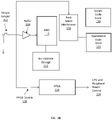
- FIG. 1A illustrates a system in normal operational mode, in accordance with one or more embodiments.
- a baseboard management controller (BMC) 110 runs code to control the system.
- a boot select mechanism 116 selects whether to boot the BMC from code stored in either a secure code store 120, or an operational code store 122.
- the system further includes non-volatile storage 112, a field programmable gate array (FPGA) 114, a buffer 104, and CPU and peripheral power control 124.
- the system may include more or fewer components than the components illustrated in FIG. 1A .
- the components illustrated in FIG. 1A may be local to or remote from each other.
- the components illustrated in FIG. 1A may be implemented in software and/or hardware. Each component may be distributed over multiple applications and/or machines. Multiple components may be combined into one application and/or machine. Operations described with respect to one component may instead be performed by another component.
- the BMC 110 is a controller that manages the system.
- Software running on the BMC can, among other things, monitor the system, power the system on or off, and install an operating system.
- the BMC includes software with the ability to determine whether the system is in normal operational mode, or secure mode.
- the BMC may be configured to fetch code from chip select zero. Chip select zero is a physical pin on the BMC that selects a particular code store.
- any type of controller known in the art may be used to perform the same functions.
- the BMC 110 may be implemented or may execute on the same computing system as the non-volatile storage 112, boot select mechanism 116, FPGA 116, secure code store 120, and operational code store 122.
- the BMC 110 may be implemented or executed on a computing system separate from the non-volatile storage 112, boot select mechanism 116, FPGA 116, secure code store 120, and operational code store 122.
- the BMC 110 may be communicatively coupled to the non-volatile storage or the boot select mechanism via a direct connection or via a network.
- the secure code store 120 is a location in the system where secure code is stored.
- the secure code store may be, for example, a flash memory, a physical location on a hard drive, or a virtual memory address.
- the secure code store 120 may include multiple different storage units and/or devices. The multiple different storage units and/or devices may or may not be of the same type or located at the same physical site.
- the secure code store In normal operational mode, the secure code store is electrically isolated from the boot select mechanism and the rest of the system (Isolation 118).
- the secure code, stored in the secure code store cannot be modified during normal operation.
- the secure code does not reference any other modifiable code.
- the secure code store may further store a replacement version of the operational code.
- the operational code store 122 is a location in the system where operational code is stored.
- the operational code store may be, for example, a flash memory, a physical location on a hard drive, or a virtual memory address.
- the operational code store 122 may include multiple different storage units and/or devices. The multiple different storage units and/or devices may or may not be of the same type or located at the same physical site.
- the operational code store is coupled to boot select mechanism 116.
- the operational code store may be communicatively coupled to the boot select mechanism via a direct connection or via a network.
- the operational code store may be coupled to the boot select mechanism by a Serial Peripheral Interface bus (SPI).
- SPI Serial Peripheral Interface bus
- the operational code store is coupled to the boot select mechanism, regardless of whether the system is in secure mode or operational mode.
- the operational code, stored in the operational code store is the code used for running the system during normal operation.
- the operational code may be the lowest level of code on the system.
- the boot select mechanism 116 includes hardware and/or software configured to control the boot device used by the BMC.
- the BMC may be configured to fetch code from an address mapped to chip select zero, as described above.
- the boot select mechanism may include functionality to manipulate what is seen by the BMC at chip select zero.
- the boot select mechanism points chip select zero to either the secure code store or the operational code store, depending on whether the system is in secure mode or operational mode. In operational mode, the secure code store is inaccessible, so the BMC cannot boot from or access the secure code store. In operational mode, the BMC may boot from the operational code store or another store (not shown) that is different from the secure code store.
- the buffer 104 is a one-way buffer coupled between the secure jumper and the BMC.
- the buffer includes functionality to prevents back-driving. Because the buffer is one-way, signals can only be transmitted to, not from, the BMC along that interface.
- the buffer 104 may further include functionality to temporarily store data as the data is transmitted to the BMC.
- the non-volatile storage 112 includes functionality to store data used by the system.
- the non-volatile storage is non-volatile memory, wherein the contents are saved when the system powers off.
- the non-volatile storage may be, for example read-only memory (ROM), programmable read-only memory (PROM), flash memory, a hard disk drive, or magnetic tape.
- the non-volatile storage 112 may include multiple different storage units and/or devices. The multiple different storage units and/or devices may or may not be of the same type or located at the same physical site.
- the non-volatile storage may be communicatively coupled to the BMC via a direct connection or a network.
- the FPGA 114 is an integrated circuit comprising an array of programmable logic blocks.
- the FPGA includes functionality to control the state of a component such as the CPU, peripheral power, add-in cards, and networks. For instance, the FPGA may control power to a device.
- the FPGA may be communicatively coupled to the CPU and peripheral power control via a direct connection or via a network.
- the CPU and peripheral power control 124 are communicatively coupled to the FPGA.
- the CPU is a processing unit used by the system to run software.
- the CPU may carry out instructions, based on the software.
- the peripheral power control may control power to the CPU and/or the system at large.
- the system In normal operation, in absence of the secure jumper, the system generates an FPGA enable signal 106.
- the FPGA enable signal enables the FPGA.
- the FPGA enable signal When the FPGA enable signal is active, the FPGA is operational.
- the FPGA may make internal changes to itself.
- the FPGA may transmit instructions to the CPU and peripheral power control. In normal operational mode, the FPGA may, for example, control power to the CPU.
- the system In absence of the secure jumper, the system also generates a signal to the BMC, so that the BMC may determine that normal operational mode is active. Further, a secure signal is transmitted to the boot select mechanism 116. The secure signal affects the boot selection logic of the boot select mechanism, such that the operational code store 122 is the boot device for the BMC.
- the secure code store 120 In normal operational mode, the secure code store 120 is isolated from the boot select mechanism, and the rest of the system (Isolation 118).
- the secure code store may be physically isolated, by severing the connection to the boot select mechanism, or by disconnecting power to the secure code store.
- the secure code store When the secure code store is isolated, it cannot be accessed by the rest of the system. In normal operational mode, the secure code store cannot be modified.
- the system may further comprise one or more operating systems, BIOS code sets, and applications (not pictured).
- FIG. 1B illustrates a system in secure mode, in accordance with one or more embodiments.
- the BMC 110, buffer 104, non-volatile storage 112, boot select mechanism 116, secure code store 120, operational code store 122, FPGA 114, and CPU and peripheral power control 124 are described above in Section 2 with reference to Fig. 1A , however, these components may be implemented or operate differently as noted below.
- the system is in the secure state as a result of the secure jumper 102 being inserted.
- the system may include more or fewer components than the components illustrated in FIG. 1B .
- the components illustrated in FIG. 1B may be local to or remote from each other.
- the components illustrated in FIG. 1B may be implemented in software and/or hardware. Each component may be distributed over multiple applications and/or machines. Multiple components may be combined into one application and/or machine. Operations described with respect to one component may instead be performed by another component.
- the secure jumper 102 is a physical shorting device that can be placed between two pins on a motherboard of the system.
- the secure jumper is grounded on one side.
- the secure jumper is coupled to the BMC 110 via buffer 104.
- the secure jumper connects the two pins electrically, changing the configuration of the system motherboard.
- the circuit connected to the BMC is configured to transmit the secure signal.
- the placement of the secure jumper changes the chip select hardware logic on the board, to change the boot device of the BMC via the boot select mechanism 116.
- the secure jumper triggers hardware on the motherboard, reconfiguring the code store attached to the service processor, and effectively changing the boot device. Additionally, when the secure jumper 102 is inserted, a secure signal is asserted. The secure signal is transmitted to the FPGA, the BMC (via buffer 104), and the boot select mechanism. With the secure jumper installed, the system is in secure mode.
- the secure signal transmitted to the FPGA, triggers an FPGA disable signal (126).
- the FPGA disable signal transmits an instruction to the FPGA, disabling the entire FPGA.
- the FPGA disable signal prevents the FPGA from running or communicating with any other devices.
- the FPGA disable signal secures the system from being interfered with by an untrusted entity within the FPGA while the system is in secure mode. The FPGA cannot cause any interference with the process of restoring a trusted firmware state.
- the FPGA is connected to the CPU and peripheral power control 124.
- the CPU and peripheral power control are in turn disabled, as they only can function through communication with the FPGA.
- secure mode the CPU and peripheral power control are disabled and logically isolated from the rest of the system.
- the secure signal further causes the secure code store to be connected to the BMC, by disabling the isolation.
- the BMC 110 may be communicatively coupled to the non-volatile storage or the boot select mechanism via a direct connection or via a network.
- the secure code store may be coupled to the boot select mechanism by a Serial Peripheral Interface bus (SPI).
- SPI Serial Peripheral Interface bus
- the secure signal affects the boot selection logic, such that the secure code store becomes the boot device for the BMC.
- the operational code store becomes, in effect, a secondary storage device.
- the system can only be reconfigured to or from secure mode by physically manipulating the system, by inserting or removing the secure jumper. The system cannot be reconfigured to or from secure mode by the execution of any code.
- the boot select mechanism points chip select zero to either the secure code store or the operational code store, depending on whether the system is in secure mode or operational mode.
- secure mode when both the secure code store and the operational code store are connected to the boot select mechanism, the boot select mechanism is configured to boot from the secure code.
- FIG. 2 illustrates an exemplary set of operations for restoring a trusted firmware state, in accordance with one or more embodiments.
- One or more operations illustrated in Figure 2 may be modified, rearranged, or omitted altogether. Accordingly, the particular sequence of operations illustrated in Figure 2 should not be construed as limiting the scope of one or more embodiments.
- System start up may include powering on one or more devices of the system.
- System start up may include booting one or more devices, based on software.
- the controller e.g., a BMC boots, based on the code stored in the selected code store.
- the selected code store is based upon the hardware configuration of the system.
- the system is either in secure mode, or not in secure mode (Operation 204). Whether the system is in secure mode is a matter of hardware logic, as determined by whether the secure jumper is inserted connecting two pins on the motherboard. Alternatively or additionally, the system may be configured to or from secure mode remotely, as described below in Section 6. As a result of the hardware logic, the system transmits one or more signals. Based on the signals, system components can determine the mode in effect.
- the controller executes the operational code, without access to the electrically-isolated secure code (Operation 220).
- Executing the operational code may include retrieving the operational code from the operational code store.
- the controller may retrieve the operational code from the operational code store physically, e.g., via a bus, or over a secure network.
- Executing the operational code may further include interpreting the operational code.
- the controller may perform a sequence of actions. For example, the controller may monitor the temperature of a processing unit of the system, based on instructions retrieved from the operational code store.
- the controller boots from the operational code store in normal operational mode.
- the secure code In absence of the secure jumper, the secure code is electrically isolated. Electrical isolation of the secure code may be achieved by physically severing the connection between the secure code store and the boot select mechanism. For example, the absence of the secure jumper disconnects a wire connecting the secure code store and the boot select mechanism.
- the hardware logic of the boot select mechanism is configured to select the operational code store as the boot device for the controller.
- the boot select mechanism may transmit boot device information to the controller, by transmitting an instruction that the operational code store is at chip select zero.
- the controller is configured to boot from chip select zero. The controller therefore boots from the operational code store, when not in secure mode.
- a signal sent to the controller from the motherboard, in absence of the secure jumper, is received by the controller as an input signal. This input signal allows the controller logic to determine that it is not operating in secure mode.
- Executing the secure code may include retrieving the secure code from the secure code store.
- the controller may retrieve the secure code from the secure code store physically, via a bus, or over a secure network.
- Executing the secure code may further include interpreting the secure code.
- the controller may perform a sequence of actions. For example, the controller may erase the software and/or memory stored to a particular device, based on instructions in the secure code.
- the motherboard With the secure jumper inserted into the motherboard, the motherboard is configured to transmit a secure signal.
- the secure signal is sent to the boot select mechanism, the controller, and the FPGA.
- the secure signal sent to the boot select mechanism, affects the boot selection logic.
- the secure signal causes the secure code store to be coupled to the boot select mechanism, and no longer disabled.
- the secure code is no longer isolated from the controller.
- the hardware logic of the boot select mechanism is configured to select the secure code store as the boot device for the controller.
- the boot select mechanism configures the system to boot from the secure code store.
- both the secure code store and the operational code store are connected to the boot select mechanism in secure mode, the boot select mechanism instructs the controller to boot from the secure code store.
- the boot select mechanism may transmit boot selection information to the controller.
- the boot select mechanism may transmit a notification to the controller that the secure code store is at chip select zero.
- the controller is configured to always boot from chip select zero. The controller therefore boots from the secure code store, when in secure mode.
- the system also transmits a secure signal to the controller.
- the controller receives the secure signal, as an input signal which cannot be back-driven.
- the placement of the buffer along the interface between the secure jumper and the controller prevents the controller from sending signals back towards the secure jumper.
- the controller cannot modify the secure signal. Due to receipt of the secure signal, the controller logic knows that it is operating in secure mode.
- the system transmits an FPGA disable signal to the FPGA.
- the FPGA disable signal prevents operation of the FPGA.
- the FPGA disable signal may cause the FPGA to be disabled, by cutting off power or clocks to the FPGA.
- the FPGA disable signal may cause the FPGA to be disabled by isolating the FPGA from other devices. When disabled, the FPGA cannot affect the state of any devices of the system. The FPGA cannot cause any interference with the process of restoring a trusted firmware state.
- the controller erases one or more code sets (Operation 212).
- the controller transmits an instruction to all devices that are not trusted, to erase the code and/or memory stored therein.
- the controller causes all programmable memory to be erased, which may include code sets stored to a peripheral service processor, NAND flash, non-volatile storage, or an FPGA.
- the controller may erase code sets such an operating system and/or a BIOS code set.
- the controller overwrites the current version of the operational code with a replacement version of the operational code referenced by the secure code (Operation 214).
- the secure code may include instructions to replace the operational code set with a version of the original operational code set that has been kept segregated in the secure code store.
- the operational code set may be replaced with a part of the original operational code set.
- the operational code set may be replaced with a boot loader. The steps described above can be executed without the need for any other firmware. Once the operations are complete, the entire system is cleaned and restored to a trusted firmware state.
- a user powers on the system with the secure jumper in place.
- the system is in secure mode.
- an FPGA disable signal is sent to the FPGA, disabling the FPGA, CPU, and peripheral power control.
- the system also transmits a secure signal to the boot select mechanism, causing it to disable the isolation of the secure code store.
- the secure signal affects the boot selection logic, in the boot select mechanism.
- the secure code store becomes the boot device for the controller.
- the system also transmits a secure signal to the controller.
- the controller receives the secure signal, as an input signal which cannot be back-driven. Due to receipt of the secure signal, the controller logic knows that it is operating in secure mode.
- the secure code store contains code instructing the controller to erase the code sets on the non-volatile storage, FPGA, and the operational code store.
- the secure code store further contains code that instructs the system to replace the code in the operational code store with a clean version of the operational code. After operating for a period of time, the operational code, in the operational code store, may have been altered, and possibly compromised.
- the controller in response to the instructions from the secure code, erases and replaces the codes.
- the operational code store contains clean code, but the code on the non-volatile storage and FPGA have not been replaced.
- a user reconfigures the system to normal operational mode. The operator physically removes the secure jumper. Removal of the secure jumper reconfigures the connection on the motherboard.
- the boot select hardware logic has been reconfigured to isolate the secure code store.
- the system transmits signals to the controller and the boot select mechanism, so that the controller boots from the operational code in the operational code store.
- the system transmits an FPGA enable signal to the FPGA.
- the FPGA is enabled, responsive to receipt of the FPGA enable signal.
- the operational code store is connected to the controller and the secure code store is not connected to the controller.
- the controller boots from the operational code in the operational code store.
- the secure code store is isolated from the system and cannot be compromised.
- the system executes operations to restore a server to a trusted firmware state.
- an operator powers off the system and inserts the secure jumper. The operator turns the power on, causing the BMC to boot.
- the BMC recognizes that the BMC is in secure mode, and boots from the secure code store.
- the BMC disables input from all external interfaces, and disables one or more devices of the system.
- the BMC may disable all untrusted devices and/or all devices that are not necessary for the execution of the secure code.
- the BMC may erase all non-volatile storage that it has access to, including the operational code store, the motherboard FPGA, non-volatile memory (e.g., NAND), and any other writable stores.
- the BMC reconstructs the operational code store using the contents of the secure code store.
- the BMC displays its status. In secure mode, the system will not boot all the way to the operating system. The BMC signals this by blinking an LED until all steps in secure mode are completed. Once the steps in secure mode have been completed, the BMC signals that the server has been restored to a trusted state, by altering the LED and displaying a message on a serial console.
- the operator turns the power off, and removes the jumper.
- the system sends enable signals instead of disable signals. Transmission of the enable signals causes the boot select mechanism to isolate and protect the secure code store, and configure the operational code store as the boot device.
- the BMC boots from the new, trusted code in the operational code store.
- the BMC loads a fresh firmware image.
- the fresh firmware image can be loaded from any trusted source, such as from a web server via network connection, or through a DVD.
- the BMC re-installs known good copies of all remaining firmware, such as BIOS, FPGA, and non-volatile memory. This can be done through normal firmware update procedure.
- the system is back in an operational state, and can operate from the newly restored root of trust.
- the system can be configured to and from secure mode remotely.
- the secure signal need not be asserted with a jumper.
- the secure signal is asserted using a trusted entity in the system, which allows remote administration of the system.
- the system includes a trusted entity.
- the trusted entity may be, for example, an add-in card with its own private interfaces.
- the trusted card is isolated from the rest of the system, and remains under control only by trusted users or devices.
- the trusted card may run on a simple microcontroller, to make it easy to verify that it is in a trusted state.
- the trusted entity manipulates signals in the system independently of the security model of the system. For example, the trusted entity can manipulate the secure signal, or the trusted entity can manipulate power to the system.
- the trusted entity is connected to the system logic, in place of the secure jumper.
- the trusted entity can receive an instruction from an external source.
- the trusted entity may then control the transmission of the secure signal, as described above.
- the trusted entity is communicatively coupled to a remote interface via a trusted remote connection.
- the trusted remote connection is private to any other interface connected to the system.
- the trusted remote connection may be a serial interface, and/or a network connection that only connects to a private network. By using the remote interface, an authorized user may alter the hardware configuration to or from secure mode.
- Embodiments are directed to a system with one or more devices that include a hardware processor and that are configured to perform any of the operations described herein and/or recited in any of the claims below.
- a non-transitory computer readable storage medium comprises instructions which, when executed by one or more hardware processors, causes performance of any of the operations described herein and/or recited in any of the claims.
- the techniques described herein are implemented by one or more special-purpose computing devices.
- the special-purpose computing devices may be hard-wired to perform the techniques, or may include digital electronic devices such as one or more application-specific integrated circuits (ASICs), field programmable gate arrays (FPGAs),or network processing units (NPUs) that are persistently programmed to perform the techniques, or may include one or more general purpose hardware processors programmed to perform the techniques pursuant to program instructions in firmware, memory, other storage, or a combination.
- ASICs application-specific integrated circuits
- FPGAs field programmable gate arrays
- NPUs network processing units
- Such special-purpose computing devices may also combine custom hard-wired logic, ASICs, FPGAs, or NPUs with custom programming to accomplish the techniques.
- the special-purpose computing devices may be desktop computer systems, portable computer systems, handheld devices, networking devices or any other device that incorporates hard-wired and/or program logic to implement the techniques.
- Figure 3 is a block diagram that illustrates a computer system 300 upon which an embodiment of the invention may be implemented.
- Computer system 300 includes a bus 302 or other communication mechanism for communicating information, and a hardware processor 304 coupled with bus 302 for processing information.
- Hardware processor 304 may be, for example, a general purpose microprocessor.
- Computer system 300 also includes a main memory 306, such as a random access memory (RAM) or other dynamic storage device, coupled to bus 302 for storing information and instructions to be executed by processor 304.
- Main memory 306 also may be used for storing temporary variables or other intermediate information during execution of instructions to be executed by processor 304.
- Such instructions when stored in non-transitory storage media accessible to processor 304, render computer system 300 into a special-purpose machine that is customized to perform the operations specified in the instructions.
- Computer system 300 further includes a read only memory (ROM) 308 or other static storage device coupled to bus 302 for storing static information and instructions for processor 304.
- ROM read only memory
- a storage device 310 such as a magnetic disk or optical disk, is provided and coupled to bus 302 for storing information and instructions.
- Computer system 300 may be coupled via bus 302 to a display 312, such as a cathode ray tube (CRT), for displaying information to a computer user.
- a display 312 such as a cathode ray tube (CRT)
- cursor control 316 is Another type of user input device
- cursor control 316 such as a mouse, a trackball, or cursor direction keys for communicating direction information and command selections to processor 304 and for controlling cursor movement on display 312.
- This input device typically has two degrees of freedom in two axes, a first axis (e.g., x) and a second axis (e.g., y), that allows the device to specify positions in a plane.
- Computer system 300 may implement the techniques described herein using customized hard-wired logic, one or more ASICs or FPGAs, firmware and/or program logic which in combination with the computer system causes or programs computer system 300 to be a special-purpose machine. According to one embodiment, the techniques herein are performed by computer system 300 in response to processor 304 executing one or more sequences of one or more instructions contained in main memory 306. Such instructions may be read into main memory 306 from another storage medium, such as storage device 310. Execution of the sequences of instructions contained in main memory 306 causes processor 304 to perform the process steps described herein. In alternative embodiments, hard-wired circuitry may be used in place of or in combination with software instructions.
- Non-volatile media include, for example, optical or magnetic disks, such as storage device 310.
- Volatile media include dynamic memory, such as main memory 306.
- Common forms of storage media include, for example, a floppy disk, a flexible disk, hard disk, solid state drive, magnetic tape, or any other magnetic data storage medium, a CD-ROM, any other optical data storage medium, any physical medium with patterns of holes, a RAM, a PROM, and EPROM, a FLASH-EPROM, NVRAM, any other memory chip or cartridge, content-addressable memory (CAM), and ternary content-addressable memory (TCAM).
- a floppy disk a flexible disk, hard disk, solid state drive, magnetic tape, or any other magnetic data storage medium
- CD-ROM any other optical data storage medium
- any physical medium with patterns of holes a RAM, a PROM, and EPROM
- FLASH-EPROM any other memory chip or cartridge
- CAM content-addressable memory
- TCAM ternary content-addressable memory
- Storage media are distinct from but may be used in conjunction with transmission media.
- Transmission media participate in transferring information between storage media.
- transmission media include coaxial cables, copper wire and fiber optics, including the wires that comprise bus 302.
- transmission media can also take the form of acoustic or light waves, such as those generated during radio-wave and infra-red data communications.
- Various forms of media may be involved in carrying one or more sequences of one or more instructions to processor 304 for execution.
- the instructions may initially be carried on a magnetic disk or solid state drive of a remote computer.
- the remote computer can load the instructions into its dynamic memory and send the instructions over a telephone line using a modem.
- a modem local to computer system 300 can receive the data on the telephone line and use an infra-red transmitter to convert the data to an infra-red signal.
- An infra-red detector can receive the data carried in the infra-red signal and appropriate circuitry can place the data on bus 302.
- Bus 302 carries the data to main memory 306, from which processor 304 retrieves and executes the instructions.
- the instructions received by main memory 306 may optionally be stored on storage device 310 either before or after execution by processor 304.
- Computer system 300 also includes a communication interface 318 coupled to bus 302.
- Communication interface 318 provides a two-way data communication coupling to a network link 320 that is connected to a local network 322.
- communication interface 318 may be an integrated services digital network (ISDN) card, cable modem, satellite modem, or a modem to provide a data communication connection to a corresponding type of telephone line.
- ISDN integrated services digital network
- communication interface 318 may be a local area network (LAN) card to provide a data communication connection to a compatible LAN.
- LAN local area network
- Wireless links may also be implemented.
- communication interface 318 sends and receives electrical, electromagnetic or optical signals that carry digital data streams representing various types of information.
- Network link 320 typically provides data communication through one or more networks to other data devices.
- network link 320 may provide a connection through local network 322 to a host computer 324 or to data equipment operated by an Internet Service Provider (ISP) 326.
- ISP 326 in turn provides data communication services through the world wide packet data communication network now commonly referred to as the "Internet" 328.
- Internet 328 uses electrical, electromagnetic or optical signals that carry digital data streams.
- the signals through the various networks and the signals on network link 320 and through communication interface 318, which carry the digital data to and from computer system 300, are example forms of transmission media.
- Computer system 300 can send messages and receive data, including program code, through the network(s), network link 320 and communication interface 318.
- a server 330 might transmit a requested code for an application program through Internet 328, ISP 326, local network 322 and communication interface 318.
- the received code may be executed by processor 304 as it is received, and/or stored in storage device 310, or other non-volatile storage for later execution.
Landscapes
- Engineering & Computer Science (AREA)
- Theoretical Computer Science (AREA)
- General Engineering & Computer Science (AREA)
- Physics & Mathematics (AREA)
- General Physics & Mathematics (AREA)
- Computer Hardware Design (AREA)
- Human Computer Interaction (AREA)
- Computer Security & Cryptography (AREA)
- Software Systems (AREA)
- Stored Programmes (AREA)
Claims (10)
- System, umfassend:eine Zentraleinheit CPU,einen Speicher (120) für sicheren Code, der einen Satz von in sich geschlossenem sicheren Code umfasst, der auf keinen anderen modifizierbaren Code verweist,einen Betriebscodespeicher (122), der einen Satz von Betriebscodes umfasst,eine Steuerung (110), die eine Funktionalität enthält, um beim Systemstart anfänglich eines von Folgendem auszuführen:(a) den Satz sicheren Codes, wenn das System mit einer ersten Hardwarekonfiguration konfiguriert ist, wobei die Ausführung des Satzes von sicherem Code das Überschreiben einer aktuellen Version des im Betriebscodespeicher gespeicherten Betriebscodes mit einer Ersatzversion des Betriebscodes umfasst, auf die durch den sicheren Code verwiesen wird, und(b) den Satz von Betriebscode, wenn das System mit einer zweiten Hardwarekonfiguration konfiguriert ist, wobei der sichere Codespeicher von einer oder mehreren anderen Komponenten des Systems elektrisch isoliert ist, wenn das System mit der zweiten Hardwarekonfiguration konfiguriert ist, wobei auf den Satz des sicheren Codes nicht zugegriffen werden kann, wenn das System mit der zweiten Hardwarekonfiguration konfiguriert ist, undeine integrierte Schaltung (114), die dazu beschaffen ist, einen Zustand der CPU zu steuern,wobei in der ersten Hardwarekonfiguration die integrierte Schaltung deaktiviert ist, so dass die CPU deaktiviert ist.
- System nach Anspruch 1, wobei die Ausführung des Satzes von sicherem Code ferner das Löschen eines Codesatzes umfasst, der einem oder mehreren von Folgendem entspricht:einem Betriebssystem,einem BIOS-Codesatz,einer Anwendung,einem NAND-Flash,einem nichtflüchtigen Speicher undeinem programmierbaren Logikgerät.
- System nach Anspruch 1, wobei die Ersatzversion des Betriebscodes, auf den durch den Satz von Sicherheitscodes verwiesen wird, innerhalb des Speichers für Sicherheitscodes gespeichert ist.
- System nach Anspruch 1, wobei die Ersatzversion des Betriebscodes, auf den durch den Satz von Sicherheitscodes verwiesen wird, außerhalb des Speichers für Sicherheitscodes gespeichert ist.
- System nach Anspruch 1, wobei ein Wechsel zwischen der ersten Hardwarekonfiguration und der zweiten Hardwarekonfiguration nicht ohne eine physische Manipulation des Systems bewirkt werden kann.
- System nach Anspruch 5, wobei die physikalische Manipulation des Systems umfasst: (a) Hinzufügen eines Jumpers zum Verbinden zweier Pins auf einer im System enthaltenen Hauptplatine oder (b) Entfernen des Jumpers zum Trennen zweier Pins auf einer im System enthaltenen Hauptplatine.
- System nach Anspruch 1, wobei ein Wechsel zwischen der ersten Hardwarekonfiguration und der zweiten Hardwarekonfiguration durch Fernmanipulation des Systems über eine in dem System enthaltene vertrauenswürdige Entität bewirkt werden kann.
- System nach Anspruch 1, wobei ein Wechsel von der zweiten Hardwarekonfiguration zu der ersten Hardwarekonfiguration nicht durch Ausführung irgendeines Codes bewirkt werden kann.
- System nach Anspruch 1, wobei die erste Hardwarekonfiguration ein oder mehrere Geräte deaktiviert, die für die Ausführung des sicheren Codes nicht erforderlich sind.
- System nach Anspruch 1, wobei die erste Hardwarekonfiguration ein oder mehrere Geräte deaktiviert, die eine Funktionalität beinhalten, um eine sichere Wiederherstellung des Systems zu stören, die durch den sicheren Code ermöglicht wird.
Applications Claiming Priority (2)
| Application Number | Priority Date | Filing Date | Title |
|---|---|---|---|
| US15/466,514 US10997296B2 (en) | 2017-03-22 | 2017-03-22 | System and method for restoration of a trusted system firmware state |
| PCT/US2017/063915 WO2018174969A1 (en) | 2017-03-22 | 2017-11-30 | System and method for restoration of a trusted system firmware state |
Publications (2)
| Publication Number | Publication Date |
|---|---|
| EP3602374A1 EP3602374A1 (de) | 2020-02-05 |
| EP3602374B1 true EP3602374B1 (de) | 2022-06-22 |
Family
ID=60766163
Family Applications (1)
| Application Number | Title | Priority Date | Filing Date |
|---|---|---|---|
| EP17817979.2A Active EP3602374B1 (de) | 2017-03-22 | 2017-11-30 | System und verfahren zur wiederherstellung eines sicheren zustands einer system-firmware |
Country Status (5)
| Country | Link |
|---|---|
| US (1) | US10997296B2 (de) |
| EP (1) | EP3602374B1 (de) |
| JP (1) | JP7200122B2 (de) |
| CN (1) | CN110494855B (de) |
| WO (1) | WO2018174969A1 (de) |
Families Citing this family (12)
| Publication number | Priority date | Publication date | Assignee | Title |
|---|---|---|---|---|
| US10997296B2 (en) | 2017-03-22 | 2021-05-04 | Oracle International Corporation | System and method for restoration of a trusted system firmware state |
| BE1026835B1 (de) * | 2018-12-06 | 2020-07-07 | Phoenix Contact Gmbh & Co | Router mit Anmeldungsfunktionalität und hierfür geeignetes Zugriffskontrollverfahren |
| US11829478B2 (en) * | 2019-01-08 | 2023-11-28 | Oracle International Corporation | Full server recovery architecture for cloud bare metal instances |
| US11288372B2 (en) | 2019-10-07 | 2022-03-29 | Microsoft Technology Licensing, Llc | Secure installation of baseboard management controller firmware via a physical interface |
| US11222120B2 (en) * | 2019-11-19 | 2022-01-11 | Dell Products L.P. | Storage device firmware bootloader recovery system and method therefor |
| US11314866B2 (en) | 2019-11-25 | 2022-04-26 | Dell Products L.P. | System and method for runtime firmware verification, recovery, and repair in an information handling system |
| US11099838B1 (en) * | 2020-02-26 | 2021-08-24 | Quanta Computer Inc. | Method and system for recovery for custom integrated circuit |
| CN115270100A (zh) * | 2021-04-29 | 2022-11-01 | 华为技术有限公司 | 一种安全保护方法、装置及系统 |
| US11783040B2 (en) | 2021-07-09 | 2023-10-10 | Dell Products L.P. | Cryptographically verifying a firmware image with boot speed in an information handling system |
| US11726879B2 (en) | 2021-07-12 | 2023-08-15 | Dell Products L.P. | Multiple block error correction in an information handling system |
| US20230132176A1 (en) * | 2021-10-21 | 2023-04-27 | Dell Products L.P. | Method and system for a secure management of storage devices using a key management service |
| CN114398013A (zh) * | 2022-01-26 | 2022-04-26 | 东芯半导体股份有限公司 | Nand存储器安全代码生成模块和生成方法、以及nand存储器 |
Family Cites Families (54)
| Publication number | Priority date | Publication date | Assignee | Title |
|---|---|---|---|---|
| US5388267A (en) * | 1991-05-29 | 1995-02-07 | Dell Usa, L.P. | Method and apparatus for updating and restoring system BIOS functions while maintaining BIOS integrity |
| JPH09330272A (ja) * | 1996-06-12 | 1997-12-22 | Hitachi Ltd | Bios制御方式 |
| US7257714B1 (en) * | 1999-10-19 | 2007-08-14 | Super Talent Electronics, Inc. | Electronic data storage medium with fingerprint verification capability |
| SE515327C2 (sv) * | 1999-08-27 | 2001-07-16 | Ericsson Telefon Ab L M | Anordning för att utföra säkra transaktioner i en kommunikationsanordning |
| US7930531B2 (en) * | 2000-01-06 | 2011-04-19 | Super Talent Electronics, Inc. | Multi-partition USB device that re-boots a PC to an alternate operating system for virus recovery |
| KR20030038542A (ko) * | 2000-05-19 | 2003-05-16 | 셀프 리페어링 컴퓨터스, 인크. | 스위칭 가능 소자를 가진 컴퓨터 |
| US6757838B1 (en) * | 2000-10-13 | 2004-06-29 | Hewlett-Packard Development Company, L.P. | Hardware independent implementation of computer system BIOS recovery |
| US7149854B2 (en) * | 2001-05-10 | 2006-12-12 | Advanced Micro Devices, Inc. | External locking mechanism for personal computer memory locations |
| TW548574B (en) * | 2001-10-19 | 2003-08-21 | Micro Star Int Co Ltd | Display interface with dual basic input/output system and the computer having the same |
| US7536598B2 (en) * | 2001-11-19 | 2009-05-19 | Vir2Us, Inc. | Computer system capable of supporting a plurality of independent computing environments |
| KR20040065495A (ko) * | 2003-01-14 | 2004-07-22 | 삼성전자주식회사 | 마이콤을 갖는 전자기기 및 그 펌웨어 갱신 방법 |
| US20040268116A1 (en) * | 2003-06-30 | 2004-12-30 | Vasisht Virender K | Fault tolerant recovery block with reduced flash footprint |
| JP2006081246A (ja) * | 2004-09-07 | 2006-03-23 | Yaskawa Electric Corp | シリアル通信指令方式サーボアンプ装置 |
| US20070157015A1 (en) * | 2005-12-29 | 2007-07-05 | Swanson Robert C | Methods and apparatus to optimize boot speed |
| US20080168310A1 (en) | 2007-01-05 | 2008-07-10 | Microsoft Corporation | Hardware diagnostics and software recovery on headless server appliances |
| US8924708B2 (en) | 2007-01-22 | 2014-12-30 | Simon Yoffe | Security switch |
| US8522309B2 (en) | 2007-01-22 | 2013-08-27 | Simon Yoffe | Security switch |
| US8250354B2 (en) * | 2007-11-29 | 2012-08-21 | GlobalFoundries, Inc. | Method and apparatus for making a processor sideband interface adhere to secure mode restrictions |
| US7861021B2 (en) * | 2008-01-24 | 2010-12-28 | International Business Machines Corporation | Device receiving unit that performs a determination based on data exchange which interfacing device takes precedence when a plurality of interfacing devices are simultaneously connected |
| JP5127511B2 (ja) * | 2008-03-04 | 2013-01-23 | キヤノン株式会社 | 光学装置 |
| TWI414996B (zh) * | 2008-04-14 | 2013-11-11 | Asustek Comp Inc | 電腦系統 |
| US8495349B2 (en) * | 2008-10-09 | 2013-07-23 | International Business Machines Corporation | Generating a primary BIOS code memory address and a recovery BIOS code memory address, where the recovery BIOS service code is loaded when the primary BIOS code fails to execute |
| US8341602B2 (en) * | 2009-01-29 | 2012-12-25 | Microsoft Corporation | Automated verification of a type-safe operating system |
| US8468592B2 (en) * | 2009-07-31 | 2013-06-18 | Google Inc. | Native code module security for 64-bit instruction set architectures |
| CN102419719A (zh) * | 2010-09-27 | 2012-04-18 | 鸿富锦精密工业(深圳)有限公司 | 电脑系统及电脑系统的开机方法 |
| CN102446103A (zh) * | 2010-10-08 | 2012-05-09 | 鸿富锦精密工业(深圳)有限公司 | Bios刷新装置及利用其进行bios数据刷新的方法 |
| CN102455945A (zh) * | 2010-10-27 | 2012-05-16 | 鸿富锦精密工业(深圳)有限公司 | 基板管理控制器恢复系统及其使用方法 |
| CN102455950A (zh) * | 2010-10-28 | 2012-05-16 | 鸿富锦精密工业(深圳)有限公司 | 基板管理控制器的韧体恢复系统及方法 |
| US8843769B2 (en) * | 2011-04-18 | 2014-09-23 | Texas Instruments Incorporated | Microcontroller with embedded secure feature |
| US8863109B2 (en) * | 2011-07-28 | 2014-10-14 | International Business Machines Corporation | Updating secure pre-boot firmware in a computing system in real-time |
| US8732527B2 (en) * | 2011-08-16 | 2014-05-20 | Google Inc. | Secure recovery apparatus and method |
| TWI537735B (zh) * | 2011-12-16 | 2016-06-11 | 祥碩科技股份有限公司 | 電子裝置及其基本輸入輸出系統的更新裝置 |
| WO2013102521A1 (en) * | 2012-01-03 | 2013-07-11 | International Business Machines Corporation | Method for secure self-booting of an electronic device |
| CN103246583A (zh) * | 2012-02-09 | 2013-08-14 | 鸿富锦精密工业(深圳)有限公司 | 具有bmc固件修复功能的电子装置及修复方法 |
| US9075995B2 (en) * | 2013-03-11 | 2015-07-07 | Microsoft Technology Licensing, Llc | Dynamically loaded measured environment for secure code launch |
| WO2014175861A1 (en) * | 2013-04-23 | 2014-10-30 | Hewlett-Packard Development Company, L.P. | Recovering from compromised system boot code |
| US20150052616A1 (en) * | 2013-08-14 | 2015-02-19 | L-3 Communications Corporation | Protected mode for securing computing devices |
| US9779241B2 (en) * | 2013-09-25 | 2017-10-03 | Cisco Technology, Inc. | Synchronization of UEFI secure boot variables on a managed server |
| TW201525858A (zh) * | 2013-12-31 | 2015-07-01 | Ibm | 基板管理控制器與其韌體載入方法 |
| US9135029B2 (en) * | 2014-01-02 | 2015-09-15 | Lenovo Enterprise Solutions (Singapore) Pte. Ltd. | Securely reconfiguring a multi-node system to prevent firmware rollback |
| US9075945B1 (en) * | 2014-06-27 | 2015-07-07 | Google Inc. | Method for implementing efficient entropy decoder by using high level synthesis |
| KR101931455B1 (ko) * | 2014-07-11 | 2018-12-20 | 피씨엠에스 홀딩스, 인크. | 가상화에 근거한 보안 디바이스를 위한 시스템 및 방법 |
| US20160306623A1 (en) * | 2015-04-16 | 2016-10-20 | Aic Inc. | Control module of node and firmware updating method for the control module |
| US9921915B2 (en) * | 2015-10-16 | 2018-03-20 | Quanta Computer Inc. | Baseboard management controller recovery |
| US10055296B2 (en) * | 2015-10-30 | 2018-08-21 | Quanta Computer Inc. | System and method for selective BIOS restoration |
| US9930051B1 (en) * | 2015-11-06 | 2018-03-27 | Amazon Technologies, Inc. | Remote management of hardware hosts in cloud infrastructure |
| US10133637B2 (en) * | 2016-08-04 | 2018-11-20 | Dell Products L.P. | Systems and methods for secure recovery of host system code |
| US10534618B2 (en) * | 2016-09-27 | 2020-01-14 | American Megatrends International, Llc | Auto bootloader recovery in BMC |
| US20180091315A1 (en) * | 2016-09-27 | 2018-03-29 | Qualcomm Incorporated | Revocation and updating of compromised root of trust (rot) |
| US10740468B2 (en) * | 2016-09-30 | 2020-08-11 | Hewlett Packard Enterprise Development Lp | Multiple roots of trust to verify integrity |
| US20180097839A1 (en) * | 2016-10-01 | 2018-04-05 | Neeraj S. Upasani | Systems, apparatuses, and methods for platform security |
| US10691803B2 (en) * | 2016-12-13 | 2020-06-23 | Amazon Technologies, Inc. | Secure execution environment on a server |
| US10997296B2 (en) | 2017-03-22 | 2021-05-04 | Oracle International Corporation | System and method for restoration of a trusted system firmware state |
| US10372460B2 (en) * | 2017-03-28 | 2019-08-06 | Dell Products, Lp | System and method for baseboard management controller assisted dynamic early host video on systems with a security co-processor |
-
2017
- 2017-03-22 US US15/466,514 patent/US10997296B2/en active Active
- 2017-11-30 WO PCT/US2017/063915 patent/WO2018174969A1/en unknown
- 2017-11-30 JP JP2019552048A patent/JP7200122B2/ja active Active
- 2017-11-30 EP EP17817979.2A patent/EP3602374B1/de active Active
- 2017-11-30 CN CN201780088689.XA patent/CN110494855B/zh active Active
Also Published As
| Publication number | Publication date |
|---|---|
| US10997296B2 (en) | 2021-05-04 |
| CN110494855A (zh) | 2019-11-22 |
| EP3602374A1 (de) | 2020-02-05 |
| CN110494855B (zh) | 2023-09-26 |
| US20180276385A1 (en) | 2018-09-27 |
| JP7200122B2 (ja) | 2023-01-06 |
| WO2018174969A1 (en) | 2018-09-27 |
| JP2020511727A (ja) | 2020-04-16 |
Similar Documents
| Publication | Publication Date | Title |
|---|---|---|
| EP3602374B1 (de) | System und verfahren zur wiederherstellung eines sicheren zustands einer system-firmware | |
| US7698704B2 (en) | Method for installing operating system on remote storage: flash deploy and install zone | |
| CN101202764B (zh) | 确定虚拟以太网适配器的链路状态的方法和系统 | |
| CN111989681A (zh) | 自动部署的信息技术(it)系统和方法 | |
| CN110073355A (zh) | 服务器上的安全执行环境 | |
| US9678682B2 (en) | Backup storage of vital debug information | |
| US20090100236A1 (en) | Copying data onto a secondary storage device | |
| CN1954297A (zh) | 在具有病毒、间谍软件以及黑客防护特征的虚拟处理空间中的隔离复用多维处理 | |
| EP3494471A1 (de) | Systeme und verfahren für die sichere wiederherstellung eines host-systemcodes | |
| CN105991651B (zh) | 具有远程存储控制的网络接口设备 | |
| US11860776B2 (en) | Concurrent memory recycling for collection of servers | |
| CN102253845B (zh) | 服务器系统 | |
| JP7441896B2 (ja) | システム特徴をセキュアに分離するためのシステムおよび方法 | |
| US11137995B2 (en) | Updating firmware of a microcontroller | |
| US20240134656A1 (en) | Self-contained worker orchestrator in a distributed system | |
| KR20060135757A (ko) | 바이러스, 스파이웨어, 및 해커 보호 특성을 갖는 가상처리 공간에서의 분리된 멀티플렉싱 다차원 처리 | |
| CN110647429A (zh) | 一种电子设备、处理系统及处理方法 |
Legal Events
| Date | Code | Title | Description |
|---|---|---|---|
| STAA | Information on the status of an ep patent application or granted ep patent |
Free format text: STATUS: UNKNOWN |
|
| STAA | Information on the status of an ep patent application or granted ep patent |
Free format text: STATUS: THE INTERNATIONAL PUBLICATION HAS BEEN MADE |
|
| PUAI | Public reference made under article 153(3) epc to a published international application that has entered the european phase |
Free format text: ORIGINAL CODE: 0009012 |
|
| STAA | Information on the status of an ep patent application or granted ep patent |
Free format text: STATUS: REQUEST FOR EXAMINATION WAS MADE |
|
| 17P | Request for examination filed |
Effective date: 20191016 |
|
| AK | Designated contracting states |
Kind code of ref document: A1 Designated state(s): AL AT BE BG CH CY CZ DE DK EE ES FI FR GB GR HR HU IE IS IT LI LT LU LV MC MK MT NL NO PL PT RO RS SE SI SK SM TR |
|
| AX | Request for extension of the european patent |
Extension state: BA ME |
|
| DAV | Request for validation of the european patent (deleted) | ||
| DAX | Request for extension of the european patent (deleted) | ||
| STAA | Information on the status of an ep patent application or granted ep patent |
Free format text: STATUS: EXAMINATION IS IN PROGRESS |
|
| 17Q | First examination report despatched |
Effective date: 20201015 |
|
| STAA | Information on the status of an ep patent application or granted ep patent |
Free format text: STATUS: EXAMINATION IS IN PROGRESS |
|
| GRAP | Despatch of communication of intention to grant a patent |
Free format text: ORIGINAL CODE: EPIDOSNIGR1 |
|
| STAA | Information on the status of an ep patent application or granted ep patent |
Free format text: STATUS: GRANT OF PATENT IS INTENDED |
|
| INTG | Intention to grant announced |
Effective date: 20220131 |
|
| GRAS | Grant fee paid |
Free format text: ORIGINAL CODE: EPIDOSNIGR3 |
|
| GRAA | (expected) grant |
Free format text: ORIGINAL CODE: 0009210 |
|
| STAA | Information on the status of an ep patent application or granted ep patent |
Free format text: STATUS: THE PATENT HAS BEEN GRANTED |
|
| AK | Designated contracting states |
Kind code of ref document: B1 Designated state(s): AL AT BE BG CH CY CZ DE DK EE ES FI FR GB GR HR HU IE IS IT LI LT LU LV MC MK MT NL NO PL PT RO RS SE SI SK SM TR |
|
| REG | Reference to a national code |
Ref country code: GB Ref legal event code: FG4D |
|
| REG | Reference to a national code |
Ref country code: CH Ref legal event code: EP |
|
| REG | Reference to a national code |
Ref country code: DE Ref legal event code: R096 Ref document number: 602017058810 Country of ref document: DE |
|
| REG | Reference to a national code |
Ref country code: AT Ref legal event code: REF Ref document number: 1500249 Country of ref document: AT Kind code of ref document: T Effective date: 20220715 |
|
| REG | Reference to a national code |
Ref country code: IE Ref legal event code: FG4D |
|
| REG | Reference to a national code |
Ref country code: LT Ref legal event code: MG9D |
|
| REG | Reference to a national code |
Ref country code: NL Ref legal event code: MP Effective date: 20220622 |
|
| PG25 | Lapsed in a contracting state [announced via postgrant information from national office to epo] |
Ref country code: SE Free format text: LAPSE BECAUSE OF FAILURE TO SUBMIT A TRANSLATION OF THE DESCRIPTION OR TO PAY THE FEE WITHIN THE PRESCRIBED TIME-LIMIT Effective date: 20220622 Ref country code: NO Free format text: LAPSE BECAUSE OF FAILURE TO SUBMIT A TRANSLATION OF THE DESCRIPTION OR TO PAY THE FEE WITHIN THE PRESCRIBED TIME-LIMIT Effective date: 20220922 Ref country code: LT Free format text: LAPSE BECAUSE OF FAILURE TO SUBMIT A TRANSLATION OF THE DESCRIPTION OR TO PAY THE FEE WITHIN THE PRESCRIBED TIME-LIMIT Effective date: 20220622 Ref country code: HR Free format text: LAPSE BECAUSE OF FAILURE TO SUBMIT A TRANSLATION OF THE DESCRIPTION OR TO PAY THE FEE WITHIN THE PRESCRIBED TIME-LIMIT Effective date: 20220622 Ref country code: GR Free format text: LAPSE BECAUSE OF FAILURE TO SUBMIT A TRANSLATION OF THE DESCRIPTION OR TO PAY THE FEE WITHIN THE PRESCRIBED TIME-LIMIT Effective date: 20220923 Ref country code: FI Free format text: LAPSE BECAUSE OF FAILURE TO SUBMIT A TRANSLATION OF THE DESCRIPTION OR TO PAY THE FEE WITHIN THE PRESCRIBED TIME-LIMIT Effective date: 20220622 Ref country code: BG Free format text: LAPSE BECAUSE OF FAILURE TO SUBMIT A TRANSLATION OF THE DESCRIPTION OR TO PAY THE FEE WITHIN THE PRESCRIBED TIME-LIMIT Effective date: 20220922 |
|
| REG | Reference to a national code |
Ref country code: AT Ref legal event code: MK05 Ref document number: 1500249 Country of ref document: AT Kind code of ref document: T Effective date: 20220622 |
|
| PG25 | Lapsed in a contracting state [announced via postgrant information from national office to epo] |
Ref country code: RS Free format text: LAPSE BECAUSE OF FAILURE TO SUBMIT A TRANSLATION OF THE DESCRIPTION OR TO PAY THE FEE WITHIN THE PRESCRIBED TIME-LIMIT Effective date: 20220622 Ref country code: LV Free format text: LAPSE BECAUSE OF FAILURE TO SUBMIT A TRANSLATION OF THE DESCRIPTION OR TO PAY THE FEE WITHIN THE PRESCRIBED TIME-LIMIT Effective date: 20220622 |
|
| PG25 | Lapsed in a contracting state [announced via postgrant information from national office to epo] |
Ref country code: NL Free format text: LAPSE BECAUSE OF FAILURE TO SUBMIT A TRANSLATION OF THE DESCRIPTION OR TO PAY THE FEE WITHIN THE PRESCRIBED TIME-LIMIT Effective date: 20220622 |
|
| PG25 | Lapsed in a contracting state [announced via postgrant information from national office to epo] |
Ref country code: SM Free format text: LAPSE BECAUSE OF FAILURE TO SUBMIT A TRANSLATION OF THE DESCRIPTION OR TO PAY THE FEE WITHIN THE PRESCRIBED TIME-LIMIT Effective date: 20220622 Ref country code: SK Free format text: LAPSE BECAUSE OF FAILURE TO SUBMIT A TRANSLATION OF THE DESCRIPTION OR TO PAY THE FEE WITHIN THE PRESCRIBED TIME-LIMIT Effective date: 20220622 Ref country code: RO Free format text: LAPSE BECAUSE OF FAILURE TO SUBMIT A TRANSLATION OF THE DESCRIPTION OR TO PAY THE FEE WITHIN THE PRESCRIBED TIME-LIMIT Effective date: 20220622 Ref country code: PT Free format text: LAPSE BECAUSE OF FAILURE TO SUBMIT A TRANSLATION OF THE DESCRIPTION OR TO PAY THE FEE WITHIN THE PRESCRIBED TIME-LIMIT Effective date: 20221024 Ref country code: ES Free format text: LAPSE BECAUSE OF FAILURE TO SUBMIT A TRANSLATION OF THE DESCRIPTION OR TO PAY THE FEE WITHIN THE PRESCRIBED TIME-LIMIT Effective date: 20220622 Ref country code: EE Free format text: LAPSE BECAUSE OF FAILURE TO SUBMIT A TRANSLATION OF THE DESCRIPTION OR TO PAY THE FEE WITHIN THE PRESCRIBED TIME-LIMIT Effective date: 20220622 Ref country code: CZ Free format text: LAPSE BECAUSE OF FAILURE TO SUBMIT A TRANSLATION OF THE DESCRIPTION OR TO PAY THE FEE WITHIN THE PRESCRIBED TIME-LIMIT Effective date: 20220622 Ref country code: AT Free format text: LAPSE BECAUSE OF FAILURE TO SUBMIT A TRANSLATION OF THE DESCRIPTION OR TO PAY THE FEE WITHIN THE PRESCRIBED TIME-LIMIT Effective date: 20220622 |
|
| PG25 | Lapsed in a contracting state [announced via postgrant information from national office to epo] |
Ref country code: PL Free format text: LAPSE BECAUSE OF FAILURE TO SUBMIT A TRANSLATION OF THE DESCRIPTION OR TO PAY THE FEE WITHIN THE PRESCRIBED TIME-LIMIT Effective date: 20220622 Ref country code: IS Free format text: LAPSE BECAUSE OF FAILURE TO SUBMIT A TRANSLATION OF THE DESCRIPTION OR TO PAY THE FEE WITHIN THE PRESCRIBED TIME-LIMIT Effective date: 20221022 |
|
| REG | Reference to a national code |
Ref country code: DE Ref legal event code: R097 Ref document number: 602017058810 Country of ref document: DE |
|
| PG25 | Lapsed in a contracting state [announced via postgrant information from national office to epo] |
Ref country code: AL Free format text: LAPSE BECAUSE OF FAILURE TO SUBMIT A TRANSLATION OF THE DESCRIPTION OR TO PAY THE FEE WITHIN THE PRESCRIBED TIME-LIMIT Effective date: 20220622 |
|
| PG25 | Lapsed in a contracting state [announced via postgrant information from national office to epo] |
Ref country code: DK Free format text: LAPSE BECAUSE OF FAILURE TO SUBMIT A TRANSLATION OF THE DESCRIPTION OR TO PAY THE FEE WITHIN THE PRESCRIBED TIME-LIMIT Effective date: 20220622 |
|
| PLBE | No opposition filed within time limit |
Free format text: ORIGINAL CODE: 0009261 |
|
| STAA | Information on the status of an ep patent application or granted ep patent |
Free format text: STATUS: NO OPPOSITION FILED WITHIN TIME LIMIT |
|
| 26N | No opposition filed |
Effective date: 20230323 |
|
| PG25 | Lapsed in a contracting state [announced via postgrant information from national office to epo] |
Ref country code: MC Free format text: LAPSE BECAUSE OF FAILURE TO SUBMIT A TRANSLATION OF THE DESCRIPTION OR TO PAY THE FEE WITHIN THE PRESCRIBED TIME-LIMIT Effective date: 20220622 |
|
| REG | Reference to a national code |
Ref country code: CH Ref legal event code: PL |
|
| P01 | Opt-out of the competence of the unified patent court (upc) registered |
Effective date: 20230526 |
|
| REG | Reference to a national code |
Ref country code: BE Ref legal event code: MM Effective date: 20221130 |
|
| PG25 | Lapsed in a contracting state [announced via postgrant information from national office to epo] |
Ref country code: LI Free format text: LAPSE BECAUSE OF NON-PAYMENT OF DUE FEES Effective date: 20221130 Ref country code: CH Free format text: LAPSE BECAUSE OF NON-PAYMENT OF DUE FEES Effective date: 20221130 |
|
| PG25 | Lapsed in a contracting state [announced via postgrant information from national office to epo] |
Ref country code: SI Free format text: LAPSE BECAUSE OF FAILURE TO SUBMIT A TRANSLATION OF THE DESCRIPTION OR TO PAY THE FEE WITHIN THE PRESCRIBED TIME-LIMIT Effective date: 20220622 Ref country code: LU Free format text: LAPSE BECAUSE OF NON-PAYMENT OF DUE FEES Effective date: 20221130 |
|
| PG25 | Lapsed in a contracting state [announced via postgrant information from national office to epo] |
Ref country code: IE Free format text: LAPSE BECAUSE OF NON-PAYMENT OF DUE FEES Effective date: 20221130 |
|
| PG25 | Lapsed in a contracting state [announced via postgrant information from national office to epo] |
Ref country code: FR Free format text: LAPSE BECAUSE OF NON-PAYMENT OF DUE FEES Effective date: 20221130 Ref country code: BE Free format text: LAPSE BECAUSE OF NON-PAYMENT OF DUE FEES Effective date: 20221130 |
|
| PGFP | Annual fee paid to national office [announced via postgrant information from national office to epo] |
Ref country code: GB Payment date: 20231012 Year of fee payment: 7 |
|
| PG25 | Lapsed in a contracting state [announced via postgrant information from national office to epo] |
Ref country code: IT Free format text: LAPSE BECAUSE OF FAILURE TO SUBMIT A TRANSLATION OF THE DESCRIPTION OR TO PAY THE FEE WITHIN THE PRESCRIBED TIME-LIMIT Effective date: 20220622 |
|
| PGFP | Annual fee paid to national office [announced via postgrant information from national office to epo] |
Ref country code: DE Payment date: 20231003 Year of fee payment: 7 |
|
| PG25 | Lapsed in a contracting state [announced via postgrant information from national office to epo] |
Ref country code: HU Free format text: LAPSE BECAUSE OF FAILURE TO SUBMIT A TRANSLATION OF THE DESCRIPTION OR TO PAY THE FEE WITHIN THE PRESCRIBED TIME-LIMIT; INVALID AB INITIO Effective date: 20171130 |
|
| PG25 | Lapsed in a contracting state [announced via postgrant information from national office to epo] |
Ref country code: CY Free format text: LAPSE BECAUSE OF FAILURE TO SUBMIT A TRANSLATION OF THE DESCRIPTION OR TO PAY THE FEE WITHIN THE PRESCRIBED TIME-LIMIT Effective date: 20220622 |