EP3602196B1 - Verfahren zur herstellung einer zeitmesskomponente und nach diesem verfahren erhaltene komponente - Google Patents
Verfahren zur herstellung einer zeitmesskomponente und nach diesem verfahren erhaltene komponente Download PDFInfo
- Publication number
- EP3602196B1 EP3602196B1 EP18712471.4A EP18712471A EP3602196B1 EP 3602196 B1 EP3602196 B1 EP 3602196B1 EP 18712471 A EP18712471 A EP 18712471A EP 3602196 B1 EP3602196 B1 EP 3602196B1
- Authority
- EP
- European Patent Office
- Prior art keywords
- resin
- layer
- process according
- substrate
- metal deposit
- Prior art date
- Legal status (The legal status is an assumption and is not a legal conclusion. Google has not performed a legal analysis and makes no representation as to the accuracy of the status listed.)
- Active
Links
Images






Classifications
-
- G—PHYSICS
- G03—PHOTOGRAPHY; CINEMATOGRAPHY; ANALOGOUS TECHNIQUES USING WAVES OTHER THAN OPTICAL WAVES; ELECTROGRAPHY; HOLOGRAPHY
- G03F—PHOTOMECHANICAL PRODUCTION OF TEXTURED OR PATTERNED SURFACES, e.g. FOR PRINTING, FOR PROCESSING OF SEMICONDUCTOR DEVICES; MATERIALS THEREFOR; ORIGINALS THEREFOR; APPARATUS SPECIALLY ADAPTED THEREFOR
- G03F7/00—Photomechanical, e.g. photolithographic, production of textured or patterned surfaces, e.g. printing surfaces; Materials therefor, e.g. comprising photoresists; Apparatus specially adapted therefor
-
- C—CHEMISTRY; METALLURGY
- C23—COATING METALLIC MATERIAL; COATING MATERIAL WITH METALLIC MATERIAL; CHEMICAL SURFACE TREATMENT; DIFFUSION TREATMENT OF METALLIC MATERIAL; COATING BY VACUUM EVAPORATION, BY SPUTTERING, BY ION IMPLANTATION OR BY CHEMICAL VAPOUR DEPOSITION, IN GENERAL; INHIBITING CORROSION OF METALLIC MATERIAL OR INCRUSTATION IN GENERAL
- C23C—COATING METALLIC MATERIAL; COATING MATERIAL WITH METALLIC MATERIAL; SURFACE TREATMENT OF METALLIC MATERIAL BY DIFFUSION INTO THE SURFACE, BY CHEMICAL CONVERSION OR SUBSTITUTION; COATING BY VACUUM EVAPORATION, BY SPUTTERING, BY ION IMPLANTATION OR BY CHEMICAL VAPOUR DEPOSITION, IN GENERAL
- C23C18/00—Chemical coating by decomposition of either liquid compounds or solutions of the coating forming compounds, without leaving reaction products of surface material in the coating; Contact plating
- C23C18/16—Chemical coating by decomposition of either liquid compounds or solutions of the coating forming compounds, without leaving reaction products of surface material in the coating; Contact plating by reduction or substitution, e.g. electroless plating
- C23C18/1601—Process or apparatus
- C23C18/1633—Process of electroless plating
- C23C18/1655—Process features
- C23C18/1657—Electroless forming, i.e. substrate removed or destroyed at the end of the process
-
- C—CHEMISTRY; METALLURGY
- C23—COATING METALLIC MATERIAL; COATING MATERIAL WITH METALLIC MATERIAL; CHEMICAL SURFACE TREATMENT; DIFFUSION TREATMENT OF METALLIC MATERIAL; COATING BY VACUUM EVAPORATION, BY SPUTTERING, BY ION IMPLANTATION OR BY CHEMICAL VAPOUR DEPOSITION, IN GENERAL; INHIBITING CORROSION OF METALLIC MATERIAL OR INCRUSTATION IN GENERAL
- C23C—COATING METALLIC MATERIAL; COATING MATERIAL WITH METALLIC MATERIAL; SURFACE TREATMENT OF METALLIC MATERIAL BY DIFFUSION INTO THE SURFACE, BY CHEMICAL CONVERSION OR SUBSTITUTION; COATING BY VACUUM EVAPORATION, BY SPUTTERING, BY ION IMPLANTATION OR BY CHEMICAL VAPOUR DEPOSITION, IN GENERAL
- C23C18/00—Chemical coating by decomposition of either liquid compounds or solutions of the coating forming compounds, without leaving reaction products of surface material in the coating; Contact plating
- C23C18/16—Chemical coating by decomposition of either liquid compounds or solutions of the coating forming compounds, without leaving reaction products of surface material in the coating; Contact plating by reduction or substitution, e.g. electroless plating
- C23C18/18—Pretreatment of the material to be coated
- C23C18/20—Pretreatment of the material to be coated of organic surfaces, e.g. resins
- C23C18/28—Sensitising or activating
- C23C18/285—Sensitising or activating with tin based compound or composition
-
- C—CHEMISTRY; METALLURGY
- C23—COATING METALLIC MATERIAL; COATING MATERIAL WITH METALLIC MATERIAL; CHEMICAL SURFACE TREATMENT; DIFFUSION TREATMENT OF METALLIC MATERIAL; COATING BY VACUUM EVAPORATION, BY SPUTTERING, BY ION IMPLANTATION OR BY CHEMICAL VAPOUR DEPOSITION, IN GENERAL; INHIBITING CORROSION OF METALLIC MATERIAL OR INCRUSTATION IN GENERAL
- C23C—COATING METALLIC MATERIAL; COATING MATERIAL WITH METALLIC MATERIAL; SURFACE TREATMENT OF METALLIC MATERIAL BY DIFFUSION INTO THE SURFACE, BY CHEMICAL CONVERSION OR SUBSTITUTION; COATING BY VACUUM EVAPORATION, BY SPUTTERING, BY ION IMPLANTATION OR BY CHEMICAL VAPOUR DEPOSITION, IN GENERAL
- C23C18/00—Chemical coating by decomposition of either liquid compounds or solutions of the coating forming compounds, without leaving reaction products of surface material in the coating; Contact plating
- C23C18/16—Chemical coating by decomposition of either liquid compounds or solutions of the coating forming compounds, without leaving reaction products of surface material in the coating; Contact plating by reduction or substitution, e.g. electroless plating
- C23C18/18—Pretreatment of the material to be coated
- C23C18/20—Pretreatment of the material to be coated of organic surfaces, e.g. resins
- C23C18/28—Sensitising or activating
- C23C18/30—Activating or accelerating or sensitising with palladium or other noble metal
-
- C—CHEMISTRY; METALLURGY
- C23—COATING METALLIC MATERIAL; COATING MATERIAL WITH METALLIC MATERIAL; CHEMICAL SURFACE TREATMENT; DIFFUSION TREATMENT OF METALLIC MATERIAL; COATING BY VACUUM EVAPORATION, BY SPUTTERING, BY ION IMPLANTATION OR BY CHEMICAL VAPOUR DEPOSITION, IN GENERAL; INHIBITING CORROSION OF METALLIC MATERIAL OR INCRUSTATION IN GENERAL
- C23C—COATING METALLIC MATERIAL; COATING MATERIAL WITH METALLIC MATERIAL; SURFACE TREATMENT OF METALLIC MATERIAL BY DIFFUSION INTO THE SURFACE, BY CHEMICAL CONVERSION OR SUBSTITUTION; COATING BY VACUUM EVAPORATION, BY SPUTTERING, BY ION IMPLANTATION OR BY CHEMICAL VAPOUR DEPOSITION, IN GENERAL
- C23C18/00—Chemical coating by decomposition of either liquid compounds or solutions of the coating forming compounds, without leaving reaction products of surface material in the coating; Contact plating
- C23C18/16—Chemical coating by decomposition of either liquid compounds or solutions of the coating forming compounds, without leaving reaction products of surface material in the coating; Contact plating by reduction or substitution, e.g. electroless plating
- C23C18/31—Coating with metals
- C23C18/32—Coating with nickel, cobalt or mixtures thereof with phosphorus or boron
-
- C—CHEMISTRY; METALLURGY
- C25—ELECTROLYTIC OR ELECTROPHORETIC PROCESSES; APPARATUS THEREFOR
- C25D—PROCESSES FOR THE ELECTROLYTIC OR ELECTROPHORETIC PRODUCTION OF COATINGS; ELECTROFORMING; APPARATUS THEREFOR
- C25D1/00—Electroforming
- C25D1/003—3D structures, e.g. superposed patterned layers
Definitions
- the present invention relates to a method for manufacturing a metallic watch component of complex shape with high precision, in an economical manner.
- the present invention also relates to the watch component thus obtained and a timepiece comprising said component.
- This process is derived from the LIGA technique (Lithographie Galvanoformung Abformung) which consists of depositing on a substrate a layer of 1 to 2000 ⁇ m of a photosensitive resin, of carrying out irradiation through a mask by means of a synchrotron or by a exposure to ultraviolet rays, to develop the irradiated (or non-irradiated) portions of the resin so as to form a resin mold, and to electroform a metal in this mold in order to obtain the micro metal part.
- LIGA technique Lithographie Galvanoformung Abformung
- Deposits made by electrodeposition tend to have an inhomogeneous and irregular surface due to the current field lines during galvanic growth.
- the production of components by electrodeposition therefore requires depositing the layer with an extra thickness and an additional rectification step (for example by polishing) in order to obtain an acceptable surface of the components.
- the document US2012/300596 A1 describes a process for manufacturing a watch component comprising the formation of a metallic deposit, used as a surface treatment, under electrical activation.
- the document entitled “New UV-LIGA type micro-structuring technologies and manufacturing of micromechanical components”, EPFL thesis 1770 (1998 ) describes the manufacture of a rotor by electroforming and a gear produced by chemical deposition of NiP-PTFE.
- the present invention relates to a method for manufacturing a watch component such as that which is the subject of claims 1 to 19, the resulting watch component as well as a timepiece comprising such a component.
- the active surface may consist of surfaces parallel to the face of the substrate and may include a first level which is the level closest to, or coincident with, the face.
- the active surface may include one or more second levels consisting of the next surfaces of a multi-stage mold.
- the metal deposit preferably has a thickness of at least 100 ⁇ m.
- chemical metallization refers exclusively to chemical metallizations free from electrical activation, such as for example autocatalysis.
- electrochemical metallization refers to current-activated metallizations, such as electrodeposition and electroplating.
- the metal deposition can be carried out in any metal capable of being deposited by a chemical metallization process, in particular a metal based on nickel or an alloy at least partly metallic based on nickel; by way of non-limiting example, a deposit of nickel phosphorus can be made from a bath of chemical nickel comprising the element phosphorus.
- the deposit can comprise between 2% and 20% phosphorus, preferably between 4% and 15% and can have a hardness of more than 400Hv, or even 500Hv.
- the structurable resin is deposited with a thickness greater than 100 ⁇ m; the thickness that can be obtained in one or more deposition steps.
- the deposit can be obtained in different ways, such as for example by spin-coating or by application of an adhesive film.
- the process disclosed here combines the advantages of chemical deposition combined with a structured resin, that is to say, the possibility of economically manufacturing a complex component of high precision without the disadvantages brought by electroplating, in particular the problems of current distribution across the entire substrate and structures in the resin mold.
- FIG. 1 shows an example of a substrate 10 comprising a face 11 intended to receive a structurable resin 20.
- THE figures 2a And 2b schematically illustrate a process for manufacturing a metal watch component, according to one embodiment.
- the process is based on selective deposition of the metal using a layer of structured resin 20.
- the method comprises the steps of providing a substrate 10 comprising at least one face 11 on which a layer of structurable resin 20 is applied, directly or on one or more intermediate layers.
- the layer of resin 20 is then structured so as to form openings 21 in it which reveal an active surface 14, that is to say a surface intended to receive the metallic deposit.
- the active surface 14 can correspond to the exposed portions of the face 11 which are not covered by the resin 20, comprising a first primer layer (variant 1), or on the substrate itself (variant 2).
- the active surface 14 can also correspond to a first level 14' located on a resin layer, as illustrated in 3, defining in a similar manner the bottom 21 of the resin mold 20.
- Variant 4 shows the structured resin layer 20 having several levels (second levels 14" of the active surface 14).
- the shape of the contour of the openings 22 corresponds substantially in the shape of the component 41 to be produced.
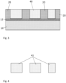
- a metal deposit 40 is then formed in the openings 21 of the structured resin layer 20 (which then forms a mold) by deposition of the metal (see the Figure 3 ).
- the mold By distributing the mold over several faces of the substrate, such as for example the two main faces of a substrate, which may for example have substantially the shape of a disk, it is possible to advantageously increase the number of components produced during of the same stage of a metal deposit.
- the metal deposit 40 formed is released from the resin 20 and the substrate 10 in order to obtain the component 41 (see the Figure 4 ).
- the particularity of the present process is that the metal deposit 40 is obtained by a chemical metallization process (electroless metal plating).
- the substrate 10 comprises a first primer layer 12 on the face 11, the metal deposit 40 being formed on the portions not being covered by the resin 20 (active surface 14).
- the first primer layer 12 is a catalytic layer or capable of being made catalytic.
- the first primer layer 12 may only partially cover the face 11 and/or the active surface 14.
- the first primer layer 12 may have a monatomic thickness or a certain thickness, or else be continuous or discontinuous.
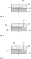
- FIG. 5 illustrates the formation of the first primer layer 12 before deposition of the structurable resin 20, in which the primer layer 12 can cover the face 11 of the substrate 10 totally or partially.
- the first primer layer 12 can be formed on an adhesion and/or sacrificial layer 15 deposited on the substrate 10 before deposition of the structurable resin 20.
- adhesion is meant that the layer 15 facilitates the adhesion of the first primer layer 12, and by sacrificial, we mean that layer 15 facilitates the separation of the metal deposit from the substrate.
- FIG. 6 illustrates the formation of a first primer layer 12 on the face 11 of the substrate 10, as well as an insulating layer 13, that is to say a non-catalytic layer, formed on the first primer layer 12, before deposition of the structurable resin 20.
- the formation of layer 13 can be obtained by deposition or by reaction of the material of layer 12, such as for example metallic oxidation.
- FIG. 7 illustrates the first primer layer 12 which can comprise at least one portion of structured surface 120 and which is formed on the face 11.
- the first primer layer 12 can cover at least a portion of the face 11.
- at least a portion of surface we mean a part or the entirety of the surface.
- FIG 8 illustrates a variant in which the structurable resin 20 is deposited directly on the face 11 of the substrate 10 which can include a structuring 120 at least on a portion of the face 11.
- the substrate 10 can be made of a catalytic material or capable of being made catalytic.
- the first primer layer 12 is the face 11 of the substrate 10, and constitutes the first level 14' of the active surface 14 after obtaining the mold.
- FIG. 9 shows the variant of the Figure 6 after exposure and development of the structurable resin 20 and removal of the insulating layer 13 in the bottom of the openings 21 thus produced.
- the steps of applying the layer of structurable resin 20 and structuring the resin 20 are repeated in order to obtain a multi-level mold.
- the metal deposit 40 is formed in the openings 21 of the resin layer 20, once the multi-level mold has been formed.
- a multi-level mold is preferably produced with levels defined by geometries whose surface area increases starting from the first level on the substrate side, and whose geometry includes that of the opening made in the previous level, as by example illustrated in the figures 13 to 15 .
- a second conductive but non-catalytic primer layer 12' is formed on at least a portion of the second levels 14" of the active surface 14.
- the metal deposit 40 is formed at each of the steps of applying the layer of structurable resin 20 and of structuring the resin 20.
- the steps of applying the layer of structurable resin 20, of structuring the resin 20 and to form the metal deposit 40 are repeated in order to obtain a mold, filled with metal, at several levels.
- a second primer layer 12' which can be formed on at least a portion of the second levels 14" of the active surface 14 (see variant 4 in the figures 2a And 2b ), can be conductive and/or catalytic.
- it is possible to produce a multi-material component two levels being able to be produced in different materials.
- the same level of the component can also be made with more than one material, this making it possible to adapt the properties of each level of the component to the constraints to which it is subjected during its implementation in a mechanism.
- FIG. 10 illustrates the formation of a second primer layer 12' on the first level of a layer of structurable resin 20, before structuring.
- the second primer layer 12' can be formed on all or a portion of the face of the first level of the structurable resin layer 20.
- the second primer layer is in this case preferably conductive but not catalytic.
- FIG. 11 illustrates the formation of the second primer layer 12' on a first level of the structurable resin layer 20 after structuring.
- the primer layer 12' can be formed on all or a portion of the face of the first level of the structurable resin layer 20.
- the second primer layer is in this case preferably conductive but not catalytic.
- FIG. 12 illustrates the formation of the second primer layer 12' on a first level of the structurable resin layer 20 after structuring and after the deposition of a metal deposit 40 in the openings 21.
- the second primer layer 12' can be formed on all or a portion of the face of the first level of the structurable resin layer 20.
- the second primer layer 12' can therefore only cover the resin 20, the metal 40 or both.
- the primer layer can in this case be catalytic and/or conductive.
- FIG 13 illustrates the formation of a second level 20' of the structurable resin layer 20, after structuring of the previous level.
- a second primer layer 12' is included between a first level 20 of resin and the second level 20' of resin.
- the formation of the second level of resin 20' can be carried out before (for example Figure 15 ) or after (for example figures 10 to 14 ) the formation of a second primer layer 12' on the first level of structurable resin 20.
- the second level of resin 20' can be formed before the structuring of the first level of resin 20.
- the second primer layer is in this case preferably conductive but not catalytic.
- FIG. 14 illustrates the formation of a second level of resin 20', after structuring and deposition of the metal 40.
- a second primer layer 12' is formed on the first level of resin 20, before or after formation of the second level of resin 20'.
- the second primer layer 12' can in this case be catalytic and/or conductive.
- FIG. 15 illustrates the formation of a first primer layer 12 on the active surface 14 exposed by the openings 21 formed in the first level and of a second primer layer 12' on the surfaces parallel to the layers of the mold and exposed by the following levels of the resin mold.
- the active surface 14 comprises an exposed portion of the face 11 of the substrate 10 and an exposed portion of the first resin level 20 and can consist of a first primer layer 12 as well as a second primer layer 12 '.
- the method implements the use of a substrate 10 comprising a structure 16 in which the metal 40 can be deposited, for example by forming an active surface at the bottom of an opening of a layer of resin 20.
- the active surface 14 being in this case preferably obtained by the formation of a first primer layer 12, not illustrated but like that described in the examples of the figures 5 to 7 , made in the bottom of the structure 16 of the substrate.
- the active surface can be obtained by the formation of a catalytic layer or capable of being made catalytic or by the use of a catalytic substrate or capable of being made catalytic. catalytic.
- the prior structuring of the substrate offers the advantage of being able to produce a multilevel metal deposit 40 of which at least one level is obtained by the structuring of the substrate.
- the structurable resin mold can then include only one level, the other additional level(s) conforming to the structuring 16 of the substrate. It also makes it possible to produce geometries with non-vertical sides, such as bevels for example.
- the structure can also consist of a decoration which will be made on the substrate in the form of a negative imprint, to obtain the positive form on the component obtained. In this case, the negative imprint can be made set back from the main surface of the substrate which receives the layer of photostructurable resin, in a projecting manner, or a combination of the two.
- a variant still allows the geometries of the two techniques to be combined, such as for example a watch component comprising a drop and a hole in its center.
- the outer contour of the drop does not need to be as precise as the rest of the component and can result from the substrate structuring process.
- the through hole of the component can be produced during a single structuring and metal deposition step, in the two levels (the structure 16 and the resin layer 20) of the hybrid mold.
- FIG. 17 illustrates a variant of the method comprising a step of forming a structured layer 17 on the face 11 of the substrate 10.
- the structured layer 17 comprises openings 170 revealing an active surface 14, corresponding to that of the substrate 10 or to that of a layer covering the face 11 of the substrate 10, such as a first primer layer 12 or any variant proposed in the examples of the figures 1 to 8 .
- the blanks of the openings 170 of the structured layer 17 may comprise one or more patterns 171 so that the metal deposit 40 deposited in the opening(s) 170 comprises structured geometries such as threads, knurling or any other geometry involving structures. on the vertical sides of the metal deposit 40.
- the structured layer 17 can be deposited on the substrate after structuring, and can be made of any material, including a structurable resin.
- FIG. 18 illustrates a variant of the process in which an insert 18 is integrated into the metal deposit 40.
- the insert 18 can be made from a metallic or non-metallic catalytic material, such as for example a ceramic or other material, taking care to passivate its vertical sides in the case of a catalytic or conductive material.
- the insert 18 makes it possible to add, for example, complex structures (threads, etc.) on the sides of the deposited metal 40 as well as on its surfaces, the faces of the insert adjacent to the exterior faces of the metal deposit 40 produced being able to be structured and/or the insert 18 made of a particular material so as to allow extended functionalities of the component 41.
- the insert 18 can also be used for screwing, driving, guiding another component, etc., of the component 41 produced by the present process.
- the metal deposit 40 produced in a mold composed of a single layer of structured resin 20 or a mold composed of several levels of layers of structured resin 20 can be leveled or brought to thickness, for example by lapping.
- the thickness setting can be carried out for each step of deposition of the metal in a level.
- the layer of structurable resin 20 can also be set to thickness before structuring or after structuring.
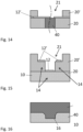
- Figure 19 illustrates a machining process (counterboring, in this case) on a first face 42 of the metal deposit 40
- Figure 20 illustrates a machining process (for example beveling with a beveling tool 44 on a second face 43 of the metal deposit 40, after having previously turned over the layer of metallized resin 20.
- a support element 10' is mounted integrally (for example with a holding and/or sacrificial layer 15', as illustrated, to facilitate its holding and/or its separation) on the side of the metal deposit 40 (second face 42 of the metal deposit 40) opposite the substrate, the substrate then being removed (by delamination, dissolution, etc.), thus making it possible to release the first face of the metal deposit 40.
- This variant makes it possible in particular to produce non-vertical geometries, difficult to produce in a structured resin mold 20, in particular when the structuring is carried out by exposure to rays substantially perpendicular to the surface of the substrate.
- the variant illustrated in Figure 16 can be preceded by a step of filling the structuring produced in the substrate 10 with a layer of structurable resin 20 so as to obtain a level of the structured mold included in the thickness of the substrate and which can be defined by the structuring of the substrate and an optional step of structuring this resin layer 20.
- the process disclosed here makes it possible to economically produce complex, high-precision components up to medium-sized series.
- chemical metallization is advantageous over electrochemical metallization conventionally used for the growth of a metal in a structured resin mold.
- Chemical metallization is an auto-catalytic reaction which does not require the passage of a current in the deposition bath. For this reason, deposition facilities can be simpler and lower cost than in the case of galvanic deposition. It is also not necessary to know the area of the surfaces to be deposited in order to adapt the density of the deposition current.
- the growth of the deposit is also more regular and homogeneous than in the case of galvanic deposition, thus making it possible to eliminate the rectification step or at least to reduce the rectification time, for example, to obtain a mirror polish.
- the surfaces of the substrate 10 and of the structured resin 20 on which the metal is deposited must allow the initiation of the deposition, that is to say they must be made catalytic, or capable of being made catalytic, to a chemical deposition and made conductive, or capable of being made conductive, for an electrochemical deposition, and preferably cleaned.
- Obtaining a first primer layer 12 for the growth of the first level of the metal deposit can be obtained by any process allowing the formation of a catalytic layer or the activation of a material capable of being made catalytic.
- a material capable of being made catalytic we mean making it catalytic by changing its passivation potential or, in the case of a conductive and non-catalytic material, by putting it in contact with a catalytic material, which also makes it catalytic.
- a catalytic material which also makes it catalytic.
- gold is catalytic in a bath comprising boron, and conductive but not catalytic in a bath comprising phosphorus. In the latter case, it can be made catalytic by placing it in contact with a catalytic material, such as for example iron.
- a variant consists of depositing a catalytic material, such as for example platinum or palladium.
- a catalytic layer can be obtained by salt chemistry, which includes in particular the chemical reduction of catalytic metal salts, the use of photosensitive metal salts, such as for example silver salts (silver process), chlorides of gold, a solution of iron oxalate salts and platinum or palladium salts (platinotype process), or even the use of surface catalyst salts.
- the steps of deposition of photosensitive salts can include several steps whose order can be changed, certain steps can even be deleted.
- the deposition of photosensitive salts can be done on all or part of the primer surfaces to make them catalytic. This deposition can be done on a previously functionalized surface to allow better adhesion of the primer layer to the substrate. This step can therefore be carried out at several points in the process of producing the structured mold. Thus, it can for example be done before deposition of the first layer of structurable resin 20, after deposition of the structurable resin 20, and in this case, before or after exposure of the resin, or even after obtaining the mold by structuring. It is thus possible to generate a first partial or entire primer layer 12 on the first level of a mold, and this at several points in the process.
- the deposition of salts is generally carried out by immersion in a bath containing such salts, this technique being similar to the processes used in photography processes, particularly film photography.
- solutions containing silver salts such as a silver nitrate, a silver acetate, a silver oxalate, a silver halide or even a silver perchlorate can be used, although this last category presents risks linked to its handling.
- the salts are subjected to total or partial light exposure, in particular in order to make selective deposits, to freeze them on the surface.
- This revelation operation especially in the case of silver nitrate, gives metallic silver on the exposed parts, which makes the surface locally catalytic.
- the metallic silver is not catalytic, it is necessary to replace part of the metallic silver with platinum, palladium, gold or other precious metals. an oxidation-reduction reaction with salts of platinum, palladium, gold or other precious metals and the metal silver.
- An optional step of revealing the salts exposed in a developer, such as hydroquinone, makes it possible to obtain larger metal aggregates, thus making the surface more catalytic, which may be preferable to promote the initiation of growth in a chemical metallization process.
- a developer such as hydroquinone
- the metal deposition 40 can use a first step of metal deposition by chemical means on a first level, from a first layer of catalytic primer 12, and a subsequent step of metal deposition by electrochemical means (electrodeposition) on a next level, from a second primer layer 12' constituted by a conductive and/or catalytic surface (for example, in the case of a primer layer by metal salts, sufficiently close spacing of the catalytic salts allows growth by nucleation of the metal deposit).
- the substrate 10 and the structured resin 20 comprise an active surface 14 made or capable of being made catalytic from which the metal deposition is made.
- the substrate 10 can itself be non-catalytic and comprise, on its face 11, a first primer layer 12.
- the substrate 10 can comprise a silicon plate on the surface (face 11) of which is produced a first layer of catalytic primer 12.
- the substrate 10 may comprise a glass or a ceramic.
- the primer layer 12 is a conductive layer, this may in particular be a layer of nickel, copper, iron, platinum, palladium, stainless steel, gold or another metal and/or a combination of these layers.
- the substrate 10 can be made of a catalytic metallic material or capable of being made catalytic and can comprise, for example, an alloy comprising at least one metallic element chosen from aluminum, copper, iron, platinum, palladium, nickel, gold, or other suitable metal or alloy.
- a metal substrate 10 has the advantage of having a thermal expansion coefficient close to that of the deposited metal.
- a nickel phosphorus (NiP) is typically deposited at a temperature between approximately 70°C to 95°C. As it cools, a silicon substrate could strain slightly. This effect will be reduced with a metal substrate whose thermal expansion coefficient is close to that of the material deposited.
- catalytic material substrates may include a polymer, ceramic or glass doped with catalytic elements such as catalytic metal nano- and/or microparticles.
- a catalytic ceramic such as titanium nitride for example, can be used.
- the substrate 10 can be made of a non-catalytic and/or non-conductive material such as a polymer, a composite, a glass, a ceramic or a non-catalytic metal, the face 11 of the substrate 10 receiving the deposit 40 then being made catalytic, in part or entirely, by appropriate means.
- a non-catalytic and/or non-conductive material such as a polymer, a composite, a glass, a ceramic or a non-catalytic metal
- the face 11 of the substrate 10 receiving the deposit 40 then being made catalytic, in part or entirely, by appropriate means.
- Metals with low adhesion power such as gold, stainless steel, certain chromium alloys or aluminum may be favored to facilitate the removal of components.
- metal salts or chlorides can be used, such as for example salts of precious elements (such as silver, platinum, palladium or even gold). These salts may or may not be photo-reduced and/or chemically reduced.
- a second primer layer can be obtained by depositing a conductive material.
- This layer can be formed in different ways, such as for example by vapor phase deposition (generally PVD) or chemical phase deposition (generally CVD).
- PVD vapor phase deposition
- CVD chemical phase deposition
- different processes can be used, such as for example sparing or lift-off, to cover only the desired part of the surface, or even etching after deposition, to remove the parts not covered. desired layer.
- the structurable resin 20 will be chosen from the group comprising photosensitive resins, these being able to be of positive or negative type.
- the resin 20 is applied to the face 11 of the substrate 10.
- the resin 20 comprises a negative photosensitive resin based on epoxy.
- the resin may comprise an octofunctional epoxy resin of the SU-8 type which polymerizes under the action of UV radiation. Other resins can react to x-ray type radiation.
- the structuring of the resin layer 20 consists of irradiating through a mask 30 (see the figure 2 ), the layer of resin 20 previously applied to the face 11 of the substrate 10. This layer of resin 20 is polymerized according to the pattern of the mask 30 and the unpolymerized parts of the layer are eliminated by chemical means. The remaining part of resin 20 forms a mold comprising one or more cavities 21 and defining the contour 22 of the component 41.
- annealing of the photosensitive resin layer causes polymerization in areas that have received UV radiation. This polymerized part becomes insensitive to most solvents as opposed to the non-irradiated areas which are dissolved by a solvent.
- the structuring of the resin layer 20 consists of developing the non-exposed areas of the photosensitive resin layer 20 to reveal in places, that is to say in the openings 21, the face 11 of the substrate 10 (these exposed portions of face 11 then correspond to active surface 14).
- this operation can be carried out by dissolving the non-exposed areas using a solvent chosen from GBL (gammabutyrolactone) and PGMEA (propylene glycol methyl ethyl acetate).
- GBL gammabutyrolactone
- PGMEA propylene glycol methyl ethyl acetate
- the resin layer 20 can be deposited on the substrate 10 with a thickness of at least 50 ⁇ m, or even at least 100 ⁇ m. Depending on the type of resin used, it may be necessary to successively deposit more than one layer of resin 20 on the substrate 10 in order to achieve the thickness of the desired resin layer.
- the structurable resin will be chosen from the group comprising radiation-curable resins.
- the structuring is preferably done by exposure to an electron beam source.
- This process is most often referred to as e-beam lithography and has a number of advantages, including increased precision, in the nanometer range. While engraving by “e-beam lithography” is most often carried out without a mask, in a serial manner, it is also possible to combine it with the use of masks, which makes the process faster and overcomes speed problems. encountered in the application of the process without a mask. Such a possibility has already been presented in the documents US3544790 And US3681103 .
- a metal deposit 40 is then produced in the openings 21 of the resin mold 20 by a chemical metallization process, this chemical metallization being able to be combined, in a subsequent step, with a galvanic metallization step.
- the metal deposit 40 can be raw up to a thickness less than that of the resin layer 20, substantially the same thickness, or even beyond the upper surface of the resin 20.
- Figure 3 shows a metal deposit 40 produced substantially at the same thickness as the resin layer 20.
- the metal deposit 40 may comprise a layer of chemical nickel (or one of its alloys) or a layer obtained by chemical nickel plating.
- Electroless nickel plating is an electroless deposition process that occurs in the presence of a reducing agent, such as sodium hydrophosphite (NaPO 2 H 2 ⁇ H 2 O) that reacts with metal ions to deposit the metal.
- a reducing agent such as sodium hydrophosphite (NaPO 2 H 2 ⁇ H 2 O) that reacts with metal ions to deposit the metal.
- Nickel can be deposited with different percentages of phosphorus, for example between 2% and 5% (low phosphorus content), between 5% and 8% (medium phosphorus content) or between 8% and 15% (high phosphorus content). ), or even between 15% and 20%.
- the hardness without heat treatment of the chemical phosphorus nickel deposit is typically between 520 HV for low phosphorus content and 650 HV for high phosphorus content.
- compositions allowing thick deposits can be used, and more particularly but not limited to, baths containing at least one element from a group including cobalt, boron, phosphorus, nickel, copper and gold.
- baths containing at least one element from a group including cobalt, boron, phosphorus, nickel, copper and gold can be used, and more particularly but not limited to, baths containing at least one element from a group including cobalt, boron, phosphorus, nickel, copper and gold.
- These metals or alloys can further incorporate one or more elements including tungsten, molybdenum, chromium, tin, iron, to obtain alloys with modified properties.
- salts of these metals added to the base baths are co-reduced to improve properties such as hardness, coefficient of friction, magnetism or even the properties of expansion and thermoelasticity.
- the metal deposit 40 can be produced in the openings 21 with a thickness of at least 50 ⁇ m and preferably at least 100 ⁇ m. Thicknesses of the metal deposit 40 greater than 150 ⁇ m, or even 500 ⁇ m, are also possible. The thickness of the metal deposit 40 can be determined by the speed and time of deposition.
- a component 41 of complex shape at several levels can be produced in several stages, each stage being able to include the deposition then the structuring of a layer of resin 20 and the growth of a metal deposit 40 in the layer of structured resin 20.
- all the steps of structuring the multi-stage mold can be carried out before filling the mold with the metal deposit.
- the levels of the component thus manufactured are closely linked to each other thanks to the precision of the structuring of the mold.
- the metal deposit 40 may be necessary to level its upper face by a lapping operation, polishing, chemical machining, or any other equivalent means. Depending on the solidity of the substrate 10, this leveling operation can be done immediately after the chemical deposition, before the separation of the metal deposit 40 from the substrate 10. If necessary, the lower face of the component can also be subjected to the same operations, before or after separation from the mold. To carry out this operation before separation of the mold, it can be advantageous to hold the parts rigidly on a support element 10' as illustrated in Figure 20 .
- a mechanical machining operation of the components 41 on their substrate 10 has the advantage of benefiting from increased precision and repeatability of the geometries obtained due to the extremely precise positioning of the parts together on the one hand and of the reduction in the chain of odds resulting from this positioning.
- the substrate 10 so that the geometry of the component 41 obtained includes the inverse geometries of these geometries, as for example illustrated in Figure 16 .
- surface structures such as finishes, for example watchmaking decorations (Côtes de Genève, perlage, satin finishing, sunburst, etc.), engraving of information or even geometries including beveling, countersinking or other.
- the step of releasing the metal deposit 40 from the resin 20 and the substrate 10 can be carried out by dissolving the substrate 10 when the latter is soluble, as is the case with a silicon or aluminum substrate, as well as of the resin mold 20.
- the step of releasing the metal deposit 40 can also be carried out by dissolving the resin mold 20 only, when the metal deposit 40 is entirely supported by the mold 20, as illustrated on variants 3 and 4 of the figure 2a and 4 and 5 of the figure 2b .
- the first primer layer 12 can act as a sacrificial layer 15 which is dissolved, for example a layer 12 of titanium, zinc or aluminum, releasing the deposit 40 of the substrate 10, which can be constituted of a ceramic, a glass or a metal, such as nickel, which resists the chemical agent used for the dissolution of the primer layer 12.
- the Figure 4 represents the metal deposit 40 forming the component 41, released from the resin 20 and the substrate 10.
- the step of releasing the component 41 can also be carried out by mechanical separation (stripping), for example by delamination, of the metal deposit 40 from the substrate 10 and removal, for example by chemical dissolution, of the resin 20. Mechanical separation is possible when the adhesion between the deposit 40 and the substrate 10 is moderate. This is for example the case for a substrate 10 comprising a metallic layer 12 of chrome which allows moderate adhesion.
Landscapes
- Chemical & Material Sciences (AREA)
- General Chemical & Material Sciences (AREA)
- Chemical Kinetics & Catalysis (AREA)
- Engineering & Computer Science (AREA)
- Materials Engineering (AREA)
- Mechanical Engineering (AREA)
- Metallurgy (AREA)
- Organic Chemistry (AREA)
- Physics & Mathematics (AREA)
- General Physics & Mathematics (AREA)
- Chemically Coating (AREA)
Claims (20)
- Verfahren zur Herstellung einer Uhrenkomponente, folgende Schritte umfassend:Bereitstellen eines Substrats (10), welches mindestens eine Fläche (11) aufweist, die dazu bestimmt ist, ein strukturierbares Harz (20) aufzunehmen;Aufbringen einer Schicht aus strukturierbarem Harz (20) auf die mindestens eine Fläche (11);Strukturieren des Harzes (20), um eine Form mit Öffnungen (21) zu bilden, die eine aktive Oberfläche (14) freilegen, wobei die aktive Oberfläche (14) mindestens eine erste Ebene (14') aufweist;Bilden einer Metallablagerung (40) in den Öffnungen (21) der Harzform (20);Lösen der Metallablagerung (40) von der Form (20) und dem Substrat (10), um die Komponente zu erhalten;wobei eine erste Grundierungsschicht (12) auf oder durch mindestens einen Teil der ersten Ebene (14') der aktiven Oberfläche (14) vor dem Schritt des Bildens einer Metallablagerung (40) ausgebildet wird, wobei die erste Grundierungsschicht (12) katalytisch ist oder katalytisch ausgebildet werden kann, dadurch gekennzeichnet, dass die erste Grundierungsschicht (12) auf oder durch mindestens einen Teil der ersten Ebene (14') der aktiven Oberfläche (14) vor dem Schritt des Bildens einer Metallablagerung (40) gebildet wird, wobei die erste Grundierungsschicht (12) katalytisch ist oder katalytisch ausgebildet werden kann, dadurch gekennzeichnet, dass die Metallablagerung (40) durch ein chemisches Metallisationsverfahren gebildet wird, das frei von elektrischer Aktivierung ist, wobei die Dicke des Harzes mindestens 50 µm beträgt und die Metallablagerung bis zur selben Höhe wie das Harz oder darüber hinaus gebrannt wird, so dass sie eine Höhe von mindestens 50 µm oder mindestens 100 µm oder mehr als 150 µm oder 500 µm aufweist.
- Das Verfahren nach Anspruch 1, wobei das Substrat (10) aus einem katalytischen oder katalysierbaren Material hergestellt ist und die erste Grundierungsschicht (12) die Fläche (11) des Substrats (10) ist.
- Das Verfahren nach einem der vorhergehenden Ansprüche, wobei die Schritte des Aufbringens der strukturierbaren Harzschicht (20) und des Strukturierens des Harzes (20) wiederholt werden, um eine mehrschichtige Form zu erhalten.
- Das Verfahren nach Anspruch 3, bei dem eine zweite Grundierungsschicht (12') auf mindestens einer zweiten Ebene (14") der aktiven Oberfläche (14) gebildet wird.
- Das Verfahren nach einem der Ansprüche 3 oder 4, bei dem die Metallablagerung (40) in den Öffnungen (21) der Harzschicht (20) gebildet wird, nachdem die mehrstufige Form gebildet wurde.
- Das Verfahren nach Anspruch 5, wobei die zweite Grundierungsschicht (12') leitfähig, aber nicht katalytisch ist.
- Verfahren nach einem der Ansprüche 3 oder 4, wobei die Metallablagerung (40) in jedem der Schritte des Aufbringens der strukturierbaren Harzschicht (20) und des Strukturierens des Harzes (20) gebildet wird.
- Das Verfahren nach Anspruch 7, wobei die zweite Grundierungsschicht (12') katalytisch ist und leitfähig sein kann.
- Das Verfahren nach einem der vorhergehenden Ansprüche, wobei die Metallablagerung (40) ein Metall oder eine Metalllegierung auf Nickelbasis umfasst.
- Das Verfahren nach dem vorhergehenden Anspruch, wobei die Metallablagerung (40) zwischen 2 % und 20 % Phosphor, vorzugsweise zwischen 4 % und 15 % Phosphor, umfasst.
- Das Verfahren nach einem der vorhergehenden Ansprüche, wobei der Schritt des Freisetzens der Metallablagerung (40) das Auflösen der Form (20) umfasst.
- Das Verfahren nach Anspruch 11, ferner umfassend den Schritt des Freigebens der Metallablagerung (40) mindestens ein Trägermittel, das das Substrat (10), die erste Grundierungsschicht (12) und eine Opferschicht (15) oder eine Halte- und/oder Opferschicht (15')
umfasst. - Das Verfahren nach einem der vorhergehenden Ansprüche, wobei das Substrat (10) Silizium, Glas, Keramik oder eine Metalllegierung umfasst.
- Verfahren nach einem der vorhergehenden Ansprüche, wobei die erste Grundierungsschicht (12) ein oder mehrere Elemente aus einer Gruppe umfasst, die Nickel, Palladium, Platin, Kupfer, Eisen, Chrom und Gold umfasst.
- Das Verfahren nach einem der Ansprüche 5 bis 14, wobei die zweite Grundierungsschicht (12') ein oder mehrere Elemente aus einer Gruppe umfasst, die aus Chrom, Silber, Gold, Zinn, Titan und Blei besteht.
- Das Verfahren nach einem der vorhergehenden Ansprüche, wobei die erste Grundierungsschicht (12) mindestens einen strukturierten Oberflächenabschnitt aufweist.
- Das Verfahren nach einem der vorhergehenden Ansprüche, wobei das Substrat eine Struktur (16) aufweist, die geeignet ist, eine mehrstufige Metallablagerung zu erzeugen, von der mindestens eine Stufe durch die Strukturierung des Substrats erhalten wird, und/oder geeignet ist, eine Metallablagerung zu erzeugen, deren Geometrie nicht-vertikale Flanken aufweist.
- Das Verfahren nach einem der vorhergehenden Ansprüche, umfassend einen Schritt des Bildens einer strukturierten Schicht (17) mit Öffnungen (170), die eine aktive Oberfläche (14) freilegen, wobei die Flanken der Öffnungen (170) ein oder mehrere Muster (171) aufweisen, die geeignet sind, Geometrien auf der Metallablagerung zu erzeugen.
- Das Verfahren nach einem der vorhergehenden Ansprüche, welches ferner den Schritt des Einbringens eines Einsatzes (18) in die Metallablagerung umfasst, dessen vertikale Flanken passiviert sind.
- Uhr mit einer Uhrenkomponente (41), die durch das Verfahren nach einem der vorhergehenden Ansprüche hergestellt wurde.
Applications Claiming Priority (2)
| Application Number | Priority Date | Filing Date | Title |
|---|---|---|---|
| CH3902017 | 2017-03-24 | ||
| PCT/IB2018/051774 WO2018172894A1 (fr) | 2017-03-24 | 2018-03-16 | Procédé de fabrication d'un composant horloger et composant obtenu par le procédé |
Publications (2)
| Publication Number | Publication Date |
|---|---|
| EP3602196A1 EP3602196A1 (de) | 2020-02-05 |
| EP3602196B1 true EP3602196B1 (de) | 2024-01-03 |
Family
ID=58464119
Family Applications (1)
| Application Number | Title | Priority Date | Filing Date |
|---|---|---|---|
| EP18712471.4A Active EP3602196B1 (de) | 2017-03-24 | 2018-03-16 | Verfahren zur herstellung einer zeitmesskomponente und nach diesem verfahren erhaltene komponente |
Country Status (2)
| Country | Link |
|---|---|
| EP (1) | EP3602196B1 (de) |
| WO (1) | WO2018172894A1 (de) |
Families Citing this family (4)
| Publication number | Priority date | Publication date | Assignee | Title |
|---|---|---|---|---|
| EP3602196B1 (de) | 2017-03-24 | 2024-01-03 | Richemont International SA | Verfahren zur herstellung einer zeitmesskomponente und nach diesem verfahren erhaltene komponente |
| EP3839627B1 (de) * | 2019-12-18 | 2023-07-26 | Mimotec S.A. | Herstellungsmethode einer mikroform für die galvanoformung von mikromechanischen komponenten |
| US20230251605A1 (en) * | 2022-02-07 | 2023-08-10 | Comadur Sa | External part component of a watch or of a fashion or jewellery item and method for manufacturing such an external part component |
| EP4350437A1 (de) * | 2022-10-07 | 2024-04-10 | Richemont International S.A. | Verfahren zur herstellung einer form zur herstellung von metallischen bauteilen durch metallwachstum |
Citations (1)
| Publication number | Priority date | Publication date | Assignee | Title |
|---|---|---|---|---|
| WO2007104171A2 (fr) * | 2006-03-15 | 2007-09-20 | Doniar S.A. | Procede de fabrication par liga-uv d'une structure metallique multicouche a couches adjacentes non entierement superposees, et structure obtenue |
Family Cites Families (6)
| Publication number | Priority date | Publication date | Assignee | Title |
|---|---|---|---|---|
| US3544790A (en) | 1968-03-01 | 1970-12-01 | Western Electric Co | An electron beam masking arrangement |
| FR2757961B1 (fr) | 1996-12-27 | 1999-02-26 | Ecole Polytech | Procede de fabrication de microstructures par conformation multicouche d'une resine photosensible et microstructures ainsi obtenues |
| EP1916567B1 (de) | 2006-10-26 | 2010-04-07 | Mimotec S.A. | Verfahren zur Mischfertigung von Teilen für die Photolithographie, Einsatzteile und die Galvanoformung |
| JP5370886B2 (ja) * | 2009-03-10 | 2013-12-18 | 関東化学株式会社 | 金微細構造体形成用無電解金めっき液およびこれを用いた金微細構造体形成方法ならびにこれを用いた金微細構造体 |
| JP5366318B2 (ja) * | 2009-09-14 | 2013-12-11 | セイコーインスツル株式会社 | デテント脱進機およびデテント脱進機の作動レバーの製造方法 |
| EP3602196B1 (de) | 2017-03-24 | 2024-01-03 | Richemont International SA | Verfahren zur herstellung einer zeitmesskomponente und nach diesem verfahren erhaltene komponente |
-
2018
- 2018-03-16 EP EP18712471.4A patent/EP3602196B1/de active Active
- 2018-03-16 WO PCT/IB2018/051774 patent/WO2018172894A1/fr not_active Ceased
Patent Citations (1)
| Publication number | Priority date | Publication date | Assignee | Title |
|---|---|---|---|---|
| WO2007104171A2 (fr) * | 2006-03-15 | 2007-09-20 | Doniar S.A. | Procede de fabrication par liga-uv d'une structure metallique multicouche a couches adjacentes non entierement superposees, et structure obtenue |
Non-Patent Citations (4)
| Title |
|---|
| FURUKAWA S ET AL: "Electroless plating of nickel on silicon for fabrication of high-aspect-ratio microstructures", SENSORS AND ACTUATORS A: PHYSICAL, ELSEVIER BV, NL, vol. 56, no. 3, 1 September 1996 (1996-09-01), pages 261 - 266, XP004049702, ISSN: 0924-4247, DOI: 10.1016/S0924-4247(96)01318-0 * |
| HUBERT LORENZ: "Nouvelles technologies de microstructuration de type UV-LIGA et fabrication de composants micromécaniques", THÈSE ECOLE POLYTECHNIQUE FÉDÉRALE DE LAUSANNE EPFL, 1 January 1998 (1998-01-01), XP055449101, Retrieved from the Internet <URL:https://infoscience.epfl.ch/record/32247?ln=en> [retrieved on 20180207] * |
| STEIGER E: "Nickelage chimique avec incorporation de PTFE", OBERFLÄCHE [SURFACE],, no. 10, 1 January 1990 (1990-01-01), pages 1 - 4, XP009536756, ISSN: 0048-1270 * |
| WINKLER FRANK ET AL: "Galvanisch-Nickel-Phosphor - eine Alternative zur stromlosen Beschichtung von Bauteilen oder ein Material für die Mikrosystemtechnick? - Eine Literatur- und Industrierecherche", 30 September 2004 (2004-09-30), XP055932830, Retrieved from the Internet <URL:https://www.researchgate.net/profile/Markus-Guttmann-2/publication/286655806_Electrodeposited_nickel-phosphorus_-_An_alternative_to_electroless_deposition_of_components_or_a_material_for_micro-system_technology/links/568e163908aead3f42edd052/Electrodeposited-nickel-phosphorus-An-alternative-to-elect> [retrieved on 20160107] * |
Also Published As
| Publication number | Publication date |
|---|---|
| EP3602196A1 (de) | 2020-02-05 |
| WO2018172894A1 (fr) | 2018-09-27 |
Similar Documents
| Publication | Publication Date | Title |
|---|---|---|
| EP2229470B1 (de) | Verfahren zur gewinnung einer metallmikrostruktur und anhand dieses verfahrens gewonnene mikrostruktur | |
| EP2347036B1 (de) | Heterogenes liga-verfahren | |
| EP2316056B2 (de) | Verfahren zur herstellung mehrschichtiger metallteile mithilfe der uv-liga-technik | |
| CH714739A2 (fr) | Procédé de fabrication d’un décor métallique sur un cadran et cadran obtenu selon ce procédé. | |
| EP3839624B1 (de) | Verfahren zur herstellung einer uhrkomponente | |
| EP3602196A1 (de) | Verfahren zur herstellung einer zeitmesskomponente und nach diesem verfahren erhaltene komponente | |
| EP3454122B1 (de) | Herstellungsverfahren mithilfe der liga-technologie einer metall-mikrostruktur mit mindestens zwei stufen | |
| EP4381352A1 (de) | Verfahren zur herstellung einer uhrkomponente | |
| EP3602197B1 (de) | Verfahren zur herstellung einer metall-keramik-uhrkomponente | |
| CH704955B1 (fr) | Procédé de fabrication d'une microstructure métallique et microstructure obtenue selon ce prodédé. | |
| EP3839626A1 (de) | Verfahren zur herstellung einer uhrkomponente und nach diesem verfahren hergestellte komponente | |
| EP3951512B1 (de) | Verfahren zur herstellung eines werkstücks mit mindestens einem metallisierten 3d-motiv | |
| EP3839659A1 (de) | Verfahren zur dekoration eines mechanischen bauteils | |
| EP3748437A1 (de) | Herstellung einer uhrkomponente | |
| EP3266738B1 (de) | Herstellungsverfahren für ein uhrenbauteil, das mit einer mehrstufigen habillage ausgestattet ist | |
| EP1916567B1 (de) | Verfahren zur Mischfertigung von Teilen für die Photolithographie, Einsatzteile und die Galvanoformung | |
| EP3467151A1 (de) | Form für galvanoplastik, und ihr herstellungsverfahren | |
| EP3575447A1 (de) | Herstellungsverfahren eines metalldekoreinsatzes auf einem ziffernblatt, und mit diesem verfahren erzeugtes ziffernblatt | |
| EP2833204B1 (de) | Behandlungsverfahren einer lichtsensiblen Harzschicht, und Herstellungsverfahren einer Metallkomponente | |
| CH715266A2 (fr) | Procédé de fabrication d'un composant horloger et composant obtenu selon ce procédé. | |
| EP4541950A1 (de) | Verfahren zur herstellung einer uhrenkomponente | |
| CH716969A2 (fr) | Procédé de fabrication d'un composant horloger et composant obtenu selon ce procédé. | |
| CH715028A2 (fr) | Procédé de fabrication d'un décor métallique sur un substrat et cadran obtenu par un tel procédé. | |
| CH720560A2 (fr) | Procede de fabrication d'un cadran horloger a base de polymere | |
| CH717713A2 (fr) | Procédé de fabrication d'une pièce comprenant au moins un motif métallisé en trois dimensions. |
Legal Events
| Date | Code | Title | Description |
|---|---|---|---|
| STAA | Information on the status of an ep patent application or granted ep patent |
Free format text: STATUS: UNKNOWN |
|
| STAA | Information on the status of an ep patent application or granted ep patent |
Free format text: STATUS: THE INTERNATIONAL PUBLICATION HAS BEEN MADE |
|
| PUAI | Public reference made under article 153(3) epc to a published international application that has entered the european phase |
Free format text: ORIGINAL CODE: 0009012 |
|
| STAA | Information on the status of an ep patent application or granted ep patent |
Free format text: STATUS: REQUEST FOR EXAMINATION WAS MADE |
|
| 17P | Request for examination filed |
Effective date: 20190918 |
|
| AK | Designated contracting states |
Kind code of ref document: A1 Designated state(s): AL AT BE BG CH CY CZ DE DK EE ES FI FR GB GR HR HU IE IS IT LI LT LU LV MC MK MT NL NO PL PT RO RS SE SI SK SM TR |
|
| AX | Request for extension of the european patent |
Extension state: BA ME |
|
| DAV | Request for validation of the european patent (deleted) | ||
| DAX | Request for extension of the european patent (deleted) | ||
| TPAC | Observations filed by third parties |
Free format text: ORIGINAL CODE: EPIDOSNTIPA |
|
| STAA | Information on the status of an ep patent application or granted ep patent |
Free format text: STATUS: EXAMINATION IS IN PROGRESS |
|
| 17Q | First examination report despatched |
Effective date: 20220706 |
|
| GRAP | Despatch of communication of intention to grant a patent |
Free format text: ORIGINAL CODE: EPIDOSNIGR1 |
|
| STAA | Information on the status of an ep patent application or granted ep patent |
Free format text: STATUS: GRANT OF PATENT IS INTENDED |
|
| RIC1 | Information provided on ipc code assigned before grant |
Ipc: C25D 1/00 20060101ALI20230913BHEP Ipc: C23C 18/32 20060101ALI20230913BHEP Ipc: C23C 18/30 20060101ALI20230913BHEP Ipc: C23C 18/28 20060101ALI20230913BHEP Ipc: C23C 18/16 20060101ALI20230913BHEP Ipc: G03F 7/00 20060101AFI20230913BHEP |
|
| INTG | Intention to grant announced |
Effective date: 20231004 |
|
| GRAS | Grant fee paid |
Free format text: ORIGINAL CODE: EPIDOSNIGR3 |
|
| GRAA | (expected) grant |
Free format text: ORIGINAL CODE: 0009210 |
|
| STAA | Information on the status of an ep patent application or granted ep patent |
Free format text: STATUS: THE PATENT HAS BEEN GRANTED |
|
| AK | Designated contracting states |
Kind code of ref document: B1 Designated state(s): AL AT BE BG CH CY CZ DE DK EE ES FI FR GB GR HR HU IE IS IT LI LT LU LV MC MK MT NL NO PL PT RO RS SE SI SK SM TR |
|
| REG | Reference to a national code |
Ref country code: GB Ref legal event code: FG4D Free format text: NOT ENGLISH |
|
| REG | Reference to a national code |
Ref country code: CH Ref legal event code: EP |
|
| REG | Reference to a national code |
Ref country code: DE Ref legal event code: R096 Ref document number: 602018063560 Country of ref document: DE |
|
| REG | Reference to a national code |
Ref country code: IE Ref legal event code: FG4D Free format text: LANGUAGE OF EP DOCUMENT: FRENCH |
|
| REG | Reference to a national code |
Ref country code: LT Ref legal event code: MG9D |
|
| PG25 | Lapsed in a contracting state [announced via postgrant information from national office to epo] |
Ref country code: ES Free format text: LAPSE BECAUSE OF FAILURE TO SUBMIT A TRANSLATION OF THE DESCRIPTION OR TO PAY THE FEE WITHIN THE PRESCRIBED TIME-LIMIT Effective date: 20240103 |
|
| PG25 | Lapsed in a contracting state [announced via postgrant information from national office to epo] |
Ref country code: ES Free format text: LAPSE BECAUSE OF FAILURE TO SUBMIT A TRANSLATION OF THE DESCRIPTION OR TO PAY THE FEE WITHIN THE PRESCRIBED TIME-LIMIT Effective date: 20240103 |
|
| REG | Reference to a national code |
Ref country code: NL Ref legal event code: MP Effective date: 20240103 |
|
| REG | Reference to a national code |
Ref country code: AT Ref legal event code: MK05 Ref document number: 1647422 Country of ref document: AT Kind code of ref document: T Effective date: 20240103 |
|
| PG25 | Lapsed in a contracting state [announced via postgrant information from national office to epo] |
Ref country code: NL Free format text: LAPSE BECAUSE OF FAILURE TO SUBMIT A TRANSLATION OF THE DESCRIPTION OR TO PAY THE FEE WITHIN THE PRESCRIBED TIME-LIMIT Effective date: 20240103 |
|
| PG25 | Lapsed in a contracting state [announced via postgrant information from national office to epo] |
Ref country code: NL Free format text: LAPSE BECAUSE OF FAILURE TO SUBMIT A TRANSLATION OF THE DESCRIPTION OR TO PAY THE FEE WITHIN THE PRESCRIBED TIME-LIMIT Effective date: 20240103 |
|
| PG25 | Lapsed in a contracting state [announced via postgrant information from national office to epo] |
Ref country code: IS Free format text: LAPSE BECAUSE OF FAILURE TO SUBMIT A TRANSLATION OF THE DESCRIPTION OR TO PAY THE FEE WITHIN THE PRESCRIBED TIME-LIMIT Effective date: 20240503 |
|
| PG25 | Lapsed in a contracting state [announced via postgrant information from national office to epo] |
Ref country code: LT Free format text: LAPSE BECAUSE OF FAILURE TO SUBMIT A TRANSLATION OF THE DESCRIPTION OR TO PAY THE FEE WITHIN THE PRESCRIBED TIME-LIMIT Effective date: 20240103 |
|
| PG25 | Lapsed in a contracting state [announced via postgrant information from national office to epo] |
Ref country code: GR Free format text: LAPSE BECAUSE OF FAILURE TO SUBMIT A TRANSLATION OF THE DESCRIPTION OR TO PAY THE FEE WITHIN THE PRESCRIBED TIME-LIMIT Effective date: 20240404 |
|
| PG25 | Lapsed in a contracting state [announced via postgrant information from national office to epo] |
Ref country code: RS Free format text: LAPSE BECAUSE OF FAILURE TO SUBMIT A TRANSLATION OF THE DESCRIPTION OR TO PAY THE FEE WITHIN THE PRESCRIBED TIME-LIMIT Effective date: 20240403 Ref country code: HR Free format text: LAPSE BECAUSE OF FAILURE TO SUBMIT A TRANSLATION OF THE DESCRIPTION OR TO PAY THE FEE WITHIN THE PRESCRIBED TIME-LIMIT Effective date: 20240103 |
|
| PG25 | Lapsed in a contracting state [announced via postgrant information from national office to epo] |
Ref country code: CZ Free format text: LAPSE BECAUSE OF FAILURE TO SUBMIT A TRANSLATION OF THE DESCRIPTION OR TO PAY THE FEE WITHIN THE PRESCRIBED TIME-LIMIT Effective date: 20240103 Ref country code: AT Free format text: LAPSE BECAUSE OF FAILURE TO SUBMIT A TRANSLATION OF THE DESCRIPTION OR TO PAY THE FEE WITHIN THE PRESCRIBED TIME-LIMIT Effective date: 20240103 |
|
| PG25 | Lapsed in a contracting state [announced via postgrant information from national office to epo] |
Ref country code: RS Free format text: LAPSE BECAUSE OF FAILURE TO SUBMIT A TRANSLATION OF THE DESCRIPTION OR TO PAY THE FEE WITHIN THE PRESCRIBED TIME-LIMIT Effective date: 20240403 Ref country code: NO Free format text: LAPSE BECAUSE OF FAILURE TO SUBMIT A TRANSLATION OF THE DESCRIPTION OR TO PAY THE FEE WITHIN THE PRESCRIBED TIME-LIMIT Effective date: 20240403 Ref country code: LT Free format text: LAPSE BECAUSE OF FAILURE TO SUBMIT A TRANSLATION OF THE DESCRIPTION OR TO PAY THE FEE WITHIN THE PRESCRIBED TIME-LIMIT Effective date: 20240103 Ref country code: IS Free format text: LAPSE BECAUSE OF FAILURE TO SUBMIT A TRANSLATION OF THE DESCRIPTION OR TO PAY THE FEE WITHIN THE PRESCRIBED TIME-LIMIT Effective date: 20240503 Ref country code: HR Free format text: LAPSE BECAUSE OF FAILURE TO SUBMIT A TRANSLATION OF THE DESCRIPTION OR TO PAY THE FEE WITHIN THE PRESCRIBED TIME-LIMIT Effective date: 20240103 Ref country code: GR Free format text: LAPSE BECAUSE OF FAILURE TO SUBMIT A TRANSLATION OF THE DESCRIPTION OR TO PAY THE FEE WITHIN THE PRESCRIBED TIME-LIMIT Effective date: 20240404 Ref country code: CZ Free format text: LAPSE BECAUSE OF FAILURE TO SUBMIT A TRANSLATION OF THE DESCRIPTION OR TO PAY THE FEE WITHIN THE PRESCRIBED TIME-LIMIT Effective date: 20240103 Ref country code: BG Free format text: LAPSE BECAUSE OF FAILURE TO SUBMIT A TRANSLATION OF THE DESCRIPTION OR TO PAY THE FEE WITHIN THE PRESCRIBED TIME-LIMIT Effective date: 20240103 Ref country code: AT Free format text: LAPSE BECAUSE OF FAILURE TO SUBMIT A TRANSLATION OF THE DESCRIPTION OR TO PAY THE FEE WITHIN THE PRESCRIBED TIME-LIMIT Effective date: 20240103 |
|
| PG25 | Lapsed in a contracting state [announced via postgrant information from national office to epo] |
Ref country code: PL Free format text: LAPSE BECAUSE OF FAILURE TO SUBMIT A TRANSLATION OF THE DESCRIPTION OR TO PAY THE FEE WITHIN THE PRESCRIBED TIME-LIMIT Effective date: 20240103 Ref country code: PT Free format text: LAPSE BECAUSE OF FAILURE TO SUBMIT A TRANSLATION OF THE DESCRIPTION OR TO PAY THE FEE WITHIN THE PRESCRIBED TIME-LIMIT Effective date: 20240503 |
|
| PG25 | Lapsed in a contracting state [announced via postgrant information from national office to epo] |
Ref country code: SE Free format text: LAPSE BECAUSE OF FAILURE TO SUBMIT A TRANSLATION OF THE DESCRIPTION OR TO PAY THE FEE WITHIN THE PRESCRIBED TIME-LIMIT Effective date: 20240103 Ref country code: PT Free format text: LAPSE BECAUSE OF FAILURE TO SUBMIT A TRANSLATION OF THE DESCRIPTION OR TO PAY THE FEE WITHIN THE PRESCRIBED TIME-LIMIT Effective date: 20240503 Ref country code: PL Free format text: LAPSE BECAUSE OF FAILURE TO SUBMIT A TRANSLATION OF THE DESCRIPTION OR TO PAY THE FEE WITHIN THE PRESCRIBED TIME-LIMIT Effective date: 20240103 Ref country code: LV Free format text: LAPSE BECAUSE OF FAILURE TO SUBMIT A TRANSLATION OF THE DESCRIPTION OR TO PAY THE FEE WITHIN THE PRESCRIBED TIME-LIMIT Effective date: 20240103 |
|
| REG | Reference to a national code |
Ref country code: DE Ref legal event code: R097 Ref document number: 602018063560 Country of ref document: DE |
|
| PG25 | Lapsed in a contracting state [announced via postgrant information from national office to epo] |
Ref country code: DK Free format text: LAPSE BECAUSE OF FAILURE TO SUBMIT A TRANSLATION OF THE DESCRIPTION OR TO PAY THE FEE WITHIN THE PRESCRIBED TIME-LIMIT Effective date: 20240103 |
|
| PG25 | Lapsed in a contracting state [announced via postgrant information from national office to epo] |
Ref country code: SM Free format text: LAPSE BECAUSE OF FAILURE TO SUBMIT A TRANSLATION OF THE DESCRIPTION OR TO PAY THE FEE WITHIN THE PRESCRIBED TIME-LIMIT Effective date: 20240103 |
|
| PG25 | Lapsed in a contracting state [announced via postgrant information from national office to epo] |
Ref country code: EE Free format text: LAPSE BECAUSE OF FAILURE TO SUBMIT A TRANSLATION OF THE DESCRIPTION OR TO PAY THE FEE WITHIN THE PRESCRIBED TIME-LIMIT Effective date: 20240103 |
|
| PG25 | Lapsed in a contracting state [announced via postgrant information from national office to epo] |
Ref country code: SK Free format text: LAPSE BECAUSE OF FAILURE TO SUBMIT A TRANSLATION OF THE DESCRIPTION OR TO PAY THE FEE WITHIN THE PRESCRIBED TIME-LIMIT Effective date: 20240103 |
|
| PG25 | Lapsed in a contracting state [announced via postgrant information from national office to epo] |
Ref country code: SM Free format text: LAPSE BECAUSE OF FAILURE TO SUBMIT A TRANSLATION OF THE DESCRIPTION OR TO PAY THE FEE WITHIN THE PRESCRIBED TIME-LIMIT Effective date: 20240103 Ref country code: SK Free format text: LAPSE BECAUSE OF FAILURE TO SUBMIT A TRANSLATION OF THE DESCRIPTION OR TO PAY THE FEE WITHIN THE PRESCRIBED TIME-LIMIT Effective date: 20240103 Ref country code: RO Free format text: LAPSE BECAUSE OF FAILURE TO SUBMIT A TRANSLATION OF THE DESCRIPTION OR TO PAY THE FEE WITHIN THE PRESCRIBED TIME-LIMIT Effective date: 20240103 Ref country code: EE Free format text: LAPSE BECAUSE OF FAILURE TO SUBMIT A TRANSLATION OF THE DESCRIPTION OR TO PAY THE FEE WITHIN THE PRESCRIBED TIME-LIMIT Effective date: 20240103 Ref country code: DK Free format text: LAPSE BECAUSE OF FAILURE TO SUBMIT A TRANSLATION OF THE DESCRIPTION OR TO PAY THE FEE WITHIN THE PRESCRIBED TIME-LIMIT Effective date: 20240103 |
|
| PLBE | No opposition filed within time limit |
Free format text: ORIGINAL CODE: 0009261 |
|
| STAA | Information on the status of an ep patent application or granted ep patent |
Free format text: STATUS: NO OPPOSITION FILED WITHIN TIME LIMIT |
|
| PG25 | Lapsed in a contracting state [announced via postgrant information from national office to epo] |
Ref country code: LU Free format text: LAPSE BECAUSE OF NON-PAYMENT OF DUE FEES Effective date: 20240316 |
|
| PG25 | Lapsed in a contracting state [announced via postgrant information from national office to epo] |
Ref country code: MC Free format text: LAPSE BECAUSE OF FAILURE TO SUBMIT A TRANSLATION OF THE DESCRIPTION OR TO PAY THE FEE WITHIN THE PRESCRIBED TIME-LIMIT Effective date: 20240103 |
|
| PG25 | Lapsed in a contracting state [announced via postgrant information from national office to epo] |
Ref country code: MC Free format text: LAPSE BECAUSE OF FAILURE TO SUBMIT A TRANSLATION OF THE DESCRIPTION OR TO PAY THE FEE WITHIN THE PRESCRIBED TIME-LIMIT Effective date: 20240103 Ref country code: LU Free format text: LAPSE BECAUSE OF NON-PAYMENT OF DUE FEES Effective date: 20240316 |
|
| PG25 | Lapsed in a contracting state [announced via postgrant information from national office to epo] |
Ref country code: IT Free format text: LAPSE BECAUSE OF FAILURE TO SUBMIT A TRANSLATION OF THE DESCRIPTION OR TO PAY THE FEE WITHIN THE PRESCRIBED TIME-LIMIT Effective date: 20240103 |
|
| 26N | No opposition filed |
Effective date: 20241007 |
|
| REG | Reference to a national code |
Ref country code: BE Ref legal event code: MM Effective date: 20240331 |
|
| PG25 | Lapsed in a contracting state [announced via postgrant information from national office to epo] |
Ref country code: IT Free format text: LAPSE BECAUSE OF FAILURE TO SUBMIT A TRANSLATION OF THE DESCRIPTION OR TO PAY THE FEE WITHIN THE PRESCRIBED TIME-LIMIT Effective date: 20240103 |
|
| PG25 | Lapsed in a contracting state [announced via postgrant information from national office to epo] |
Ref country code: BE Free format text: LAPSE BECAUSE OF NON-PAYMENT OF DUE FEES Effective date: 20240331 |
|
| PG25 | Lapsed in a contracting state [announced via postgrant information from national office to epo] |
Ref country code: IE Free format text: LAPSE BECAUSE OF NON-PAYMENT OF DUE FEES Effective date: 20240316 |
|
| PG25 | Lapsed in a contracting state [announced via postgrant information from national office to epo] |
Ref country code: IE Free format text: LAPSE BECAUSE OF NON-PAYMENT OF DUE FEES Effective date: 20240316 Ref country code: BE Free format text: LAPSE BECAUSE OF NON-PAYMENT OF DUE FEES Effective date: 20240331 |
|
| PG25 | Lapsed in a contracting state [announced via postgrant information from national office to epo] |
Ref country code: SI Free format text: LAPSE BECAUSE OF FAILURE TO SUBMIT A TRANSLATION OF THE DESCRIPTION OR TO PAY THE FEE WITHIN THE PRESCRIBED TIME-LIMIT Effective date: 20240103 |
|
| PGFP | Annual fee paid to national office [announced via postgrant information from national office to epo] |
Ref country code: CH Payment date: 20250401 Year of fee payment: 8 |
|
| PG25 | Lapsed in a contracting state [announced via postgrant information from national office to epo] |
Ref country code: CY Free format text: LAPSE BECAUSE OF FAILURE TO SUBMIT A TRANSLATION OF THE DESCRIPTION OR TO PAY THE FEE WITHIN THE PRESCRIBED TIME-LIMIT; INVALID AB INITIO Effective date: 20180316 |
|
| PG25 | Lapsed in a contracting state [announced via postgrant information from national office to epo] |
Ref country code: HU Free format text: LAPSE BECAUSE OF FAILURE TO SUBMIT A TRANSLATION OF THE DESCRIPTION OR TO PAY THE FEE WITHIN THE PRESCRIBED TIME-LIMIT; INVALID AB INITIO Effective date: 20180316 |
|
| PG25 | Lapsed in a contracting state [announced via postgrant information from national office to epo] |
Ref country code: FI Free format text: LAPSE BECAUSE OF FAILURE TO SUBMIT A TRANSLATION OF THE DESCRIPTION OR TO PAY THE FEE WITHIN THE PRESCRIBED TIME-LIMIT Effective date: 20240103 |
|
| PG25 | Lapsed in a contracting state [announced via postgrant information from national office to epo] |
Ref country code: TR Free format text: LAPSE BECAUSE OF FAILURE TO SUBMIT A TRANSLATION OF THE DESCRIPTION OR TO PAY THE FEE WITHIN THE PRESCRIBED TIME-LIMIT Effective date: 20240103 |
|
| REG | Reference to a national code |
Ref country code: CH Ref legal event code: U11 Free format text: ST27 STATUS EVENT CODE: U-0-0-U10-U11 (AS PROVIDED BY THE NATIONAL OFFICE) Effective date: 20260401 |
|
| PGFP | Annual fee paid to national office [announced via postgrant information from national office to epo] |
Ref country code: GB Payment date: 20260324 Year of fee payment: 9 |
|
| PGFP | Annual fee paid to national office [announced via postgrant information from national office to epo] |
Ref country code: DE Payment date: 20260319 Year of fee payment: 9 |
|
| PGFP | Annual fee paid to national office [announced via postgrant information from national office to epo] |
Ref country code: FR Payment date: 20260320 Year of fee payment: 9 |