EP3602153B1 - Löschbarer optischer koppler - Google Patents
Löschbarer optischer koppler Download PDFInfo
- Publication number
- EP3602153B1 EP3602153B1 EP18714025.6A EP18714025A EP3602153B1 EP 3602153 B1 EP3602153 B1 EP 3602153B1 EP 18714025 A EP18714025 A EP 18714025A EP 3602153 B1 EP3602153 B1 EP 3602153B1
- Authority
- EP
- European Patent Office
- Prior art keywords
- waveguide
- implanted
- ion implanted
- coupling
- wafer material
- Prior art date
- Legal status (The legal status is an assumption and is not a legal conclusion. Google has not performed a legal analysis and makes no representation as to the accuracy of the status listed.)
- Active
Links
Images




Classifications
-
- G—PHYSICS
- G02—OPTICS
- G02B—OPTICAL ELEMENTS, SYSTEMS OR APPARATUS
- G02B6/00—Light guides; Structural details of arrangements comprising light guides and other optical elements, e.g. couplings
- G02B6/10—Light guides; Structural details of arrangements comprising light guides and other optical elements, e.g. couplings of the optical waveguide type
- G02B6/12—Light guides; Structural details of arrangements comprising light guides and other optical elements, e.g. couplings of the optical waveguide type of the integrated circuit kind
- G02B6/13—Integrated optical circuits characterised by the manufacturing method
- G02B6/134—Integrated optical circuits characterised by the manufacturing method by substitution by dopant atoms
- G02B6/1347—Integrated optical circuits characterised by the manufacturing method by substitution by dopant atoms using ion implantation
-
- B—PERFORMING OPERATIONS; TRANSPORTING
- B82—NANOTECHNOLOGY
- B82Y—SPECIFIC USES OR APPLICATIONS OF NANOSTRUCTURES; MEASUREMENT OR ANALYSIS OF NANOSTRUCTURES; MANUFACTURE OR TREATMENT OF NANOSTRUCTURES
- B82Y20/00—Nanooptics, e.g. quantum optics or photonic crystals
-
- C—CHEMISTRY; METALLURGY
- C23—COATING METALLIC MATERIAL; COATING MATERIAL WITH METALLIC MATERIAL; CHEMICAL SURFACE TREATMENT; DIFFUSION TREATMENT OF METALLIC MATERIAL; COATING BY VACUUM EVAPORATION, BY SPUTTERING, BY ION IMPLANTATION OR BY CHEMICAL VAPOUR DEPOSITION, IN GENERAL; INHIBITING CORROSION OF METALLIC MATERIAL OR INCRUSTATION IN GENERAL
- C23C—COATING METALLIC MATERIAL; COATING MATERIAL WITH METALLIC MATERIAL; SURFACE TREATMENT OF METALLIC MATERIAL BY DIFFUSION INTO THE SURFACE, BY CHEMICAL CONVERSION OR SUBSTITUTION; COATING BY VACUUM EVAPORATION, BY SPUTTERING, BY ION IMPLANTATION OR BY CHEMICAL VAPOUR DEPOSITION, IN GENERAL
- C23C14/00—Coating by vacuum evaporation, by sputtering or by ion implantation of the coating forming material
- C23C14/22—Coating by vacuum evaporation, by sputtering or by ion implantation of the coating forming material characterised by the process of coating
- C23C14/48—Ion implantation
-
- G—PHYSICS
- G01—MEASURING; TESTING
- G01M—TESTING STATIC OR DYNAMIC BALANCE OF MACHINES OR STRUCTURES; TESTING OF STRUCTURES OR APPARATUS, NOT OTHERWISE PROVIDED FOR
- G01M11/00—Testing of optical apparatus; Testing structures by optical methods not otherwise provided for
- G01M11/30—Testing of optical devices, constituted by fibre optics or optical waveguides
- G01M11/35—Testing of optical devices, constituted by fibre optics or optical waveguides in which light is transversely coupled into or out of the fibre or waveguide, e.g. using integrating spheres
-
- G—PHYSICS
- G02—OPTICS
- G02B—OPTICAL ELEMENTS, SYSTEMS OR APPARATUS
- G02B6/00—Light guides; Structural details of arrangements comprising light guides and other optical elements, e.g. couplings
- G02B6/10—Light guides; Structural details of arrangements comprising light guides and other optical elements, e.g. couplings of the optical waveguide type
- G02B6/12—Light guides; Structural details of arrangements comprising light guides and other optical elements, e.g. couplings of the optical waveguide type of the integrated circuit kind
- G02B6/12004—Combinations of two or more optical elements
-
- G—PHYSICS
- G02—OPTICS
- G02B—OPTICAL ELEMENTS, SYSTEMS OR APPARATUS
- G02B6/00—Light guides; Structural details of arrangements comprising light guides and other optical elements, e.g. couplings
- G02B6/10—Light guides; Structural details of arrangements comprising light guides and other optical elements, e.g. couplings of the optical waveguide type
- G02B6/12—Light guides; Structural details of arrangements comprising light guides and other optical elements, e.g. couplings of the optical waveguide type of the integrated circuit kind
- G02B6/122—Basic optical elements, e.g. light-guiding paths
- G02B6/1225—Basic optical elements, e.g. light-guiding paths comprising photonic band-gap structures or photonic lattices
-
- G—PHYSICS
- G02—OPTICS
- G02B—OPTICAL ELEMENTS, SYSTEMS OR APPARATUS
- G02B6/00—Light guides; Structural details of arrangements comprising light guides and other optical elements, e.g. couplings
- G02B6/10—Light guides; Structural details of arrangements comprising light guides and other optical elements, e.g. couplings of the optical waveguide type
- G02B6/12—Light guides; Structural details of arrangements comprising light guides and other optical elements, e.g. couplings of the optical waveguide type of the integrated circuit kind
- G02B6/122—Basic optical elements, e.g. light-guiding paths
- G02B6/125—Bends, branchings or intersections
-
- G—PHYSICS
- G02—OPTICS
- G02B—OPTICAL ELEMENTS, SYSTEMS OR APPARATUS
- G02B6/00—Light guides; Structural details of arrangements comprising light guides and other optical elements, e.g. couplings
- G02B6/10—Light guides; Structural details of arrangements comprising light guides and other optical elements, e.g. couplings of the optical waveguide type
- G02B6/12—Light guides; Structural details of arrangements comprising light guides and other optical elements, e.g. couplings of the optical waveguide type of the integrated circuit kind
- G02B2006/12035—Materials
- G02B2006/12061—Silicon
-
- G—PHYSICS
- G02—OPTICS
- G02B—OPTICAL ELEMENTS, SYSTEMS OR APPARATUS
- G02B6/00—Light guides; Structural details of arrangements comprising light guides and other optical elements, e.g. couplings
- G02B6/10—Light guides; Structural details of arrangements comprising light guides and other optical elements, e.g. couplings of the optical waveguide type
- G02B6/12—Light guides; Structural details of arrangements comprising light guides and other optical elements, e.g. couplings of the optical waveguide type of the integrated circuit kind
- G02B2006/12083—Constructional arrangements
- G02B2006/12097—Ridge, rib or the like
-
- G—PHYSICS
- G02—OPTICS
- G02B—OPTICAL ELEMENTS, SYSTEMS OR APPARATUS
- G02B6/00—Light guides; Structural details of arrangements comprising light guides and other optical elements, e.g. couplings
- G02B6/10—Light guides; Structural details of arrangements comprising light guides and other optical elements, e.g. couplings of the optical waveguide type
- G02B6/12—Light guides; Structural details of arrangements comprising light guides and other optical elements, e.g. couplings of the optical waveguide type of the integrated circuit kind
- G02B2006/12133—Functions
- G02B2006/12147—Coupler
-
- G—PHYSICS
- G02—OPTICS
- G02B—OPTICAL ELEMENTS, SYSTEMS OR APPARATUS
- G02B6/00—Light guides; Structural details of arrangements comprising light guides and other optical elements, e.g. couplings
- G02B6/10—Light guides; Structural details of arrangements comprising light guides and other optical elements, e.g. couplings of the optical waveguide type
- G02B6/12—Light guides; Structural details of arrangements comprising light guides and other optical elements, e.g. couplings of the optical waveguide type of the integrated circuit kind
- G02B2006/12166—Manufacturing methods
- G02B2006/12169—Annealing
Definitions
- This present application relates to coupling light in photonic devices such as photonic integrated circuit (PIC) chips, particularly into and out of waveguides formed in a wafer or substrate material thereof, to facilitate wafer-scale autonomous testing or other applications.
- the application is directed to couplers, photonic devices in particular photonic integrated circuits including said couplers, or in which the coupler is no longer coupled, apparatuses and methods for forming and/or for erasing couplers on photonic devices, and apparatuses and methods for testing the photonic devices using said couplers.
- PICs photonic integrated circuits
- PICs can only be tested at their inputs and outputs once fabrication is complete. This leads to high failure rates and unnecessary processing of failed chips, raising costs and lowering yield. This limits the cost-effectiveness of PICs and their manufacture and therefore limits their uptake. It would be desirable to improve the yield and cost effectiveness of PIC manufacture, and one way to do this is to facilitate improved wafer-scale testing throughout the manufacturing process.
- Wafer-scale autonomous testing is a crucial component of any large scale semiconductor manufacturing line.
- Such systems allow testing of photonic circuits at intermediate points along waveguides formed in a substrate or wafer between photonic components of the photonic device, provided e.g. as a PIC, under manufacture.
- This testing at intermediate points allows the performance of individual photonic components or groups of components to be evaluated, hence allowing poor device performance or photonic circuit failures to be detected at an early stage. Remedial action can then be taken, either by repairing the photonic circuit, or cessation of further processing to reduce fabrication costs.
- One of the current market solutions is using conventional directional couplers to couple light power out of conventional waveguides for wafer scale-testing, for example using a directional coupler.
- a directional coupler is permanently fabricated within the photonic circuit, and cannot be removed after testing. Therefore, the optical power that transfers through the directional coupler for testing is a permanent loss mechanism for the photonic circuit during normal operation.
- a limited number of such structures can be used in a circuit, and the optical power available for testing at the directional coupler is limited.
- the optical power of the operational outputs of the photonic integrated circuit is similarly limited by the directional couplers provided for testing.
- US 2011/274393 A1 relates to erasable ion implanted optical couplers.
- JP 2004 126088 relates to a programmable optical circuit.
- the present invention provides a method according to claim 1 and an apparatus according to claim 11. Further preferred embodiments are defined by the dependent claims.
- An erasable optical coupler as described above can be fabricated in a spatially efficient manner, preserving real estate on a photonic integrated circuit (PIC). Furthermore, the erasable nature of the optical coupler allows removal after a testing procedure, resulting in minimal signal loss in the PIC during operation. Thus, the erasable optical coupler as described above enables the identification of defective chips during the fabrication process, reducing the processing wastage associated with PIC fabrication.
- PIC photonic integrated circuit
- One method of testing photonic circuits is by using diffractive gratings implanted in waveguides, which can be removed after testing.
- An example of this is described in R. Topley et al, "Locally erasable couplers for optical device testing in silicon on insulator," Journal of Lightwave Technology, vol.32, issue no 12, pp. 2248-2253, 2014 .
- the present inventors have discovered that, testing with implanted diffractive gratings is not spatially efficient because the waveguides need to be tapered up over a distance to a larger waveguide size, at which the diffractive grating is implanted, and then tapered back down over another distance, in order to provide the light out for testing.
- the gratings take up a large amount of space on the PIC and cause the PICs to need to be large, or otherwise only a small number of gratings can be implanted.
- the tapers connecting grating couplers and photonic waveguides are normally over 100 ⁇ m in length to obtain a good coupling efficiency.
- Each testing point with a grating coupler would require two tapers, which occupies additional space (over 20 ⁇ m ⁇ 200 ⁇ m) within a photonic circuit.
- the coupling efficiency of these diffractive gratings is not as high as for conventional gratings. These two factors limit their practicality and usefulness.
- the erasable directional couplers of the present disclosure do not suffer from these drawbacks.
- optical couplers for wafer-scale testing allow increased wafer real estate for photonic circuit fabrication.
- the optical couplers disclosed herein are directional couplers, and operate to couple operational and/or test wavelengths of light into or out of a conventional waveguide in a photonic circuit, for example provided as a PIC on an SOI wafer.
- Figures 1 and 2 show, in detail, such example photonic circuits 100, 200 including couplers.
- An ion-implanted region in a PIC wafer material generally has a higher refractive index than the bulk material of that wafer 105, 205, and thus the examples of the present disclosure utilise this phenomenon to create an ion implanted region 110, 210 that forms an implanted waveguide optical coupler 110, 210 to couple light into and/or out of a conventional waveguide.
- This ion implanted waveguide region 110, 210 formed adjacent to a conventional waveguide 130, 230 a directional coupling is formed.
- the ion-implanted waveguide optical coupler 110, 210 is formed in a region of the wafer material adjacent to and spaced apart from the conventional waveguide 130, 230.
- the ion-implanted waveguide optical coupler 110, 210 and the conventional waveguide 130, 230 are spaced apart by a distance, typically around 100nm or greater, in examples, by hundreds of nm. That is, the ion implanted region forming the ion-implanted waveguide optical coupler 110, 210 is spatially separated from, and does not form part of or overlap spatially with the conventional waveguide 130, 230.
- the ion-implanted waveguide optical coupler 110, 210 and the conventional waveguide 130, 230 run alongside one another over a distance over which light can be coupled between the ion-implanted waveguide optical coupler 110, 210 and the conventional waveguide 130, 230.
- the spacing between the implanted waveguide optical coupler 110, 210 and the conventional waveguide 130, 230 may be such that evanescent coupling of light, for example, light of a test wavelength or light source, from one waveguide to the other is achieved.
- the length over which a section of the implanted waveguide optical coupler 110, 210 and the conventional waveguide 130, 230 is substantially parallel and over which light is coupled between them may be such that a desired amount of light coupling (such as a percentage of transferred light energy) is achieved.
- Light can be coupled out from the conventional waveguide 130, 230 into the implanted waveguide coupler 110, 210 within a relatively short distance of a few micrometres.
- light can be coupled in reverse, from the implanted waveguide coupler 110, 210 into the conventional waveguide 130, 230. Light can therefore be coupled in to, or out of, a conventional waveguide 130, 230 for testing by using one or more implanted waveguide couplers 110, 210.
- the ion implanted waveguide 110, 210 can be erased or removed.
- An annealing process, or further implantation can change the refractive index of the bulk material 105, 205 of the wafer in the ion implanted region waveguide 110, 210, and can disengage or uncouple the implanted waveguide coupler 110, 210 from the conventional waveguide 130, 230.
- an annealing process can be carried out for an entire wafer or photonic device, or in a localised area surrounding an implanted region, to anneal the implanted waveguide coupler.
- a structure which can couple light out from a photonic chip to facilitate wafer-scale autonomous testing or other applications.
- the structure does not require any permanent modification of the original photonic circuit. It can be erased after testing is complete, and will leave the original photonic circuit unperturbed.
- Wafer-scale autonomous testing is a crucial component of any large scale semiconductor manufacturing line. Therefore such a system allows the testing of photonic circuits at intermediate points in order to evaluate the performance of individual photonic components, hence allowing poor device performance or photonic circuit failures to be detected at an early stage and to be either repaired, or allowing further processing to cease to reduce fabrication costs.
- the photonic circuit 100 comprises one or more conventional waveguides in a rib waveguide structure on a Si wafer 105.
- the erasable waveguide of Figure 1 uses a section of implanted waveguide 110, which is typically a few micrometres in length, to couple light signals 120 out from a conventional waveguide 130 of photonic circuit 100.
- the light signals 120 in the implanted waveguide 110 can be coupled to another waveguide via implanted waveguide coupler 110, for wafer-scale testing. This is illustrated by light signal 140.
- light signal 140 could be an input signal, via implanted waveguide 110, into conventional waveguide 130.
- the implanted waveguide 110 can be erased. This erasing can be carried out by annealing: either of the entire photonic circuit 100, or by a localised process surrounding implanted waveguide 110; or by further ion implantation to implanted waveguide 110. Therefore the original photonic circuit 100, including conventional waveguide 130, would not be affected optically by the implanted waveguide testing structure 110. Compared with alternative methods, this approach has a reduced photonic circuit footprint, and can offer high coupling efficiency. Furthermore, it requires no permanent change to the photonic circuit.
- Figure 2 illustrates a second exemplary embodiment of an erasable implanted waveguide in a photonic circuit 200 in accordance with the present disclosure.
- the photonic circuit 200 comprises one or more conventional waveguides in a rib waveguide structure on a Si wafer 205.
- Figure 2 illustrates a two-stage directional coupler.
- An implanted waveguide coupler 210 is fabricated between two conventional waveguides, 230 and 240.
- light signals 220 in conventional waveguide 230 can couple to the second conventional waveguide 240 through the implanted waveguide coupler 210 between them. This enables wafer scale testing via the extraction of light from conventional waveguide 230 to conventional waveguide 240, which may be a test node waveguide.
- implanted waveguide coupler 210 can couple this light to conventional waveguide 230 for testing.
- the implanted waveguide coupler 210 can be removed, either by annealing of the entire photonic circuit 200, or localised annealing surrounding implanted waveguide coupler 210.
- the coupling of implanted waveguide coupler 210 can also be halted by further ion implantation. After disengaging implanted waveguide coupler 210, any light power in conventional waveguide 230 will continue through this waveguide, and not be coupled to conventional waveguide 240 via implanted waveguide 210.
- Figure 3 illustrates a cross sectional view of an implanted waveguide coupler in a photonic circuit structure 300 in accordance with an exemplary embodiment of the present disclosure.
- the photonic circuit structure 300 is embodied in a silicon on insulator (SOI) wafer which may include a bulk silicon layer (not shown) and SiO 2 buried insulating layer 310, and a top silicon layer 320 provided on the insulating layer 310.
- the top silicon layer 320 may be approximately 220nm thick
- the buried oxide insulating layer 310 may be 2000nm thick.
- a conventional waveguide 330 is formed by etching, however it will be understood that the conventional waveguide 330 may be formed by other fabrication methods.
- the conventional waveguide 330 is formed by an approximately 70nm etch 325 to the top silicon layer 320.
- the width of the conventional waveguide is 500nm.
- the conventional waveguide 330 is said to have a 'rib' structure, in which the top silicon layer 320 is only etched partially down towards the buried insulating layer 310 to leave the conventional waveguide 330 projecting from a slab of silicon remaining on the insulator 310 (as opposed to a 'strip' waveguide in which the top silicon layer is completely etched down to the buried insulating layer 310).
- An implanted waveguide 340 is then formed on the slab region of the top silicon layer 320 adjacent to the rib structure of the conventional waveguide 330.
- the implanted waveguide 340 is formed by implanting Ge ions to a target depth of 140nm.
- the width of the implanted waveguide is approximately 500nm.
- the implanted waveguide coupler 340 can therefore couple light out from, or in to, the conventional waveguide 330, for example during testing of the photonic circuit structure 300 and conventional waveguide 330.
- An example is provided here, however it will be understood that the depth, width, and other parameters such as ion implant dosage, ion species, etc. will define the effective refractive index of the optical mode in the implanted waveguide 340. The difference between this index and the effective refractive index in the conventional waveguide 330 will affect how much light power can couple between the implanted waveguide 340 and conventional waveguide 330.
- the implanted waveguide 340 can be formed in a different layer of the structure.
- the implanted waveguide 340 could be formed above or below the conventional waveguide 330. If the implanted waveguide is formed above or below the conventional waveguide 330 so there is an overlap horizontally, the implanted waveguide 340 could be separated from the conventional waveguide 330 by, for example, a cladding material, such as a cladding material with a lower refractive index.
- the implanted waveguide coupler 340 is formed to be erasable, and may be removed or decoupled from the conventional waveguide 330, for example by modification of the crystal lattice structure of the silicon, such as to repair damage thereto caused by the ion implantation and reverse the change in the refractive index.
- an annealing process can erase the implanted waveguide coupler 340 by repairing at least some of the damage to the crystal lattice structure.
- the annealing process may be a whole wafer process across wafer 310, or a localised process surrounding the ion implanted region forming the implanted wavelength coupler 340.
- the implanted waveguide coupler 340 may be removed by further implantation of ions to the implanted region 340, for example, to cause further damage to the crystal lattice structure and to further change the refractive index.
- the mechanism of coupling between the implanted waveguide coupler 340 and conventional waveguide 330 is via evanescent coupling, or butt-coupling (when the conventional waveguide 330 is touching or overlapping with implanted waveguide 340).
- the implantation of ions into the top silicon layer 320 causes a change in refractive index of the implantation region, allowing coupling of photons from the conventional waveguide to the ion implanted waveguide coupler (as illustrated in Figures 1 and 3 ), or thereon into a second conventional waveguide (as illustrated in Figure 2 ).
- the coupling can be via evanescent coupling, where two waveguides may be spatially separated, however their optical modes extend out from the waveguides (termed an evanescent field) and have an overlap with each other. Light power will transfer from one optical mode in one waveguide to the other through the overlapped evanescent field region.
- the coupling can also be via butt-coupling, where two waveguides are totally or partially overlapped, and the light power can be coupled from one waveguide directly to the other via the physical overlap.
- Figure 4 shows a figurative illustration of a layout 400 of an implanted waveguide coupler (such as coupler 140 of Figure 1 ), and a conventional waveguide (such as waveguide 130 of Figure 1 ) in accordance with exemplary embodiments of the present disclosure.
- Figure 4 includes a through port 410, which provides an output to a conventional waveguide 430 (corresponding to the conventional waveguide 130 of Figure 1 or 330 of Figure 3).
- Figure 4 also includes a drop port 420, which provides an output to an implanted waveguide 440 (corresponding to the implanted waveguide coupler 140 of Figure 1 or 340 of Figure 3 ).
- a light signal is injected at the left end 405 of the conventional waveguide 430.
- a portion of the light signal may then be coupled to the implanted waveguide 440. Subsequently, the portion of the light signal coupled to the implanted waveguide 440 is transmitted out from the drop port 420, for example to another conventional waveguide (not shown), for testing purposes. The remaining light signal will stay within the conventional waveguide 430 and be transmitted out via the through port 410. If, for example after a testing process, the implanted waveguide 440 is partially or completely erased, the ratio of the power of the light signal transmitting through the drop port 420 and through port 410 will change. For example, if the implanted waveguide 440 is erased, nearly all of the light signal will stay in the conventional waveguide 430 and be transmitted out via the through port 410.
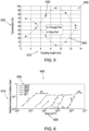
- Figure 5 shows a graph 500 of coupling length and light transmission percentage for an implanted waveguide coupler adjacent to a conventional waveguide in accordance with exemplary embodiments of the present disclosure.
- the Y-axis 520 shows the transmission of light as a percentage of the input power.
- Figure 5 illustrates that, in accordance with embodiments of this disclosure, a change in coupling length 510, corresponding to the length of an implanted waveguide coupler (such as implanted waveguide coupler 340 in Fig. 3 ) adjacent to a conventional waveguide (such as conventional waveguide 330 in Fig. 3 ), affects the transmission 530 of light of the through port (such as through port 410 in Fig.4 ) associated with the conventional waveguide.
- an implanted waveguide coupler such as implanted waveguide coupler 340 in Fig. 3
- a conventional waveguide such as conventional waveguide 330 in Fig. 3
- the transmission of light 540 from a drop port (such as drop port 420 in Fig. 4 ) associated with the implanted waveguide also varies accordingly.
- the graph of Figure 5 illustrates that a short coupling length, equating to an adjacent approximately 3 ⁇ m long implanted waveguide coupler in this example, allows almost 70% of light to couple from a conventional waveguide to the adjacent implanted waveguide coupler.
- This light transmission efficiency reduces as the coupling length of the implanted waveguide coupler increases to approximately 9 ⁇ m, and begins to increase again above this length to a value of approximately 45% light transmission at a coupling length of 13 ⁇ m.
- Figure 6 shows a graph 600 of change in refractive index 610 as a function of ion implant dosage 620 for several implant species 630 implanted into silicon.
- the graph of Figure 6 illustrates that refractive index 610 may vary based on ion implantation dose 620, and based on a variety of ion implant species 630.
- the ion implant species forming the implanted waveguide coupler may include, but is not limited to, Si, Ge, C, Sn, Ne, Ar, Kr, Xe, B, Ga, P, As, Sb or any suitable ion that can be implanted into a material to change the refractive index of said material.
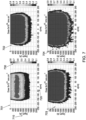
- Figure 7 shows four plots, 701-704, of implant dose variations for 100keV implant energy of Ge into Si.
- the plots show depth of implant species 710 and width 720.
- the scale 730 represents the damage fraction, in which 80% crystal lattice disorder corresponds with a damage fraction of 0.8.
- the refractive index change is dominated by the percentage of lattice damage in this case.
- ion implant species that causes one or more of these changes may be suitable for creating an implanted waveguide coupler.
- ion implantation causes a disordering of the crystal lattice structure of a material, for example the implantation of Si or Ge ions into a silicon photonic circuit material. This disordering is from a more crystalline state to a more amorphous state.
- coupling intensity between an implanted waveguide coupler and a conventional waveguide can be varied by changing the length of the implanted waveguide coupler, or the ion implant species or ion implant dose.
- Other mechanisms to vary coupling intensity may include the size, shape, location, and direction of the implanted waveguide coupler.
- the ion implant species, dosage, implant energy, and direction of ion implantation may also influence the coupling intensity of the implanted waveguide coupler. In this way, the coupling, and the amount of light coupled, can be controlled by controlling one or more of the above variables.
- the coupling mechanism is via evanescent coupling, or butt-coupling, as a result of a change in refractive index of the material into which the ion implanted waveguide coupler is formed.
- the ion implanted waveguide coupler is formed to be erasable, and may be erased by a heating or annealing process, or by further ion implantation. Heating of the implanted region may cause a change in crystal lattice structure, composition, and charge, which may in turn cause a change in refractive index of this region. Similarly, a further implantation of ions into this region may also change the refractive index of this region.
- the ion implantation to form the implanted waveguide coupler causes the refractive index to increase, allowing coupling to an adjacent conventional waveguide.
- the refractive index of the implanted region can reduce, thereby stopping the coupling of photons from, or to, the conventional waveguide.
- further implantation may cause the refractive index to increase further, thereby stopping the coupling to the conventional waveguide.
- the mechanism of erasing the implanted waveguide coupler is through a re-ordering of the crystal lattice structure of a material, for example a silicon photonic circuit material.
- the annealing process causes ordering of the crystal lattice from a more amorphous state to a more crystalline state, which acts to change the refractive index and reduce or stop coupling between an implanted waveguide coupler and conventional waveguide.
- further ion implantation into the implant region of an implanted waveguide coupler causes further disorder of the crystal lattice structure, thereby causing the structure to become more amorphous, and changes the refractive index further. This acts to reduce or stop coupling between an implanted waveguide coupler and conventional waveguide.
- the formation of the implanted optical coupler may be thought of as engaging the coupler to a conventional waveguide, allowing light to be extracted from (or inserted into) the conventional waveguide.
- the implanted optical coupler may then be disengaged from the conventional waveguide, for example by annealing or further implantation, to stop the extraction of light from the conventional waveguide (or input of light to the conventional waveguide).
- FIG 8 illustrates a flow chart 800 of the fabrication steps of forming an implanted waveguide coupler according to an exemplary embodiment of the present disclosure.
- the implanted waveguide coupler may be fabricated on a buried oxide wafer as described above in relation to Figure 3 .
- a mask is deposited onto a wafer forming the photonic circuit structure including at least one conventional waveguide.
- the mask may be a hard mask, such as SiO 2 , or may be a photoresist mask.
- the mask is processed to form at least one opening adjacent to the at least one conventional waveguide.
- the mask is processed using photolithography or e-beam lithography to pattern the mask, and dry or wet chemical etching to form the opening in the mask.
- ions are implanted through the at least one opening, into the wafer forming the photonic circuit structure, adjacent to the at least one waveguide.
- the mask may be removed.
- a test waveguide may be formed.
- the test waveguide may be coupled to the conventional waveguide via the implanted waveguide coupler and evanescent coupling, as illustrated by waveguide 240 of Figure 2 , or may be directly butt-coupled to the implanted waveguide coupler, for example as with the coupler 140 of Figure 1 .
- Test signals may be transmitted in to, or out from, the test waveguide, via the implanted waveguide coupler, into the conventional waveguide for testing a photonic circuit.
- the implanted waveguide coupler may be erased, as outlined above, by an annealing or further implantation process. Therefore during operation of the photonic circuit, light can transmit through the conventional waveguide, without loss due to coupling to the now erased implanted waveguide coupler.
- Figure 9 shows a flow chart of a method 900 of testing the photonic circuit using the implanted coupler and then erasing the coupler.
- light is transmitted or coupled into and/or out of the conventional waveguide via the adjacent coupler waveguide to test the photonic device.
- the coupling between the conventional waveguide is erased or removed, in this case by heating the substrate locally in the implanted region, or by further implanting ions, to remove the coupling to the adjacent implanted waveguide region.
- Figure 10 illustrates an exemplary embodiment 1000 of the present disclosure comprising an array of implanted waveguide couplers, such as one or more of the implanted waveguide couplers 110 of Fig. 1 , and/or 210 of Fig. 2 of the present disclosure.
- Figure 10 illustrates a series of implanted waveguide couplers 1010, 1012, 1014 which can be fabricated alongside one or more conventional waveguides 1030 for example by ion implantation, as described above.
- the design of each implanted waveguide coupler 1010, 1012, 1014 can be similar to the designs shown in Fig. 1 and/or Fig. 2 .
- Each implanted waveguide coupler can couple a percentage of the light power from the conventional waveguide 1030.
- arrow 1020 showing the light in the conventional waveguide 1030
- arrows 1040, 1045 and 1050 showing the coupling of a portion of light 1020 by each of implanted waveguide couplers 1010, 1020, 1030 to an output.
- one or more of the implanted waveguide couplers 1010, 1012, 1014 can be erased, by localized annealing or further ion implantation. Additionally, the portion of light coupled by each implanted waveguide coupler 1010, 1012, 1014 may be changed by annealing or by further ion implantation.
- implanted waveguide coupler 1010 and 1014 may be erased, resulting in more light power 1020 coupling from the conventional waveguide 1030 through implanted waveguide coupler 1012 and to an output or another waveguide or photonic device as light 1045.
- the portion of light coupled by implanted waveguide coupler 1010 may be halved, by annealing or further ion implantation but without completely erasing the implanted waveguide coupler, thereby allowing more light to couple via implanted waveguides 1012 and 1014.
- An array design such as that described above can allow varying of the percentage of light power distributed to different parts of a photonic circuit. This could be used to balance the performance of the whole circuit, or to ensure all of the light power input into a circuit is transmitted to the part or the circuit under test. Regarding wafer-scale testing, this could also enable multiple tests of a photonic circuit to be performed simultaneously.
- the exemplary embodiment of Fig. 10 may be scaled to form a programmable optical circuit. This can be achieved by making a generic circuit containing a number of conventional waveguides 1030 and implanted waveguide couplers 1010, 1012, 1014, and erasing selected ones of the implanted waveguide couplers 1010, 1012, 1014 to obtain any required functionality. This could be particularly useful in switching arrays for example, where only certain switching configurations are allowed. In an example, this could enable a programmable connection between N inputs and M outputs.
- the example of Figure 10 shows a 1x4 photonic switching circuit. Persons of skill in the art will envisage the use of such an embodiment for programming more complex circuits.
- Figure 11a shows an optical microscope image of a fabricated single-stage directional coupler in accordance with the embodiment described above in relation to Figure 1 .
- Figure 11b shows an optical microscope image of a fabricated a dual-stage directional coupler in accordance with the embodiment described above in relation to Figure 2 .
- the degree of transmitted non-coupled light intensity out of the through port and of coupled light out of the drop port were measured following a sequential annealing of the coupling length of the directional coupler using repeated passes of a localised laser annealing system as shown in Figure 12 .
- a localised laser annealing system as shown in Figure 12 .
- an Ar+ laser or another suitable laser is focussed onto the surface of the wafer using a microscope objective to locally heat the surface.
- the stage on which the wafer is placed is then operated so as to move the focussed annealing laser beam sequentially across the end of the ion implanted waveguide to sequentially anneal and erase sections of the ion implanted waveguide to reduce the coupling length Lc of the single and dual stage directional couplers.
- Figure 15a shows an optical microscope image of a fabricated 1 ⁇ 4 photonic switching circuit
- Figure 15b shows an optical microscope image of a fabricated 2 ⁇ 2 photonic switching circuit.
- the 1x4 photonic switching circuit is initially configured to couple a maximum amount of the input light travelling through each coupler to each of the output ports P1, P2, P3 and P4. Measurements of the transmitted light intensity were taken at each of the output ports with the switching circuit in its initial state, and then after its first, second, and third sequential couplers are annealed and erased. The results are shown in Figures 16 a, b, c and d , respectively.
- the 2x2 photonic switching circuit was initially configured with directional couplers so that it operates in cross coupling mode, such that the light input at terminal T1 is coupled across to be output at port P2, and such that the light input at terminal T2 is coupled across to be output at port P1.
- a measurement of operation in this cross coupling mode this can be seen in Figure 17a , which shows that the input light at T1 and T2 is indeed coupled across to the opposing port, P2 and P1 respectively, with the signal difference to the through coupled ports being 18.3dB at 1550nm.
- an external laser source is used to locally heat and anneal the wafer to erase, e.g. selectively, the directional couplers
- other local annealing methods may be suitable.
- the photonic device may be provided with an eraser system configured to heat a region including the ion implanted region to modify the crystal structure of the wafer material in the region to change the refractive index thereof and remove the optical coupling with the adjacent conventional waveguide.
- the eraser system may be provided on the photonic device by a resistive heating element, as shown in Figure 18 .
- the resistive heating element comprises, as shown in the view from the top seen in Figure 18a , a resistive metal heater deposited on the surface of the wafer having metal contacts on each side of the conventional waveguides of the dual stage directional coupler, and a narrowed heating element aligned bridging the conventional waveguides and extending along the surface of the wafer aligned with the ion implanted region providing the coupling waveguide.
- Figure 18b shows in a cross section through the ion implanted region and the neighbouring conventional rib waveguides, the layer of metal on top of the wafer providing the resistive metal heating element.
- the resistive heater may be arranged on the photonic device so as to locally heat and anneal the ion implanted region when an electrical current passes through the resistive heating element.
- the photonic device may be fabricated with a switching mechanism, for example, using a CMOS compatible metal deposition process, to provide a directional coupler erasing system which may be operated in use following testing of the device.
Landscapes
- Physics & Mathematics (AREA)
- Engineering & Computer Science (AREA)
- Optics & Photonics (AREA)
- General Physics & Mathematics (AREA)
- Chemical & Material Sciences (AREA)
- Microelectronics & Electronic Packaging (AREA)
- Analytical Chemistry (AREA)
- Nanotechnology (AREA)
- Mechanical Engineering (AREA)
- Metallurgy (AREA)
- Organic Chemistry (AREA)
- Materials Engineering (AREA)
- Chemical Kinetics & Catalysis (AREA)
- Life Sciences & Earth Sciences (AREA)
- Biophysics (AREA)
- Crystallography & Structural Chemistry (AREA)
- Optical Integrated Circuits (AREA)
Claims (13)
- Verfahren zum Bilden eines löschbaren optischen Kopplers (110, 210) in einer photonischen Vorrichtung, die einen herkömmlichen optischen Wellenleiter (130, 230) umfasst, der in einem kristallinen Wafer (105, 205) gebildet ist, dadurch gekennzeichnet, dass das Verfahren umfasst:
selektives Implantieren von Ionen in einem lokalisierten Bereich des Wafermaterials angrenzend an den herkömmlichen Wellenleiter der photonischen Vorrichtung, um eine Modifikation der Kristallgitterstruktur des ionenimplantierten Bereichs des Wafermaterials und eine Änderung des Brechungsindex in diesem zu bewirken, um dadurch einen ionenimplantierten Wellenleiter zu bilden, der optisch mit dem angrenzenden herkömmlichen Wellenleiter gekoppelt ist, um Licht daraus auszukoppeln oder darin einzukoppeln, wobei das kristalline Wafermaterial und der ionenimplantierte Wellenleiter derart sind, dass die Kristallgitterstruktur oder die Zusammensetzung des Wafermaterials, um die optische Kopplung mit dem herkömmlichen Wellenleiter zu reduzieren oder zu beseitigen, durch weitere Modifikation des Brechungsindex in dem ionenimplantierten Bereich, der den ionenimplantierten Wellenleiter bildet, modifiziert werden kann, wobei die weitere Modifikation des Brechungsindex des ionenimplantierten Bereichs (110, 210) eine zusätzliche Ionenimplantation oder die Anwendung von Wärme umfasst. - Verfahren nach Anspruch 1, ferner umfassend Steuern bei der selektiven Ionenimplantation von einem oder mehreren von Größe, Form oder Ort des lokalisierten Bereichs des Wafermaterials (105, 205), in den Ionen zu implantieren sind, oder der Implantationsrichtung oder der Art, Dosierung oder Energie der implantierten Ionen, um die optische Kopplung zwischen dem herkömmlichen Wellenleiter (130, 230) und dem dadurch gebildeten ionenimplantierten Wellenleiter (110, 210) zu steuern, oder
wobei die Größe, Form oder der Ort des lokalisierten Bereichs, die Implantationsrichtung und die Art, Dosierung und Energie der implantierten Ionen ausgewählt werden, um eine vorbestimmte Größe an optischer Kopplung zwischen dem herkömmlichen Wellenleiter und dem ionenimplantierten Wellenleiter zu erhalten. - Verfahren nach einem vorhergehenden Anspruch, ferner umfassend Durchführen eines Tests der photonischen Vorrichtung durch Koppeln von Licht in den oder aus dem herkömmlichen Wellenleiter (130, 230) durch den ionenimplantierten Wellenleiter (110, 210) und/oder
ferner umfassend Anwenden von Wärme auf den implantierten Bereich, der den ionenimplantierten Wellenleiter bildet, um die Kristallstruktur des Wafermaterials (105, 205) in dem implantierten Bereich zu modifizieren, um dessen Brechungsindex zu ändern und die optische Kopplung mit dem angrenzenden herkömmlichen Wellenleiter zu reduzieren oder zu beseitigen. - Verfahren nach einem vorhergehenden Anspruch,wobei die implantierten Ionen die Kristallgitterstruktur des Wafermaterials von einem stärker geordneten Zustand in einen weniger geordneten Zustand modifizieren und/oderwobei die Anwendung von Wärme auf den ionenimplantierten Wellenleiter (110, 210) die Kristallgitterstruktur darin von einem weniger geordneten Zustand in einen stärker geordneten Zustand ändert.
- Verfahren nach einem vorhergehenden Anspruch, wobei selektives Implantieren der Ionen in dem lokalisierten Bereich des Wafermaterials (105, 205) umfasst:Anordnen (810) eines Maskenmaterials auf der Vorrichtung,Bearbeiten (820) des Maskenmaterials, um mindestens eine Öffnung angrenzend an den herkömmlichen Wellenleiter (130, 230) der photonischen Vorrichtung zu bilden, undImplantieren (830) von Ionen in das Wafermaterial durch die Öffnung der Maske angrenzend an den herkömmlichen Wellenleiter der photonischen Vorrichtung, optional, wobei die Maske umfasst:eine Photoresistschicht; und/odereine Hartmaske, wobei die Hartmaske optional aus SiO2 gebildet ist.
- Verfahren nach Anspruch 5, wobei das Bearbeiten des Maskenmaterials enthält:Strukturieren des Maskenmaterials mit einer photolithografischen oder einer E-Beam-Lithografiemethode; undÄtzen des Maskenmaterials, um die mindestens eine Öffnung der Maske zu bilden.
- Verfahren nach einem vorhergehenden Anspruch, ferner umfassend Bereitstellen eines weiteren herkömmlichen Wellenleiters, der mit dem ionenimplantierten Wellenleiter (110, 210) gekoppelt ist, um Licht in den herkömmlichen Wellenleiter (130, 230) der photonischen Vorrichtung durch den ionenimplantierten Wellenleiter einzukoppeln und aus diesem auszukoppeln.
- Verfahren nach Anspruch 7, wobei das Koppeln von Licht zwischen dem herkömmlichen Wellenleiter, dem ionenimplantierten Wellenleiter und dem weiteren herkömmlichen Wellenleiter über eine evaneszente Kopplung erfolgt.
- Verfahren nach einem vorhergehenden Anspruch, wobei der herkömmliche Wellenleiter (130, 230) als Rippenwellenleiter gebildet ist und/oder
wobei das Wafermaterial (105, 205) Silicium ist. - Verfahren nach einem vorhergehenden Anspruch, umfassend:Bilden des herkömmlichen Wellenleiters (130, 230) als eine Rippenwellenleiterstruktur in dem Wafermaterial;Implantieren der Ionen angrenzend an die Rippenstruktur des herkömmlichen Wellenleiters.
- Vorrichtung, umfassend:ein Substrat, das aus einem Wafermaterial (105, 205) gebildet ist,einen herkömmlichen optischen Wellenleiter (130, 230), der durch das Wafermaterial gebildet ist, undeinen Wellenleiter (110, 210), der vorübergehend in dem Wafermaterial angrenzend an den herkömmlichen optischen Wellenleiter gebildet ist, wobei der vorübergehend gebildete Wellenleiter dazu konfiguriert ist, Licht in den herkömmlichen optischen Wellenleiter einzukoppeln oder aus diesem auszukoppeln,wobei die optische Kopplung zwischen dem vorübergehend gebildeten Wellenleiter und dem herkömmlichen Wellenleiter durch Ändern des Brechungsindex des vorübergehend gebildeten Wellenleiters beseitigbar ist,dadurch gekennzeichnet, dass der vorübergehend gebildete Wellenleiter ein ionenimplantierter Wellenleiter ist, der dazu konfiguriert ist, während eines Tests Licht in den herkömmlichen optischen Wellenleiter einzukoppeln oder aus diesem auszukoppeln,und dadurch, dass das Wafermaterial und der ionenimplantierte Wellenleiter derart sind, dass die optische Kopplung zwischen dem ionenimplantierten Wellenleiter durch zusätzliche Ionenimplantation oder Erwärmen des Wafermaterials beseitigbar ist.
- Vorrichtung nach Anspruch 11, ferner umfassend ein Testsystem, das dazu konfiguriert ist, die Vorrichtung durch Einkoppeln von Licht in den herkömmlichen Wellenleiter (130, 230) oder Auskoppeln von Licht aus diesem durch den ionenimplantierten Wellenleiter (110, 210) zu testen und/oder
ein Löschsystem, das dazu konfiguriert ist, einen Bereich zu erwärmen, der den ionenimplantierten Wellenleiter enthält, um die Kristallstruktur des Wafermaterials in dem Bereich zu modifizieren, um dessen Brechungsindex zu ändern und die optische Kopplung mit dem angrenzenden herkömmlichen Wellenleiter zu beseitigen. - Vorrichtung nach einem der Ansprüche 11 bis 12, wobei der herkömmliche Lichtwellenleiter (130, 230) als ein Rippenwellenleiter gebildet ist und/oder
wobei die Vorrichtung ferner einen weiteren herkömmlichen Wellenleiter umfasst, der mit dem ionenimplantierten Wellenleiter gekoppelt ist, um Licht in den herkömmlichen Wellenleiter der photonischen Vorrichtung durch den ionenimplantierten Wellenleiter einzukoppeln oder aus diesem auszukoppeln.
Applications Claiming Priority (2)
| Application Number | Priority Date | Filing Date | Title |
|---|---|---|---|
| GB1704690.5A GB2561155A (en) | 2017-03-24 | 2017-03-24 | Erasable coupler |
| PCT/GB2018/050651 WO2018172740A1 (en) | 2017-03-24 | 2018-03-14 | Erasable optical coupler |
Publications (2)
| Publication Number | Publication Date |
|---|---|
| EP3602153A1 EP3602153A1 (de) | 2020-02-05 |
| EP3602153B1 true EP3602153B1 (de) | 2023-06-21 |
Family
ID=58688172
Family Applications (1)
| Application Number | Title | Priority Date | Filing Date |
|---|---|---|---|
| EP18714025.6A Active EP3602153B1 (de) | 2017-03-24 | 2018-03-14 | Löschbarer optischer koppler |
Country Status (4)
| Country | Link |
|---|---|
| US (1) | US11209593B2 (de) |
| EP (1) | EP3602153B1 (de) |
| GB (1) | GB2561155A (de) |
| WO (1) | WO2018172740A1 (de) |
Families Citing this family (1)
| Publication number | Priority date | Publication date | Assignee | Title |
|---|---|---|---|---|
| US11175451B2 (en) * | 2019-09-26 | 2021-11-16 | Intel Corporation | Mechanisms for refractive index tuning semiconductor photonic devices |
Family Cites Families (8)
| Publication number | Priority date | Publication date | Assignee | Title |
|---|---|---|---|---|
| JPS59121307A (ja) * | 1982-12-21 | 1984-07-13 | Fujitsu Ltd | 光モニタ方式 |
| US6819845B2 (en) * | 2001-08-02 | 2004-11-16 | Ultradots, Inc. | Optical devices with engineered nonlinear nanocomposite materials |
| US6957007B2 (en) * | 2002-07-29 | 2005-10-18 | General Electric Company | Method and apparatus for fabricating waveguides and waveguides fabricated therefrom |
| JP3937218B2 (ja) * | 2002-10-01 | 2007-06-27 | 日本電信電話株式会社 | プログラマブル光回路 |
| WO2006106524A2 (en) * | 2005-04-07 | 2006-10-12 | Yissum Research Development Company Of The Hebrew University Of Jerusalem | Amorphous and crystalline potassium lithium tantalate niobate (kltn) structures for optical and electro-optic devices |
| US8380027B2 (en) * | 2010-05-10 | 2013-02-19 | Intel Corporation | Erasable ion implanted optical couplers |
| US9575250B2 (en) * | 2014-07-03 | 2017-02-21 | Empire Technology Development Llc | Direct writable and erasable waveguides in optoelectronic systems |
| US11175451B2 (en) * | 2019-09-26 | 2021-11-16 | Intel Corporation | Mechanisms for refractive index tuning semiconductor photonic devices |
-
2017
- 2017-03-24 GB GB1704690.5A patent/GB2561155A/en not_active Withdrawn
-
2018
- 2018-03-14 EP EP18714025.6A patent/EP3602153B1/de active Active
- 2018-03-14 WO PCT/GB2018/050651 patent/WO2018172740A1/en not_active Ceased
-
2019
- 2019-09-24 US US16/580,298 patent/US11209593B2/en active Active
Non-Patent Citations (1)
| Title |
|---|
| ROBERTS A ET AL: "Fabrication of Buried Channel Waveguides in Fused Silica Using Focused MeV Proton Beam Irradiation", JOURNAL OF LIGHTWAVE TECHNOLOGY, IEEE, USA, vol. 14, no. 11, 1 November 1996 (1996-11-01), XP011028702, ISSN: 0733-8724 * |
Also Published As
| Publication number | Publication date |
|---|---|
| WO2018172740A1 (en) | 2018-09-27 |
| EP3602153A1 (de) | 2020-02-05 |
| GB2561155A (en) | 2018-10-10 |
| US11209593B2 (en) | 2021-12-28 |
| US20200088943A1 (en) | 2020-03-19 |
| GB201704690D0 (en) | 2017-05-10 |
Similar Documents
| Publication | Publication Date | Title |
|---|---|---|
| CN102893189B (zh) | 可擦除的离子注入的光耦合器 | |
| CN100495094C (zh) | 在soi光学平台上形成的亚微米平面光波设备 | |
| TW563272B (en) | Optical network for actuation of switches in a reconfigurable antenna | |
| KR101412864B1 (ko) | 광 도파관 격자 커플러 | |
| US11360272B2 (en) | Wafer-scale-integrated silicon-photonics-based optical switching system and method of forming | |
| US9472710B1 (en) | Low-loss large-grain optical waveguide for interconnecting components integrated on a glass substrate | |
| US11662519B2 (en) | Optical waveguide tuning element | |
| EP3602153B1 (de) | Löschbarer optischer koppler | |
| EP1623255A2 (de) | Verlustarme, ausserebene wellenleiter verwendende lichtwellenleiterbrücke | |
| Tyler et al. | SiN Integrated Photonics for near-infrared LIDAR | |
| TW202449442A (zh) | 包含相變材料之可調式晶片上可變比例光學耦合器 | |
| US6650819B1 (en) | Methods for forming separately optimized waveguide structures in optical materials | |
| US11803011B1 (en) | Optical switch having latched switch states and associated methods | |
| US11982883B2 (en) | Optical device having phase change material and associated methods | |
| KR100281736B1 (ko) | 와이-분기형 광도파로 편광 분리기의 구조 및 제작방법 | |
| Herben et al. | Ultra-compact polarisation independent PHASAR demultiplexer | |
| Chu et al. | Silicon photonic-wire waveguide devices | |
| JP2004126088A (ja) | プログラマブル光回路 | |
| US20050051514A1 (en) | Fabrication of optical components using Si, SiGe, SiGeC, and chemical endpoint detection | |
| WO2025165376A2 (en) | Integrated microlens coupler for photonic integrated circuits | |
| HK40057673A (en) | Optical waveguide tuning element | |
| Teo et al. | Three dimensional integration of waveguides in bulk silicon | |
| UB | D4. 3: Fabrication, characterization and system-level evaluation of a 4x4 thermooptic DLSPP-based switching matrix | |
| Wang et al. | Silicon on Silicon Carbide Ring Resonators for Coupling to Color Centers | |
| JP2005215200A (ja) | 光集積回路の作製方法 |
Legal Events
| Date | Code | Title | Description |
|---|---|---|---|
| STAA | Information on the status of an ep patent application or granted ep patent |
Free format text: STATUS: UNKNOWN |
|
| STAA | Information on the status of an ep patent application or granted ep patent |
Free format text: STATUS: THE INTERNATIONAL PUBLICATION HAS BEEN MADE |
|
| PUAI | Public reference made under article 153(3) epc to a published international application that has entered the european phase |
Free format text: ORIGINAL CODE: 0009012 |
|
| STAA | Information on the status of an ep patent application or granted ep patent |
Free format text: STATUS: REQUEST FOR EXAMINATION WAS MADE |
|
| 17P | Request for examination filed |
Effective date: 20191023 |
|
| AK | Designated contracting states |
Kind code of ref document: A1 Designated state(s): AL AT BE BG CH CY CZ DE DK EE ES FI FR GB GR HR HU IE IS IT LI LT LU LV MC MK MT NL NO PL PT RO RS SE SI SK SM TR |
|
| AX | Request for extension of the european patent |
Extension state: BA ME |
|
| DAV | Request for validation of the european patent (deleted) | ||
| DAX | Request for extension of the european patent (deleted) | ||
| STAA | Information on the status of an ep patent application or granted ep patent |
Free format text: STATUS: EXAMINATION IS IN PROGRESS |
|
| 17Q | First examination report despatched |
Effective date: 20201111 |
|
| GRAP | Despatch of communication of intention to grant a patent |
Free format text: ORIGINAL CODE: EPIDOSNIGR1 |
|
| STAA | Information on the status of an ep patent application or granted ep patent |
Free format text: STATUS: GRANT OF PATENT IS INTENDED |
|
| INTG | Intention to grant announced |
Effective date: 20221214 |
|
| GRAS | Grant fee paid |
Free format text: ORIGINAL CODE: EPIDOSNIGR3 |
|
| GRAA | (expected) grant |
Free format text: ORIGINAL CODE: 0009210 |
|
| STAA | Information on the status of an ep patent application or granted ep patent |
Free format text: STATUS: THE PATENT HAS BEEN GRANTED |
|
| RAP3 | Party data changed (applicant data changed or rights of an application transferred) |
Owner name: UNIVERSITY OF SOUTHAMPTON |
|
| AK | Designated contracting states |
Kind code of ref document: B1 Designated state(s): AL AT BE BG CH CY CZ DE DK EE ES FI FR GB GR HR HU IE IS IT LI LT LU LV MC MK MT NL NO PL PT RO RS SE SI SK SM TR |
|
| REG | Reference to a national code |
Ref country code: CH Ref legal event code: EP |
|
| REG | Reference to a national code |
Ref country code: DE Ref legal event code: R096 Ref document number: 602018052074 Country of ref document: DE |
|
| REG | Reference to a national code |
Ref country code: AT Ref legal event code: REF Ref document number: 1581301 Country of ref document: AT Kind code of ref document: T Effective date: 20230715 |
|
| REG | Reference to a national code |
Ref country code: IE Ref legal event code: FG4D |
|
| REG | Reference to a national code |
Ref country code: LT Ref legal event code: MG9D |
|
| REG | Reference to a national code |
Ref country code: NL Ref legal event code: MP Effective date: 20230621 |
|
| PG25 | Lapsed in a contracting state [announced via postgrant information from national office to epo] |
Ref country code: SE Free format text: LAPSE BECAUSE OF FAILURE TO SUBMIT A TRANSLATION OF THE DESCRIPTION OR TO PAY THE FEE WITHIN THE PRESCRIBED TIME-LIMIT Effective date: 20230621 Ref country code: NO Free format text: LAPSE BECAUSE OF FAILURE TO SUBMIT A TRANSLATION OF THE DESCRIPTION OR TO PAY THE FEE WITHIN THE PRESCRIBED TIME-LIMIT Effective date: 20230921 |
|
| REG | Reference to a national code |
Ref country code: AT Ref legal event code: MK05 Ref document number: 1581301 Country of ref document: AT Kind code of ref document: T Effective date: 20230621 |
|
| PG25 | Lapsed in a contracting state [announced via postgrant information from national office to epo] |
Ref country code: RS Free format text: LAPSE BECAUSE OF FAILURE TO SUBMIT A TRANSLATION OF THE DESCRIPTION OR TO PAY THE FEE WITHIN THE PRESCRIBED TIME-LIMIT Effective date: 20230621 Ref country code: NL Free format text: LAPSE BECAUSE OF FAILURE TO SUBMIT A TRANSLATION OF THE DESCRIPTION OR TO PAY THE FEE WITHIN THE PRESCRIBED TIME-LIMIT Effective date: 20230621 Ref country code: LV Free format text: LAPSE BECAUSE OF FAILURE TO SUBMIT A TRANSLATION OF THE DESCRIPTION OR TO PAY THE FEE WITHIN THE PRESCRIBED TIME-LIMIT Effective date: 20230621 Ref country code: LT Free format text: LAPSE BECAUSE OF FAILURE TO SUBMIT A TRANSLATION OF THE DESCRIPTION OR TO PAY THE FEE WITHIN THE PRESCRIBED TIME-LIMIT Effective date: 20230621 Ref country code: HR Free format text: LAPSE BECAUSE OF FAILURE TO SUBMIT A TRANSLATION OF THE DESCRIPTION OR TO PAY THE FEE WITHIN THE PRESCRIBED TIME-LIMIT Effective date: 20230621 Ref country code: GR Free format text: LAPSE BECAUSE OF FAILURE TO SUBMIT A TRANSLATION OF THE DESCRIPTION OR TO PAY THE FEE WITHIN THE PRESCRIBED TIME-LIMIT Effective date: 20230922 |
|
| PG25 | Lapsed in a contracting state [announced via postgrant information from national office to epo] |
Ref country code: FI Free format text: LAPSE BECAUSE OF FAILURE TO SUBMIT A TRANSLATION OF THE DESCRIPTION OR TO PAY THE FEE WITHIN THE PRESCRIBED TIME-LIMIT Effective date: 20230621 |
|
| PG25 | Lapsed in a contracting state [announced via postgrant information from national office to epo] |
Ref country code: SK Free format text: LAPSE BECAUSE OF FAILURE TO SUBMIT A TRANSLATION OF THE DESCRIPTION OR TO PAY THE FEE WITHIN THE PRESCRIBED TIME-LIMIT Effective date: 20230621 |
|
| PG25 | Lapsed in a contracting state [announced via postgrant information from national office to epo] |
Ref country code: ES Free format text: LAPSE BECAUSE OF FAILURE TO SUBMIT A TRANSLATION OF THE DESCRIPTION OR TO PAY THE FEE WITHIN THE PRESCRIBED TIME-LIMIT Effective date: 20230621 |
|
| PG25 | Lapsed in a contracting state [announced via postgrant information from national office to epo] |
Ref country code: IS Free format text: LAPSE BECAUSE OF FAILURE TO SUBMIT A TRANSLATION OF THE DESCRIPTION OR TO PAY THE FEE WITHIN THE PRESCRIBED TIME-LIMIT Effective date: 20231021 |
|
| PG25 | Lapsed in a contracting state [announced via postgrant information from national office to epo] |
Ref country code: SM Free format text: LAPSE BECAUSE OF FAILURE TO SUBMIT A TRANSLATION OF THE DESCRIPTION OR TO PAY THE FEE WITHIN THE PRESCRIBED TIME-LIMIT Effective date: 20230621 Ref country code: SK Free format text: LAPSE BECAUSE OF FAILURE TO SUBMIT A TRANSLATION OF THE DESCRIPTION OR TO PAY THE FEE WITHIN THE PRESCRIBED TIME-LIMIT Effective date: 20230621 Ref country code: RO Free format text: LAPSE BECAUSE OF FAILURE TO SUBMIT A TRANSLATION OF THE DESCRIPTION OR TO PAY THE FEE WITHIN THE PRESCRIBED TIME-LIMIT Effective date: 20230621 Ref country code: PT Free format text: LAPSE BECAUSE OF FAILURE TO SUBMIT A TRANSLATION OF THE DESCRIPTION OR TO PAY THE FEE WITHIN THE PRESCRIBED TIME-LIMIT Effective date: 20231023 Ref country code: IS Free format text: LAPSE BECAUSE OF FAILURE TO SUBMIT A TRANSLATION OF THE DESCRIPTION OR TO PAY THE FEE WITHIN THE PRESCRIBED TIME-LIMIT Effective date: 20231021 Ref country code: ES Free format text: LAPSE BECAUSE OF FAILURE TO SUBMIT A TRANSLATION OF THE DESCRIPTION OR TO PAY THE FEE WITHIN THE PRESCRIBED TIME-LIMIT Effective date: 20230621 Ref country code: EE Free format text: LAPSE BECAUSE OF FAILURE TO SUBMIT A TRANSLATION OF THE DESCRIPTION OR TO PAY THE FEE WITHIN THE PRESCRIBED TIME-LIMIT Effective date: 20230621 Ref country code: CZ Free format text: LAPSE BECAUSE OF FAILURE TO SUBMIT A TRANSLATION OF THE DESCRIPTION OR TO PAY THE FEE WITHIN THE PRESCRIBED TIME-LIMIT Effective date: 20230621 Ref country code: AT Free format text: LAPSE BECAUSE OF FAILURE TO SUBMIT A TRANSLATION OF THE DESCRIPTION OR TO PAY THE FEE WITHIN THE PRESCRIBED TIME-LIMIT Effective date: 20230621 |
|
| PG25 | Lapsed in a contracting state [announced via postgrant information from national office to epo] |
Ref country code: PL Free format text: LAPSE BECAUSE OF FAILURE TO SUBMIT A TRANSLATION OF THE DESCRIPTION OR TO PAY THE FEE WITHIN THE PRESCRIBED TIME-LIMIT Effective date: 20230621 |
|
| REG | Reference to a national code |
Ref country code: DE Ref legal event code: R097 Ref document number: 602018052074 Country of ref document: DE |
|
| PLBE | No opposition filed within time limit |
Free format text: ORIGINAL CODE: 0009261 |
|
| STAA | Information on the status of an ep patent application or granted ep patent |
Free format text: STATUS: NO OPPOSITION FILED WITHIN TIME LIMIT |
|
| PG25 | Lapsed in a contracting state [announced via postgrant information from national office to epo] |
Ref country code: DK Free format text: LAPSE BECAUSE OF FAILURE TO SUBMIT A TRANSLATION OF THE DESCRIPTION OR TO PAY THE FEE WITHIN THE PRESCRIBED TIME-LIMIT Effective date: 20230621 |
|
| PG25 | Lapsed in a contracting state [announced via postgrant information from national office to epo] |
Ref country code: SI Free format text: LAPSE BECAUSE OF FAILURE TO SUBMIT A TRANSLATION OF THE DESCRIPTION OR TO PAY THE FEE WITHIN THE PRESCRIBED TIME-LIMIT Effective date: 20230621 |
|
| 26N | No opposition filed |
Effective date: 20240322 |
|
| PG25 | Lapsed in a contracting state [announced via postgrant information from national office to epo] |
Ref country code: SI Free format text: LAPSE BECAUSE OF FAILURE TO SUBMIT A TRANSLATION OF THE DESCRIPTION OR TO PAY THE FEE WITHIN THE PRESCRIBED TIME-LIMIT Effective date: 20230621 Ref country code: IT Free format text: LAPSE BECAUSE OF FAILURE TO SUBMIT A TRANSLATION OF THE DESCRIPTION OR TO PAY THE FEE WITHIN THE PRESCRIBED TIME-LIMIT Effective date: 20230621 |
|
| REG | Reference to a national code |
Ref country code: CH Ref legal event code: PL |
|
| PG25 | Lapsed in a contracting state [announced via postgrant information from national office to epo] |
Ref country code: BG Free format text: LAPSE BECAUSE OF FAILURE TO SUBMIT A TRANSLATION OF THE DESCRIPTION OR TO PAY THE FEE WITHIN THE PRESCRIBED TIME-LIMIT Effective date: 20230621 |
|
| PG25 | Lapsed in a contracting state [announced via postgrant information from national office to epo] |
Ref country code: LU Free format text: LAPSE BECAUSE OF NON-PAYMENT OF DUE FEES Effective date: 20240314 |
|
| PG25 | Lapsed in a contracting state [announced via postgrant information from national office to epo] |
Ref country code: MC Free format text: LAPSE BECAUSE OF FAILURE TO SUBMIT A TRANSLATION OF THE DESCRIPTION OR TO PAY THE FEE WITHIN THE PRESCRIBED TIME-LIMIT Effective date: 20230621 |
|
| PG25 | Lapsed in a contracting state [announced via postgrant information from national office to epo] |
Ref country code: MC Free format text: LAPSE BECAUSE OF FAILURE TO SUBMIT A TRANSLATION OF THE DESCRIPTION OR TO PAY THE FEE WITHIN THE PRESCRIBED TIME-LIMIT Effective date: 20230621 Ref country code: BG Free format text: LAPSE BECAUSE OF FAILURE TO SUBMIT A TRANSLATION OF THE DESCRIPTION OR TO PAY THE FEE WITHIN THE PRESCRIBED TIME-LIMIT Effective date: 20230621 Ref country code: LU Free format text: LAPSE BECAUSE OF NON-PAYMENT OF DUE FEES Effective date: 20240314 |
|
| REG | Reference to a national code |
Ref country code: BE Ref legal event code: MM Effective date: 20240331 |
|
| PG25 | Lapsed in a contracting state [announced via postgrant information from national office to epo] |
Ref country code: BE Free format text: LAPSE BECAUSE OF NON-PAYMENT OF DUE FEES Effective date: 20240331 |
|
| PG25 | Lapsed in a contracting state [announced via postgrant information from national office to epo] |
Ref country code: IE Free format text: LAPSE BECAUSE OF NON-PAYMENT OF DUE FEES Effective date: 20240314 |
|
| PG25 | Lapsed in a contracting state [announced via postgrant information from national office to epo] |
Ref country code: IE Free format text: LAPSE BECAUSE OF NON-PAYMENT OF DUE FEES Effective date: 20240314 Ref country code: BE Free format text: LAPSE BECAUSE OF NON-PAYMENT OF DUE FEES Effective date: 20240331 Ref country code: CH Free format text: LAPSE BECAUSE OF NON-PAYMENT OF DUE FEES Effective date: 20240331 |
|
| PG25 | Lapsed in a contracting state [announced via postgrant information from national office to epo] |
Ref country code: CY Free format text: LAPSE BECAUSE OF FAILURE TO SUBMIT A TRANSLATION OF THE DESCRIPTION OR TO PAY THE FEE WITHIN THE PRESCRIBED TIME-LIMIT; INVALID AB INITIO Effective date: 20180314 |
|
| PG25 | Lapsed in a contracting state [announced via postgrant information from national office to epo] |
Ref country code: HU Free format text: LAPSE BECAUSE OF FAILURE TO SUBMIT A TRANSLATION OF THE DESCRIPTION OR TO PAY THE FEE WITHIN THE PRESCRIBED TIME-LIMIT; INVALID AB INITIO Effective date: 20180314 |
|
| PGFP | Annual fee paid to national office [announced via postgrant information from national office to epo] |
Ref country code: GB Payment date: 20250929 Year of fee payment: 8 |
|
| PGFP | Annual fee paid to national office [announced via postgrant information from national office to epo] |
Ref country code: FR Payment date: 20250929 Year of fee payment: 8 |
|
| PG25 | Lapsed in a contracting state [announced via postgrant information from national office to epo] |
Ref country code: TR Free format text: LAPSE BECAUSE OF FAILURE TO SUBMIT A TRANSLATION OF THE DESCRIPTION OR TO PAY THE FEE WITHIN THE PRESCRIBED TIME-LIMIT Effective date: 20230621 |
|
| PGFP | Annual fee paid to national office [announced via postgrant information from national office to epo] |
Ref country code: DE Payment date: 20250929 Year of fee payment: 8 |