EP3601480B1 - Method for increasing the light output of microled devices using quantum dots - Google Patents
Method for increasing the light output of microled devices using quantum dots Download PDFInfo
- Publication number
- EP3601480B1 EP3601480B1 EP18718049.2A EP18718049A EP3601480B1 EP 3601480 B1 EP3601480 B1 EP 3601480B1 EP 18718049 A EP18718049 A EP 18718049A EP 3601480 B1 EP3601480 B1 EP 3601480B1
- Authority
- EP
- European Patent Office
- Prior art keywords
- beam splitter
- layer
- illumination device
- light
- layers
- Prior art date
- Legal status (The legal status is an assumption and is not a legal conclusion. Google has not performed a legal analysis and makes no representation as to the accuracy of the status listed.)
- Active
Links
Images


Classifications
-
- C—CHEMISTRY; METALLURGY
- C09—DYES; PAINTS; POLISHES; NATURAL RESINS; ADHESIVES; COMPOSITIONS NOT OTHERWISE PROVIDED FOR; APPLICATIONS OF MATERIALS NOT OTHERWISE PROVIDED FOR
- C09K—MATERIALS FOR MISCELLANEOUS APPLICATIONS, NOT PROVIDED FOR ELSEWHERE
- C09K11/00—Luminescent, e.g. electroluminescent, chemiluminescent materials
- C09K11/02—Use of particular materials as binders, particle coatings or suspension media therefor
- C09K11/025—Use of particular materials as binders, particle coatings or suspension media therefor non-luminescent particle coatings or suspension media
-
- C—CHEMISTRY; METALLURGY
- C09—DYES; PAINTS; POLISHES; NATURAL RESINS; ADHESIVES; COMPOSITIONS NOT OTHERWISE PROVIDED FOR; APPLICATIONS OF MATERIALS NOT OTHERWISE PROVIDED FOR
- C09K—MATERIALS FOR MISCELLANEOUS APPLICATIONS, NOT PROVIDED FOR ELSEWHERE
- C09K11/00—Luminescent, e.g. electroluminescent, chemiluminescent materials
- C09K11/08—Luminescent, e.g. electroluminescent, chemiluminescent materials containing inorganic luminescent materials
- C09K11/88—Luminescent, e.g. electroluminescent, chemiluminescent materials containing inorganic luminescent materials containing selenium, tellurium or unspecified chalcogen elements
- C09K11/881—Chalcogenides
- C09K11/883—Chalcogenides with zinc or cadmium
-
- F—MECHANICAL ENGINEERING; LIGHTING; HEATING; WEAPONS; BLASTING
- F21—LIGHTING
- F21V—FUNCTIONAL FEATURES OR DETAILS OF LIGHTING DEVICES OR SYSTEMS THEREOF; STRUCTURAL COMBINATIONS OF LIGHTING DEVICES WITH OTHER ARTICLES, NOT OTHERWISE PROVIDED FOR
- F21V9/00—Elements for modifying spectral properties, polarisation or intensity of the light emitted, e.g. filters
- F21V9/20—Dichroic filters, i.e. devices operating on the principle of wave interference to pass specific ranges of wavelengths while cancelling others
-
- H—ELECTRICITY
- H01—ELECTRIC ELEMENTS
- H01L—SEMICONDUCTOR DEVICES NOT COVERED BY CLASS H10
- H01L23/00—Details of semiconductor or other solid state devices
- H01L23/52—Arrangements for conducting electric current within the device in operation from one component to another, i.e. interconnections, e.g. wires, lead frames
- H01L23/538—Arrangements for conducting electric current within the device in operation from one component to another, i.e. interconnections, e.g. wires, lead frames the interconnection structure between a plurality of semiconductor chips being formed on, or in, insulating substrates
- H01L23/5387—Flexible insulating substrates
-
- H—ELECTRICITY
- H01—ELECTRIC ELEMENTS
- H01L—SEMICONDUCTOR DEVICES NOT COVERED BY CLASS H10
- H01L25/00—Assemblies consisting of a plurality of semiconductor or other solid state devices
- H01L25/03—Assemblies consisting of a plurality of semiconductor or other solid state devices all the devices being of a type provided for in a single subclass of subclasses H10B, H10D, H10F, H10H, H10K or H10N, e.g. assemblies of rectifier diodes
- H01L25/04—Assemblies consisting of a plurality of semiconductor or other solid state devices all the devices being of a type provided for in a single subclass of subclasses H10B, H10D, H10F, H10H, H10K or H10N, e.g. assemblies of rectifier diodes the devices not having separate containers
- H01L25/075—Assemblies consisting of a plurality of semiconductor or other solid state devices all the devices being of a type provided for in a single subclass of subclasses H10B, H10D, H10F, H10H, H10K or H10N, e.g. assemblies of rectifier diodes the devices not having separate containers the devices being of a type provided for in group H10H20/00
- H01L25/0753—Assemblies consisting of a plurality of semiconductor or other solid state devices all the devices being of a type provided for in a single subclass of subclasses H10B, H10D, H10F, H10H, H10K or H10N, e.g. assemblies of rectifier diodes the devices not having separate containers the devices being of a type provided for in group H10H20/00 the devices being arranged next to each other
-
- H—ELECTRICITY
- H05—ELECTRIC TECHNIQUES NOT OTHERWISE PROVIDED FOR
- H05B—ELECTRIC HEATING; ELECTRIC LIGHT SOURCES NOT OTHERWISE PROVIDED FOR; CIRCUIT ARRANGEMENTS FOR ELECTRIC LIGHT SOURCES, IN GENERAL
- H05B33/00—Electroluminescent light sources
- H05B33/12—Light sources with substantially two-dimensional radiating surfaces
- H05B33/14—Light sources with substantially two-dimensional radiating surfaces characterised by the chemical or physical composition or the arrangement of the electroluminescent material, or by the simultaneous addition of the electroluminescent material in or onto the light source
-
- H—ELECTRICITY
- H10—SEMICONDUCTOR DEVICES; ELECTRIC SOLID-STATE DEVICES NOT OTHERWISE PROVIDED FOR
- H10H—INORGANIC LIGHT-EMITTING SEMICONDUCTOR DEVICES HAVING POTENTIAL BARRIERS
- H10H20/00—Individual inorganic light-emitting semiconductor devices having potential barriers, e.g. light-emitting diodes [LED]
- H10H20/80—Constructional details
- H10H20/81—Bodies
- H10H20/811—Bodies having quantum effect structures or superlattices, e.g. tunnel junctions
- H10H20/812—Bodies having quantum effect structures or superlattices, e.g. tunnel junctions within the light-emitting regions, e.g. having quantum confinement structures
-
- H—ELECTRICITY
- H10—SEMICONDUCTOR DEVICES; ELECTRIC SOLID-STATE DEVICES NOT OTHERWISE PROVIDED FOR
- H10H—INORGANIC LIGHT-EMITTING SEMICONDUCTOR DEVICES HAVING POTENTIAL BARRIERS
- H10H20/00—Individual inorganic light-emitting semiconductor devices having potential barriers, e.g. light-emitting diodes [LED]
- H10H20/80—Constructional details
- H10H20/81—Bodies
- H10H20/816—Bodies having carrier transport control structures, e.g. highly-doped semiconductor layers or current-blocking structures
-
- H—ELECTRICITY
- H10—SEMICONDUCTOR DEVICES; ELECTRIC SOLID-STATE DEVICES NOT OTHERWISE PROVIDED FOR
- H10H—INORGANIC LIGHT-EMITTING SEMICONDUCTOR DEVICES HAVING POTENTIAL BARRIERS
- H10H20/00—Individual inorganic light-emitting semiconductor devices having potential barriers, e.g. light-emitting diodes [LED]
- H10H20/80—Constructional details
- H10H20/85—Packages
- H10H20/855—Optical field-shaping means, e.g. lenses
- H10H20/856—Reflecting means
-
- B—PERFORMING OPERATIONS; TRANSPORTING
- B82—NANOTECHNOLOGY
- B82Y—SPECIFIC USES OR APPLICATIONS OF NANOSTRUCTURES; MEASUREMENT OR ANALYSIS OF NANOSTRUCTURES; MANUFACTURE OR TREATMENT OF NANOSTRUCTURES
- B82Y20/00—Nanooptics, e.g. quantum optics or photonic crystals
-
- B—PERFORMING OPERATIONS; TRANSPORTING
- B82—NANOTECHNOLOGY
- B82Y—SPECIFIC USES OR APPLICATIONS OF NANOSTRUCTURES; MEASUREMENT OR ANALYSIS OF NANOSTRUCTURES; MANUFACTURE OR TREATMENT OF NANOSTRUCTURES
- B82Y40/00—Manufacture or treatment of nanostructures
-
- H—ELECTRICITY
- H10—SEMICONDUCTOR DEVICES; ELECTRIC SOLID-STATE DEVICES NOT OTHERWISE PROVIDED FOR
- H10H—INORGANIC LIGHT-EMITTING SEMICONDUCTOR DEVICES HAVING POTENTIAL BARRIERS
- H10H20/00—Individual inorganic light-emitting semiconductor devices having potential barriers, e.g. light-emitting diodes [LED]
- H10H20/01—Manufacture or treatment
- H10H20/036—Manufacture or treatment of packages
- H10H20/0361—Manufacture or treatment of packages of wavelength conversion means
-
- H—ELECTRICITY
- H10—SEMICONDUCTOR DEVICES; ELECTRIC SOLID-STATE DEVICES NOT OTHERWISE PROVIDED FOR
- H10H—INORGANIC LIGHT-EMITTING SEMICONDUCTOR DEVICES HAVING POTENTIAL BARRIERS
- H10H20/00—Individual inorganic light-emitting semiconductor devices having potential barriers, e.g. light-emitting diodes [LED]
- H10H20/01—Manufacture or treatment
- H10H20/036—Manufacture or treatment of packages
- H10H20/0363—Manufacture or treatment of packages of optical field-shaping means
-
- H—ELECTRICITY
- H10—SEMICONDUCTOR DEVICES; ELECTRIC SOLID-STATE DEVICES NOT OTHERWISE PROVIDED FOR
- H10H—INORGANIC LIGHT-EMITTING SEMICONDUCTOR DEVICES HAVING POTENTIAL BARRIERS
- H10H20/00—Individual inorganic light-emitting semiconductor devices having potential barriers, e.g. light-emitting diodes [LED]
- H10H20/80—Constructional details
- H10H20/84—Coatings, e.g. passivation layers or antireflective coatings
-
- H—ELECTRICITY
- H10—SEMICONDUCTOR DEVICES; ELECTRIC SOLID-STATE DEVICES NOT OTHERWISE PROVIDED FOR
- H10H—INORGANIC LIGHT-EMITTING SEMICONDUCTOR DEVICES HAVING POTENTIAL BARRIERS
- H10H20/00—Individual inorganic light-emitting semiconductor devices having potential barriers, e.g. light-emitting diodes [LED]
- H10H20/80—Constructional details
- H10H20/85—Packages
- H10H20/851—Wavelength conversion means
- H10H20/8511—Wavelength conversion means characterised by their material, e.g. binder
- H10H20/8512—Wavelength conversion materials
-
- H—ELECTRICITY
- H10—SEMICONDUCTOR DEVICES; ELECTRIC SOLID-STATE DEVICES NOT OTHERWISE PROVIDED FOR
- H10H—INORGANIC LIGHT-EMITTING SEMICONDUCTOR DEVICES HAVING POTENTIAL BARRIERS
- H10H20/00—Individual inorganic light-emitting semiconductor devices having potential barriers, e.g. light-emitting diodes [LED]
- H10H20/80—Constructional details
- H10H20/85—Packages
- H10H20/851—Wavelength conversion means
- H10H20/8515—Wavelength conversion means not being in contact with the bodies
-
- H—ELECTRICITY
- H10—SEMICONDUCTOR DEVICES; ELECTRIC SOLID-STATE DEVICES NOT OTHERWISE PROVIDED FOR
- H10H—INORGANIC LIGHT-EMITTING SEMICONDUCTOR DEVICES HAVING POTENTIAL BARRIERS
- H10H20/00—Individual inorganic light-emitting semiconductor devices having potential barriers, e.g. light-emitting diodes [LED]
- H10H20/80—Constructional details
- H10H20/872—Periodic patterns for optical field-shaping, e.g. photonic bandgap structures
-
- Y—GENERAL TAGGING OF NEW TECHNOLOGICAL DEVELOPMENTS; GENERAL TAGGING OF CROSS-SECTIONAL TECHNOLOGIES SPANNING OVER SEVERAL SECTIONS OF THE IPC; TECHNICAL SUBJECTS COVERED BY FORMER USPC CROSS-REFERENCE ART COLLECTIONS [XRACs] AND DIGESTS
- Y10—TECHNICAL SUBJECTS COVERED BY FORMER USPC
- Y10S—TECHNICAL SUBJECTS COVERED BY FORMER USPC CROSS-REFERENCE ART COLLECTIONS [XRACs] AND DIGESTS
- Y10S977/00—Nanotechnology
- Y10S977/70—Nanostructure
- Y10S977/773—Nanoparticle, i.e. structure having three dimensions of 100 nm or less
- Y10S977/774—Exhibiting three-dimensional carrier confinement, e.g. quantum dots
-
- Y—GENERAL TAGGING OF NEW TECHNOLOGICAL DEVELOPMENTS; GENERAL TAGGING OF CROSS-SECTIONAL TECHNOLOGIES SPANNING OVER SEVERAL SECTIONS OF THE IPC; TECHNICAL SUBJECTS COVERED BY FORMER USPC CROSS-REFERENCE ART COLLECTIONS [XRACs] AND DIGESTS
- Y10—TECHNICAL SUBJECTS COVERED BY FORMER USPC
- Y10S—TECHNICAL SUBJECTS COVERED BY FORMER USPC CROSS-REFERENCE ART COLLECTIONS [XRACs] AND DIGESTS
- Y10S977/00—Nanotechnology
- Y10S977/70—Nanostructure
- Y10S977/813—Of specified inorganic semiconductor composition, e.g. periodic table group IV-VI compositions
- Y10S977/815—Group III-V based compounds, e.g. AlaGabIncNxPyAsz
- Y10S977/818—III-P based compounds, e.g. AlxGayIn2P
-
- Y—GENERAL TAGGING OF NEW TECHNOLOGICAL DEVELOPMENTS; GENERAL TAGGING OF CROSS-SECTIONAL TECHNOLOGIES SPANNING OVER SEVERAL SECTIONS OF THE IPC; TECHNICAL SUBJECTS COVERED BY FORMER USPC CROSS-REFERENCE ART COLLECTIONS [XRACs] AND DIGESTS
- Y10—TECHNICAL SUBJECTS COVERED BY FORMER USPC
- Y10S—TECHNICAL SUBJECTS COVERED BY FORMER USPC CROSS-REFERENCE ART COLLECTIONS [XRACs] AND DIGESTS
- Y10S977/00—Nanotechnology
- Y10S977/70—Nanostructure
- Y10S977/813—Of specified inorganic semiconductor composition, e.g. periodic table group IV-VI compositions
- Y10S977/815—Group III-V based compounds, e.g. AlaGabIncNxPyAsz
- Y10S977/819—III-As based compounds, e.g. AlxGayInzAs
-
- Y—GENERAL TAGGING OF NEW TECHNOLOGICAL DEVELOPMENTS; GENERAL TAGGING OF CROSS-SECTIONAL TECHNOLOGIES SPANNING OVER SEVERAL SECTIONS OF THE IPC; TECHNICAL SUBJECTS COVERED BY FORMER USPC CROSS-REFERENCE ART COLLECTIONS [XRACs] AND DIGESTS
- Y10—TECHNICAL SUBJECTS COVERED BY FORMER USPC
- Y10S—TECHNICAL SUBJECTS COVERED BY FORMER USPC CROSS-REFERENCE ART COLLECTIONS [XRACs] AND DIGESTS
- Y10S977/00—Nanotechnology
- Y10S977/70—Nanostructure
- Y10S977/813—Of specified inorganic semiconductor composition, e.g. periodic table group IV-VI compositions
- Y10S977/824—Group II-VI nonoxide compounds, e.g. CdxMnyTe
-
- Y—GENERAL TAGGING OF NEW TECHNOLOGICAL DEVELOPMENTS; GENERAL TAGGING OF CROSS-SECTIONAL TECHNOLOGIES SPANNING OVER SEVERAL SECTIONS OF THE IPC; TECHNICAL SUBJECTS COVERED BY FORMER USPC CROSS-REFERENCE ART COLLECTIONS [XRACs] AND DIGESTS
- Y10—TECHNICAL SUBJECTS COVERED BY FORMER USPC
- Y10S—TECHNICAL SUBJECTS COVERED BY FORMER USPC CROSS-REFERENCE ART COLLECTIONS [XRACs] AND DIGESTS
- Y10S977/00—Nanotechnology
- Y10S977/84—Manufacture, treatment, or detection of nanostructure
- Y10S977/89—Deposition of materials, e.g. coating, cvd, or ald
- Y10S977/892—Liquid phase deposition
-
- Y—GENERAL TAGGING OF NEW TECHNOLOGICAL DEVELOPMENTS; GENERAL TAGGING OF CROSS-SECTIONAL TECHNOLOGIES SPANNING OVER SEVERAL SECTIONS OF THE IPC; TECHNICAL SUBJECTS COVERED BY FORMER USPC CROSS-REFERENCE ART COLLECTIONS [XRACs] AND DIGESTS
- Y10—TECHNICAL SUBJECTS COVERED BY FORMER USPC
- Y10S—TECHNICAL SUBJECTS COVERED BY FORMER USPC CROSS-REFERENCE ART COLLECTIONS [XRACs] AND DIGESTS
- Y10S977/00—Nanotechnology
- Y10S977/902—Specified use of nanostructure
- Y10S977/932—Specified use of nanostructure for electronic or optoelectronic application
- Y10S977/949—Radiation emitter using nanostructure
- Y10S977/95—Electromagnetic energy
Definitions
- the present application relates to display devices including highly luminescent quantum dots (QDs) comprising a core-shell structure.
- QDs highly luminescent quantum dots
- Quantum dots may be used in display devices to produce vibrant colors, and with decreased cost due to using less electronics.
- red, green, and blue light sources must all be used to produce the various colors on the screen, or a white light source is used along with various color filtering methods to produce the gamut of colors. Both methods require extensive electronics and become especially expensive in larger displays.
- Quantum dots have the unique ability to emit light at a single spectral peak with narrow line width, creating highly saturated colors. It is possible to tune the emission wavelength based on the size of the QDs. This ability to tune the emission wavelength enables display engineers to custom engineer a spectrum of light to maximize both the efficiency and color performance of the display.
- the size-dependent properties of QDs are used to produce a QD film.
- the QD film may be used as a color down conversion layer in display devices.
- the use of a color down conversion layer in emissive displays can improve the system efficiency by downconverting white or blue light to a more reddish light, greenish light, or both, before the light passes through a color filter. This use of a color down conversion layer may reduce loss of light energy due to filtering.
- QDs may be used as the conversion material due to their broad absorption and narrow emission spectra. However, QDs emit light isotropically (i.e., in all directions), and as such, much of the emitted light is not directed towards the front of the display device to be viewed. This limits the light output of the device and its overall efficiency.
- US 2007/262714 A1 discloses an illumination source comprising (i) a light emitting device, (ii) at least one photoluminescent material layer, and (iii) a filter between the light emitting device and the photoluminescent material layer.
- the light emitting device may comprise one or more LEDs.
- the photoluminescent material layer may comprise quantum dot material and/or phosphors.
- WO 2017/007770 A2 describes display panels and methods of manufacture for down converting a peak emission wavelength of a pump LED within a subpixel with a quantum dot layer.
- US 2010/149814 A1 describes a semiconductor lighting device that includes a semiconductor light emitter packaged on a reflective substrate to emit a first light and a remote wavelength conversion layer on a back-transferred light path to convert the back-transferred first light into a forward second light.
- a filter is disposed on a light emitting forward path with a space to the semiconductor light emitter to reflect back at least a portion of the first light.
- each of the plurality of microLEDs emits light only in the blue wavelength range.
- the substrate is a flexible substrate.
- the film includes a first layer, a second layer, and an adhesive material disposed between the first layer and the second layer, the adhesive material comprising the quantum dots.
- the plurality of layers are arranged such that the beam splitter transmits at least 90% of light having a wavelength between 400 nm and 480 nm and reflects at least 90% of light having a wavelength between 500 nm and 800 nm.
- the plurality of layers of the beam splitter includes titanium dioxide, tantalum pentoxide, or silicon dioxide.
- the beam splitter has a thickness between 1 ⁇ m and 50 ⁇ m.
- the substrate is a die having a surface area less than 750 cm 2 .
- the plurality of quantum dots include quantum dots that emit light in the green wavelength range and quantum dots that emit light in the red wavelength range.
- the beam splitter includes a compound laminate structure that includes the plurality of layers.
- disposing the beam splitter includes depositing layers of material using chemical vapor deposition (CVD).
- CVD chemical vapor deposition
- disposing the beam splitter includes depositing layers of material using atomic layer deposition (ALD).
- ALD atomic layer deposition
- the material deposited by either CVD or ALD includes titanium dioxide, tantalum pentoxide, or silicon dioxide.
- the forming includes forming the plurality of microLEDs in an array.
- references in the specification to "one embodiment,” “an embodiment,” “an example embodiment,” etc. indicate that the embodiment described may include a particular feature, structure, or characteristic, but every embodiment may not necessarily include the particular feature, structure, or characteristic. Moreover, such phrases do not necessarily refer to the same embodiment. Further, when a particular feature, structure or characteristic is described in connection with an embodiment, it would be within the knowledge of one skilled in the art to effect such feature, structure or characteristic in connection with other embodiments whether or not explicitly described.
- nanostructure refers to a structure having at least one region or characteristic dimension with a dimension of less than about 500 nm.
- the nanostructure has a dimension of less than about 200 nm, less than about 100 nm, less than about 50 nm, less than about 20 nm, or less than about 10 nm.
- the region or characteristic dimension will be along the smallest axis of the structure. Examples of such structures include nanowires, nanorods, nanotubes, branched nanostructures, nanotetrapods, tripods, bipods, nanocrystals, nanodots, QDs, nanoparticles, and the like.
- Nanostructures can be, e.g., substantially crystalline, substantially monocrystalline, polycrystalline, amorphous, or a combination thereof.
- each of the three dimensions of the nanostructure has a dimension of less than about 500 nm, less than abou t 200 nm, less than about 100 nm, less than about 50 nm, less than about 20 nm, or less than about 10 nm.
- QD or “nanocrystal” as used herein refers to nanostructures that are substantially monocrystalline.
- a nanocrystal has at least one region or characteristic dimension with a dimension of less than about 500 nm, and down to the order of less than about 1 nm.
- the terms “nanocrystal,” “QD,” “nanodot,” and “dot,” are readily understood by the ordinarily skilled artisan to represent like structures and are used herein interchangeably.
- the present invention also encompasses the use of polycrystalline or amorphous nanocrystals.
- heterostructure when used with reference to nanostructures refers to nanostructures characterized by at least two different and/or distinguishable material types. Typically, one region of the nanostructure comprises a first material type, while a second region of the nanostructure comprises a second material type. In certain embodiments, the nanostructure comprises a core of a first material and at least one shell of a second (or third etc.) material, where the different material types are distributed radially about the long axis of a nanowire, a long axis of an arm of a branched nanowire, or the center of a nanocrystal, for example.
- a shell can but need not completely cover the adjacent materials to be considered a shell or for the nanostructure to be considered a heterostructure; for example, a nanocrystal characterized by a core of one material covered with small islands of a second material is a heterostructure.
- the different material types are distributed at different locations within the nanostructure; e.g., along the major (long) axis of a nanowire or along a long axis of arm of a branched nanowire.
- Different regions within a heterostructure can comprise entirely different materials, or the different regions can comprise a base material (e.g., silicon) having different dopants or different concentrations of the same dopant.
- the term "diameter" of a nanostructure refers to the diameter of a cross-section normal to a first axis of the nanostructure, where the first axis has the greatest difference in length with respect to the second and third axes (the second and third axes are the two axes whose lengths most nearly equal each other).
- the first axis is not necessarily the longest axis of the nanostructure; e.g., for a disk-shaped nanostructure, the cross-section would be a substantially circular cross-section normal to the short longitudinal axis of the disk. Where the cross-section is not circular, the diameter is the average of the major and minor axes of that cross-section.
- the diameter is measured across a cross-section perpendicular to the longest axis of the nanowire.
- the diameter is measured from one side to the other through the center of the sphere.
- crystalline or “substantially crystalline,” when used with respect to nanostructures, refer to the fact that the nanostructures typically exhibit long-range ordering across one or more dimensions of the structure. It will be understood by one of skill in the art that the term “long range ordering” will depend on the absolute size of the specific nanostructures, as ordering for a single crystal cannot extend beyond the boundaries of the crystal. In this case, “long-range ordering” will mean substantial order across at least the majority of the dimension of the nanostructure.
- a nanostructure can bear an oxide or other coating, or can be comprised of a core and at least one shell.
- the oxide, shell(s), or other coating can but need not exhibit such ordering (e.g., it can be amorphous, polycrystalline, or otherwise).
- the phrase "crystalline,” “substantially crystalline,” “substantially monocrystalline,” or “monocrystalline” refers to the central core of the nanostructure (excluding the coating layers or shells).
- the terms "crystalline” or “substantially crystalline” as used herein are intended to also encompass structures comprising various defects, stacking faults, atomic substitutions, and the like, as long as the structure exhibits substantial long range ordering (e.g., order over at least about 80% of the length of at least one axis of the nanostructure or its core).
- the interface between a core and the outside of a nanostructure or between a core and an adjacent shell or between a shell and a second adjacent shell may contain non-crystalline regions and may even be amorphous. This does not prevent the nanostructure from being crystalline or substantially crystalline as defined herein.
- nanocrystalline when used with respect to a nanostructure indicates that the nanostructure is substantially crystalline and comprises substantially a single crystal.
- a nanostructure heterostructure comprising a core and one or more shells
- monocrystalline indicates that the core is substantially crystalline and comprises substantially a single crystal.
- ligand refers to a molecule capable of interacting (whether weakly or strongly) with one or more faces of a nanostructure, e.g., through covalent, ionic, van der Waals, or other molecular interactions with the surface of the nanostructure.
- quantum yield refers to the ratio of photons emitted to photons absorbed, e.g., by a nanostructure or population of nanostructures. As known in the art, quantum yield is typically determined by a comparative method using well-characterized standard samples with known quantum yield values.
- primary emission peak wavelength refers to the wavelength at which the emission spectrum exhibits the highest intensity.
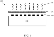
- FIG. 1 illustrates an example illumination device 100.
- Illumination device 100 includes a plurality of light sources 104 on a substrate 102, and a quantum dot (QD) film 106 disposed over light sources 104. Details of QD film 106 and the QDs within QD film 106 are provided later, and are not the focus of the embodiments described herein.
- Light sources 104 may be light emitting diodes (LEDs) that emit light at a lower wavelength (i.e., higher energy) than the emitted light from the quantum dots in QD film 106.
- LEDs light emitting diodes
- light sources 104 may emit light in the blue wavelength range (i.e., one or more wavelengths between about 440 nm and about 470 nm) while the QDs within QD film 106 include a first plurality of QDs that absorb the blue light and emit light in the green wavelength range (i.e., one or more wavelengths between about 520 nm and about 550 nm), and a second plurality of QDs that absorb the blue light and emit light in the red wavelength range (i.e., one or more wavelengths between about 620 nm and about 650 nm.)
- the emitted light 108 includes light in the blue wavelength range from light sources 104 that was not absorbed by QD film 106, and light in both the green and red wavelength ranges emitted from the QDs within QD film 106.
- the three primary colors are thus produced and may be filtered and combined downstream to produce any color.
- the filtering components are not shown for clarity, and are not critical with regards to the present embodiments.
- the illumination configuration of FIG. 1 suffers from optical losses due to unwanted scattering and absorption.
- the isotropic emission of the QDs within QD film 106 means that roughly half of the emitted light is directed back towards substrate 102 where it is either absorbed or scattered by substrate 102 and light sources 104. As a result, the overall efficiency of the illumination device is decreased due to the loss of usable emitted light.
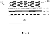
- FIG. 2 illustrates an illumination device 200.
- Illumination device 200 includes a beam splitting element 202 between QD film 106 and an array of light sources 204.
- Light sources 204 may be designed such that they only emit light in the blue wavelength range.
- Beam splitting element 202 may be a dichroic beam splitter that includes a plurality of stacked material layers chosen in such a way to allow certain wavelengths to pass through while reflecting other wavelengths.
- beam splitting element 202 is a removable element, such as a compound laminate structure, that includes the stacked material layers.
- beam splitting element 202 comprises a plurality of stacked thin films formed from extruded polymer layers, such as acrylic polymers. The total thickness of the stacked thin films may be less than 100 ⁇ m, thus allowing beam splitting element 202 to be highly flexible.
- Beam splitting element 202 may be designed such that it allows light in the blue wavelength range to pass through while reflecting light in the red and green wavelength ranges.
- the transmission spectra of beam splitting element 202 includes between 95% and 100% transmission of wavelengths less than about 490 nm, and less than 3% transmission of wavelengths greater than about 500 nm. For the wavelengths greater than about 500 nm, nearly all of the light is reflected. Given these optical properties, light in the blue wavelength range generated from light sources 204 will pass through beam splitting element 202 with low loss, while light in the red and green wavelength ranges emitted from the QDs within QD film 106 will be reflected back towards the front end of illumination device 200 (e.g., towards the user in the example where illumination device 200 is a display).
- emitted light 206 has a much greater light output compared to emitted light 108 from FIG. 1 .
- the overall efficiency of illumination device 200 may be increased by over 80% compared to illumination device 100 due to the presence of beam splitting element 202.
- FIG. 3 illustrates another illumination device 300, according to an embodiment.
- Illumination device 300 includes QD film 106 and light sources 204, with a thin film beam splitter 302 deposited over substrate 102 and light sources 204.
- Thin film beam splitter 302 may represent a plurality of stacked thin films designed to allow certain wavelengths to pass through while reflecting other wavelengths.
- Thin film beam splitter 302 may include similar optical properties to beam splitting element 202.
- a total thickness of thin film beam splitter 302 may be between about 1 ⁇ m and 50 ⁇ m.
- emitted light 304 has a much greater light output compared to emitted light 108 from FIG. 1 .
- Thin film beam splitter 302 may be deposited over substrate 102 and light sources 204 using a variety of methods.
- thin film beam splitter 302 is deposited using atomic layer deposition (ALD).
- ALD atomic layer deposition
- CVD chemical vapor deposition
- the CVD process may be plasmaenhanced (PECVD) or performed at a lower pressure than a typical CVD process (LPCVD).
- PECVD plasmaenhanced
- LPCVD typical CVD process
- thin film beam splitter 302 is deposited using sputtering. Any of the example techniques may be used to sequentially deposit each material layer to create a stack of layers that make up thin film beam splitter 302.
- a surface area of substrate 102 may be less than about 750 cm 2 , less than about 500 cm 2 , or less than about 100 cm 2 .
- substrate 102 is a flexible substrate made from a polymer material such as polyester (PET), polyimide (PI), polyethylene naphthalate (PEN), or polyetherimide (PEI) to name a few examples.
- light sources 204 include a plurality of microLEDs. MicroLEDs are different from typical LEDs or organic light emitting diodes (OLEDs). MicroLEDs are fabricated in an arrayed format with each individual microLED having a largest dimension in a range between about 1 ⁇ m and about 10 ⁇ m.
- MicroLEDs are also fabricated primarily from gallium nitride (GaN) or indium gallium nitride (InGaN). Due to their small size and design, microLEDs dissipate far less heat, and thus can be used effectively with either thin film beam splitter 302 or beam splitting element 202 without adversely affecting their optical properties.
- Example fabrication details for microLEDs may be found in U.S. Patent No. 9,019,595 .
- thin film beam splitter 302 has a fabrication process that can be integrated with the fabrication process of the microLEDs.
- the microLEDs and the thin film layers that make up thin film beam splitter 302 may be fabricated using similar process tools, making the overall fabrication less expensive and less complex.
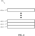
- FIG. 4 illustrates an example beam splitter 400, according to an embodiment.
- Beam splitter 400 may represent either thin film beam splitter 302 or beam splitting element 202.
- Beam splitter 400 includes a plurality of layers with the lowest layer identified as layer 402-1 and the upper-most layer identified as layer 402-n. The thickness and index of refraction of each of layers 402-1 through 402-n is chosen to provide the optical properties of beam splitter 400.
- beam splitter 400 includes alternating material layers of high and low refractive index.
- beam splitter 302 includes between 50 and 500 layers, with each layer having a thickness ranging between about 50 nm and about 100 nm.
- Example materials used for each layer 402-1 to 402-n include titanium dioxide (TiO 2 ), tantalum pentoxide (Ta 2 O 5 ), and silicon dioxide (SiO 2 ).
- the refractive index and thickness of each of layers 402-1 to 402-n is chosen to cause beam splitter 400 to transmit light having a wavelength less than about 490 (e.g., light in the blue wavelength range), while reflecting light having a wavelength greater than about 500 nm (e.g., light in the red and green wavelength ranges).
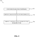
- FIG. 5 illustrates an example fabrication method 500 for an illumination device.
- Method 500 may be performed as part of a larger process for manufacturing an electronic device.
- Method 500 is not intended to be exhaustive and other steps may be performed without deviating from the scope of the invention.
- the various steps of method 500 may be performed in a different order than that illustrated.
- microLEDs are formed on a substrate.
- the substrate may be a semiconducting substrate.
- the substrate may be flexible.
- the microLEDs may be formed in an array with each microLED pixel having a largest dimension between about 1 ⁇ m and 10 ⁇ m.
- a beam splitter is disposed over the microLEDs.
- the beam splitter may be a separate element, such as a laminate compound or extruded polymer material containing multiple film layers, or the beam splitter may be a stack of sequentially deposited layers over the microLEDs.
- the layers may be deposited using a variety of techniques, such as ALD, CVD, and sputtering.
- a layer of quantum dots is disposed over the beam splitter.
- the layer of quantum dots may be provided in a quantum dot enhancement film (QDEF) as described in more detail later.
- QDEF quantum dot enhancement film
- the layer of quantum dots may be provided as a separate element, or it may be a deposited layer over the beam splitter.
- the QDs may be suspended in an amino silicone liquid and either spin-coated or cast over the beam splitter. Further materials that may be used to suspend the QDs are discussed in more detail later.
- FIG. 6 illustrates a cross-sectional structure of a barrier layer coated QD 600, according to an embodiment.
- Barrier layer coated QD 600 includes a QD 601 and a barrier layer 606.
- QD 601 includes a core 602 and a shell 604.
- Core 602 includes a semiconducting material that emits light upon absorption of higher energies.
- Examples of the semiconducting material for core 602 include indium phosphide (InP), cadmium selenide (CdSe), zinc sulfide (ZnS), lead sulfide (PbS), indium arsenide (InAs), indium gallium phosphide, (InGaP), cadmium zinc selenide (CdZnSe), zinc selenide (ZnSe) and cadmium telluride (CdTe). Any other II-VI, III-V, tertiary, or quaternary semiconductor structures that exhibit a direct band gap may be used as well.
- core 602 may also include one or more dopants such as, metals, alloys, to provide some examples.
- metal dopant may include, but not limited to, zinc (Zn), Copper (Cu), aluminum (Al), platinum (Pt), chrome (Cr), tungsten (W), palladium (Pd), or a combination thereof.
- the presence of one or more dopants in core 602 may improve structural and optical stability and quantum yield (QY) of QD 601 compared to undoped QDs.
- Core 602 may have a size of less than 20 nm in diameter, according to an embodiment. In another embodiment, core 602 may have a size between about 1 nm and about 5 nm in diameter.
- the ability to tailor the size of core 602, and consequently the size of QD 601 in the nanometer range enables photoemission coverage in the entire optical spectrum. In general, the larger QDs emit light towards the red end of the spectrum, while smaller QDs emit light towards the blue end of the spectrum. This effect arises as larger QDs have energy levels that are more closely spaced than the smaller QDs. This allows the QD to absorb photons containing less energy, i.e. those closer to the red end of the spectrum.
- Shell 604 surrounds core 602 and is disposed on outer surface of core 602.
- Shell 604 may include cadmium sulfide (CdS), zinc cadmium sulfide (ZnCdS), zinc selenide sulfide (ZnSeS), zinc selenide (ZnSe), and zinc sulfide (ZnS).
- shell 604 may have a thickness of, for example, one or more monolayers. In other embodiments, shell 604 may have a thickness between about 1 nm and about 5 nm. Shell 604 may be utilized to help reduce the lattice mismatch with core 602 and improve the QY of QD 601.
- Shell 604 may also help to passivate and remove surface trap states, such as dangling bonds, on core 602 to increase QY of QD 601.
- surface trap states such as dangling bonds
- the presence of surface trap states may provide non-radiative recombination centers and contribute to lowered emission efficiency of QD 601.
- QD 601 may include a second shell disposed on shell 604, or more than two shells surrounding core 602, without departing from the scope of the present invention.
- the second shell may be on the order of two monolayers thick and is typically, though not required, also a semiconducting material.
- Second shell may provide protection to core 602.
- Second shell material may be zinc sulfide (ZnS) or zinc selenide (ZnSe), although other materials may be used as well without deviating from the scope of the invention.
- Barrier layer 606 is configured to form a coating on QD 601.
- barrier layer 606 is disposed on and in substantial contact with outer an outer surface of shell 604.
- barrier layer 606 may be disposed on the outermost shell of QD 601.
- barrier layer 606 is configured to act as a spacer between QD 601 and one or more QDs in, for example, a solution, a composition, and/or a film having a plurality of QDs, where the plurality of QDs may be similar to QD 601 and/or barrier layer coated QD 600.
- barrier layer 606 may help to prevent aggregation of QD 601 with adjacent QDs. Aggregation of QD 601 with adjacent QDs may lead to increase in size of QD 601 and consequent reduction or quenching in the optical emission properties of the aggregated QD (not shown) including QD 601. As discussed above, optical characteristics of QDs are size dependent, and thus increase in QD size due to aggregation leads to the quenching phenomenon. Barrier layer 606 may also prevent QD 601 from reabsorbing optical emissions from other QDs in the QD solutions, QD compositions, and/or QD films and thus, improve the QY of these QD solutions, QD compositions, and/or QD films.
- barrier layer 606 provides protection to QD 601 from, for example, moisture, air, and/or harsh environments (e.g., high temperatures and chemicals used during lithographic processing of QDs and/or during manufacturing process of QD based devices) that may adversely affect the structural and optical properties of QD 601.
- moisture, air, and/or harsh environments e.g., high temperatures and chemicals used during lithographic processing of QDs and/or during manufacturing process of QD based devices
- Barrier layer 606 includes one or more materials that are amorphous, optically transparent and/or electrically inactive. Suitable barrier layers include inorganic materials, such as, but not limited to, inorganic oxides and/or nitrides. Examples of materials for barrier layer 606 include oxides and/or nitrides of Al, Ba, Ca, Mg, Ni, Si, Ti, or Zr, according to various embodiments. Barrier layer 606 may have a thickness ranging from about 8 nm to about 15 nm in various embodiments.
- the thickness of barrier layer 606 may have a minimum value such that a center-to-center distance between two adjacent QDs 600, for example, in a solution, composition, and/or film is equal to or greater than a Forster radius (also referred in the art as Forster distance) in order to reduce or substantially eliminate resonance energy transfer and/or reabsorption of optical emission between the adjacent QDs 600, and consequently, improve QY of the adjacent QDs 600.
- the thickness of barrier layer 606 may have a minimum value of between about 8 nm to about 15nm.
- Forster radius may refer to a center-to-center distance between two adjacent QDs, such as QDs 600 at which resonance energy transfer efficiency between these two adjacent QDs is about 50%. Having a center-to-center distance between two adjacent QDs greater than the Forster radius may decrease the resonance energy transfer efficiency and improve the optical emission properties and QY of the adjacent QDs.
- the process of resonance energy transfer can take place when one QD in an electronically excited state transfers its excitation energy to a nearby or adjacent QD.
- the resonance energy transfer process is a non-radiative quantum mechanical process. Thus, when the resonance energy transfer occurs from the one QD, the optical emission properties of the one QD may be quenched and the QY of the one QD may be adversely affected.
- barrier layer coated QD 600 may additionally or optionally include a plurality of ligands or surfactants 608, according to an embodiment.
- Ligands or surfactants 608 may be adsorbed or bound to an outer surface of barrier layer coated QD 600, such as on an outer surface of barrier layer 606, according to an embodiment.
- the plurality of ligands or surfactants 608 may include hydrophilic or polar heads 608a and hydrophobic or non-polar tails 608b. The hydrophilic or polar heads 608a may be bound to barrier layer 606.
- ligands or surfactants 608 may help to separate QD 600 and/or QD 601 from other QDs in, for example, a solution, a composition, and/or a film during their formation. If the QDs are allowed to aggregate during their formation, the quantum efficiency of QDs such as QD 600 and/or QD 601 may drop and quench the optical emission properties of these QDs.
- Ligands or surfactants 608 may also be used to impart certain properties to barrier layer coated QD 600, such as hydrophobicity to provide miscibility in non-polar solvents, or to provide reaction sites (e.g., reverse micellar systems) for other compounds to bind.
- the ligand is a fatty acid selected from lauric acid, caproic acid, myristic acid, palmitic acid, stearic acid, and oleic acid.
- the ligand is an organic phosphine or an organic phosphine oxide selected from trioctylphosphine oxide (TOPO), trioctylphosphine (TOP), diphenylphosphine (DPP), triphenylphosphine oxide, and tributylphosphine oxide.
- TOPO trioctylphosphine oxide
- TOP trioctylphosphine
- DPP diphenylphosphine
- triphenylphosphine oxide and tributylphosphine oxide.
- the ligand is an amine selected from dodecylamine, oleylamine, hexadecylamine, and octadecylamine. In some embodiments, the ligand is trioctylphosphine (TOP). In some embodiments, the ligand is oleylamine. In some embodiments, the ligand is diphenylphosphine.
- Nonionic surfactants may be used as surfactants 608.
- Some examples of nonionic surfactants include polyoxyethylene nonylphenylether (commercial name IGEPAL CO-520), IGEPAL CO-630, IGEPAL CA-630, and Arkopal N 100.
- QDs 601 and/or 600 may be synthesized to emit light in the red, orange, and/or yellow range. In some embodiments, QDs 601 and/or 600 may be synthesized emit light in the green and/or yellow range. In some embodiments, QDs 601 and/or 600 may be synthesized emit light in the blue, indigo, violet, and/or ultra-violet range. In some embodiments, QDs 601 and/or 600 may be synthesized to have a primary emission peak wavelength between about 605 nm and about 650 nm, between about 510 nm and about 550 nm, or between about 300 nm and about 480 nm.
- QDs 601 and/or 600 may be synthesized to display a high QY. In some embodiments, QDs 601 and/or 600 may be synthesized to display a QY between 80% and 95% or between 85% and 90%.
- QDs 600 may be synthesized such that the presence of barrier layer 606 on QDs 601 does not substantially change or quench the optical emission properties of QDs 601.
- the subscripts ST and X denote the standard (reference dye) and the core/shell QDs solution (test sample), respectively.
- ⁇ X is the quantum yield of the core/shell QDs
- ⁇ ST is the quantum yield of the reference dye.
- Grad (I/A), where I is the area under the emission peak (wavelength scale); A is the absorbance at excitation wavelength.
- ⁇ is the refractive index of the reference dye or the core/shell QDs in the solvent. See, e.g., Williams et al. (1983) "Relative fluorescence quantum yields using a computer controlled luminescence spectrometer" Analyst 108:1067 .
- the references listed in Williams et al. are for green and red emitting QDs.
- FIG. 7 illustrates an example of a quantum dot enhancement film (QDEF) 700.
- QDEF 700 is one example of QD film 106.
- Quantum dot enhancement film 700 includes a bottom layer 704, a top layer 706, and a quantum dot layer 702 sandwiched between.
- Bottom layer 704 and top layer 706 may be a variety of materials that are substantially transparent to visible wavelengths (e.g., 400 - 700 nm.)
- bottom layer 704 and top layer 706 may be glass or polyethylene terephthalate (PET).
- PET polyethylene terephthalate
- Bottom layer 704 and top layer 706 may also by polyester coated with aluminum oxide.
- Other polymers may be used as well that exhibit low oxygen permeability and low absorption for the wavelengths being emitted by the quantum dots trapped within quantum dot layer 702. It is not necessary that bottom layer 704 and top layer 706 be comprised of the same material.
- Quantum dot layer 702 includes a plurality of quantum dots within an adhesive material. According to an embodiment, quantum dot layer 702 has a thickness between about 50 and 150 micrometers ( ⁇ m) and is used as a light down conversion layer. Quantum dot layer 702 may have a thickness around 100 ⁇ m. The adhesive material binds to both bottom layer 704 and top layer 706, holding the sandwich-like structure together.
- the plurality of quantum dots includes sizes that emit in at least one of the green and red visible wavelength spectrums.
- the quantum dots are protected in quantum dot layer 702 from environmental effects and kept separated from one another to avoid quenching.
- the quantum dots may be spatially separated by enough distance such that quenching processes like excited state reactions, energy transfer, complex-formation and collisional quenching do not occur.
- quantum dots are mixed within an amino silicone liquid and are emulsified into an epoxy resin that is coated to form quantum dot layer 702.
- Other example materials for use in quantum dot layer 702 include acrylates, epoxies, acrylated epoxies, ethylene-vinyl acetate, thiol-enes, polyurethane, polyethers, polyols, and polyesters. Further details regarding the fabrication and operation of quantum dot enhancement films may be found in U. S. Patent No. 9,199,842 .
Landscapes
- Engineering & Computer Science (AREA)
- Chemical & Material Sciences (AREA)
- Power Engineering (AREA)
- Microelectronics & Electronic Packaging (AREA)
- Physics & Mathematics (AREA)
- Materials Engineering (AREA)
- Organic Chemistry (AREA)
- Computer Hardware Design (AREA)
- General Physics & Mathematics (AREA)
- Condensed Matter Physics & Semiconductors (AREA)
- Inorganic Chemistry (AREA)
- Spectroscopy & Molecular Physics (AREA)
- General Engineering & Computer Science (AREA)
- Optical Filters (AREA)
- Led Device Packages (AREA)
- Non-Portable Lighting Devices Or Systems Thereof (AREA)
- Planar Illumination Modules (AREA)
- Luminescent Compositions (AREA)
Applications Claiming Priority (3)
| Application Number | Priority Date | Filing Date | Title |
|---|---|---|---|
| US201762477716P | 2017-03-28 | 2017-03-28 | |
| US15/935,507 US10546985B2 (en) | 2017-03-28 | 2018-03-26 | Method for increasing the light output of microLED devices using quantum dots |
| PCT/US2018/024540 WO2018183308A1 (en) | 2017-03-28 | 2018-03-27 | Method for increasing the light output of microled devices using quantum dots |
Publications (2)
| Publication Number | Publication Date |
|---|---|
| EP3601480A1 EP3601480A1 (en) | 2020-02-05 |
| EP3601480B1 true EP3601480B1 (en) | 2022-12-21 |
Family
ID=63669936
Family Applications (1)
| Application Number | Title | Priority Date | Filing Date |
|---|---|---|---|
| EP18718049.2A Active EP3601480B1 (en) | 2017-03-28 | 2018-03-27 | Method for increasing the light output of microled devices using quantum dots |
Country Status (8)
| Country | Link |
|---|---|
| US (3) | US10546985B2 (enExample) |
| EP (1) | EP3601480B1 (enExample) |
| JP (1) | JP7191033B2 (enExample) |
| KR (1) | KR20190131530A (enExample) |
| CN (1) | CN110582551A (enExample) |
| AU (1) | AU2018244291B2 (enExample) |
| CA (1) | CA3057983A1 (enExample) |
| WO (1) | WO2018183308A1 (enExample) |
Families Citing this family (4)
| Publication number | Priority date | Publication date | Assignee | Title |
|---|---|---|---|---|
| CN109920344A (zh) * | 2019-03-22 | 2019-06-21 | 深圳康佳电子科技有限公司 | 一种无缝拼接的Micro LED显示装置 |
| CN111010232B (zh) * | 2019-12-20 | 2021-03-12 | 厦门大学 | 一种提高可见光通信中Micro-LED带宽方法 |
| US11575065B2 (en) | 2021-01-29 | 2023-02-07 | Applied Materials, Inc. | Tuning of emission properties of quantum emission devices using strain-tuned piezoelectric template layers |
| JP7643987B2 (ja) | 2021-11-18 | 2025-03-11 | 信越化学工業株式会社 | 量子ドットのパターニング方法、光学素子の製造方法、バックライトユニットの製造方法及び画像表示装置の製造方法 |
Family Cites Families (22)
| Publication number | Priority date | Publication date | Assignee | Title |
|---|---|---|---|---|
| US7367691B2 (en) * | 2003-06-16 | 2008-05-06 | Industrial Technology Research Institute | Omnidirectional one-dimensional photonic crystal and light emitting device made from the same |
| US20070262714A1 (en) * | 2006-05-15 | 2007-11-15 | X-Rite, Incorporated | Illumination source including photoluminescent material and a filter, and an apparatus including same |
| JP2009105379A (ja) | 2007-10-05 | 2009-05-14 | Panasonic Electric Works Co Ltd | 発光装置 |
| JP4613947B2 (ja) | 2007-12-07 | 2011-01-19 | ソニー株式会社 | 照明装置、色変換素子及び表示装置 |
| US8169135B2 (en) | 2008-12-17 | 2012-05-01 | Lednovation, Inc. | Semiconductor lighting device with wavelength conversion on back-transferred light path |
| US8434914B2 (en) * | 2009-12-11 | 2013-05-07 | Osram Sylvania Inc. | Lens generating a batwing-shaped beam distribution, and method therefor |
| CN101937959A (zh) * | 2010-08-12 | 2011-01-05 | 武汉华灿光电有限公司 | 带滤光膜的发光二极管及其制造方法 |
| KR102098682B1 (ko) | 2010-11-10 | 2020-05-22 | 나노시스, 인크. | 양자 도트 필름들, 조명 디바이스들, 및 조명 방법들 |
| KR20140046419A (ko) | 2011-05-16 | 2014-04-18 | 베르라세 테크놀러지스 엘엘씨 | 공진기가 향상된 광전자 장치 및 그 제조 방법 |
| WO2013112435A1 (en) * | 2012-01-24 | 2013-08-01 | Cooledge Lighting Inc. | Light - emitting devices having discrete phosphor chips and fabrication methods |
| CN103576370A (zh) * | 2012-07-23 | 2014-02-12 | 天津富纳源创科技有限公司 | 偏光片 |
| JP6680670B2 (ja) * | 2013-04-11 | 2020-04-15 | ルミレッズ ホールディング ベーフェー | トップエミッション型半導体発光デバイス |
| US9484504B2 (en) * | 2013-05-14 | 2016-11-01 | Apple Inc. | Micro LED with wavelength conversion layer |
| US8928021B1 (en) | 2013-06-18 | 2015-01-06 | LuxVue Technology Corporation | LED light pipe |
| CN105829103B (zh) * | 2013-12-20 | 2018-10-19 | 3M创新有限公司 | 边缘侵入得到改善的量子点制品 |
| JP6519311B2 (ja) * | 2014-06-27 | 2019-05-29 | 日亜化学工業株式会社 | 発光装置 |
| KR20160025456A (ko) * | 2014-08-27 | 2016-03-08 | 서울바이오시스 주식회사 | 발광 다이오드 및 그 제조 방법 |
| CN104617197B (zh) * | 2015-01-08 | 2017-08-01 | 青岛海信电器股份有限公司 | 一种显示模组用led发光器件及显示模组 |
| KR102538377B1 (ko) | 2015-05-20 | 2023-06-01 | 도레이 카부시키가이샤 | 조명 장치 및 표시 장치 |
| US9841548B2 (en) | 2015-06-30 | 2017-12-12 | Apple Inc. | Electronic devices with soft input-output components |
| US10297581B2 (en) * | 2015-07-07 | 2019-05-21 | Apple Inc. | Quantum dot integration schemes |
| CN105096749B (zh) * | 2015-08-04 | 2017-07-04 | 京东方科技集团股份有限公司 | 一种显示装置及其制备方法 |
-
2018
- 2018-03-26 US US15/935,507 patent/US10546985B2/en active Active
- 2018-03-27 WO PCT/US2018/024540 patent/WO2018183308A1/en not_active Ceased
- 2018-03-27 KR KR1020197031026A patent/KR20190131530A/ko not_active Abandoned
- 2018-03-27 CA CA3057983A patent/CA3057983A1/en active Pending
- 2018-03-27 EP EP18718049.2A patent/EP3601480B1/en active Active
- 2018-03-27 JP JP2019551987A patent/JP7191033B2/ja active Active
- 2018-03-27 CN CN201880029719.4A patent/CN110582551A/zh active Pending
- 2018-03-27 AU AU2018244291A patent/AU2018244291B2/en active Active
-
2020
- 2020-01-27 US US16/773,543 patent/US11201270B2/en active Active
-
2021
- 2021-12-13 US US17/549,543 patent/US20220278258A1/en not_active Abandoned
Also Published As
| Publication number | Publication date |
|---|---|
| US11201270B2 (en) | 2021-12-14 |
| AU2018244291B2 (en) | 2024-02-01 |
| CA3057983A1 (en) | 2018-10-04 |
| EP3601480A1 (en) | 2020-02-05 |
| WO2018183308A1 (en) | 2018-10-04 |
| CN110582551A (zh) | 2019-12-17 |
| US10546985B2 (en) | 2020-01-28 |
| JP2020516015A (ja) | 2020-05-28 |
| JP7191033B2 (ja) | 2022-12-16 |
| US20200161517A1 (en) | 2020-05-21 |
| US20220278258A1 (en) | 2022-09-01 |
| KR20190131530A (ko) | 2019-11-26 |
| US20180287025A1 (en) | 2018-10-04 |
| AU2018244291A1 (en) | 2019-10-24 |
Similar Documents
| Publication | Publication Date | Title |
|---|---|---|
| US11824146B2 (en) | Quantum dot encapsulation techniques | |
| US20220278258A1 (en) | Method for increasing the light output of microled devicecs using quantum dots | |
| AU2017350734B2 (en) | Backlight unit for a display device | |
| US11092850B2 (en) | Using multiple excitation wavelengths in nanostructure based display devices | |
| US11428988B2 (en) | Increasing color gamut performance and efficiency in quantum dot color conversion layers | |
| CN110780486A (zh) | 使用具有集成光学元件的量子点改善显示效率的方法 | |
| EP3658983B1 (en) | Nanostructure based display devices | |
| US20220206341A1 (en) | Nanostructure based display devices with improved light extraction efficiency | |
| US11886073B2 (en) | Nanostructure based display devices |
Legal Events
| Date | Code | Title | Description |
|---|---|---|---|
| STAA | Information on the status of an ep patent application or granted ep patent |
Free format text: STATUS: UNKNOWN |
|
| STAA | Information on the status of an ep patent application or granted ep patent |
Free format text: STATUS: THE INTERNATIONAL PUBLICATION HAS BEEN MADE |
|
| PUAI | Public reference made under article 153(3) epc to a published international application that has entered the european phase |
Free format text: ORIGINAL CODE: 0009012 |
|
| STAA | Information on the status of an ep patent application or granted ep patent |
Free format text: STATUS: REQUEST FOR EXAMINATION WAS MADE |
|
| 17P | Request for examination filed |
Effective date: 20190925 |
|
| AK | Designated contracting states |
Kind code of ref document: A1 Designated state(s): AL AT BE BG CH CY CZ DE DK EE ES FI FR GB GR HR HU IE IS IT LI LT LU LV MC MK MT NL NO PL PT RO RS SE SI SK SM TR |
|
| AX | Request for extension of the european patent |
Extension state: BA ME |
|
| DAV | Request for validation of the european patent (deleted) | ||
| DAX | Request for extension of the european patent (deleted) | ||
| STAA | Information on the status of an ep patent application or granted ep patent |
Free format text: STATUS: EXAMINATION IS IN PROGRESS |
|
| 17Q | First examination report despatched |
Effective date: 20220218 |
|
| GRAP | Despatch of communication of intention to grant a patent |
Free format text: ORIGINAL CODE: EPIDOSNIGR1 |
|
| STAA | Information on the status of an ep patent application or granted ep patent |
Free format text: STATUS: GRANT OF PATENT IS INTENDED |
|
| INTG | Intention to grant announced |
Effective date: 20220714 |
|
| GRAS | Grant fee paid |
Free format text: ORIGINAL CODE: EPIDOSNIGR3 |
|
| GRAA | (expected) grant |
Free format text: ORIGINAL CODE: 0009210 |
|
| STAA | Information on the status of an ep patent application or granted ep patent |
Free format text: STATUS: THE PATENT HAS BEEN GRANTED |
|
| AK | Designated contracting states |
Kind code of ref document: B1 Designated state(s): AL AT BE BG CH CY CZ DE DK EE ES FI FR GB GR HR HU IE IS IT LI LT LU LV MC MK MT NL NO PL PT RO RS SE SI SK SM TR |
|
| REG | Reference to a national code |
Ref country code: GB Ref legal event code: FG4D |
|
| REG | Reference to a national code |
Ref country code: CH Ref legal event code: EP |
|
| REG | Reference to a national code |
Ref country code: DE Ref legal event code: R096 Ref document number: 602018044475 Country of ref document: DE |
|
| REG | Reference to a national code |
Ref country code: AT Ref legal event code: REF Ref document number: 1539069 Country of ref document: AT Kind code of ref document: T Effective date: 20230115 |
|
| REG | Reference to a national code |
Ref country code: IE Ref legal event code: FG4D |
|
| REG | Reference to a national code |
Ref country code: NL Ref legal event code: FP |
|
| REG | Reference to a national code |
Ref country code: LT Ref legal event code: MG9D |
|
| PG25 | Lapsed in a contracting state [announced via postgrant information from national office to epo] |
Ref country code: SE Free format text: LAPSE BECAUSE OF FAILURE TO SUBMIT A TRANSLATION OF THE DESCRIPTION OR TO PAY THE FEE WITHIN THE PRESCRIBED TIME-LIMIT Effective date: 20221221 Ref country code: NO Free format text: LAPSE BECAUSE OF FAILURE TO SUBMIT A TRANSLATION OF THE DESCRIPTION OR TO PAY THE FEE WITHIN THE PRESCRIBED TIME-LIMIT Effective date: 20230321 Ref country code: LT Free format text: LAPSE BECAUSE OF FAILURE TO SUBMIT A TRANSLATION OF THE DESCRIPTION OR TO PAY THE FEE WITHIN THE PRESCRIBED TIME-LIMIT Effective date: 20221221 Ref country code: FI Free format text: LAPSE BECAUSE OF FAILURE TO SUBMIT A TRANSLATION OF THE DESCRIPTION OR TO PAY THE FEE WITHIN THE PRESCRIBED TIME-LIMIT Effective date: 20221221 |
|
| REG | Reference to a national code |
Ref country code: AT Ref legal event code: MK05 Ref document number: 1539069 Country of ref document: AT Kind code of ref document: T Effective date: 20221221 |
|
| PG25 | Lapsed in a contracting state [announced via postgrant information from national office to epo] |
Ref country code: RS Free format text: LAPSE BECAUSE OF FAILURE TO SUBMIT A TRANSLATION OF THE DESCRIPTION OR TO PAY THE FEE WITHIN THE PRESCRIBED TIME-LIMIT Effective date: 20221221 Ref country code: LV Free format text: LAPSE BECAUSE OF FAILURE TO SUBMIT A TRANSLATION OF THE DESCRIPTION OR TO PAY THE FEE WITHIN THE PRESCRIBED TIME-LIMIT Effective date: 20221221 Ref country code: HR Free format text: LAPSE BECAUSE OF FAILURE TO SUBMIT A TRANSLATION OF THE DESCRIPTION OR TO PAY THE FEE WITHIN THE PRESCRIBED TIME-LIMIT Effective date: 20221221 Ref country code: GR Free format text: LAPSE BECAUSE OF FAILURE TO SUBMIT A TRANSLATION OF THE DESCRIPTION OR TO PAY THE FEE WITHIN THE PRESCRIBED TIME-LIMIT Effective date: 20230322 |
|
| P01 | Opt-out of the competence of the unified patent court (upc) registered |
Effective date: 20230523 |
|
| PG25 | Lapsed in a contracting state [announced via postgrant information from national office to epo] |
Ref country code: SM Free format text: LAPSE BECAUSE OF FAILURE TO SUBMIT A TRANSLATION OF THE DESCRIPTION OR TO PAY THE FEE WITHIN THE PRESCRIBED TIME-LIMIT Effective date: 20221221 Ref country code: RO Free format text: LAPSE BECAUSE OF FAILURE TO SUBMIT A TRANSLATION OF THE DESCRIPTION OR TO PAY THE FEE WITHIN THE PRESCRIBED TIME-LIMIT Effective date: 20221221 Ref country code: PT Free format text: LAPSE BECAUSE OF FAILURE TO SUBMIT A TRANSLATION OF THE DESCRIPTION OR TO PAY THE FEE WITHIN THE PRESCRIBED TIME-LIMIT Effective date: 20230421 Ref country code: ES Free format text: LAPSE BECAUSE OF FAILURE TO SUBMIT A TRANSLATION OF THE DESCRIPTION OR TO PAY THE FEE WITHIN THE PRESCRIBED TIME-LIMIT Effective date: 20221221 Ref country code: EE Free format text: LAPSE BECAUSE OF FAILURE TO SUBMIT A TRANSLATION OF THE DESCRIPTION OR TO PAY THE FEE WITHIN THE PRESCRIBED TIME-LIMIT Effective date: 20221221 Ref country code: CZ Free format text: LAPSE BECAUSE OF FAILURE TO SUBMIT A TRANSLATION OF THE DESCRIPTION OR TO PAY THE FEE WITHIN THE PRESCRIBED TIME-LIMIT Effective date: 20221221 Ref country code: AT Free format text: LAPSE BECAUSE OF FAILURE TO SUBMIT A TRANSLATION OF THE DESCRIPTION OR TO PAY THE FEE WITHIN THE PRESCRIBED TIME-LIMIT Effective date: 20221221 |
|
| PG25 | Lapsed in a contracting state [announced via postgrant information from national office to epo] |
Ref country code: SK Free format text: LAPSE BECAUSE OF FAILURE TO SUBMIT A TRANSLATION OF THE DESCRIPTION OR TO PAY THE FEE WITHIN THE PRESCRIBED TIME-LIMIT Effective date: 20221221 Ref country code: PL Free format text: LAPSE BECAUSE OF FAILURE TO SUBMIT A TRANSLATION OF THE DESCRIPTION OR TO PAY THE FEE WITHIN THE PRESCRIBED TIME-LIMIT Effective date: 20221221 Ref country code: IS Free format text: LAPSE BECAUSE OF FAILURE TO SUBMIT A TRANSLATION OF THE DESCRIPTION OR TO PAY THE FEE WITHIN THE PRESCRIBED TIME-LIMIT Effective date: 20230421 Ref country code: AL Free format text: LAPSE BECAUSE OF FAILURE TO SUBMIT A TRANSLATION OF THE DESCRIPTION OR TO PAY THE FEE WITHIN THE PRESCRIBED TIME-LIMIT Effective date: 20221221 |
|
| REG | Reference to a national code |
Ref country code: DE Ref legal event code: R097 Ref document number: 602018044475 Country of ref document: DE |
|
| PLBE | No opposition filed within time limit |
Free format text: ORIGINAL CODE: 0009261 |
|
| STAA | Information on the status of an ep patent application or granted ep patent |
Free format text: STATUS: NO OPPOSITION FILED WITHIN TIME LIMIT |
|
| PG25 | Lapsed in a contracting state [announced via postgrant information from national office to epo] |
Ref country code: MC Free format text: LAPSE BECAUSE OF FAILURE TO SUBMIT A TRANSLATION OF THE DESCRIPTION OR TO PAY THE FEE WITHIN THE PRESCRIBED TIME-LIMIT Effective date: 20221221 Ref country code: DK Free format text: LAPSE BECAUSE OF FAILURE TO SUBMIT A TRANSLATION OF THE DESCRIPTION OR TO PAY THE FEE WITHIN THE PRESCRIBED TIME-LIMIT Effective date: 20221221 |
|
| REG | Reference to a national code |
Ref country code: CH Ref legal event code: PL |
|
| REG | Reference to a national code |
Ref country code: NL Ref legal event code: PD Owner name: SHOEI CHEMICAL INC.; JP Free format text: DETAILS ASSIGNMENT: CHANGE OF OWNER(S), ASSIGNMENT; FORMER OWNER NAME: NANOSYS, INC. Effective date: 20231023 |
|
| REG | Reference to a national code |
Ref country code: DE Ref legal event code: R081 Ref document number: 602018044475 Country of ref document: DE Owner name: SHOEI CHEMICAL INC., JP Free format text: FORMER OWNER: NANOSYS, INC., MILPITAS, CA, US |
|
| 26N | No opposition filed |
Effective date: 20230922 |
|
| REG | Reference to a national code |
Ref country code: GB Ref legal event code: 732E Free format text: REGISTERED BETWEEN 20231102 AND 20231108 |
|
| REG | Reference to a national code |
Ref country code: BE Ref legal event code: MM Effective date: 20230331 |
|
| PG25 | Lapsed in a contracting state [announced via postgrant information from national office to epo] |
Ref country code: LU Free format text: LAPSE BECAUSE OF NON-PAYMENT OF DUE FEES Effective date: 20230327 |
|
| REG | Reference to a national code |
Ref country code: IE Ref legal event code: MM4A |
|
| PG25 | Lapsed in a contracting state [announced via postgrant information from national office to epo] |
Ref country code: SI Free format text: LAPSE BECAUSE OF FAILURE TO SUBMIT A TRANSLATION OF THE DESCRIPTION OR TO PAY THE FEE WITHIN THE PRESCRIBED TIME-LIMIT Effective date: 20221221 Ref country code: LI Free format text: LAPSE BECAUSE OF NON-PAYMENT OF DUE FEES Effective date: 20230331 Ref country code: IE Free format text: LAPSE BECAUSE OF NON-PAYMENT OF DUE FEES Effective date: 20230327 Ref country code: CH Free format text: LAPSE BECAUSE OF NON-PAYMENT OF DUE FEES Effective date: 20230331 |
|
| PG25 | Lapsed in a contracting state [announced via postgrant information from national office to epo] |
Ref country code: BE Free format text: LAPSE BECAUSE OF NON-PAYMENT OF DUE FEES Effective date: 20230331 |
|
| PG25 | Lapsed in a contracting state [announced via postgrant information from national office to epo] |
Ref country code: IT Free format text: LAPSE BECAUSE OF FAILURE TO SUBMIT A TRANSLATION OF THE DESCRIPTION OR TO PAY THE FEE WITHIN THE PRESCRIBED TIME-LIMIT Effective date: 20221221 |
|
| PG25 | Lapsed in a contracting state [announced via postgrant information from national office to epo] |
Ref country code: BG Free format text: LAPSE BECAUSE OF FAILURE TO SUBMIT A TRANSLATION OF THE DESCRIPTION OR TO PAY THE FEE WITHIN THE PRESCRIBED TIME-LIMIT Effective date: 20221221 |
|
| PG25 | Lapsed in a contracting state [announced via postgrant information from national office to epo] |
Ref country code: BG Free format text: LAPSE BECAUSE OF FAILURE TO SUBMIT A TRANSLATION OF THE DESCRIPTION OR TO PAY THE FEE WITHIN THE PRESCRIBED TIME-LIMIT Effective date: 20221221 |
|
| PGFP | Annual fee paid to national office [announced via postgrant information from national office to epo] |
Ref country code: DE Payment date: 20250319 Year of fee payment: 8 |
|
| PGFP | Annual fee paid to national office [announced via postgrant information from national office to epo] |
Ref country code: NL Payment date: 20250319 Year of fee payment: 8 |
|
| PGFP | Annual fee paid to national office [announced via postgrant information from national office to epo] |
Ref country code: FR Payment date: 20250326 Year of fee payment: 8 |
|
| PGFP | Annual fee paid to national office [announced via postgrant information from national office to epo] |
Ref country code: GB Payment date: 20250324 Year of fee payment: 8 |
|
| PG25 | Lapsed in a contracting state [announced via postgrant information from national office to epo] |
Ref country code: CY Free format text: LAPSE BECAUSE OF FAILURE TO SUBMIT A TRANSLATION OF THE DESCRIPTION OR TO PAY THE FEE WITHIN THE PRESCRIBED TIME-LIMIT; INVALID AB INITIO Effective date: 20180327 |
|
| PG25 | Lapsed in a contracting state [announced via postgrant information from national office to epo] |
Ref country code: HU Free format text: LAPSE BECAUSE OF FAILURE TO SUBMIT A TRANSLATION OF THE DESCRIPTION OR TO PAY THE FEE WITHIN THE PRESCRIBED TIME-LIMIT; INVALID AB INITIO Effective date: 20180327 |