EP3599806A1 - Verfahren zum montieren eines elektrischen bauteils auf einem sockelteil - Google Patents
Verfahren zum montieren eines elektrischen bauteils auf einem sockelteil Download PDFInfo
- Publication number
- EP3599806A1 EP3599806A1 EP19183152.8A EP19183152A EP3599806A1 EP 3599806 A1 EP3599806 A1 EP 3599806A1 EP 19183152 A EP19183152 A EP 19183152A EP 3599806 A1 EP3599806 A1 EP 3599806A1
- Authority
- EP
- European Patent Office
- Prior art keywords
- base part
- electrical component
- wedge
- wedge element
- template
- Prior art date
- Legal status (The legal status is an assumption and is not a legal conclusion. Google has not performed a legal analysis and makes no representation as to the accuracy of the status listed.)
- Granted
Links
Images


Classifications
-
- H—ELECTRICITY
- H05—ELECTRIC TECHNIQUES NOT OTHERWISE PROVIDED FOR
- H05K—PRINTED CIRCUITS; CASINGS OR CONSTRUCTIONAL DETAILS OF ELECTRIC APPARATUS; MANUFACTURE OF ASSEMBLAGES OF ELECTRICAL COMPONENTS
- H05K7/00—Constructional details common to different types of electric apparatus
- H05K7/20—Modifications to facilitate cooling, ventilating, or heating
- H05K7/2039—Modifications to facilitate cooling, ventilating, or heating characterised by the heat transfer by conduction from the heat generating element to a dissipating body
- H05K7/20436—Inner thermal coupling elements in heat dissipating housings, e.g. protrusions or depressions integrally formed in the housing
- H05K7/2049—Pressing means used to urge contact, e.g. springs
-
- H—ELECTRICITY
- H10—SEMICONDUCTOR DEVICES; ELECTRIC SOLID-STATE DEVICES NOT OTHERWISE PROVIDED FOR
- H10F—INORGANIC SEMICONDUCTOR DEVICES SENSITIVE TO INFRARED RADIATION, LIGHT, ELECTROMAGNETIC RADIATION OF SHORTER WAVELENGTH OR CORPUSCULAR RADIATION
- H10F77/00—Constructional details of devices covered by this subclass
- H10F77/60—Arrangements for cooling, heating, ventilating or compensating for temperature fluctuations
-
- H—ELECTRICITY
- H05—ELECTRIC TECHNIQUES NOT OTHERWISE PROVIDED FOR
- H05K—PRINTED CIRCUITS; CASINGS OR CONSTRUCTIONAL DETAILS OF ELECTRIC APPARATUS; MANUFACTURE OF ASSEMBLAGES OF ELECTRICAL COMPONENTS
- H05K7/00—Constructional details common to different types of electric apparatus
- H05K7/20—Modifications to facilitate cooling, ventilating, or heating
- H05K7/2039—Modifications to facilitate cooling, ventilating, or heating characterised by the heat transfer by conduction from the heat generating element to a dissipating body
- H05K7/20436—Inner thermal coupling elements in heat dissipating housings, e.g. protrusions or depressions integrally formed in the housing
- H05K7/20445—Inner thermal coupling elements in heat dissipating housings, e.g. protrusions or depressions integrally formed in the housing the coupling element being an additional piece, e.g. thermal standoff
-
- H—ELECTRICITY
- H10—SEMICONDUCTOR DEVICES; ELECTRIC SOLID-STATE DEVICES NOT OTHERWISE PROVIDED FOR
- H10F—INORGANIC SEMICONDUCTOR DEVICES SENSITIVE TO INFRARED RADIATION, LIGHT, ELECTROMAGNETIC RADIATION OF SHORTER WAVELENGTH OR CORPUSCULAR RADIATION
- H10F71/00—Manufacture or treatment of devices covered by this subclass
-
- H—ELECTRICITY
- H10—SEMICONDUCTOR DEVICES; ELECTRIC SOLID-STATE DEVICES NOT OTHERWISE PROVIDED FOR
- H10F—INORGANIC SEMICONDUCTOR DEVICES SENSITIVE TO INFRARED RADIATION, LIGHT, ELECTROMAGNETIC RADIATION OF SHORTER WAVELENGTH OR CORPUSCULAR RADIATION
- H10F77/00—Constructional details of devices covered by this subclass
- H10F77/50—Encapsulations or containers
-
- H—ELECTRICITY
- H10—SEMICONDUCTOR DEVICES; ELECTRIC SOLID-STATE DEVICES NOT OTHERWISE PROVIDED FOR
- H10W—GENERIC PACKAGES, INTERCONNECTIONS, CONNECTORS OR OTHER CONSTRUCTIONAL DETAILS OF DEVICES COVERED BY CLASS H10
- H10W40/00—Arrangements for thermal protection or thermal control
- H10W40/60—Securing means for detachable heating or cooling arrangements, e.g. clamps
- H10W40/611—Bolts or screws
-
- H—ELECTRICITY
- H10—SEMICONDUCTOR DEVICES; ELECTRIC SOLID-STATE DEVICES NOT OTHERWISE PROVIDED FOR
- H10W—GENERIC PACKAGES, INTERCONNECTIONS, CONNECTORS OR OTHER CONSTRUCTIONAL DETAILS OF DEVICES COVERED BY CLASS H10
- H10W70/00—Package substrates; Interposers; Redistribution layers [RDL]
- H10W70/60—Insulating or insulated package substrates; Interposers; Redistribution layers
- H10W70/67—Insulating or insulated package substrates; Interposers; Redistribution layers characterised by their insulating layers or insulating parts
- H10W70/68—Shapes or dispositions thereof
Definitions
- the invention relates to a method for mounting an electrical component on a base part according to the preamble of claim 1 and an electrical device, in the manufacture of which the method is used.
- the thermal connection of electrical components is an important aspect that must be taken into account in the design and manufacture of a sensor in order to ensure its function. If possible, the electrical consumers are connected directly to the sensor housing in order to keep the self-heating of the device as low as possible. If the device temperature rises, the efficiency of optoelectric components such as lasers or LEDs may deteriorate, the signal-to-noise ratio in the case of light receivers and image sensors may deteriorate, and the service life may be shortened. In addition, the electrical components must be operated in the specified temperature range.
- a conventional way of dealing with such tolerances is to treat them individually from device to device during assembly.
- the components are first assembled without heat transfer material, and the distance between the electrical component and the heat sink is measured. Then the components are disassembled again, the large tolerances are compensated for using a copper sheet selected on the basis of the measured distance, and one Thin heat-conducting foil is added before the components are screwed on.
- the copper sheets are available in staggered thickness. Such an individual process is very complex and also prone to errors.
- the US 2017/0363371 A1 discloses a self-aligning cooling module with two wedges that lie on top of each other with a solid thermal bonding material in between.
- a spring presses laterally against one of the wedges, as a result of which the two wedges jam, compensating for tolerances between an electronic component located at the top and a heat sink arranged at the bottom.
- this has some disadvantages: the indirect lateral force exerted by the spring affects the thermal transition between the wedges, and the heat sink is constantly subjected to mechanical stress via the lever of the wedges. Because of the two wedges, the temperature flow from the electronic component to the heat sink has to overcome several interfaces. A long-term stable spring is required, which exerts a defined force over the entire service life.
- the base part 10 has an inclined support surface, and a wedge element with a first wedge surface is arranged thereon. A lateral force is now exerted on this wedge element. The force acts from the narrow side of the wedge element, so that a force component allows the wedge element to be moved upward on the support surface until a second wedge surface of the wedge element opposite the first wedge surface reaches a desired position.
- the electrical component is arranged on the second wedge surface.
- the wedge element moves on the slope until its top is at a desired height for contact with the electrical component.
- the wedge angle of the wedge element preferably corresponds exactly to the angle of the inclined contact surface, so that the second wedge surface is oriented horizontally.
- the invention is based on the basic idea of carrying out the tolerance compensation via the wedge element only once during assembly and then holding the position reached.
- the wedge element when the second wedge surface has reached the desired position, is fixed to the base part with at least one first fastening element, in particular with one or more screws. Then the lateral force is no longer applied.
- the wedge element is held in the desired position by the first fastening element. Means for the lateral application of force when a desired position is found are therefore only required during assembly, and no longer afterwards.
- the invention has the advantage that mechanical tolerances for improved thermal connection of the electrical component are compensated for in a simple manner. It is neither necessary to use thick thermal pads with poor thermal conductivity to compensate for tolerances, nor to select and insert a heat-conducting sheet of a specific thickness for each device. The heat flow over the one wedge element is good, and the fixation is long-term stable with the simplest fasteners such as screws.
- the electrical component preferably has a printed circuit board.
- the circuit board is equipped with one or more electrical components, the heat of which is to be dissipated.
- the mechanical tolerances to be compensated occur, for example, through the stacking of printed circuit boards.
- the base part is preferably designed as a housing part. So it can dissipate the heat directly to the outside.
- the base part is preferably at least thermally connected to a housing part.
- the wedge element and / or the base part preferably have heat-conducting material.
- they are made in particular of metal.
- a good thermal bridge is created from the electrical component to the outside.
- the wedge element preferably lies directly on the base part. There are therefore no further components in between, in particular no heat-conducting pad conventionally provided to compensate for tolerances. This is not necessary because the wedge element already fulfills its task by taking the desired position.
- Heat-conducting material is preferably arranged between the electrical component and the second wedge surface. While the first wedge surface is fixed on the base part and a tight connection is ensured in this way, heat-conducting material at the interface between the wedge and the electrical component can help to compensate for further tolerances, improve the thermal connection again and increase mechanical stress on the possibly sensitive electrical component avoid.
- the first fastening element preferably forms a connection perpendicular to the bearing surface and the first wedge surface. So there is a direct, vertical connection and force between the wedge element and base part with a correspondingly good thermal transition. The lateral force could not do this, it only has a partial component in this direction, which is essential during the lifetime of the assembled device.
- a simple implementation option is a self-oriented first fastening element, in particular a vertical screwing. However, a certain inclined position, for example for better accessibility with a tool, is still possible.
- the electrical component is preferably arranged on the base part in order to specify the desired position during the exertion of the lateral force.
- the electrical component itself which is brought into its target position, specifies the desired position of the wedge element.
- the lateral force presses it upwards to compensate for the tolerances with the second wedge surface down to the underside of the electrical component or, if desired, a heat conducting material still arranged in between.
- the wedge element is then fixed to the base part in this position.
- the electrical component preferably has at least one opening through which the first fastening element is fixed.
- the wedge element can have lateral fastening regions which remain accessible for a tool for fixing the first fastening element.
- a template with a geometry corresponding to the electrical component is first arranged on the base part in front of the electrical component in order to specify the desired position during the application of the lateral force.
- Certain mechanical loads damage the template during tolerance compensation not with the lateral force and the fixation of the wedge element, which could impair an electrical component such as a printed circuit board.
- the template can be designed so that there is easy access for fixing the first fastening element.
- the conformity of the geometry of the template with that of the electrical component relates only to the areas which are relevant for the support on the second wedge surface and the fastening on the base part, so that there is otherwise freedom to provide openings and the like for the tool access.
- the template is then preferably removed when the wedge element is fixed to the base part with the first fastening element.
- the electrical component is fixed, in particular screwed, to the base part with at least one second fastening element.
- the assembled electrical components now rest on the second wedge surface, as was measured with the template, and so their waste heat is dissipated through the wedge element into the base part and further out.
- the template can take into account a defined distance for a heat-conducting pad or the like between the electrical component and the second wedge element.
- a method for producing a sensor in which at least one electrical component is mounted on at least one base part using one of the embodiments of the method according to the invention.
- the sensor is preferably an optoelectronic sensor, in particular a camera, which can be designed as a code reader.
- the electrical component can be a printed circuit board with a light source, a light receiver or image sensor and other electronic components for data exchange, supply or control or evaluation functions.
- At least one electrical component is mounted on at least one base part of the sensor with a wedge element in between by the method according to the invention.
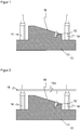
- Figure 1 shows a sectional view of a base part 10 of an electrical device, in particular a sensor.
- the base part 10 is preferably a housing part made of metal or other thermally conductive material, alternatively thermally connected to a housing or another heat sink.
- An electrical component is to be mounted on the base part 10 and cooled by good heat connection, for example an assembled printed circuit board with components such as an FPGA, a microprocessor, a light source or a light receiver, such as one or more photodiodes or APDs (avalanche photodiode) or an image sensor ,
- the base part 10 has an opening 12 for a first fastening element, and depending on the dimensions, several openings 12 for several first fastening elements are also possible. Furthermore, second fastening elements 14 are provided for the electrical component.
- the base part 10 On the upper side, where the electrical component is mounted, the base part 10 has an inclined contact surface 16. In the case of a smooth, horizontal upper side, the electrical component would only be mounted thereon with a large mechanical tolerance, which according to the invention is due to the inclined contact surface 16 and the others, hereinafter with reference to FIG Figures 2 to 6 explained steps for assembling the electrical component is avoided.
- Figure 2 shows a further sectional view of the base part 10, in which a template 18 is placed on the base part 10.
- the second fastening elements 14 are used here, but the template 18 could also be brought into its target position in a different way.
- the template 18 has at least in the later support and fastening areas the same geometry as the electrical component to be assembled, in this example a printed circuit board.
- the ones on the circuit board Electronic components are represented on the template 18 by a material block 18a, which has the dimensions of the electronic components and possibly additionally a heat conducting material to be arranged thereon.
- FIG. 3 shows a further sectional view, in which a wedge element 20, preferably made of metal or another heat-conducting material, is now introduced laterally in such a way that its lower surface rests on the inclined support surface 16.
- a defined lateral force F is exerted, by means of which the wedge element 20 moves into the intermediate space until the lower surface of the wedge element 20 continues to contact the inclined bearing surface 16 and the upper surface of the wedge element 20 to the Template 18 or the material block 18a is pressed.
- the template 18 thus specifies the desired position of the wedge element 20 and, in particular, the height of its upper surface, at which a contact with tolerance compensation is achieved.
- Figure 4 shows a further sectional view, in which the wedge element 20 is fixed to the base part 10 with a first fastening element 22.
- the first fastening element 22 is a screw that is screwed into the opening 12.
- the template 18 can be designed in such a way that a tool access for the fixing of the first fastening element 22 is facilitated, for example by corresponding openings and recesses which the electrical component may not have.
- the direct, vertical application of force of the first fastening element 22 creates an ideal thermal transition between the base part 10 and the wedge element 20.
- the firm pressing on the contact surfaces also makes a conceivable thermal material between base part 10 and wedge element 20 unnecessary.
- Figure 5 shows a sectional view in which, after the wedge element 20 has been fixed to the base part 10 in the desired position for tolerance compensation, the template 18 is removed again. In addition, it is no longer necessary to apply the lateral force.
- Figure 6 shows a sectional view in which the electrical component 24, in this case a printed circuit board equipped with an electronic component 24a, assumes the position fixed with the template 18.
- the electrical component 24 is fixed, in particular screwed, to the base part 10 with the aid of the second fastening elements 14.
- heat-conducting material 26 is preferably also arranged, for example a temperature pad or a heat-conducting paste or both, such as a polyimide film with paste. In this way, remaining tolerances of the electrical component 24 or of the printed circuit board and its assembly can be compensated for.
- a typical expansion of the heat-conducting material 26 can be taken into account in the material block 18a of the template 18.
- the electrical component 24 is placed directly on the base part 10. Then, however, there must be a possibility of fixing the wedge element 20 to the base part 10 with the first fastening element 22 when the electrical component 24 is resting on it. Accessibility can be created, for example, by openings in the electrical component 24 or the printed circuit board, by an overhang of the wedge element 20 with the openings 12, or by a lateral deflection mechanism.
- the one to the Figures 5 and 6 described steps are omitted in this alternative embodiment, it can simply be in the state according to Figure 4 , but replaced with the template 18 by the electrical component 24, the application of the lateral force F can be set.
Landscapes
- Engineering & Computer Science (AREA)
- Microelectronics & Electronic Packaging (AREA)
- Physics & Mathematics (AREA)
- Thermal Sciences (AREA)
- Cooling Or The Like Of Electrical Apparatus (AREA)
- Manufacturing & Machinery (AREA)
- Cooling Or The Like Of Semiconductors Or Solid State Devices (AREA)
Abstract
Description
- Die Erfindung betrifft ein Verfahren zum Montieren eines elektrischen Bauteils auf einem Sockelteil nach dem Oberbegriff von Anspruch 1 sowie eine elektrische Vorrichtung, bei deren Herstellung das Verfahren angewandt ist.
- Die thermische Anbindung von elektrischen Bauteilen ist ein wichtiger Aspekt, der beim Design und bei der Herstellung eines Sensors beachtet werden muss, um dessen Funktion zu gewährleisten. Dabei werden nach Möglichkeit die elektrischen Verbraucher direkt mit dem Sensorgehäuse verbunden, um die Eigenerwärmung des Gerätes so gering wie möglich zu halten. Bei erhöhter Gerätetemperatur drohen Einbußen der Effizienz von optoelektrischen Bauteilen wie Lasern oder LEDs, eine Verschlechterung des Signal-Rausch-Verhältnisses bei Lichtempfängern und Bildsensoren sowie eine verkürzte Lebensdauer. Außerdem müssen die elektrischen Bauteile im spezifizierten Temperaturbereich betrieben werden.
- Bei der Montage beziehungsweise dem Zusammenbauen treten mechanische Toleranzen auf. Damit besteht die zusätzliche Herausforderung, dass die Temperaturanbindung der elektrischen Bauteile durch solche Toleranzen möglichst nicht beeinträchtigt werden sollte.
- Eine herkömmliche Möglichkeit, mit solchen Toleranzen umzugehen, ist eine individuelle Behandlung von Gerät zu Gerät bei der Montage. Dazu werden die Komponenten zunächst ohne Wärmeübergangsmaterial zusammengebaut, und der Abstand zwischen elektrischem Bauteil und Wärmesenke wird vermessen. Dann werden die Komponenten wieder auseinandergebaut, über ein anhand des gemessenen Abstands ausgewähltes Kupferblech werden die großen Toleranzen ausgeglichen, und eine dünne Wärmeleitfolie wird ergänzt, ehe die Bauteile dann verschraubt werden. Die Kupferbleche liegen in gestaffelter Dicke vor. Ein solcher individueller Prozess ist sehr aufwändig und zudem fehleranfällig.
- Eine andere Möglichkeit, um mechanische Toleranzen bei guter Wärmeanbindung auszugleichen, sind Wärmeleitrohre (Heatpipes), die aber ebenfalls mit relativ hohen Kosten verbunden sind.
- Die
US 2017/0363371 A1 offenbart ein selbstausrichtendes Kühlmodul mit zwei Keilen, die mit einem festen thermischen Anbindungsmaterial dazwischen aufeinanderliegen. Eine Feder drückt seitlich gegen einen der Keile, dadurch verklemmen sich die beiden Keile unter Ausgleich von Toleranzen zwischen einer oben befindlichen elektronischen Komponente und einer unten angeordneten Wärmesenke. Das hat aber einige Nachteile: Durch die indirekte seitliche Krafteinwirkung mittels der Feder ist der thermische Übergang zwischen den Keilen beeinträchtigt, und über den Hebel der Keile wird die Wärmesenke ständig mechanisch belastet. Wegen der beiden Keile muss der Temperaturfluss von der elektronischen Komponente bis zur Wärmesenke mehrere Schnittstellen überwinden. Es ist eine langzeitstabile Feder erforderlich, die über die ganze Lebensdauer eine definierte Kraft ausübt. - Es ist daher Aufgabe der Erfindung, die Montage eines elektrischen Bauteils zu verbessern.
- Diese Aufgabe wird durch ein Verfahren zum Montieren eines elektrischen Bauteils auf einem Sockelteil nach Anspruch 1 sowie eine elektrische Vorrichtung nach Anspruch 10 gelöst. Das Sockelteil 10 hat eine schräge Auflagefläche, und darauf wird ein Keilelement mit einer ersten Keilfläche angeordnet. Auf dieses Keilelement wird nun eine seitliche Kraft ausgeübt. Die Kraft wirkt von der Schmalseite des Keilelements her, so dass eine Kraftkomponente das Keilelement sich auf der Auflagefläche nach oben bewegen lässt, bis eine der ersten Keilfläche gegenüberliegende zweite Keilfläche des Keilelements eine gewünschte Position erreicht. Das elektrische Bauteil wird auf der zweiten Keilfläche angeordnet. Anschaulich ausgedrückt bewegt sich das Keilelement so lange auf der Schräge, bis seine Oberseite auf einer gewünschten Höhe für den Kontakt mit der elektrischen Komponente liegt. Dazu entspricht vorzugsweise der Keilwinkel des Keilelements gerade dem Winkel der schrägen Auflagefläche, damit die zweite Keilfläche horizontal orientiert ist.
- Die Erfindung geht von dem Grundgedanken aus, den Toleranzausgleich über das Keilelement nur einmal während der Montage vorzunehmen und dann die erreichte Position festzuhalten. Dazu wird das Keilelement, wenn die zweite Keilfläche die gewünschte Position erreicht hat, mit mindestens einem ersten Befestigungselement an dem Sockelteil fixiert, insbesondere mit einer oder mehreren Schrauben. Anschließend wird die seitliche Kraft nicht mehr ausgeübt. Das Keilelement wird durch das erste Befestigungselement in der gewünschten Lage gehalten, Mittel zur seitlichen Krafteinwirkung mit Auffinden einer gewünschten Position sind deshalb nur während des Zusammenbaus erforderlich, danach nicht mehr.
- Die Erfindung hat den Vorteil, dass mechanische Toleranzen zur verbesserten thermischen Anbindung des elektrischen Bauteils auf einfache Weise ausgeglichen werden. Es ist weder erforderlich, zum Toleranzausgleich dicke Wärmeleitpads mit schlechtem thermischem Leitwert einzusetzen, noch individuell für jedes Gerät ein Wärmeleitblech spezifischer Dicke auszuwählen und einzulegen. Der Wärmefluss über das eine Keilelement ist gut, und die Fixierung ist mit einfachsten Befestigungsmitteln wie Schrauben langzeitstabil.
- Das elektrische Bauteil weist bevorzugt eine Leiterplatte auf. Die Leiterplatte ist mit einem oder mehreren elektrischen Bauteilen bestückt, deren Wärme abgeführt werden soll. Die auszugleichenden mechanischen Toleranzen treten beispielsweise durch das Stapeln von Leiterplatten auf.
- Das Sockelteil ist bevorzugt als Gehäuseteil ausgebildet. Damit kann es die Wärme direkt nach außen ableiten. Alternativ ist das Sockelteil vorzugsweise zumindest thermisch an ein Gehäuseteil angebunden.
- Das Keilelement und/oder das Sockelteil weisen bevorzugt wärmeleitendes Material auf. Dazu sind sie insbesondere aus Metall hergestellt. Es entsteht eine gute Wärmebrücke von dem elektrischen Bauteil nach außen.
- Das Keilelement liegt bevorzugt direkt auf dem Sockelteil auf. Es befinden sich also keine weiteren Bauteile dazwischen, insbesondere kein herkömmlich zum Ausgleich von Toleranzen vorzusehendes Wärmeleitpad. Das ist nicht erforderlich, weil das Keilelement dessen Aufgabe durch Einnehmen der gewünschten Position bereits erfüllt. Vorzugsweise wird wärmeleitendes Material zwischen dem elektrischen Bauteil und der zweiten Keilfläche angeordnet. Während die erste Keilfläche auf dem Sockelteil fixiert und auf diese Weise eine dichte Anbindung sichergestellt ist, kann wärmeleitendes Material an der Schnittstelle zwischen Keil und elektrischem Bauteil helfen, weitere Toleranzen auszugleichen, die thermische Anbindung nochmals zu verbessern und mechanische Belastungen des möglicherweise empfindlichen elektrischen Bauteils zu vermeiden. Dabei geht es aber nur noch um kleine Toleranzen und daher eine dünne Schicht des wärmeleitenden Materials, da der größere Anteil bereits durch den Keil ausgeglichen ist.
- Das erste Befestigungselement bildet vorzugsweise eine zu der Auflagefläche und der ersten Keilfläche senkrechte Verbindung. Es wird also für eine direkte, senkrechte Verbindung und Krafteinwirkung zwischen Keilelement und Sockelteil mit entsprechend gutem thermischem Übergang gesorgt. Das könnte die seitliche Kraft nicht leisten, sie hat nur eine Teilkomponente in dieser während der Lebenszeit des montierten Geräts wesentlichen Richtung. Eine einfache Realisierungsmöglichkeit ist ein selbst senkrecht orientiertes erstes Befestigungselement, insbesondere ein senkrechtes Verschrauben. Eine gewisse Schräglage beispielsweise zur besseren Zugänglichkeit mit einem Werkzeug ist aber noch möglich.
- Das elektrische Bauteil wird bevorzugt auf dem Sockelteil angeordnet, um während des Ausübens der seitlichen Kraft die gewünschte Position vorzugeben. Auf diese Weise gibt das elektrische Bauteil selbst, das in seine Zielposition gebracht wird, die gewünschte Position des Keilelements vor. Die seitliche Kraft drückt es unter Ausgleich der Toleranzen mit der zweiten Keilfläche nach oben bis an die Unterseite des elektrischen Bauteils oder, falls gewünscht, eines dazwischen noch angeordneten Wärmeleitmaterials. In dieser Position wird dann das Keilelement an dem Sockelteil fixiert. Vorzugsweise weist das elektrische Bauteil mindestens eine Öffnung auf, durch die hindurch das erste Befestigungselement fixiert wird. Alternativ kann das Keilelement seitliche Befestigungsbereiche aufweisen, die für ein Werkzeug zum Fixieren des ersten Befestigungselements zugänglich bleiben.
- Vorzugsweise wird zunächst vor dem elektrischen Bauteil eine Schablone mit einer Geometrie entsprechend dem elektrischen Bauteil auf dem Sockelteil angeordnet, um während des Ausübens der seitlichen Kraft die gewünschte Position vorzugeben. Der Schablone schaden gewisse mechanische Belastungen während des Toleranzausgleichs mit der seitlichen Kraft und der Fixierung des Keilelements nicht, die ein elektrisches Bauteil wie eine bestückte Leiterplatte beeinträchtigen könnten. Außerdem kann die Schablone so ausgelegt sein, dass es einen einfachen Zugang für das Fixieren des ersten Befestigungselements gibt. Die Übereinstimmung der Geometrie der Schablone mit derjenigen des elektrischen Bauteils betrifft nur die Bereiche, die für die Auflage auf der zweiten Keilfläche und die Befestigung auf dem Sockelteil relevant sind, so dass ansonsten Freiheit besteht, Öffnungen und dergleichen für den Werkzeugzugang vorzusehen.
- Die Schablone wird dann vorzugsweise entfernt, wenn das Keilelement mit dem ersten Befestigungselement an dem Sockelteil fixiert ist. Statt der Schablone wird das elektrische Bauteil mit mindestens einem zweiten Befestigungselement an dem Sockelteil fixiert, insbesondere verschraubt. Im Falle einer Leiterplatte liegen nun die bestückten elektrischen Komponenten auf der zweiten Keilfläche auf, wie dies mit der Schablone ausgemessen wurde, und so wird deren Abwärme durch das Keilelement in das Sockelteil und weiter nach außen abgeführt. Die Schablone kann einen definierten Abstand für ein Wärmeleitpad oder dergleichen zwischen dem elektrischen Bauteil und dem zweiten Keilelement berücksichtigen.
- In bevorzugter Weiterbildung wird ein Verfahren zur Herstellung eines Sensors angegeben, bei dem mit einer der Ausführungsformen des erfindungsgemäßen Verfahrens mindestens ein elektrisches Bauteil auf mindestens einem Sockelteil montiert wird. Der Sensor ist bevorzugt ein optoelektronischer Sensor, insbesondere eine Kamera, die als Codeleser ausgebildet sein kann. Das elektrische Bauteil kann eine Leiterplatte mit einer Lichtquelle, einem Lichtempfänger oder Bildsensor und sonstigen elektronischen Komponenten für Datenaustausch, Versorgung oder Steuer- beziehungsweise Auswertungsfunktionen sein.
- In einer erfindungsgemäßen elektrischen Vorrichtung, insbesondere einem Sensor der im Vorabsatz genannten Art, ist mindestens ein elektrisches Bauteil auf mindestens einem Sockelteil des Sensors mit einem Keilelement dazwischen nach dem erfindungsgemäßen Verfahren montiert.
- Die Erfindung wird nachstehend auch hinsichtlich weiterer Merkmale und Vorteile beispielhaft anhand von Ausführungsformen und unter Bezug auf die beigefügte Zeichnung näher erläutert. Die Abbildungen der Zeichnung zeigen in:
- Fig. 1
- eine Schnittdarstellung eines Sockelteils mit schräger Auflagefläche;
- Fig. 2
- eine Schnittdarstellung des Sockelteils mit aufgelegter Schablone eines elektrischen Bauteils;
- Fig. 3
- eine Schnittdarstellung, bei der ein Metallkeil zwischen Sockelteil und Schablone eingeführt und mit einer seitlichen Kraft angedrückt wird;
- Fig. 4
- eine Schnittdarstellung, in welcher der Metallkeil in einer Zielposition fixiert wird;
- Fig. 5
- eine Schnittdarstellung, bei der nach der Fixierung die seitliche Kraft nicht mehr ausgeübt und die Schablone entfernt wird; und
- Fig. 6
- eine Schnittdarstellung, in der das elektrisches Bauteil anstelle der Schablone aufgelegt und an dem Sockelteil befestigt wird.
-
Figur 1 zeigt eine Schnittdarstellung eines Sockelteils 10 einer elektrischen Vorrichtung, insbesondere eines Sensors. Das Sockelteil 10 ist vorzugsweise ein Gehäuseteil aus Metall oder anderem wärmeleitfähigen Material, alternativ thermisch mit einem Gehäuse oder einer anderen Wärmesenke verbunden. Auf dem Sockelteil 10 soll ein elektrisches Bauteil montiert und durch gute Wärmeanbindung gekühlt werden, beispielsweise eine bestückte Leiterplatte mit Komponenten wie einem FPGA, einem Mikroprozessor, einer Lichtquelle oder einem Lichtempfänger, etwa wie eine oder mehrere Photodioden oder APDs (Avalanche Photodiode) oder ein Bildsensor. - Das Sockelteil 10 hat eine Öffnung 12 für ein erstes Befestigungselement, wobei je nach Abmessungen auch mehrere Öffnungen 12 für mehrere erste Befestigungselemente möglich sind. Ferner sind zweite Befestigungselemente 14 für das elektrische Bauteil vorgesehen. Auf der Oberseite, wo das elektrische Bauteil montiert wird, weist das Sockelteil 10 eine schräge Auflagefläche 16 auf. Bei glatter, horizontaler Oberseite würde das elektrische Bauteil darauf nur mit großer mechanischer Toleranz montiert, die erfindungsgemäß durch die schräge Auflagefläche 16 und die weiteren, nachfolgend unter Bezugnahme auf die
Figuren 2 bis 6 erläuterten Schritte zur Montage des elektrischen Bauteils vermieden wird. -
Figur 2 zeigt eine weitere Schnittdarstellung des Sockelteils 10, in der eine Schablone 18 auf das Sockelteil 10 aufgelegt wird. Dazu werden hier die zweiten Befestigungselemente 14 genutzt, aber die Schablone 18 könnte auch anders in ihre Zielposition gebracht werden. Die Schablone 18 weist zumindest in den späteren Auflage- und Befestigungsbereichen dieselbe Geometrie auf wie das zu montierende elektrische Bauteil, in diesem Beispiel eine bestückte Leiterplatte. Die auf der Leiterplatte befindlichen elektronischen Komponenten werden auf der Schablone 18 durch einen Materialblock 18a repräsentiert, welcher die Abmessungen der elektronischen Komponenten und möglicherweise zusätzlich eines darauf anzuordnenden Wärmeleitmaterials hat. -
Figur 3 zeigt eine weitere Schnittansicht, in der nun ein Keilelement 20 vorzugsweise aus Metall oder einem anderen wärmeleitenden Material seitlich so eingeführt wird, dass es mit seiner unteren Fläche auf der schrägen Auflagefläche 16 aufliegt. Von der Schmalseite des Keilelements 20 her wird eine definierte seitliche Kraft F ausgeübt, durch die sich das Keilelement 20 so weit in den Zwischenraum bewegt, bis die untere Fläche des Keilelements 20 weiterhin an die schräge Auflagefläche 16 und die obere Fläche des Keilelements 20 an die Schablone 18 beziehungsweise den Materialblock 18a angedrückt ist. Die Schablone 18 gibt somit die gewünschte Position des Keilelements 20 und insbesondere die Höhe von dessen oberer Fläche vor, bei der ein Aufliegen unter Toleranzausgleich erreicht ist. -
Figur 4 zeigt eine weitere Schnittansicht, in welcher das Keilelement 20 mit einem ersten Befestigungselement 22 an dem Sockelteil 10 fixiert wird. In diesem Beispiel ist das erste Befestigungselement 22 eine Schraube, die in die Öffnung 12 eingeschraubt wird. Die Schablone 18 kann so ausgelegt sein, dass ein Werkzeugzugang für die Fixierung des ersten Befestigungselements 22 erleichtert ist, beispielsweise durch entsprechende Öffnungen und Aussparungen, welche das elektrische Bauteil möglichweise nicht aufweist. Durch die direkte, senkrechte Krafteinwirkung des ersten Befestigungselements 22 ist ein idealer thermischer Übergang zwischen Sockelteil 10 und Keilelement 20 hergestellt. Das feste Andrücken an den Kontaktflächen macht auch ein an sich denkbares Wärmematerial zwischen Sockelteil 10 und Keilelement 20 entbehrlich. -
Figur 5 zeigt eine Schnittansicht, in dem nach Fixierung des Keilelements 20 an dem Sockelteil 10 in der gewünschten Position zum Toleranzausgleich die Schablone 18 wieder entfernt ist. Außerdem ist nun das Einwirken der seitlichen Kraft nicht länger erforderlich. -
Figur 6 zeigt eine Schnittansicht, in der das elektrische Bauteil 24, in diesem Fall eine mit einer elektronischen Komponente 24a bestückte Leiterplatte, die mit der Schablone 18 festgelegte Position einnimmt. Das elektrische Bauteil 24 wird mit Hilfe der zweiten Befestigungselemente 14 an dem Sockelteil 10 fixiert, insbesondere verschraubt. Zwischen dem elektrischen Bauteil 24 und dem Keilelement 20 ist vorzugsweise noch wärmeleitendes Material 26 angeordnet, beispielsweise ein Temperaturpad oder eine Wärmeleitpaste oder beides, wie eine Polyimid-Folie mit Paste. Damit können verbleibende Toleranzen des elektrischen Bauteils 24 beziehungsweise der Leiterplatte und deren Bestückung ausgeglichen werden. Eine typische Ausdehnung des wärmeleitenden Materials 26 kann in dem Materialblock 18a der Schablone 18 berücksichtigt sein. - Alternativ zu einer Höhenanpassung mittels Schablone 18 kann auch im zu
Figur 2 beschriebenen Schritt direkt das elektrische Bauteil 24 auf das Sockelteil 10 aufgelegt werden. Dann muss es aber eine Möglichkeit geben, das Keilelement 20 bei aufliegendem elektrischem Bauteil 24 mit dem ersten Befestigungselement 22 auf dem Sockelteil 10 zu fixieren. Die Zugänglichkeit kann beispielsweise durch Öffnungen in dem elektrischen Bauteil 24 beziehungsweise der Leiterplatte, durch einen Überstand des Keilelements 20 mit den Öffnungen 12 oder über eine seitliche Umlenkmechanik geschaffen werden. Die zu denFiguren 5 und 6 beschriebenen Schritte entfallen in dieser alternativen Ausführungsform, es kann einfach im Zustand gemäßFigur 4 , allerdings mit der Schablone 18 durch das elektrische Bauteil 24 ersetzt, das Ausüben der seitlichen Kraft F eingestellt werden.
Claims (10)
- Verfahren zum Montieren eines elektrischen Bauteils (24) auf einem Sockelteil (10) mit einer schrägen Auflagefläche (16), bei dem ein Keilelement (20) mit einer ersten Keilfläche auf der Auflagefläche (16) angeordnet und eine seitliche Kraft (F) auf das Keilelement (20) ausgeübt wird, so dass sich die erste Keilfläche auf der Auflagefläche (16) bewegt, bis eine von der Auflagefläche (16) abgewandte zweite Keilfläche des Keilelements (20) eine gewünschte Position erreicht, und wobei das elektrische Bauteil (24) auf der zweiten Keilfläche angeordnet wird,
dadurch gekennzeichnet,
dass das Keilelement (20) mit einem ersten Befestigungselement (20) an dem Sockelteil (10) fixiert wird und danach die seitliche Kraft (F) nicht mehr ausgeübt wird. - Verfahren nach Anspruch 1,
wobei das elektrische Bauteil (24) eine Leiterplatte aufweist und/oder wobei das Sockelteil (10) als Gehäuseteil ausgebildet ist. - Verfahren nach Anspruch 1 oder 2,
wobei das Keilelement (20) und/oder das Sockelteil (10) wärmeleitendes Material aufweisen. - Verfahren nach einem der vorhergehenden Ansprüche,
wobei das Keilelement (20) direkt auf dem Sockelteil (10) aufliegt. - Verfahren nach einem der vorhergehenden Ansprüche,
wobei wärmeleitendes Material (26) zwischen dem elektrischen Bauteil (24) und der zweiten Keilfläche angeordnet wird. - Verfahren nach einem der vorhergehenden Ansprüche,
wobei das erste Befestigungselement (22) eine zu der Auflagefläche (16) und der ersten Keilfläche senkrechte Verbindung bildet. - Verfahren nach einem der vorhergehenden Ansprüche,
wobei das elektrische Bauteil (24) auf dem Sockelteil (10) angeordnet wird, um während des Ausübens der seitlichen Kraft (F) die gewünschte Position vorzugeben. - Verfahren nach einem der Ansprüche 1 bis 6,
wobei zunächst vor dem elektrischen Bauteil (24) eine Schablone (18) mit einer Geometrie entsprechend dem elektrischen Bauteil (24) auf dem Sockelteil (10) angeordnet wird, um während des Ausübens der seitlichen Kraft (F) die gewünschte Position vorzugeben, und wobei insbesondere die Schablone (18) entfernt wird, wenn das Keilelement (20) mit dem ersten Befestigungselement (22) an dem Sockelteil (10) fixiert ist. - Verfahren zur Herstellung eines Sensors, bei dem mit einem Verfahren nach einem der vorhergehenden Ansprüche mindestens ein elektrisches Bauteil (24) auf mindestens einem Sockelteil (10) montiert wird.
- Elektrische Vorrichtung, insbesondere optoelektrischer Sensor, mit mindestens einem elektrischen Bauteil (24) und mindestens einem Sockelteil (10), wobei das elektrische Bauteil (24) mit einem Keilelement (20) dazwischen mit einem Verfahren nach einem der Ansprüche 1 bis 8 auf dem Sockelteil (10) montiert ist.
Applications Claiming Priority (1)
| Application Number | Priority Date | Filing Date | Title |
|---|---|---|---|
| DE102018117695.3A DE102018117695B3 (de) | 2018-07-23 | 2018-07-23 | Verfahren zum Montieren eines elektrischen Bauteils auf einem Sockelteil |
Publications (2)
| Publication Number | Publication Date |
|---|---|
| EP3599806A1 true EP3599806A1 (de) | 2020-01-29 |
| EP3599806B1 EP3599806B1 (de) | 2020-12-30 |
Family
ID=67137575
Family Applications (1)
| Application Number | Title | Priority Date | Filing Date |
|---|---|---|---|
| EP19183152.8A Active EP3599806B1 (de) | 2018-07-23 | 2019-06-28 | Verfahren zum montieren eines elektrischen bauteils auf einem sockelteil |
Country Status (4)
| Country | Link |
|---|---|
| US (1) | US10971639B2 (de) |
| EP (1) | EP3599806B1 (de) |
| DE (1) | DE102018117695B3 (de) |
| DK (1) | DK3599806T3 (de) |
Citations (6)
| Publication number | Priority date | Publication date | Assignee | Title |
|---|---|---|---|---|
| DE8711779U1 (de) * | 1987-08-31 | 1987-11-19 | Siemens AG, 1000 Berlin und 8000 München | Wärmeleiter für Bauelemente der elektrischen Nachrichtentechnik |
| US20050047092A1 (en) * | 2003-08-25 | 2005-03-03 | Whit Joseph M. | Method of assembly of a wedge thermal interface to allow expansion after assembly |
| DE102006037747A1 (de) * | 2006-08-11 | 2008-03-13 | Nokia Siemens Networks Gmbh & Co.Kg | Anordnung zur Kühlung eines elektrischen Bauelements |
| DE102007049035A1 (de) * | 2007-10-11 | 2009-04-23 | GE Fanuc Intelligent Platforms Embedded Systems, Inc. (n.d.Ges.d. Staates Delaware) | Chipkühlvorrichtung mit Keilelement |
| US20140133093A1 (en) * | 2012-11-15 | 2014-05-15 | International Business Machines Corporation | Cooling system for electronics |
| US20170363371A1 (en) | 2016-06-15 | 2017-12-21 | Mellanox Technologies Ltd. | Self-adjusting cooling module |
Family Cites Families (4)
| Publication number | Priority date | Publication date | Assignee | Title |
|---|---|---|---|---|
| US5472353A (en) | 1995-04-13 | 1995-12-05 | Hristake; Val | Isobaric expandable thermal clamp for printed circuit board |
| US6985359B2 (en) * | 2003-04-21 | 2006-01-10 | Hewlett-Packard Development Company, L.P. | Variable-wedge thermal-interface device |
| US20130003316A1 (en) | 2010-12-28 | 2013-01-03 | Elma Electronic Inc. | Card Lock Retainer For Pluggable Conduction Cooled Circuit Card Assemblies |
| TWI564535B (zh) | 2015-02-16 | 2017-01-01 | 國立清華大學 | 快速拆卸式之散熱連接裝置 |
-
2018
- 2018-07-23 DE DE102018117695.3A patent/DE102018117695B3/de not_active Expired - Fee Related
-
2019
- 2019-06-28 EP EP19183152.8A patent/EP3599806B1/de active Active
- 2019-06-28 DK DK19183152.8T patent/DK3599806T3/da active
- 2019-07-09 US US16/506,025 patent/US10971639B2/en active Active
Patent Citations (6)
| Publication number | Priority date | Publication date | Assignee | Title |
|---|---|---|---|---|
| DE8711779U1 (de) * | 1987-08-31 | 1987-11-19 | Siemens AG, 1000 Berlin und 8000 München | Wärmeleiter für Bauelemente der elektrischen Nachrichtentechnik |
| US20050047092A1 (en) * | 2003-08-25 | 2005-03-03 | Whit Joseph M. | Method of assembly of a wedge thermal interface to allow expansion after assembly |
| DE102006037747A1 (de) * | 2006-08-11 | 2008-03-13 | Nokia Siemens Networks Gmbh & Co.Kg | Anordnung zur Kühlung eines elektrischen Bauelements |
| DE102007049035A1 (de) * | 2007-10-11 | 2009-04-23 | GE Fanuc Intelligent Platforms Embedded Systems, Inc. (n.d.Ges.d. Staates Delaware) | Chipkühlvorrichtung mit Keilelement |
| US20140133093A1 (en) * | 2012-11-15 | 2014-05-15 | International Business Machines Corporation | Cooling system for electronics |
| US20170363371A1 (en) | 2016-06-15 | 2017-12-21 | Mellanox Technologies Ltd. | Self-adjusting cooling module |
Also Published As
| Publication number | Publication date |
|---|---|
| EP3599806B1 (de) | 2020-12-30 |
| DK3599806T3 (da) | 2021-03-01 |
| US10971639B2 (en) | 2021-04-06 |
| DE102018117695B3 (de) | 2019-09-26 |
| US20200027998A1 (en) | 2020-01-23 |
Similar Documents
| Publication | Publication Date | Title |
|---|---|---|
| EP0873673B1 (de) | Steuergerät bestehend aus mindestens zwei gehäuseteilen | |
| EP0854666B1 (de) | Steuergerät bestehend aus mindestens zwei Gehäuseteilen | |
| DE69400105T2 (de) | Befestigungsteil mit geneigter Spiralfeder für Wärmesenke für ein elektronisches Bauelement | |
| DE112015002430T5 (de) | Schaltungsbaugruppe und elektrischer Verteiler | |
| WO2023083823A1 (de) | Leiterplattenanordnung | |
| EP1503615A2 (de) | Leiterplatine mit gekühltem Baustein, insbesondere SMD-Baustein | |
| DE102005049872B4 (de) | IC-Bauelement mit Kühlanordnung | |
| WO2005015970A2 (de) | Kühlvorrichtung für ein elektronisches bauelement, insbesondere für einen mikroprozessor | |
| EP2122680A1 (de) | Transistorklemmvorrichtung | |
| DE202013002411U1 (de) | Wärmeverteiler mit Flachrohrkühlelement | |
| EP1887621A2 (de) | Leistungselektronik mit Kühlkörper | |
| WO2016026749A1 (de) | Optisches modul mit objektivträger und wärmeleitend kontaktierter leiterplatte | |
| EP1791177A1 (de) | Halbleitereinheit mit verbesserter Wärmekopplungsanordnung | |
| WO2008083878A1 (de) | Fixierungselement für leiterplatten | |
| EP3599806B1 (de) | Verfahren zum montieren eines elektrischen bauteils auf einem sockelteil | |
| EP0652694B1 (de) | Steuergerät für ein Kraftfahrzeug | |
| DE102006056793B4 (de) | Elektronikvorrichtung und Verfahren zum Herstellen derselben | |
| EP4533916A1 (de) | Leiterplattenanordnung | |
| DE112019002508T5 (de) | Schaltungseinrichtung | |
| DE10064221B4 (de) | Leiterplatine mit gekühltem SMD-Baustein | |
| DE112018008124T5 (de) | Thermische schnittstelleneinrichtung für gedruckte pci express m.2-schaltungsanordnungen | |
| WO2013153008A1 (de) | Befestigungsanordnung zur befestigung eines gehäuses eines led-moduls | |
| DE102005012147A1 (de) | Vorrichtung zum Herstellen einer thermischen und mechanischen Verbindung | |
| WO2006102875A2 (de) | Leiterplattenanordnung | |
| EP1470586B1 (de) | Leistungs-halbleiter, und verfahen zu seiner herstellung |
Legal Events
| Date | Code | Title | Description |
|---|---|---|---|
| PUAI | Public reference made under article 153(3) epc to a published international application that has entered the european phase |
Free format text: ORIGINAL CODE: 0009012 |
|
| STAA | Information on the status of an ep patent application or granted ep patent |
Free format text: STATUS: THE APPLICATION HAS BEEN PUBLISHED |
|
| AK | Designated contracting states |
Kind code of ref document: A1 Designated state(s): AL AT BE BG CH CY CZ DE DK EE ES FI FR GB GR HR HU IE IS IT LI LT LU LV MC MK MT NL NO PL PT RO RS SE SI SK SM TR |
|
| AX | Request for extension of the european patent |
Extension state: BA ME |
|
| RAP1 | Party data changed (applicant data changed or rights of an application transferred) |
Owner name: SICK AG |
|
| STAA | Information on the status of an ep patent application or granted ep patent |
Free format text: STATUS: REQUEST FOR EXAMINATION WAS MADE |
|
| 17P | Request for examination filed |
Effective date: 20200317 |
|
| RBV | Designated contracting states (corrected) |
Designated state(s): AL AT BE BG CH CY CZ DE DK EE ES FI FR GB GR HR HU IE IS IT LI LT LU LV MC MK MT NL NO PL PT RO RS SE SI SK SM TR |
|
| STAA | Information on the status of an ep patent application or granted ep patent |
Free format text: STATUS: EXAMINATION IS IN PROGRESS |
|
| 17Q | First examination report despatched |
Effective date: 20200527 |
|
| GRAP | Despatch of communication of intention to grant a patent |
Free format text: ORIGINAL CODE: EPIDOSNIGR1 |
|
| STAA | Information on the status of an ep patent application or granted ep patent |
Free format text: STATUS: GRANT OF PATENT IS INTENDED |
|
| INTG | Intention to grant announced |
Effective date: 20201006 |
|
| GRAS | Grant fee paid |
Free format text: ORIGINAL CODE: EPIDOSNIGR3 |
|
| GRAA | (expected) grant |
Free format text: ORIGINAL CODE: 0009210 |
|
| STAA | Information on the status of an ep patent application or granted ep patent |
Free format text: STATUS: THE PATENT HAS BEEN GRANTED |
|
| AK | Designated contracting states |
Kind code of ref document: B1 Designated state(s): AL AT BE BG CH CY CZ DE DK EE ES FI FR GB GR HR HU IE IS IT LI LT LU LV MC MK MT NL NO PL PT RO RS SE SI SK SM TR |
|
| REG | Reference to a national code |
Ref country code: GB Ref legal event code: FG4D Free format text: NOT ENGLISH |
|
| REG | Reference to a national code |
Ref country code: DE Ref legal event code: R096 Ref document number: 502019000606 Country of ref document: DE |
|
| REG | Reference to a national code |
Ref country code: AT Ref legal event code: REF Ref document number: 1351279 Country of ref document: AT Kind code of ref document: T Effective date: 20210115 |
|
| REG | Reference to a national code |
Ref country code: IE Ref legal event code: FG4D Free format text: LANGUAGE OF EP DOCUMENT: GERMAN |
|
| REG | Reference to a national code |
Ref country code: DK Ref legal event code: T3 Effective date: 20210222 |
|
| REG | Reference to a national code |
Ref country code: SE Ref legal event code: TRGR |
|
| REG | Reference to a national code |
Ref country code: NL Ref legal event code: FP |
|
| PG25 | Lapsed in a contracting state [announced via postgrant information from national office to epo] |
Ref country code: NO Free format text: LAPSE BECAUSE OF FAILURE TO SUBMIT A TRANSLATION OF THE DESCRIPTION OR TO PAY THE FEE WITHIN THE PRESCRIBED TIME-LIMIT Effective date: 20210330 Ref country code: GR Free format text: LAPSE BECAUSE OF FAILURE TO SUBMIT A TRANSLATION OF THE DESCRIPTION OR TO PAY THE FEE WITHIN THE PRESCRIBED TIME-LIMIT Effective date: 20210331 Ref country code: RS Free format text: LAPSE BECAUSE OF FAILURE TO SUBMIT A TRANSLATION OF THE DESCRIPTION OR TO PAY THE FEE WITHIN THE PRESCRIBED TIME-LIMIT Effective date: 20201230 Ref country code: FI Free format text: LAPSE BECAUSE OF FAILURE TO SUBMIT A TRANSLATION OF THE DESCRIPTION OR TO PAY THE FEE WITHIN THE PRESCRIBED TIME-LIMIT Effective date: 20201230 |
|
| PG25 | Lapsed in a contracting state [announced via postgrant information from national office to epo] |
Ref country code: BG Free format text: LAPSE BECAUSE OF FAILURE TO SUBMIT A TRANSLATION OF THE DESCRIPTION OR TO PAY THE FEE WITHIN THE PRESCRIBED TIME-LIMIT Effective date: 20210330 Ref country code: LV Free format text: LAPSE BECAUSE OF FAILURE TO SUBMIT A TRANSLATION OF THE DESCRIPTION OR TO PAY THE FEE WITHIN THE PRESCRIBED TIME-LIMIT Effective date: 20201230 |
|
| PG25 | Lapsed in a contracting state [announced via postgrant information from national office to epo] |
Ref country code: HR Free format text: LAPSE BECAUSE OF FAILURE TO SUBMIT A TRANSLATION OF THE DESCRIPTION OR TO PAY THE FEE WITHIN THE PRESCRIBED TIME-LIMIT Effective date: 20201230 |
|
| REG | Reference to a national code |
Ref country code: LT Ref legal event code: MG9D |
|
| PG25 | Lapsed in a contracting state [announced via postgrant information from national office to epo] |
Ref country code: CZ Free format text: LAPSE BECAUSE OF FAILURE TO SUBMIT A TRANSLATION OF THE DESCRIPTION OR TO PAY THE FEE WITHIN THE PRESCRIBED TIME-LIMIT Effective date: 20201230 Ref country code: SK Free format text: LAPSE BECAUSE OF FAILURE TO SUBMIT A TRANSLATION OF THE DESCRIPTION OR TO PAY THE FEE WITHIN THE PRESCRIBED TIME-LIMIT Effective date: 20201230 Ref country code: EE Free format text: LAPSE BECAUSE OF FAILURE TO SUBMIT A TRANSLATION OF THE DESCRIPTION OR TO PAY THE FEE WITHIN THE PRESCRIBED TIME-LIMIT Effective date: 20201230 Ref country code: LT Free format text: LAPSE BECAUSE OF FAILURE TO SUBMIT A TRANSLATION OF THE DESCRIPTION OR TO PAY THE FEE WITHIN THE PRESCRIBED TIME-LIMIT Effective date: 20201230 Ref country code: PT Free format text: LAPSE BECAUSE OF FAILURE TO SUBMIT A TRANSLATION OF THE DESCRIPTION OR TO PAY THE FEE WITHIN THE PRESCRIBED TIME-LIMIT Effective date: 20210430 Ref country code: RO Free format text: LAPSE BECAUSE OF FAILURE TO SUBMIT A TRANSLATION OF THE DESCRIPTION OR TO PAY THE FEE WITHIN THE PRESCRIBED TIME-LIMIT Effective date: 20201230 |
|
| PG25 | Lapsed in a contracting state [announced via postgrant information from national office to epo] |
Ref country code: PL Free format text: LAPSE BECAUSE OF FAILURE TO SUBMIT A TRANSLATION OF THE DESCRIPTION OR TO PAY THE FEE WITHIN THE PRESCRIBED TIME-LIMIT Effective date: 20201230 |
|
| PG25 | Lapsed in a contracting state [announced via postgrant information from national office to epo] |
Ref country code: IS Free format text: LAPSE BECAUSE OF FAILURE TO SUBMIT A TRANSLATION OF THE DESCRIPTION OR TO PAY THE FEE WITHIN THE PRESCRIBED TIME-LIMIT Effective date: 20210430 |
|
| REG | Reference to a national code |
Ref country code: DE Ref legal event code: R097 Ref document number: 502019000606 Country of ref document: DE |
|
| PG25 | Lapsed in a contracting state [announced via postgrant information from national office to epo] |
Ref country code: AL Free format text: LAPSE BECAUSE OF FAILURE TO SUBMIT A TRANSLATION OF THE DESCRIPTION OR TO PAY THE FEE WITHIN THE PRESCRIBED TIME-LIMIT Effective date: 20201230 |
|
| PLBE | No opposition filed within time limit |
Free format text: ORIGINAL CODE: 0009261 |
|
| STAA | Information on the status of an ep patent application or granted ep patent |
Free format text: STATUS: NO OPPOSITION FILED WITHIN TIME LIMIT |
|
| 26N | No opposition filed |
Effective date: 20211001 |
|
| PG25 | Lapsed in a contracting state [announced via postgrant information from national office to epo] |
Ref country code: ES Free format text: LAPSE BECAUSE OF FAILURE TO SUBMIT A TRANSLATION OF THE DESCRIPTION OR TO PAY THE FEE WITHIN THE PRESCRIBED TIME-LIMIT Effective date: 20201230 Ref country code: MC Free format text: LAPSE BECAUSE OF FAILURE TO SUBMIT A TRANSLATION OF THE DESCRIPTION OR TO PAY THE FEE WITHIN THE PRESCRIBED TIME-LIMIT Effective date: 20201230 |
|
| PG25 | Lapsed in a contracting state [announced via postgrant information from national office to epo] |
Ref country code: SI Free format text: LAPSE BECAUSE OF FAILURE TO SUBMIT A TRANSLATION OF THE DESCRIPTION OR TO PAY THE FEE WITHIN THE PRESCRIBED TIME-LIMIT Effective date: 20201230 |
|
| REG | Reference to a national code |
Ref country code: BE Ref legal event code: MM Effective date: 20210630 |
|
| PG25 | Lapsed in a contracting state [announced via postgrant information from national office to epo] |
Ref country code: LU Free format text: LAPSE BECAUSE OF NON-PAYMENT OF DUE FEES Effective date: 20210628 |
|
| PG25 | Lapsed in a contracting state [announced via postgrant information from national office to epo] |
Ref country code: IE Free format text: LAPSE BECAUSE OF NON-PAYMENT OF DUE FEES Effective date: 20210628 |
|
| PG25 | Lapsed in a contracting state [announced via postgrant information from national office to epo] |
Ref country code: IS Free format text: LAPSE BECAUSE OF FAILURE TO SUBMIT A TRANSLATION OF THE DESCRIPTION OR TO PAY THE FEE WITHIN THE PRESCRIBED TIME-LIMIT Effective date: 20210430 |
|
| PG25 | Lapsed in a contracting state [announced via postgrant information from national office to epo] |
Ref country code: BE Free format text: LAPSE BECAUSE OF NON-PAYMENT OF DUE FEES Effective date: 20210630 |
|
| PG25 | Lapsed in a contracting state [announced via postgrant information from national office to epo] |
Ref country code: CY Free format text: LAPSE BECAUSE OF FAILURE TO SUBMIT A TRANSLATION OF THE DESCRIPTION OR TO PAY THE FEE WITHIN THE PRESCRIBED TIME-LIMIT Effective date: 20201230 |
|
| PG25 | Lapsed in a contracting state [announced via postgrant information from national office to epo] |
Ref country code: SM Free format text: LAPSE BECAUSE OF FAILURE TO SUBMIT A TRANSLATION OF THE DESCRIPTION OR TO PAY THE FEE WITHIN THE PRESCRIBED TIME-LIMIT Effective date: 20201230 Ref country code: HU Free format text: LAPSE BECAUSE OF FAILURE TO SUBMIT A TRANSLATION OF THE DESCRIPTION OR TO PAY THE FEE WITHIN THE PRESCRIBED TIME-LIMIT; INVALID AB INITIO Effective date: 20190628 |
|
| GBPC | Gb: european patent ceased through non-payment of renewal fee |
Effective date: 20230628 |
|
| PG25 | Lapsed in a contracting state [announced via postgrant information from national office to epo] |
Ref country code: MK Free format text: LAPSE BECAUSE OF FAILURE TO SUBMIT A TRANSLATION OF THE DESCRIPTION OR TO PAY THE FEE WITHIN THE PRESCRIBED TIME-LIMIT Effective date: 20201230 Ref country code: GB Free format text: LAPSE BECAUSE OF NON-PAYMENT OF DUE FEES Effective date: 20230628 |
|
| PG25 | Lapsed in a contracting state [announced via postgrant information from national office to epo] |
Ref country code: MT Free format text: LAPSE BECAUSE OF FAILURE TO SUBMIT A TRANSLATION OF THE DESCRIPTION OR TO PAY THE FEE WITHIN THE PRESCRIBED TIME-LIMIT Effective date: 20201230 |
|
| PGFP | Annual fee paid to national office [announced via postgrant information from national office to epo] |
Ref country code: DE Payment date: 20250618 Year of fee payment: 7 |
|
| PGFP | Annual fee paid to national office [announced via postgrant information from national office to epo] |
Ref country code: DK Payment date: 20250618 Year of fee payment: 7 |
|
| PGFP | Annual fee paid to national office [announced via postgrant information from national office to epo] |
Ref country code: NL Payment date: 20250618 Year of fee payment: 7 |
|
| PGFP | Annual fee paid to national office [announced via postgrant information from national office to epo] |
Ref country code: FR Payment date: 20250618 Year of fee payment: 7 |
|
| PGFP | Annual fee paid to national office [announced via postgrant information from national office to epo] |
Ref country code: AT Payment date: 20250616 Year of fee payment: 7 |
|
| PGFP | Annual fee paid to national office [announced via postgrant information from national office to epo] |
Ref country code: SE Payment date: 20250618 Year of fee payment: 7 |
|
| PGFP | Annual fee paid to national office [announced via postgrant information from national office to epo] |
Ref country code: IT Payment date: 20250630 Year of fee payment: 7 |
|
| PGFP | Annual fee paid to national office [announced via postgrant information from national office to epo] |
Ref country code: CH Payment date: 20250701 Year of fee payment: 7 |
|
| PG25 | Lapsed in a contracting state [announced via postgrant information from national office to epo] |
Ref country code: TR Free format text: LAPSE BECAUSE OF FAILURE TO SUBMIT A TRANSLATION OF THE DESCRIPTION OR TO PAY THE FEE WITHIN THE PRESCRIBED TIME-LIMIT Effective date: 20201230 |