EP3599720B1 - Filtres utilisant des resonateurs couples à ondes acoustiques de surface - Google Patents
Filtres utilisant des resonateurs couples à ondes acoustiques de surface Download PDFInfo
- Publication number
- EP3599720B1 EP3599720B1 EP18306023.5A EP18306023A EP3599720B1 EP 3599720 B1 EP3599720 B1 EP 3599720B1 EP 18306023 A EP18306023 A EP 18306023A EP 3599720 B1 EP3599720 B1 EP 3599720B1
- Authority
- EP
- European Patent Office
- Prior art keywords
- reflecting
- structures
- cavity filter
- coupled cavity
- transducer
- Prior art date
- Legal status (The legal status is an assumption and is not a legal conclusion. Google has not performed a legal analysis and makes no representation as to the accuracy of the status listed.)
- Active
Links
- 238000010897 surface acoustic wave method Methods 0.000 title claims description 34
- 239000000758 substrate Substances 0.000 claims description 78
- 230000008878 coupling Effects 0.000 claims description 37
- 238000010168 coupling process Methods 0.000 claims description 37
- 238000005859 coupling reaction Methods 0.000 claims description 37
- VYPSYNLAJGMNEJ-UHFFFAOYSA-N silicon dioxide Inorganic materials O=[Si]=O VYPSYNLAJGMNEJ-UHFFFAOYSA-N 0.000 claims description 28
- 239000002131 composite material Substances 0.000 claims description 26
- 239000000463 material Substances 0.000 claims description 23
- 229910052710 silicon Inorganic materials 0.000 claims description 16
- 239000010703 silicon Substances 0.000 claims description 15
- 238000002161 passivation Methods 0.000 claims description 10
- 229910012463 LiTaO3 Inorganic materials 0.000 claims description 9
- 229910003327 LiNbO3 Inorganic materials 0.000 claims description 7
- XLOMVQKBTHCTTD-UHFFFAOYSA-N Zinc monoxide Chemical compound [Zn]=O XLOMVQKBTHCTTD-UHFFFAOYSA-N 0.000 claims description 6
- WSMQKESQZFQMFW-UHFFFAOYSA-N 5-methyl-pyrazole-3-carboxylic acid Chemical compound CC1=CC(C(O)=O)=NN1 WSMQKESQZFQMFW-UHFFFAOYSA-N 0.000 claims description 5
- GQYHUHYESMUTHG-UHFFFAOYSA-N lithium niobate Chemical compound [Li+].[O-][Nb](=O)=O GQYHUHYESMUTHG-UHFFFAOYSA-N 0.000 claims description 5
- 229910017083 AlN Inorganic materials 0.000 claims description 4
- PIGFYZPCRLYGLF-UHFFFAOYSA-N Aluminum nitride Chemical compound [Al]#N PIGFYZPCRLYGLF-UHFFFAOYSA-N 0.000 claims description 4
- JMASRVWKEDWRBT-UHFFFAOYSA-N Gallium nitride Chemical compound [Ga]#N JMASRVWKEDWRBT-UHFFFAOYSA-N 0.000 claims description 4
- 239000010432 diamond Substances 0.000 claims description 3
- 229910003460 diamond Inorganic materials 0.000 claims description 3
- 229910052594 sapphire Inorganic materials 0.000 claims description 3
- 239000010980 sapphire Substances 0.000 claims description 3
- HBMJWWWQQXIZIP-UHFFFAOYSA-N silicon carbide Chemical compound [Si+]#[C-] HBMJWWWQQXIZIP-UHFFFAOYSA-N 0.000 claims description 3
- 229910010271 silicon carbide Inorganic materials 0.000 claims description 3
- 239000010453 quartz Substances 0.000 claims description 2
- 230000001902 propagating effect Effects 0.000 claims 1
- XUIMIQQOPSSXEZ-UHFFFAOYSA-N Silicon Chemical compound [Si] XUIMIQQOPSSXEZ-UHFFFAOYSA-N 0.000 description 14
- 239000000377 silicon dioxide Substances 0.000 description 13
- 229910052681 coesite Inorganic materials 0.000 description 11
- 229910052906 cristobalite Inorganic materials 0.000 description 11
- 229910052682 stishovite Inorganic materials 0.000 description 11
- 229910052905 tridymite Inorganic materials 0.000 description 11
- 238000012546 transfer Methods 0.000 description 7
- 238000003780 insertion Methods 0.000 description 6
- 230000037431 insertion Effects 0.000 description 6
- 238000013459 approach Methods 0.000 description 4
- 230000000694 effects Effects 0.000 description 4
- 230000005284 excitation Effects 0.000 description 4
- BASFCYQUMIYNBI-UHFFFAOYSA-N platinum Chemical compound [Pt] BASFCYQUMIYNBI-UHFFFAOYSA-N 0.000 description 4
- 230000007704 transition Effects 0.000 description 4
- PXHVJJICTQNCMI-UHFFFAOYSA-N Nickel Chemical compound [Ni] PXHVJJICTQNCMI-UHFFFAOYSA-N 0.000 description 3
- KDLHZDBZIXYQEI-UHFFFAOYSA-N Palladium Chemical compound [Pd] KDLHZDBZIXYQEI-UHFFFAOYSA-N 0.000 description 3
- 229910052782 aluminium Inorganic materials 0.000 description 3
- 239000010949 copper Substances 0.000 description 3
- 238000000151 deposition Methods 0.000 description 3
- 238000013461 design Methods 0.000 description 3
- 230000006872 improvement Effects 0.000 description 3
- 229910052750 molybdenum Inorganic materials 0.000 description 3
- 229910052715 tantalum Inorganic materials 0.000 description 3
- 239000010936 titanium Substances 0.000 description 3
- 229910052721 tungsten Inorganic materials 0.000 description 3
- 235000012431 wafers Nutrition 0.000 description 3
- 229910002601 GaN Inorganic materials 0.000 description 2
- 229910003334 KNbO3 Inorganic materials 0.000 description 2
- 239000004411 aluminium Substances 0.000 description 2
- XAGFODPZIPBFFR-UHFFFAOYSA-N aluminium Chemical compound [Al] XAGFODPZIPBFFR-UHFFFAOYSA-N 0.000 description 2
- 230000008901 benefit Effects 0.000 description 2
- 230000015572 biosynthetic process Effects 0.000 description 2
- 239000011651 chromium Substances 0.000 description 2
- 229910052802 copper Inorganic materials 0.000 description 2
- 238000005530 etching Methods 0.000 description 2
- 230000001747 exhibiting effect Effects 0.000 description 2
- 238000001914 filtration Methods 0.000 description 2
- 239000010931 gold Substances 0.000 description 2
- 229910010272 inorganic material Inorganic materials 0.000 description 2
- 239000011147 inorganic material Substances 0.000 description 2
- 238000002955 isolation Methods 0.000 description 2
- 238000004519 manufacturing process Methods 0.000 description 2
- 239000000203 mixture Substances 0.000 description 2
- 229910052697 platinum Inorganic materials 0.000 description 2
- 238000003786 synthesis reaction Methods 0.000 description 2
- GUVRBAGPIYLISA-UHFFFAOYSA-N tantalum atom Chemical compound [Ta] GUVRBAGPIYLISA-UHFFFAOYSA-N 0.000 description 2
- 229910052719 titanium Inorganic materials 0.000 description 2
- WFKWXMTUELFFGS-UHFFFAOYSA-N tungsten Chemical compound [W] WFKWXMTUELFFGS-UHFFFAOYSA-N 0.000 description 2
- 239000010937 tungsten Substances 0.000 description 2
- 239000011787 zinc oxide Substances 0.000 description 2
- 229910000838 Al alloy Inorganic materials 0.000 description 1
- VYZAMTAEIAYCRO-UHFFFAOYSA-N Chromium Chemical compound [Cr] VYZAMTAEIAYCRO-UHFFFAOYSA-N 0.000 description 1
- RYGMFSIKBFXOCR-UHFFFAOYSA-N Copper Chemical compound [Cu] RYGMFSIKBFXOCR-UHFFFAOYSA-N 0.000 description 1
- ZOKXTWBITQBERF-UHFFFAOYSA-N Molybdenum Chemical compound [Mo] ZOKXTWBITQBERF-UHFFFAOYSA-N 0.000 description 1
- 229910000943 NiAl Inorganic materials 0.000 description 1
- NPXOKRUENSOPAO-UHFFFAOYSA-N Raney nickel Chemical compound [Al].[Ni] NPXOKRUENSOPAO-UHFFFAOYSA-N 0.000 description 1
- 229910052581 Si3N4 Inorganic materials 0.000 description 1
- RTAQQCXQSZGOHL-UHFFFAOYSA-N Titanium Chemical compound [Ti] RTAQQCXQSZGOHL-UHFFFAOYSA-N 0.000 description 1
- 229910021417 amorphous silicon Inorganic materials 0.000 description 1
- 230000005540 biological transmission Effects 0.000 description 1
- 230000008859 change Effects 0.000 description 1
- 238000006243 chemical reaction Methods 0.000 description 1
- 229910052804 chromium Inorganic materials 0.000 description 1
- 239000013078 crystal Substances 0.000 description 1
- 230000008021 deposition Effects 0.000 description 1
- 238000001514 detection method Methods 0.000 description 1
- 239000007772 electrode material Substances 0.000 description 1
- 230000008030 elimination Effects 0.000 description 1
- 238000003379 elimination reaction Methods 0.000 description 1
- 238000005516 engineering process Methods 0.000 description 1
- 239000011521 glass Substances 0.000 description 1
- PCHJSUWPFVWCPO-UHFFFAOYSA-N gold Chemical compound [Au] PCHJSUWPFVWCPO-UHFFFAOYSA-N 0.000 description 1
- 229910052737 gold Inorganic materials 0.000 description 1
- 238000005468 ion implantation Methods 0.000 description 1
- 229910052741 iridium Inorganic materials 0.000 description 1
- GKOZUEZYRPOHIO-UHFFFAOYSA-N iridium atom Chemical compound [Ir] GKOZUEZYRPOHIO-UHFFFAOYSA-N 0.000 description 1
- 229910052451 lead zirconate titanate Inorganic materials 0.000 description 1
- 229910052751 metal Inorganic materials 0.000 description 1
- 239000002184 metal Substances 0.000 description 1
- 238000000034 method Methods 0.000 description 1
- 238000012986 modification Methods 0.000 description 1
- 230000004048 modification Effects 0.000 description 1
- 239000011733 molybdenum Substances 0.000 description 1
- 229910052759 nickel Inorganic materials 0.000 description 1
- 238000005457 optimization Methods 0.000 description 1
- 229910052763 palladium Inorganic materials 0.000 description 1
- 230000003071 parasitic effect Effects 0.000 description 1
- 238000005498 polishing Methods 0.000 description 1
- 229910021420 polycrystalline silicon Inorganic materials 0.000 description 1
- 239000011148 porous material Substances 0.000 description 1
- 229910021426 porous silicon Inorganic materials 0.000 description 1
- UKDIAJWKFXFVFG-UHFFFAOYSA-N potassium;oxido(dioxo)niobium Chemical compound [K+].[O-][Nb](=O)=O UKDIAJWKFXFVFG-UHFFFAOYSA-N 0.000 description 1
- 230000009467 reduction Effects 0.000 description 1
- VSZWPYCFIRKVQL-UHFFFAOYSA-N selanylidenegallium;selenium Chemical compound [Se].[Se]=[Ga].[Se]=[Ga] VSZWPYCFIRKVQL-UHFFFAOYSA-N 0.000 description 1
- PBCFLUZVCVVTBY-UHFFFAOYSA-N tantalum pentoxide Chemical compound O=[Ta](=O)O[Ta](=O)=O PBCFLUZVCVVTBY-UHFFFAOYSA-N 0.000 description 1
Images


Classifications
-
- H—ELECTRICITY
- H03—ELECTRONIC CIRCUITRY
- H03H—IMPEDANCE NETWORKS, e.g. RESONANT CIRCUITS; RESONATORS
- H03H9/00—Networks comprising electromechanical or electro-acoustic elements; Electromechanical resonators
- H03H9/02—Details
- H03H9/02535—Details of surface acoustic wave devices
- H03H9/02637—Details concerning reflective or coupling arrays
- H03H9/02685—Grating lines having particular arrangements
- H03H9/02771—Reflector banks
-
- H—ELECTRICITY
- H03—ELECTRONIC CIRCUITRY
- H03H—IMPEDANCE NETWORKS, e.g. RESONANT CIRCUITS; RESONATORS
- H03H9/00—Networks comprising electromechanical or electro-acoustic elements; Electromechanical resonators
- H03H9/02—Details
- H03H9/02535—Details of surface acoustic wave devices
- H03H9/02637—Details concerning reflective or coupling arrays
- H03H9/02685—Grating lines having particular arrangements
- H03H9/02724—Comb like grating lines
-
- H—ELECTRICITY
- H03—ELECTRONIC CIRCUITRY
- H03H—IMPEDANCE NETWORKS, e.g. RESONANT CIRCUITS; RESONATORS
- H03H9/00—Networks comprising electromechanical or electro-acoustic elements; Electromechanical resonators
- H03H9/02—Details
- H03H9/02535—Details of surface acoustic wave devices
- H03H9/02637—Details concerning reflective or coupling arrays
- H03H9/02803—Weighted reflective structures
-
- H—ELECTRICITY
- H03—ELECTRONIC CIRCUITRY
- H03H—IMPEDANCE NETWORKS, e.g. RESONANT CIRCUITS; RESONATORS
- H03H9/00—Networks comprising electromechanical or electro-acoustic elements; Electromechanical resonators
- H03H9/46—Filters
- H03H9/64—Filters using surface acoustic waves
- H03H9/6423—Means for obtaining a particular transfer characteristic
- H03H9/643—Means for obtaining a particular transfer characteristic the transfer characteristic being determined by reflective or coupling array characteristics
-
- H—ELECTRICITY
- H03—ELECTRONIC CIRCUITRY
- H03H—IMPEDANCE NETWORKS, e.g. RESONANT CIRCUITS; RESONATORS
- H03H9/00—Networks comprising electromechanical or electro-acoustic elements; Electromechanical resonators
- H03H9/02—Details
- H03H9/02535—Details of surface acoustic wave devices
- H03H9/02637—Details concerning reflective or coupling arrays
- H03H9/02803—Weighted reflective structures
- H03H9/02811—Chirped reflective or coupling arrays
Definitions
- the invention relates to surface acoustic wave devices for filter applications and, more particularly, to a composite substrate for surface acoustic wave filter devices.
- SAW surface acoustic wave
- SAW filters require different types of tools and allows for different types of structures to be implemented.
- the use of classical filter structures in SAW devices faces various problems, such as compactness and performance of the device.
- SAW filter devices commonly use wafers made from a monolithic Quartz, LiNbO3 or LiTaO3 crystal as piezoelectric materials.
- the use of piezoelectric substrates leads to either high sensibility to temperature or weak electromechanical coupling depending on the piezoelectric material used. This results in poor performance of the filters' pass-band characteristics.
- the filter performance is defined using several parameters such as bandwidth, in-band insertion loss, rejection and transition bandwidth, separating the passband and the rejection band.
- cavities for generating poles and zeros in filter transfer function is a well-known technique used systematically when developing microwave filters operating at several GHz.
- Such a filter requires a waveguide along which are disposed resonant elements yielding poles or zero depending the way they are connected one another (in series or in parallel).
- the synthesis of such filters is based on the combination of these poles and zeros providing reduced ripples in the band and a improved out-of-band rejection assuming a given coupling factor between the source and the filtering structure.
- the filter only consists in a series of cavities connected to one another or placed along the said waveguide and accessed either by an electric connector or directly via the edges of the waveguide.
- Electrodes are combined in a way that resonance can be combined either electrically or acoustically to produce the filtering effects.
- SAW filters are using three kinds of architectures to achieve the filter function, mainly impedance element lattices (the so-called SAW-ladder) or longitudinally coupled resonator filters (LCRF) or double-mode SAW (DMS) filters both based on coupling IDTs using gratings operating close to the Bragg condition.
- SAW-ladder impedance element lattices
- LCRF longitudinally coupled resonator filters
- DMS double-mode SAW
- the object of the invention is to overcome the drawbacks cited previously by providing a surface acoustic wave (SAW) filter device deposited on a composite substrate with improved design for compactness, simplicity and versatility as well as good performance.
- SAW surface acoustic wave
- the object of the invention is achieved by a coupled cavity filter structure according to claim 1.
- the passband can be adjusted and at the same time filter structures with reduced footprint can be obtained compared to the above described filter structures in the art.
- the coupled cavity filter structure can comprise further at least one Bragg mirror, located apart the input and/or output transducer structure, on the opposite side of the side where the one reflecting structure is located, in the direction of propagation of the acoustic wave. The presence of the Bragg mirror located next to the transducer structure enables to reduce losses in the structure.
- the coupled cavity filter structure can comprise a plurality of reflecting structures, separated from each other by a gap g and positioned at a distance d and in between with respect to the input and output transducer structures, in the direction of propagation of an acoustic wave, each gap g between the reflecting structures and each gap d between a transducer structure and its adjacent reflecting structure forming an acoustic cavity.
- the fact that the structure has more than one reflecting structure provides a plurality of acoustic cavities in the structure. A higher number of acoustic cavities allows narrowing the transition band.
- the dimension of each acoustic cavity of the cavity filter structure can be smaller than ⁇ /4, in particular so that the phase velocity in the cavity is superior to the phase velocity within the reflecting structure. Such dimensions can improve the resonance conditions and thereby the performance of the filter.
- the distance between neighbouring reflecting structures of the plurality of reflecting structures and / or the distance between a reflecting structure and a neighbouring transducer structure can be the same or different.
- the reflecting structure or the reflecting structures can have a unitary metallic strip reflection coefficient superior to the coupling coefficient k s 2 of the composite substrate and of the electrodes of the transducer structure, in particular a unitary metallic strip reflection coefficient at least 1,5 time superior to the coupling coefficient k s 2 .
- a higher ratio of the reflection coefficient over the coupling coefficient provides, for a given bandwidth, an essentially flat in-band transfer function and sharpend transition band, with a reduced in-band ripples effect compared to filters not satisfying the condition.
- the input and output transducer structures can be different, in particular, the number of electrodes of each transducer structure is different.
- the filter structure is more versatile and the structure of the transducer can be modified in order to optimize the coupling efficiency of the mode within the reflecting structures in order to obtain low insertion loss.
- each reflecting structure can comprise at least one or more metallic strips with a pitch of the metallic strips being the same or being different to the electrode pitch of the input and output transducer structures.
- the metallic strips of each reflecting structure can be electrically connected to each other.
- a constant value of the electrical potential throughout each reflecting structure can be obtained, thereby improving the reflection coefficient of the reflecting structure at the Bragg condition.
- the number of metallic strips of each reflecting structure of the plurality of reflecting structures can be below 30, preferentially below 20, so that the reflection coefficient of the plurality of reflecting structures is above 0,5, in particular above 0,8.
- the cavities confinement of the acoustic energy can be improved and mode coupling conditions can be provided in the structure.
- the difference between the acoustic impedance of the material from the piezoelectric layer and the material from the metallic strips of the each reflecting structure of the plurality of reflecting structures can be such that the reflection coefficient of the plurality of reflecting structures is superior to 0,5, in particular superior to 0,8. By increasing the reflection coefficient, it becomes possible to reduce the size of the filter structure.
- the acoustic cavities can be split into sub-cavities separated from one another.
- the sub-cavities can be separated from one another by additional layers allowing for generating evanescent coupling from one cavity to another.
- the sub-cavities favor energy confinement in the structure and can lead to an improvement of the compactness of the device.
- the cavity filter structure comprises at least three or more transducer structures in the direction of propagation of the acoustic wave.
- the source density can be increased, yielding an improved rejection.
- the filter band can be flatter than for the same filter with only two transducers.
- the characteristics of the piezoelectric layer and of the electrodes of the transducer structures can be chosen such that the electromechanical coupling coefficient k s 2 of the shear wave, preferentially guided or guided longitudinal wave in the piezoelectric layer is superior to 5%, in particular superior to 7% to obtain a higher filter bandpass properties, in particular by adapting the electrode geometry of transducer structure, e.g. the thickness, width and/or length and/or number and/or shape of the electrodes but also the thickness of the piezoelectric layer which should be larger than or equal to 5% of the wavelength ⁇ .
- the thickness of the piezoelectric layer can be chosen such that the electromechanical coupling coefficient k s 2 of the shear wave, preferentially guided, or of the guided longitudinal wave, in the piezoelectric layer (104) is superior to 5%, in particular superior to 7%.
- the acoustic wave loses its guided property yielding multiple wave emission in the layer and energy losses in the substrate.
- the cavity filter structure can further comprise a dielectric layer, in particular a SiO 2 layer, sandwiched between the base substrate and the piezoelectric layer.
- the dielectric or passivation layer can improve the attachment of the piezoelectric layer over the base substrate but can also improve the electromechanical coupling while keeping temperature stability of the surface acoustic wave device.
- the dielectric layer has a thickness of less than 1 ⁇ m, in particular a thickness in a range of 100nm to 1 ⁇ m.
- the piezoelectric layer of the composite substrate can be Aluminium Nitride (NiAl), Zinc Oxide (ZnO), PZT, Niobate KNbO 3 and similar materials such as KTN, etc., as well as piezolectric relaxors such as PMN-PT and related materials, Gallium Nitride (GaN), Lithium Tantalate LiTaO 3 or Lithium Niobate LiNbO 3 with a crystallographic orientation for Lithium Tantalate LiTaO 3 or Lithium Niobate LiNbO 3 defined as (YX I )/ ⁇ according to the standard IEEE 1949 Std-176, with ⁇ , an angle of the crystallographic orientation being comprised between 0° and 60° or between 90° and 150°.
- the base substrate of the composite substrate can be one of Silicon, in particular a high resistivity Silicon substrate comprising a trap-rich layer, Carbon-Diamond, Sapphire, or Silicon-Carbide.
- a high resistivity Silicon substrate comprising a trap-rich layer, Carbon-Diamond, Sapphire, or Silicon-Carbide.
- mass production methods like SmartCut TM using ion implantation in a piezoelectric source substrate to define a layer to be transferred, attaching the source substrate to a Silicon substrate and transferring the layer by a thermal or mechanical treatment, can be used.
- Simpler approaches based on bonding a piezoelectric substrate to the base substrate with subsequent thinning (via CMP, griniding, polishing) of the piezoelectric substrate may also be used for the present invention, in particular suitable for thick piezoelectric layers envisaged of the order of a final thickness of 5 to 20 ⁇ m. Both approaches, layer transfer via SmartCutTM or via bonding/thinning, lead to monocristalline piezoelectric layers formed on the base substrate, having thus high quality.
- the base substrate can comprise a Bragg mirror, underneath the piezoelectric layer.
- the Bragg mirror consists of a stack of layers with periodically alternated acoustic impedance deposited or manufactured on top of a plate of any inorganic material.
- the said stack of layers behaves like a mirror for the waves excited in the top piezoelectric layer provided the thickness of each layer is about a quarter of the acoustic wavelength. Therefore, the mirror reflects waves with components pointing toward the substrate depth, confining the waves in the piezoelectric layer.
- the coupled cavity surface acoustic wave filter structure has a filter band-pass comprised between 0,5% and 10%. It is possible to vary the bandpass of the filter device by varying the parameters of the cavity filter structure and thus the device can be adapted to the specifications of a user to obtain the required filter bandpass.
- the coupled cavity filter structure can further comprise a passivation layer formed over the transducer structures and the at least one reflecting structures, the passivation layer having a predetermined thickness which is same or different over the transducer structures and/or the at least one reflecting structures.
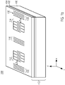
- Figure 1 shows a coupled cavity surface acoustic wave filter structure according to a first embodiment of the invention.
- the coupled cavity surface acoustic wave filter structure 100 is realized on a substrate 102, being a composite substrate.
- the composite substrate 102 comprises a layer of piezoelectric material 104, with crystallographic axis X, Y and Z, formed over a base substrate 106.
- the piezoelectric layer 104 in this embodiment is LiTaO 3 or LiNbO 3 , particularly with cut orientations defined by (YX I )/ ⁇ according to the standard IEEE 1949 Std-176, with ⁇ , an angle of the crystallographic orientation being comprised between 0° and 60° or between 90° and 150°, Potassium Niobate KNbO 3 and similar material composition such as KTN, as well as other piezoelectric layers using sputtered or epitaxial films, for instance Aluminium Nitride AIN, Zinc Oxide ZnO, PZT, GaN or any composition of AIN and GaN.
- the thickness of the piezoelectric layer 104 formed on the base substrate 106 is of the order of one wavelength ⁇ or smaller, in particular is of about 20 ⁇ m or less.
- the thickness t of the base substrate 106 is larger than the thickness of the piezoelectric layer 104.
- a preferred situation corresponds to a base substrate thickness that is at least ten times larger than the thickness of the piezoelectric layer 104, in particular 50 to 100 times larger, which would correspond to a base substrate thickness equal to 250 - 500 ⁇ m.
- the base substrate 106 used in the first embodiment of the invention is a Silicon substrate, in particular a high resistivity Silicon substrate.
- the orientation of the Silicon substrate is preferably (100) due to the higher acoustic wave propagation velocity compared to other crystalline orientation, such as for example (110), (111) or (001), which can however be used.
- other substrate materials with an acoustic wave propagation velocity larger than the one of the piezoelectric layer can be chosen, such as Carbon-Diamond, Sapphire, or Silicon Carbide can be used.
- the base substrate 106 may further comprise a so called trap-rich layer close to the top layer of piezoelectric material, said trap-rich layer improving the isolation performance of the base substrate and may be formed by at least one of polycrystalline, amorphous, or porous materials such as for instance polycrystalline Silicon, amorphous Silicon, or porous Silicon, but the invention is not limited to such materials.
- the base substrate 106 can further comprise a Bragg mirror, underneath the piezoelectric layer 104.
- the Bragg mirror consists of a stack of layers with periodically alternated acoustic impedance deposited or manufactured on top of a plate of any inorganic material.
- the acoustic impedance is the product of the wave velocity times the material density and is expressed in Rayleigh and preferably in Mrayleigh, i.e. 10 6 Rayleigh.
- a piezoelectric layer is deposited or manufactured atop the layer stack for the excitation and detection of acoustic waves.
- the stack may be advantageously composed of an alternation of Tungsten and Silica, or Si 3 N 4 and SiO 2 , or Mo and Al, and in general any couple of material exhibiting an acoustic impedance ratio larger than two.
- the inorganic sub plate may be advantageously standard silicon or high resistivity silicon or glass and generally any material exhibiting a thermal coefficient of expansion (TCE) smaller than 6ppm/K. It can also incorporate a trap-rich layer to improve electrical isolation.
- the first layer of the stack can be SiO 2 or in general any material that can be used to bound the piezoelectric layer to the above-described composite substrate.
- a thin SiO 2 layer 108 is provided at the interface 110 between the piezoelectric layer 104 and the base substrate 106 to improve the attachment of the piezoelectric material layer 104 to the base substrate 106.
- the SiO 2 layer 110 is 200nm thick, but in a variant, the thickness of the SiO 2 layer 110 can vary and be more or less than 200nm thick, in particular can vary between 10nm and 6 ⁇ m.
- the coupled cavity filter structure 100 comprises also two transducer structures 112, 114 and one reflecting structure 116, positioned between the two transducer structures 112, 114 at a certain distance d of the transducer structures 112, 114 in the direction of propagation X as shown in fig. 1 .
- various acoustic cavities are present in the direction of propagation of the acoustic wave
- two acoustic cavities 120 are present.
- the reflecting structure 116 usually comprises one or more metallic strips 122, and is defined by the pitch (not shown) of the metallic strips 122, corresponding to the distance between the metallic strips 122 within the reflecting structure 116.
- the transducer structure 112 and 114 correspond to an input transducer structure 112 and an output transducer structure 114, but their position can also be exchanged so that the input transducer structure is on the right side and the output transducer structure is on the left side of the structure, in the direction of propagation of the acoustic wave.
- the E sign represents the input acoustic signal while the S sign represents the output acoustic signal of the transducer structures.
- Each transducer structure 112, 114 comprises two inter-digitated comb electrodes 124, 126, each comprising a plurality of electrode means 128, 130 respectively.
- the electrode means 128, 130 have the shape of electrode fingers.
- the comb electrodes 124, 126 and its respective electrode fingers 128, 130 are formed of Aluminium-based material, for example pure Aluminium or Aluminium alloy such Al doped with Cu, Si or Ti. Nevertheless, other material may be used which generates stronger reflection coefficient for smaller electrode relative thickness.
- the preferred electrode materials are Copper (Cu), Molybdenum (Mo), Nickel (Ni), Platinum (Pt) or Gold (Au) with an adhesion layer such as Titanium (Ti) or Tantalum (Ta) or Chromium (Cr), Zirconium (Zr), Palladium (Pd), Iridium (Ir), Tungsten (W), etc.
- the transducer structures 112, 114 are also defined by the electrode pitch p (not shown), corresponding to the edge-to-edge electrode finger distance between two neighbouring electrode fingers 128, 130 from opposite comb electrodes 124 and 126.
- ⁇ the operating acoustic wavelength of said transducer structures 112, 114.
- the inter-digitated transducer can operate out of the Bragg conditions, for instance, using a 3 or 4-finger-per-wavelength excitation structure or 5 -finger-per-two-wavelength transducers or 7 or 8 finger-per-three wavelength.
- the transducer structures 112 and 114 can be symmetrical, namely they have the same number of electrode fingers 128, 130 with the same characteristics. However, in a variant of the invention, they can also be different, in particular they can have a different number of electrode fingers 128, 130.
- the electrode fingers 132, 134 of the comb electrodes 128, 130 all have essentially the same length I , width w as well as thickness h. According to a variant of the embodiment, the electrode fingers 132, 134 can have different length /, width wand thickness h.
- the dimensions are adapted to obtain a desired coupling coefficient k s , or to take advantage of other features such as elimination of transverse modes, modulation of the IDT impedance, reduction of unwanted mode emission, etc.
- the transducer structures 112, 114 may be chirped, which means that the electrode pitch p in the transducer structure may be changed continuously in a linear way or in an hyperbolic way. This will enable to enlarge the operation frequency band of the transducer and may yield some robustness versus temperature.
- the pitch of the metallic strips 122 of the reflecting structure 116 can be the same as the electrode pitch p of the transducer structure 112, 114. In a variant, the pitch of the metallic strips 122 of the reflecting structure 116 can be different to the electrode pitch p of the transducer structure 112, 114.
- the reflecting structure 116 can be chirped as well to increase the operating band of the filter and the efficiency of the resonance of the acoustic cavities 118 located in between the transducer structures 112, 114.
- the coupled cavity filter structure 100 further comprises two Bragg mirrors 132, 134.
- This variant is shown in figure 1b , where each Bragg mirror 132, 134 is positioned next to a transducer structure 112, 114, on the outside of the coupled cavity filter structure 200, meaning on the other side where the reflecting structure 116 is located, in the direction of propagation of the acoustic wave.
- Each Bragg mirror 132, 134 is positioned at a distance s of its respective transducer structure 112, 114.
- Each Bragg mirror 132, 134 comprises one or more metallic strips 136 and is defined by the pitch (not shown) of the metallic strips 136, corresponding to the distance between the metallic strips 136 within the Bragg mirror 132, 134.
- the reflecting structure 116 and the Bragg mirrors 132, 134 can be built by etching grooves instead of depositing metallic strips 136, 210.
- the grooves may be etched in the piezoelectric layer 104 of the composite substrate 102 and even down to the base substrate 106.
- a passivation layer (not shown) can be formed over the transducer structures 112, 114 and the at least one reflecting structure 116.
- the passivation layer has a predetermined thickness which is the same or different over the transducer structures 112, 114 and/or the at least one reflecting structures 116.
- the passivation layer can also be formed over the Bragg mirrors 132, 134.
- the substrate may be a monolithic piezoelectric wafer such as Lithium Tantalate or Lithium Niobate bulk wafers and the passivation layer could be advantgeously a Silica SiO 2 layer or a Tantalum Pentoxide Ta 2 O 5 layer.
- the passivation layer has a positive thermal coefficient of expansion (TCE) whereas the substrate has a negative thermal coefficient of expansion (TCE), the layer thickness being set to reduce the temperature coefficient of frequency (TCF) of the SAW device.
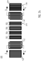
- Figures 2a to 2e show the coupled cavity filter structure according to a second embodiment of the invention and its variants.
- the coupled cavity filter structure is shown in a 2D plan view and the substrate on which it is positioned is not shown anymore.
- the substrate is the same as the substrate 102 of fig. 1a , 1b .
- the same reference numbers as in fig. 1a and 1b will be used to refer to the same features and will not be explained again in details.
- the coupled cavity filter structure 300 comprises like the coupled cavity filter structure 200, two transducer structures 112, 114 with two Bragg mirrors 132, 134 each positioned next to one transducer structure.
- the difference with the coupled cavity filter 200 is that a plurality of reflecting structures , namely four reflecting structures 202, 204, 206, 208, are present in between the transducer structures 112, 114.
- Each reflecting structure 202, 204, 206, 208 of the plurality of reflecting structure comprises at least one or more metallic strips 210 and are defined by the pitch (not shown) of the metallic strips 210, corresponding to the distance between the metallic strips 210 within each reflecting structure 202, 204, 206, 208.
- each reflecting structure 204, 206, 208, 210 amount to four, but it can be more or less.
- the reflecting structures 204, 206, 208, 210 of the plurality of reflecting structures can also have the same number of metallic strips 210 but in a variant, they can each have different number of metallic strips 210.
- the number of metallic strips 210 in the reflecting structures 204, 206, 208, 210 can increase then decrease throughout the whole reflecting structures 204, 206, 208, 210 in between the transducer structures 112, 114 to reinforce the resonance at the actual center of the structure.
- These reflecting structures 202, 204, 206, 208 are separated from each other by a gap g.
- the region located between a reflecting structure and an adjacent transducer structure corresponds also to an acoustic cavity 214, but with a width defined by the distance d between the reflective structure and the adjacent transducer structure.
- the coupled cavity surface acoustic wave filter structure various cavities are present in the direction of propagation of the acoustic wave, being separated by a reflecting structure, or said otherwise, a cavity is surrounded by two reflecting structures in between the transducer
- a total of five acoustic cavities 212, 214 are present, in the direction of propagation of the mode.
- the number of acoustic cavities equal the number of reflecting structure plus one.
- the reflecting structures 202, 204, 206, 208 can be chirped as well to increase the operating band of the filter and the efficiency of the resonance of the acoustic cavities 212, 214 located in between the transducer structures 212, 214.
- the reflecting structures 202, 204, 206, 208 and the Bragg mirrors 132, 134 can be built by etching grooves instead of depositing metallic strips 136, 210.
- the grooves may be etched in the piezoelectric layer 104 of the composite substrate 102 and even down to the base substrate 106.
- the metallic strips 136, 210 of the reflecting structures 202, 204, 206, 208 and / or of the Bragg mirrors 132, 134 can be electrically connected to each other.
- the variant where the reflecting strips 136, 210 of both the reflecting structures 202, 204, 206, 208 and the Bragg mirrors 132, 134 are connected to each other is shown in fig. 2b for the coupled cavity filter structure 400. This results in an improvement of the reflection coefficient of the reflecting structures 202, 204, 206, 208 and of the Bragg mirrors 132, 134 at the Bragg condition.
- All the reflecting structures 202, 204, 206, 208 and / or Bragg mirrors 132, 134 are operating in the so-called short-circuit conditions, meaning that all the metallic strips 136, 210 of a given reflecting structure 202, 204, 206, 208 / Bragg mirror 132, 134 are connected to one another, yielding a constant value of the electrical potential throughout the said grating structure.
- the coupled cavity filter structure can comprise three transducer structures or even more.
- fig. 2c is shown the variant where three transducers structures 402, 404, 406 are present in the coupled cavity filter structure 400.
- the coupled cavity filter structure 400 is also different from the coupled cavity filter structure 300 as shown in fig. 2a as the plurality of reflecting structures comprises in total six reflecting structures 302, 304, 306, 308, 310, 312. Again, the same reference numbers will be used to describe the same features already described in fig. 2a for the coupled cavity filter structure 300.
- Two of the transducer structures 112, 114 are positioned, like in the structure of fig. 2a , on the outside of the reflecting structures 302, 304, 306, 308, 310, 312 while the third transducer structure 314 is positioned in the middle of the reflecting structures 302, 304, 306, 308, 310, 312116, so that on each side of the third transducer structure 314, three reflecting structures 302, 304, 306 and 308, 310, 312 are present.
- the transducer structure 314 is also separated from the two adjacent reflecting structure by a distance d, corresponding to the same distance between the transducer structure 112, 114 and their respective neighbouring reflecting structure, here 302 for the transducer structure 112 and 312 for the transducer structure 114.
- the coupled cavity filter 500 comprises then in total eight acoustic cavities 316.
- Such a cavity filter structure 500 is symmetrical and results in a stronger confinement of energy in the cavities 316 compare to the cavity filter structure 300 as shown in fig. 2a , with only two transducer structures 112, 114.
- the third transducer 314 is not positioned in the middle of the coupled cavity filter structure so that the coupled cavity filter structure is not symmetrical.
- the plurality of acoustic cavities can be split into sub-cavities.
- This variant is shown in fig. 2d , where the sub-cavities are separated from one another by the presence of additional layers.
- the coupled cavity filter structure 600 is also different from the coupled cavity filter structure 300 as shown in fig. 2a as the plurality of reflecting structures comprises in total three reflecting structures 402, 404, 406. Again, the same reference numbers will be used to describe the same features already described in fig. 2a for the coupled cavity filter structure 300.
- the acoustic cavities 408 located in between the reflecting structures 402, 404, 406 and between a transducer structure 112, 114 and its neighbouring reflecting structure 402 and 406 respectively, are split in two sections, resulting in the presence of eight dark regions 410 and four white regions 412 between the two transducer structures 112, 114.
- the dark regions 410 represent locations where the wave velocity is smaller than in the white regions 412, thus leading to a better energy confinement than in the coupled cavity filter structure 300 shown in fig. 2a .
- the coupled cavity filter structure 600 yields additional poles, leading to an improvement of the compactness of the coupled cavity filter structure 600.
- the input and output transducer structures are not symmetrical or identical, and this variant is shown in fig. 2e .
- the coupled cavity filter structure 700 is also different from the coupled cavity filter structure 300 as shown in fig. 2a , as the plurality of reflecting structures comprises in total two reflecting structures 502, 504.
- the same reference numbers will be used to describe the same features already described in fig. 2a for the coupled cavity filter structure 300.
- the number of electrode fingers of each transducer structure is different.
- the transducer structure 114 comprises inter-digitated comb electrodes 124, 126 with each five electrode fingers 128, 130, with a constant electrode pitch p throughout the whole transducer structure 114.
- the transducer structure 506 comprises inter-digitated comb electrodes 508, 510, but they each have eight electrode fingers 128, 130 and furthermore a gap is present in the transducer structure 506 between the third electrode finger 128 of the comb electrode 508 and the fourth electrode finger 130 of the comb electrode 510. Furthermore, in this variant, no Bragg mirrors are present next to the transducer structures 114, 506, which will yield more losses and ripples than the coupled cavity filter structure 300 of fig. 2a . However, this coupled cavity filter structure 700 offers a more compact and simpler design than the structure shown in fig. 2a .
- the coupled cavity surface acoustic wave filter structure functions in the following way.
- An input inter-digitated transducer (IDT) emits acoustic energy toward the reflecting structure and excites its resonance.
- the reflecting structure is coupled to another one which therefore generates coupling conditions yielding energy transfer from one reflecting structure to another.
- a plurality of such reflecting structures can be coupled to one another but there is at least one output transducer structure which collects the transmitted energy.
- the invention proposes to use a coupled cavity filter structure which takes advantage of the wave guidance of the top piezoelectric layer from the composite substrate and uses acoustic resonant cavities that couple energy from one reflecting structure to another.
- the relation of the reflection coefficient with respect to the coupling coefficient can be achieved with the composite substrate, even when the coupling coefficient of the transducer structure is 5% or more. This is particularly true, when using shear waves or longitudinally waves guided in the piezoelectric layer of the composite substrate.
- the thickness of the piezoelectric layer being lower than the wavelength, a shear wave mode or a longitudinal mode is guided within the piezoelectric layer. Furthermore, the energy loss in the composite substrate can be reduced.
- the thickness of the piezoelectric layer should be larger than or equal to 5% of the wavelength ⁇ .
- the shear mode of a composite substrate is not entirely guided anymore but has a lossy bulk component which reflects at the interface to the base substrate and leads to parasitic modes or rattle effect. These effects typically occur when at least two modes are excited.
- a thin piezoelectric layer typically corresponds to a thickness up to 50% of the wavelength ⁇ and a thick piezoelectric layer to a layer of more than 50% of the wavelength ⁇ .
- the fundamental mode can typically be exploited up to a thickness of 1.5 times ⁇ .
- the figure of merit of a filter device is the transmission of the filter which shows the filter bandpass as a function of the frequency with the level of losses in dB in the bandpass.
- the filter bandpass depends on various factors, namely the coupling coefficient, the number of cavities and the coefficient of reflection.
- said acoustic cavities should ideally be a quarter wavelength long or an odd number of quarter wavelength to meet the optimal resonance conditions according to the state of the art.
- the acoustic cavities length can be inferior to a quarter wavelength. This is due to the strong velocity change from free surface to grating area, yielding an acoustic impedance mismatch much larger than accessible using standard true SAW solutions
- the coupling coefficient is directly related to the bandpass value by a factor 0.7, so that the required bandpass of the filter device can be obtained by choosing the materials and the dimensions of the cavity filter structure.
- the magnitude of the reflection coefficient preferably is larger than the coupling coefficient, ideally 1.5 times higher or more than the coupling coefficient parameter.
- a reflection coefficient larger than 15% allows for reducing the number of metallic strips composing the reflecting structures, which directly impacts the bandwidth of the filter: the smaller the number of metallic strips in the reflecting structures, the larger the bandwidth, provided the reflection coefficient of the structure is large or equal 50%. Considering a reflection coefficient larger than 15%, a filter with bandwidth larger than 5% can be achieved.
- a particular example of a filter device operating at 2.6GHz with a bandwidth in excess of 7% and in-band ripples smaller than 0.6dB is given with a 30nm thick Tantalum (Ta) electrodes on a composite substrate comprising a 300nm thick (YX/)/52° LiNbO 3 layer on a 1 ⁇ m thick SiO 2 layer onto (100) Silicon substrate.
- Ta Tantalum
- the reflection coefficient reaches 20% and the coupling factor about 18%.
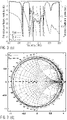
- Figures 3a - 3d show the characteristics of a surface acoustic wave filter device comprising a cavity filter structure as shown in fig. 2b , with a composite substrate according to the invention, with a SiO 2 layer of 500nm in between a LiTaO 3 (YX/)/42° piezoelectric layer of 6 ⁇ m and a semi-infinite (100) Silicon substrate.
- This configuration is suitable to operate in the frequency range 50 to 250MHz.
- the coupled cavity filter structure shown in fig. 2b was used, namely an input and an output transducer structures with each an adjacent Bragg mirror, four reflecting structures leading to five acoustic cavities present in between the transducer structures.
- the inter-digitated transducer structure have an electrode pitch set to 9.95 ⁇ m and a ratio a/p set to 0.3, with a number of electrode finger pair set to 15. Furthermore, the mirror grating period is set to 10 ⁇ m and a/p to 0.4, with 30 electrodes.
- the gap between the mirror grating and the inter-digitated transducer structure is set to 9 ⁇ m, corresponding to about half a wavelength.
- Two internal reflecting structures of 14 electrodes each are separated by a gap g of 4.8 ⁇ m, corresponding to about a quarter wavelength. The aperture is then 3.1mm.
- Figure 3a shows a general view of the filter transfer function and the group delay of the filter as a function of frequency (MHz), from 170 to 250MHz.
- the group delay is a measure of the phase linearity.
- Figure 3b shows a zoom of fig. 3a near the central frequency and thus focuses on the bandpass, showing the very low losses of the transfer.
- Figure 3c is the reflection coefficient, showing the signature of the pole of the filter (minimum
- Figure 3d is a Smith abacus plot of the so-called reflection coefficient currently used by the skilled person in the art to assess electrical impedance matching of both ports of the filter. The reflection coefficient must be centered around the 50 Ohm condition, i.e. the center of the abacus to be matched.
- the transfer function in fig. 3a indicates the performance of the device, with a filter bandpass between 210 and 218MHz.
- fig. 3b it can be seen that the filter bandpass shows a flat profile at around 0.5dB with low in-band ripples.
- Figure 4 shows a table listing the characteristics of the coupled cavity surface acoustic wave filter structure as shown in fig. 2b , according to the invention.
- the composite substrate used was the same as for fig. 3 , namely a LiTaO 3 (YX/)/42° piezoelectric layer of 6 ⁇ m, with a SiO 2 layer of 500nm in between the piezoelectric layer and the semi-infinite (100) Silicon base substrate.
- the coupled cavity filter structure corresponds to fig. 2b , namely an input and an output transducer structures with each an adjacent Bragg mirror, four reflecting structures leading to five acoustic cavities present in between the transducer structures.
- the metallic strips of both each reflecting structures and the Bragg mirrors are connected to each other for a short-circuit operation.
- All the coupled cavity filter structures described in figure 4 correspond to the propagation of a pure shear wave mode and show performance, i.e. a filter band-pass varying from 0,5 to 10%, low insertion loss of below 2dB, with a 15dB to 20dB rejection loss, a coupling factor above 5% and temperature coefficient of frequency (TCF) below 20ppm/K.
- Bandpass as large as 10% can be achieved using LNO thin layers with for instance Pt or W or Ta or Mo based electrodes with thickness compatible with current deposition technologies, namely with h/A equal of less than 5%, with h the absolute thickness of the metal strip).
- a coupled cavity SAW filter device uses a shear wave of a composite substrate in order to obtain a narrow filter band-pass comprised between 0.5% and 10%, low insertion loss of below 2dB, with a 15dB to 20dB rejection loss as well as low ripples within the filter band-pass, with a reduced size due to an improved compactness.
Landscapes
- Physics & Mathematics (AREA)
- Acoustics & Sound (AREA)
- Surface Acoustic Wave Elements And Circuit Networks Thereof (AREA)
Claims (25)
- Structure de filtre à cavités couplées utilisant une onde acoustique de surface guidée comprenant :un substrat de propagation d'onde acoustique (102) ;au moins une structure de transducteur d'entrée (112, 506) et une structure de transducteur de sortie (114, 506), disposées sur le substrat (102), chacune comprenant des électrodes en peigne imbriquées (124, 126, 508, 510),une structure de réflexion (116), ladite structure de réflexion (116) comprenant au moins une ou plusieurs bandes métalliques (122), positionnées entre les structures de transducteur d'entrée et de sortie (112, 114, 506) à une distance d des structures de transducteur d'entrée et de sortie (112, 114, 506), dans la direction de propagation d'une onde acoustique,caractérisée en ce quele substrat de propagation d'onde acoustique (102) est un substrat composite comprenant un substrat de base (106) et une couche piézoélectrique (104), dans laquelle l'épaisseur de la couche piézoélectrique (104) est inférieure ou égale à 1,5 λ, dans laquelle λ est la longueur d'onde du mode fondamental de l'onde acoustique de surface guidée, et chaque zone (118) située entre ladite structure de réflexion (116) et chacune de la structure de transducteur d'entrée (112, 114, 506) et la structure de transducteur de sortie (112, 114, 506) respectivement, forme une cavité acoustique (120) avec sa largeur définie par la distance d,et le filtre de cavité couplé est configuré de sorte que l'onde acoustique de surface guidée est une onde de cisaillement guidée ou une onde longitudinale guidée à l'intérieur de la couche piézoélectrique (104).
- La structure de filtre à cavités couplées selon la revendication 1, dans laquelle les électrodes en peigne imbriquées (124, 126) de l'au moins une structure de transducteur d'entrée (112) et une structure de transducteur de sortie (114) sont définies par la condition de Bragg donnée par p = λ/2, λ étant la longueur d'onde acoustique de fonctionnement desdites structures de transducteur (112, 114) et p étant le pas d'électrode desdites structures de transducteur (112, 114) .
- Structure de filtre à cavités couplées selon l'une des revendications 1 à 2, comprenant en outre au moins un miroir de Bragg (132, 134), installé à part de la structure de transducteur d'entrée et/ou de sortie (112, 114) sur le côté opposé du côté où l'une structure de réflexion (116) est installée, dans la direction de propagation de l'onde acoustique.
- La structure de filtre à cavités couplées selon l'une des revendications 1 à 3, comprenant une pluralité de structures de réflexion séparées l'une de l'autre par un écart g et positionnées entre les structures de transducteur d'entrée et sortie (112, 114, 506) à une distance d de la structure de transducteur d'entrée et de sortie (112, 114, 506), dans la direction de propagation d'une onde acoustique, chaque écart g entre les structures de réflexion (116, 202, 204, 206, 208, 302, 304, 306, 308, 310, 312, 402, 404, 406 ) et chaque distance d entre une structure de transducteur (112, 114) et sa structure de réflexion voisine constituant une cavité acoustique (120, 212, 214, 316, 408).
- La structure de filtre à cavités couplées selon l'une des revendications 1 à 4, dans laquelle la dimension de chaque cavité acoustique (120, 212, 214, 316, 408) est inférieure à λ/4.
- La structure de filtre à cavités acoustiques selon l'une des revendications 1 à 5, dans laquelle la dimension de chaque cavité acoustique (120, 212, 214, 316, 408) est telle que la vélocité de phase dans la cavité acoustique (120, 212, 214, 316, 408) est supérieure à la vélocité de phase au sein de la structure de réflexion (116, 202, 204, 206, 208, 302, 304, 306, 308, 310, 312, 402, 404, 406).
- La structure de filtre à cavités couplées selon l'une des revendications 4 à 6, dans laquelle les écarts g entre des structures de réflexion voisines (202, 204, 206, 208, 302, 304, 306, 308, 310, 312, 402, 404, 406) de la pluralité de structures de réflexion et/ou la distance d entre une structure de réflexion (116, 202, 204, 206, 208, 302, 304, 306, 308, 310, 312, 402, 404, 406) et une structure de transducteur voisine (112, 114, 506) sont identiques.
- La structure de filtre à cavités couplées selon l'une des revendications 4 à 6, dans laquelle les écarts g entre des structures de réflexion voisines (202, 204, 206, 208, 302, 304, 306, 308, 310, 312, 402, 404, 406) de la pluralité de structures de réflexion et/ou la distance d entre une structure de réflexion (116, 202, 204, 206, 208, 302, 304, 306, 308, 310, 312, 402, 404, 406) et une structure de transducteur voisine (112, 114, 506) sont différents.
- La structure de filtre à cavités couplées selon l'une des revendications 1 à 8, dans laquelle la structure de réflexion (116) ou les structures de réflexion (202, 204, 206, 208, 302, 304, 306, 308, 310, 312, 402, 404, 406) présente/présentent un coefficient de réflexion relatif à une bande métallique unitaire supérieur au coefficient de couplage ks 2 relative au substrat composite (102) et aux électrodes en peigne (124, 126, 604, 606) de la structure de transducteur (112, 114, 506) .
- La structure de filtre à cavités couplées selon l'une des revendications 1 à 9, dans laquelle les structures de transducteur d'entrée et de sortie (112, 114, 506) présentent un nombre différent de tiges d'électrode (128, 130).
- La structure de filtre à cavités couplées selon l'une des revendications 1 à 10, dans laquelle chaque structure de réflexion (116, 202, 204, 206, 208, 302, 304, 306, 308, 310, 312, 402, 404, 406) de la pluralité de structures de réflexion comprend des bandes métalliques (122, 210) avec un pas des bandes métalliques identique au pas d'électrode p des structures de transducteur d'entrée et de sortie (112, 114, 506) .
- La structure de filtre à cavités couplées selon l'une des revendications 1 à 10, dans laquelle chaque structure de réflexion (116, 202, 204, 206, 208, 302, 304, 306, 308, 310, 312, 402, 404, 406) de la pluralité de structures de réflexion comprend des bandes métalliques (122, 210) avec un pas des bandes métalliques différent du pas d'électrode p des structures de transducteur d'entrée et de sortie (112, 114, 506) .
- La structure de filtre à cavités couplées selon l'une des revendications 1 à 12, dans laquelle les bandes métalliques (124) de chaque structure de réflexion (116, 202, 204, 206, 208, 302, 304, 306, 308, 310, 312, 402, 404, 406) de la pluralité de structures de réflexion sont électriquement connectées l'une à l'autre.
- La structure de filtre à cavités couplées selon l'une des revendications 1 à 13, dans laquelle le nombre de bandes métalliques (122, 210) de chaque structure de réflexion (116, 202, 204, 206, 208, 302, 304, 306, 308, 310, 312, 402, 404, 406) de la pluralité de structures de réflexion est inférieur à 30, de sorte que le coefficient de réflexion de la pluralité de structures de réflexion est supérieur à 0,5.
- La structure de filtre à cavités couplées selon l'une des revendications 1 à 14, dans laquelle la différence entre l'impédance acoustique du matériau de la couche piézoélectrique (104) et du matériau des bandes métalliques (122, 210) de la pluralité de structures de réflexion est telle que le coefficient de réflexion de la pluralité de structures de réflexion est supérieur à 0,5.
- La structure de filtre à cavités couplées selon l'une des revendications 1 à 15, dans laquelle les cavités acoustiques (120, 212, 214, 316, 408) sont divisées en sous-cavités (410) séparées l'une de l'autre.
- La structure de filtre à cavités couplées selon l'une des revendications 1 à 16, comprenant au moins trois structures de transducteur (112, 114, 314, 506) ou plus dans la direction de propagation de l'onde acoustique.
- La structure de filtre à cavités couplées selon l'une des revendications 1 à 17, dans laquelle les caractéristiques de la couche piézoélectrique (104) et des électrodes (124, 126, 508, 510) des structures de transducteur (112, 114, 314, 506) sont choisies de sorte que le coefficient de couplage électromagnétique ks 2 de l'onde de cisaillement guidée, ou de l'onde longitudinale guidée, dans la couche piézoélectrique (104) est supérieur à 5 %.
- La structure de filtre à cavités couplées selon l'une des revendications 1 à 18, dans laquelle l'épaisseur de la couche piézoélectrique (104) est choisie de sorte que le coefficient de couplage électromagnétique ks 2 de l'onde de cisaillement guidée, ou de l'onde longitudinale guidée, dans la couche piézoélectrique (104) est supérieur à 5 %.
- La structure de filtre à cavités couplées selon l'une des revendications 1 à 19, comprenant en outre une couche diélectrique (108), intercalée entre le substrat de base (106) et la couche piézoélectrique (104).
- La structure de filtre à cavités couplées selon l'une des revendications 1 à 20, dans laquelle la couche piézoélectrique (104) est en nitrure d'aluminium (AlN), oxyde de zinc (ZnO), PZT, nitrure de gallium (GaN), tantalate de lithium LiTa03 ou niobate de lithium LiNb03 avec une orientation cristallographique pour le tantalate de lithium LiTa03 ou le niobate de lithium LiNb03 définie comme (YX/)/θ selon la norme IEEE 1949 Std-176, avec θ, un angle de l'orientation cristallographique compris entre 0 ° et 60 ° ou entre 90 ° et 150 °.
- La structure de filtre à cavités couplées selon l'une des revendications 1 à 21, dans laquelle le substrat de base (106) du substrat composite (102) est un de silicium, de carbone diamant, de saphir, de quartz ou de carbure de silicium.
- La structure de filtre à cavités couplées selon l'une des revendications 1 à 22, dans laquelle le substrat de base (106) comprend un miroir de Bragg sous la couche piézoélectrique (104).
- La structure de filtre à cavités couplées selon l'une des revendications 1 à 23, dans laquelle le filtre passe-bande est compris entre 0,5 % et 10 %.
- La structure de filtre à cavités couplées selon l'une des revendications 1 à 24 comprenant en outre une couche de passivation formée par-dessus des structures de transducteur (112, 114, 314, 506) et l'au moins une structure de réflexion, la couche de passivation présentant une épaisseur prédéterminée qui est identique ou différente par-dessus des structures de transducteur (112, 114, 314, 506) et/ou l'au moins une structure de réflexion.
Priority Applications (13)
| Application Number | Priority Date | Filing Date | Title |
|---|---|---|---|
| EP18306023.5A EP3599720B1 (fr) | 2018-07-27 | 2018-07-27 | Filtres utilisant des resonateurs couples à ondes acoustiques de surface |
| TW108126427A TWI734153B (zh) | 2018-07-27 | 2019-07-25 | 共振腔表面聲波(saw)濾波器 |
| PCT/EP2019/070082 WO2020021029A2 (fr) | 2018-07-27 | 2019-07-25 | Filtres à ondes acoustiques de surface (saw) à cavité résonante |
| CA3106887A CA3106887A1 (fr) | 2018-07-27 | 2019-07-25 | Filtres a ondes acoustiques de surface (saw) a cavite resonante |
| US17/263,880 US11848663B2 (en) | 2018-07-27 | 2019-07-25 | Resonant cavity surface acoustic wave (SAW) filters |
| JP2021503896A JP7408896B2 (ja) | 2018-07-27 | 2019-07-25 | 共振キャビティ表面音響波(saw)フィルタ |
| EP19742238.9A EP3830956A2 (fr) | 2018-07-27 | 2019-07-25 | Filtres à ondes acoustiques de surface (saw) à cavité résonante |
| CN201980050135.XA CN112840561A (zh) | 2018-07-27 | 2019-07-25 | 谐振腔表面声波(saw)滤波器 |
| KR1020217006224A KR102671258B1 (ko) | 2018-07-27 | 2019-07-25 | 공동 공진 saw 필터 |
| KR1020247009398A KR20240044522A (ko) | 2018-07-27 | 2019-07-25 | 공동 공진 saw 필터 |
| JP2023035978A JP2023076477A (ja) | 2018-07-27 | 2023-03-08 | 共振キャビティ表面音響波(saw)フィルタ |
| US18/504,791 US12095449B2 (en) | 2018-07-27 | 2023-11-08 | Resonant cavity surface acoustic wave (SAW) filters |
| US18/754,943 US20240348234A1 (en) | 2018-07-27 | 2024-06-26 | Resonant cavity surface acoustic wave (saw) filters |
Applications Claiming Priority (1)
| Application Number | Priority Date | Filing Date | Title |
|---|---|---|---|
| EP18306023.5A EP3599720B1 (fr) | 2018-07-27 | 2018-07-27 | Filtres utilisant des resonateurs couples à ondes acoustiques de surface |
Publications (2)
| Publication Number | Publication Date |
|---|---|
| EP3599720A1 EP3599720A1 (fr) | 2020-01-29 |
| EP3599720B1 true EP3599720B1 (fr) | 2022-06-29 |
Family
ID=63209342
Family Applications (1)
| Application Number | Title | Priority Date | Filing Date |
|---|---|---|---|
| EP18306023.5A Active EP3599720B1 (fr) | 2018-07-27 | 2018-07-27 | Filtres utilisant des resonateurs couples à ondes acoustiques de surface |
Country Status (1)
| Country | Link |
|---|---|
| EP (1) | EP3599720B1 (fr) |
Families Citing this family (4)
| Publication number | Priority date | Publication date | Assignee | Title |
|---|---|---|---|---|
| EP3830956A2 (fr) * | 2018-07-27 | 2021-06-09 | Frec|N|Sys | Filtres à ondes acoustiques de surface (saw) à cavité résonante |
| FR3114875B1 (fr) * | 2020-10-01 | 2023-01-20 | Frecnsys | Dispositif à résonateurs |
| WO2022140653A1 (fr) * | 2020-12-23 | 2022-06-30 | Murata Manufacturing Co., Ltd. | Dispositif à ondes acoustiques |
| FR3127660A1 (fr) | 2021-09-27 | 2023-03-31 | Frec'n'sys | Filtre a ondes elastiques de surface et a cavites resonantes |
Family Cites Families (5)
| Publication number | Priority date | Publication date | Assignee | Title |
|---|---|---|---|---|
| DE2363701A1 (de) * | 1973-12-21 | 1975-06-26 | Licentia Gmbh | Akustisches oberflaechenwellenfilter |
| US3970970A (en) * | 1975-06-30 | 1976-07-20 | Motorola, Inc. | Multiple acoustically coupled surface acoustic wave resonators |
| US7569971B2 (en) * | 2007-10-02 | 2009-08-04 | Delaware Capital Formation, Inc. | Compensation of resonators for substrate and transducer asymmetry |
| CN105723615B (zh) * | 2013-11-29 | 2018-07-27 | 株式会社村田制作所 | 分波器 |
| CN108028637B (zh) * | 2015-10-23 | 2021-05-11 | 株式会社村田制作所 | 弹性波装置 |
-
2018
- 2018-07-27 EP EP18306023.5A patent/EP3599720B1/fr active Active
Also Published As
| Publication number | Publication date |
|---|---|
| EP3599720A1 (fr) | 2020-01-29 |
Similar Documents
| Publication | Publication Date | Title |
|---|---|---|
| US12095449B2 (en) | Resonant cavity surface acoustic wave (SAW) filters | |
| TWI762832B (zh) | 聲表面波器件 | |
| US7659653B2 (en) | Acoustic wave device and filter | |
| EP3599720B1 (fr) | Filtres utilisant des resonateurs couples à ondes acoustiques de surface | |
| EP3776854A1 (fr) | Dispositif à ondes acoustiques de surface sur substrat composite | |
| US10886893B2 (en) | Reduced-size guided-surface acoustic wave (SAW) devices | |
| US20240186986A1 (en) | Surface elastic wave filter with resonant cavities | |
| US6940208B2 (en) | Surface acoustic wave device | |
| JPH0865088A (ja) | 表面弾性波素子 | |
| US20230412142A1 (en) | Piezoelectric layer arrangements in acoustic wave devices and related methods | |
| EP3796555A1 (fr) | Structure de transducteur pour dispositif d'onde acoustique | |
| EP3796556A1 (fr) | Structure de transducteur pour dispositif d'onde acoustique | |
| CN118487570A (zh) | 一种声表面波谐振器及其机电耦合系数的调节方法 |
Legal Events
| Date | Code | Title | Description |
|---|---|---|---|
| PUAI | Public reference made under article 153(3) epc to a published international application that has entered the european phase |
Free format text: ORIGINAL CODE: 0009012 |
|
| STAA | Information on the status of an ep patent application or granted ep patent |
Free format text: STATUS: THE APPLICATION HAS BEEN PUBLISHED |
|
| AK | Designated contracting states |
Kind code of ref document: A1 Designated state(s): AL AT BE BG CH CY CZ DE DK EE ES FI FR GB GR HR HU IE IS IT LI LT LU LV MC MK MT NL NO PL PT RO RS SE SI SK SM TR |
|
| AX | Request for extension of the european patent |
Extension state: BA ME |
|
| STAA | Information on the status of an ep patent application or granted ep patent |
Free format text: STATUS: REQUEST FOR EXAMINATION WAS MADE |
|
| 17P | Request for examination filed |
Effective date: 20200728 |
|
| RBV | Designated contracting states (corrected) |
Designated state(s): AL AT BE BG CH CY CZ DE DK EE ES FI FR GB GR HR HU IE IS IT LI LT LU LV MC MK MT NL NO PL PT RO RS SE SI SK SM TR |
|
| STAA | Information on the status of an ep patent application or granted ep patent |
Free format text: STATUS: EXAMINATION IS IN PROGRESS |
|
| 17Q | First examination report despatched |
Effective date: 20210713 |
|
| STAA | Information on the status of an ep patent application or granted ep patent |
Free format text: STATUS: EXAMINATION IS IN PROGRESS |
|
| GRAP | Despatch of communication of intention to grant a patent |
Free format text: ORIGINAL CODE: EPIDOSNIGR1 |
|
| STAA | Information on the status of an ep patent application or granted ep patent |
Free format text: STATUS: GRANT OF PATENT IS INTENDED |
|
| INTG | Intention to grant announced |
Effective date: 20220121 |
|
| RAP3 | Party data changed (applicant data changed or rights of an application transferred) |
Owner name: FREC'N'SYS |
|
| GRAS | Grant fee paid |
Free format text: ORIGINAL CODE: EPIDOSNIGR3 |
|
| GRAA | (expected) grant |
Free format text: ORIGINAL CODE: 0009210 |
|
| STAA | Information on the status of an ep patent application or granted ep patent |
Free format text: STATUS: THE PATENT HAS BEEN GRANTED |
|
| AK | Designated contracting states |
Kind code of ref document: B1 Designated state(s): AL AT BE BG CH CY CZ DE DK EE ES FI FR GB GR HR HU IE IS IT LI LT LU LV MC MK MT NL NO PL PT RO RS SE SI SK SM TR |
|
| REG | Reference to a national code |
Ref country code: CH Ref legal event code: EP |
|
| REG | Reference to a national code |
Ref country code: DE Ref legal event code: R096 Ref document number: 602018037266 Country of ref document: DE |
|
| REG | Reference to a national code |
Ref country code: AT Ref legal event code: REF Ref document number: 1501999 Country of ref document: AT Kind code of ref document: T Effective date: 20220715 |
|
| REG | Reference to a national code |
Ref country code: IE Ref legal event code: FG4D |
|
| REG | Reference to a national code |
Ref country code: LT Ref legal event code: MG9D |
|
| PG25 | Lapsed in a contracting state [announced via postgrant information from national office to epo] |
Ref country code: SE Free format text: LAPSE BECAUSE OF FAILURE TO SUBMIT A TRANSLATION OF THE DESCRIPTION OR TO PAY THE FEE WITHIN THE PRESCRIBED TIME-LIMIT Effective date: 20220629 Ref country code: NO Free format text: LAPSE BECAUSE OF FAILURE TO SUBMIT A TRANSLATION OF THE DESCRIPTION OR TO PAY THE FEE WITHIN THE PRESCRIBED TIME-LIMIT Effective date: 20220929 Ref country code: LT Free format text: LAPSE BECAUSE OF FAILURE TO SUBMIT A TRANSLATION OF THE DESCRIPTION OR TO PAY THE FEE WITHIN THE PRESCRIBED TIME-LIMIT Effective date: 20220629 Ref country code: HR Free format text: LAPSE BECAUSE OF FAILURE TO SUBMIT A TRANSLATION OF THE DESCRIPTION OR TO PAY THE FEE WITHIN THE PRESCRIBED TIME-LIMIT Effective date: 20220629 Ref country code: GR Free format text: LAPSE BECAUSE OF FAILURE TO SUBMIT A TRANSLATION OF THE DESCRIPTION OR TO PAY THE FEE WITHIN THE PRESCRIBED TIME-LIMIT Effective date: 20220930 Ref country code: FI Free format text: LAPSE BECAUSE OF FAILURE TO SUBMIT A TRANSLATION OF THE DESCRIPTION OR TO PAY THE FEE WITHIN THE PRESCRIBED TIME-LIMIT Effective date: 20220629 Ref country code: BG Free format text: LAPSE BECAUSE OF FAILURE TO SUBMIT A TRANSLATION OF THE DESCRIPTION OR TO PAY THE FEE WITHIN THE PRESCRIBED TIME-LIMIT Effective date: 20220929 |
|
| REG | Reference to a national code |
Ref country code: NL Ref legal event code: MP Effective date: 20220629 |
|
| REG | Reference to a national code |
Ref country code: AT Ref legal event code: MK05 Ref document number: 1501999 Country of ref document: AT Kind code of ref document: T Effective date: 20220629 |
|
| PG25 | Lapsed in a contracting state [announced via postgrant information from national office to epo] |
Ref country code: RS Free format text: LAPSE BECAUSE OF FAILURE TO SUBMIT A TRANSLATION OF THE DESCRIPTION OR TO PAY THE FEE WITHIN THE PRESCRIBED TIME-LIMIT Effective date: 20220629 Ref country code: LV Free format text: LAPSE BECAUSE OF FAILURE TO SUBMIT A TRANSLATION OF THE DESCRIPTION OR TO PAY THE FEE WITHIN THE PRESCRIBED TIME-LIMIT Effective date: 20220629 |
|
| PG25 | Lapsed in a contracting state [announced via postgrant information from national office to epo] |
Ref country code: NL Free format text: LAPSE BECAUSE OF FAILURE TO SUBMIT A TRANSLATION OF THE DESCRIPTION OR TO PAY THE FEE WITHIN THE PRESCRIBED TIME-LIMIT Effective date: 20220629 |
|
| PG25 | Lapsed in a contracting state [announced via postgrant information from national office to epo] |
Ref country code: SM Free format text: LAPSE BECAUSE OF FAILURE TO SUBMIT A TRANSLATION OF THE DESCRIPTION OR TO PAY THE FEE WITHIN THE PRESCRIBED TIME-LIMIT Effective date: 20220629 Ref country code: SK Free format text: LAPSE BECAUSE OF FAILURE TO SUBMIT A TRANSLATION OF THE DESCRIPTION OR TO PAY THE FEE WITHIN THE PRESCRIBED TIME-LIMIT Effective date: 20220629 Ref country code: RO Free format text: LAPSE BECAUSE OF FAILURE TO SUBMIT A TRANSLATION OF THE DESCRIPTION OR TO PAY THE FEE WITHIN THE PRESCRIBED TIME-LIMIT Effective date: 20220629 Ref country code: PT Free format text: LAPSE BECAUSE OF FAILURE TO SUBMIT A TRANSLATION OF THE DESCRIPTION OR TO PAY THE FEE WITHIN THE PRESCRIBED TIME-LIMIT Effective date: 20221031 Ref country code: ES Free format text: LAPSE BECAUSE OF FAILURE TO SUBMIT A TRANSLATION OF THE DESCRIPTION OR TO PAY THE FEE WITHIN THE PRESCRIBED TIME-LIMIT Effective date: 20220629 Ref country code: EE Free format text: LAPSE BECAUSE OF FAILURE TO SUBMIT A TRANSLATION OF THE DESCRIPTION OR TO PAY THE FEE WITHIN THE PRESCRIBED TIME-LIMIT Effective date: 20220629 Ref country code: AT Free format text: LAPSE BECAUSE OF FAILURE TO SUBMIT A TRANSLATION OF THE DESCRIPTION OR TO PAY THE FEE WITHIN THE PRESCRIBED TIME-LIMIT Effective date: 20220629 |
|
| PG25 | Lapsed in a contracting state [announced via postgrant information from national office to epo] |
Ref country code: PL Free format text: LAPSE BECAUSE OF FAILURE TO SUBMIT A TRANSLATION OF THE DESCRIPTION OR TO PAY THE FEE WITHIN THE PRESCRIBED TIME-LIMIT Effective date: 20220629 Ref country code: IS Free format text: LAPSE BECAUSE OF FAILURE TO SUBMIT A TRANSLATION OF THE DESCRIPTION OR TO PAY THE FEE WITHIN THE PRESCRIBED TIME-LIMIT Effective date: 20221029 |
|
| REG | Reference to a national code |
Ref country code: CH Ref legal event code: PL |
|
| REG | Reference to a national code |
Ref country code: BE Ref legal event code: MM Effective date: 20220731 |
|
| REG | Reference to a national code |
Ref country code: DE Ref legal event code: R097 Ref document number: 602018037266 Country of ref document: DE |
|
| PG25 | Lapsed in a contracting state [announced via postgrant information from national office to epo] |
Ref country code: MC Free format text: LAPSE BECAUSE OF FAILURE TO SUBMIT A TRANSLATION OF THE DESCRIPTION OR TO PAY THE FEE WITHIN THE PRESCRIBED TIME-LIMIT Effective date: 20220629 Ref country code: AL Free format text: LAPSE BECAUSE OF FAILURE TO SUBMIT A TRANSLATION OF THE DESCRIPTION OR TO PAY THE FEE WITHIN THE PRESCRIBED TIME-LIMIT Effective date: 20220629 |
|
| PG25 | Lapsed in a contracting state [announced via postgrant information from national office to epo] |
Ref country code: LU Free format text: LAPSE BECAUSE OF NON-PAYMENT OF DUE FEES Effective date: 20220727 Ref country code: LI Free format text: LAPSE BECAUSE OF NON-PAYMENT OF DUE FEES Effective date: 20220731 Ref country code: DK Free format text: LAPSE BECAUSE OF FAILURE TO SUBMIT A TRANSLATION OF THE DESCRIPTION OR TO PAY THE FEE WITHIN THE PRESCRIBED TIME-LIMIT Effective date: 20220629 Ref country code: CZ Free format text: LAPSE BECAUSE OF FAILURE TO SUBMIT A TRANSLATION OF THE DESCRIPTION OR TO PAY THE FEE WITHIN THE PRESCRIBED TIME-LIMIT Effective date: 20220629 Ref country code: CH Free format text: LAPSE BECAUSE OF NON-PAYMENT OF DUE FEES Effective date: 20220731 |
|
| PLBE | No opposition filed within time limit |
Free format text: ORIGINAL CODE: 0009261 |
|
| STAA | Information on the status of an ep patent application or granted ep patent |
Free format text: STATUS: NO OPPOSITION FILED WITHIN TIME LIMIT |
|
| REG | Reference to a national code |
Ref country code: DE Ref legal event code: R081 Ref document number: 602018037266 Country of ref document: DE Owner name: SOITEC, FR Free format text: FORMER OWNER: FREC'N'SYS, BESANCON, FR |
|
| GBPC | Gb: european patent ceased through non-payment of renewal fee |
Effective date: 20220929 |
|
| PG25 | Lapsed in a contracting state [announced via postgrant information from national office to epo] |
Ref country code: BE Free format text: LAPSE BECAUSE OF NON-PAYMENT OF DUE FEES Effective date: 20220731 |
|
| 26N | No opposition filed |
Effective date: 20230330 |
|
| PG25 | Lapsed in a contracting state [announced via postgrant information from national office to epo] |
Ref country code: IE Free format text: LAPSE BECAUSE OF NON-PAYMENT OF DUE FEES Effective date: 20220727 |
|
| PG25 | Lapsed in a contracting state [announced via postgrant information from national office to epo] |
Ref country code: SI Free format text: LAPSE BECAUSE OF FAILURE TO SUBMIT A TRANSLATION OF THE DESCRIPTION OR TO PAY THE FEE WITHIN THE PRESCRIBED TIME-LIMIT Effective date: 20220629 |
|
| PG25 | Lapsed in a contracting state [announced via postgrant information from national office to epo] |
Ref country code: GB Free format text: LAPSE BECAUSE OF NON-PAYMENT OF DUE FEES Effective date: 20220929 |
|
| PG25 | Lapsed in a contracting state [announced via postgrant information from national office to epo] |
Ref country code: IT Free format text: LAPSE BECAUSE OF FAILURE TO SUBMIT A TRANSLATION OF THE DESCRIPTION OR TO PAY THE FEE WITHIN THE PRESCRIBED TIME-LIMIT Effective date: 20220629 |
|
| PG25 | Lapsed in a contracting state [announced via postgrant information from national office to epo] |
Ref country code: HU Free format text: LAPSE BECAUSE OF FAILURE TO SUBMIT A TRANSLATION OF THE DESCRIPTION OR TO PAY THE FEE WITHIN THE PRESCRIBED TIME-LIMIT; INVALID AB INITIO Effective date: 20180727 |
|
| PG25 | Lapsed in a contracting state [announced via postgrant information from national office to epo] |
Ref country code: MK Free format text: LAPSE BECAUSE OF FAILURE TO SUBMIT A TRANSLATION OF THE DESCRIPTION OR TO PAY THE FEE WITHIN THE PRESCRIBED TIME-LIMIT Effective date: 20220629 Ref country code: CY Free format text: LAPSE BECAUSE OF FAILURE TO SUBMIT A TRANSLATION OF THE DESCRIPTION OR TO PAY THE FEE WITHIN THE PRESCRIBED TIME-LIMIT Effective date: 20220629 |
|
| PG25 | Lapsed in a contracting state [announced via postgrant information from national office to epo] |
Ref country code: TR Free format text: LAPSE BECAUSE OF FAILURE TO SUBMIT A TRANSLATION OF THE DESCRIPTION OR TO PAY THE FEE WITHIN THE PRESCRIBED TIME-LIMIT Effective date: 20220629 |
|
| PG25 | Lapsed in a contracting state [announced via postgrant information from national office to epo] |
Ref country code: MT Free format text: LAPSE BECAUSE OF FAILURE TO SUBMIT A TRANSLATION OF THE DESCRIPTION OR TO PAY THE FEE WITHIN THE PRESCRIBED TIME-LIMIT Effective date: 20220629 |
|
| PGFP | Annual fee paid to national office [announced via postgrant information from national office to epo] |
Ref country code: DE Payment date: 20240604 Year of fee payment: 7 |
|
| PGFP | Annual fee paid to national office [announced via postgrant information from national office to epo] |
Ref country code: FR Payment date: 20240712 Year of fee payment: 7 |
|
| PG25 | Lapsed in a contracting state [announced via postgrant information from national office to epo] |
Ref country code: BG Free format text: LAPSE BECAUSE OF FAILURE TO SUBMIT A TRANSLATION OF THE DESCRIPTION OR TO PAY THE FEE WITHIN THE PRESCRIBED TIME-LIMIT Effective date: 20220629 |
|
| PG25 | Lapsed in a contracting state [announced via postgrant information from national office to epo] |
Ref country code: BG Free format text: LAPSE BECAUSE OF FAILURE TO SUBMIT A TRANSLATION OF THE DESCRIPTION OR TO PAY THE FEE WITHIN THE PRESCRIBED TIME-LIMIT Effective date: 20220629 |