EP3599646A2 - Metal oxide, field-effect transistor, and method for producing the same - Google Patents
Metal oxide, field-effect transistor, and method for producing the same Download PDFInfo
- Publication number
- EP3599646A2 EP3599646A2 EP19187576.4A EP19187576A EP3599646A2 EP 3599646 A2 EP3599646 A2 EP 3599646A2 EP 19187576 A EP19187576 A EP 19187576A EP 3599646 A2 EP3599646 A2 EP 3599646A2
- Authority
- EP
- European Patent Office
- Prior art keywords
- etching solution
- effect transistor
- insulating layer
- gate insulating
- field
- Prior art date
- Legal status (The legal status is an assumption and is not a legal conclusion. Google has not performed a legal analysis and makes no representation as to the accuracy of the status listed.)
- Withdrawn
Links
Images















Classifications
-
- H—ELECTRICITY
- H10—SEMICONDUCTOR DEVICES; ELECTRIC SOLID-STATE DEVICES NOT OTHERWISE PROVIDED FOR
- H10D—INORGANIC ELECTRIC SEMICONDUCTOR DEVICES
- H10D30/00—Field-effect transistors [FET]
- H10D30/60—Insulated-gate field-effect transistors [IGFET]
- H10D30/67—Thin-film transistors [TFT]
- H10D30/674—Thin-film transistors [TFT] characterised by the active materials
- H10D30/6755—Oxide semiconductors, e.g. zinc oxide, copper aluminium oxide or cadmium stannate
-
- H—ELECTRICITY
- H10—SEMICONDUCTOR DEVICES; ELECTRIC SOLID-STATE DEVICES NOT OTHERWISE PROVIDED FOR
- H10P—GENERIC PROCESSES OR APPARATUS FOR THE MANUFACTURE OR TREATMENT OF DEVICES COVERED BY CLASS H10
- H10P14/00—Formation of materials, e.g. in the shape of layers or pillars
- H10P14/60—Formation of materials, e.g. in the shape of layers or pillars of insulating materials
- H10P14/69—Inorganic materials
- H10P14/692—Inorganic materials composed of oxides, glassy oxides or oxide-based glasses
- H10P14/6938—Inorganic materials composed of oxides, glassy oxides or oxide-based glasses the material containing at least one metal element, e.g. metal oxides, metal oxynitrides or metal oxycarbides
- H10P14/6939—Inorganic materials composed of oxides, glassy oxides or oxide-based glasses the material containing at least one metal element, e.g. metal oxides, metal oxynitrides or metal oxycarbides characterised by the metal
- H10P14/69392—Inorganic materials composed of oxides, glassy oxides or oxide-based glasses the material containing at least one metal element, e.g. metal oxides, metal oxynitrides or metal oxycarbides characterised by the metal the material containing hafnium, e.g. HfO2
-
- H—ELECTRICITY
- H10—SEMICONDUCTOR DEVICES; ELECTRIC SOLID-STATE DEVICES NOT OTHERWISE PROVIDED FOR
- H10D—INORGANIC ELECTRIC SEMICONDUCTOR DEVICES
- H10D64/00—Electrodes of devices having potential barriers
- H10D64/60—Electrodes characterised by their materials
- H10D64/66—Electrodes having a conductor capacitively coupled to a semiconductor by an insulator, e.g. MIS electrodes
- H10D64/68—Electrodes having a conductor capacitively coupled to a semiconductor by an insulator, e.g. MIS electrodes characterised by the insulator, e.g. by the gate insulator
- H10D64/691—Electrodes having a conductor capacitively coupled to a semiconductor by an insulator, e.g. MIS electrodes characterised by the insulator, e.g. by the gate insulator comprising metallic compounds, e.g. metal oxides or metal silicates
-
- H—ELECTRICITY
- H10—SEMICONDUCTOR DEVICES; ELECTRIC SOLID-STATE DEVICES NOT OTHERWISE PROVIDED FOR
- H10D—INORGANIC ELECTRIC SEMICONDUCTOR DEVICES
- H10D30/00—Field-effect transistors [FET]
- H10D30/60—Insulated-gate field-effect transistors [IGFET]
-
- H—ELECTRICITY
- H10—SEMICONDUCTOR DEVICES; ELECTRIC SOLID-STATE DEVICES NOT OTHERWISE PROVIDED FOR
- H10D—INORGANIC ELECTRIC SEMICONDUCTOR DEVICES
- H10D30/00—Field-effect transistors [FET]
- H10D30/01—Manufacture or treatment
-
- H—ELECTRICITY
- H10—SEMICONDUCTOR DEVICES; ELECTRIC SOLID-STATE DEVICES NOT OTHERWISE PROVIDED FOR
- H10D—INORGANIC ELECTRIC SEMICONDUCTOR DEVICES
- H10D30/00—Field-effect transistors [FET]
- H10D30/01—Manufacture or treatment
- H10D30/021—Manufacture or treatment of FETs having insulated gates [IGFET]
- H10D30/031—Manufacture or treatment of FETs having insulated gates [IGFET] of thin-film transistors [TFT]
-
- H—ELECTRICITY
- H10—SEMICONDUCTOR DEVICES; ELECTRIC SOLID-STATE DEVICES NOT OTHERWISE PROVIDED FOR
- H10D—INORGANIC ELECTRIC SEMICONDUCTOR DEVICES
- H10D30/00—Field-effect transistors [FET]
- H10D30/60—Insulated-gate field-effect transistors [IGFET]
- H10D30/67—Thin-film transistors [TFT]
- H10D30/6704—Thin-film transistors [TFT] having supplementary regions or layers in the thin films or in the insulated bulk substrates for controlling properties of the device
-
- H—ELECTRICITY
- H10—SEMICONDUCTOR DEVICES; ELECTRIC SOLID-STATE DEVICES NOT OTHERWISE PROVIDED FOR
- H10D—INORGANIC ELECTRIC SEMICONDUCTOR DEVICES
- H10D30/00—Field-effect transistors [FET]
- H10D30/60—Insulated-gate field-effect transistors [IGFET]
- H10D30/67—Thin-film transistors [TFT]
- H10D30/6729—Thin-film transistors [TFT] characterised by the electrodes
-
- H—ELECTRICITY
- H10—SEMICONDUCTOR DEVICES; ELECTRIC SOLID-STATE DEVICES NOT OTHERWISE PROVIDED FOR
- H10D—INORGANIC ELECTRIC SEMICONDUCTOR DEVICES
- H10D30/00—Field-effect transistors [FET]
- H10D30/60—Insulated-gate field-effect transistors [IGFET]
- H10D30/67—Thin-film transistors [TFT]
- H10D30/6729—Thin-film transistors [TFT] characterised by the electrodes
- H10D30/6737—Thin-film transistors [TFT] characterised by the electrodes characterised by the electrode materials
- H10D30/6739—Conductor-insulator-semiconductor electrodes
-
- H—ELECTRICITY
- H10—SEMICONDUCTOR DEVICES; ELECTRIC SOLID-STATE DEVICES NOT OTHERWISE PROVIDED FOR
- H10D—INORGANIC ELECTRIC SEMICONDUCTOR DEVICES
- H10D64/00—Electrodes of devices having potential barriers
- H10D64/20—Electrodes characterised by their shapes, relative sizes or dispositions
-
- H—ELECTRICITY
- H10—SEMICONDUCTOR DEVICES; ELECTRIC SOLID-STATE DEVICES NOT OTHERWISE PROVIDED FOR
- H10D—INORGANIC ELECTRIC SEMICONDUCTOR DEVICES
- H10D86/00—Integrated devices formed in or on insulating or conducting substrates, e.g. formed in silicon-on-insulator [SOI] substrates or on stainless steel or glass substrates
- H10D86/40—Integrated devices formed in or on insulating or conducting substrates, e.g. formed in silicon-on-insulator [SOI] substrates or on stainless steel or glass substrates characterised by multiple TFTs
- H10D86/431—Integrated devices formed in or on insulating or conducting substrates, e.g. formed in silicon-on-insulator [SOI] substrates or on stainless steel or glass substrates characterised by multiple TFTs having different compositions, shapes, layouts or thicknesses of gate insulators in different TFTs
-
- H—ELECTRICITY
- H10—SEMICONDUCTOR DEVICES; ELECTRIC SOLID-STATE DEVICES NOT OTHERWISE PROVIDED FOR
- H10D—INORGANIC ELECTRIC SEMICONDUCTOR DEVICES
- H10D86/00—Integrated devices formed in or on insulating or conducting substrates, e.g. formed in silicon-on-insulator [SOI] substrates or on stainless steel or glass substrates
- H10D86/40—Integrated devices formed in or on insulating or conducting substrates, e.g. formed in silicon-on-insulator [SOI] substrates or on stainless steel or glass substrates characterised by multiple TFTs
- H10D86/60—Integrated devices formed in or on insulating or conducting substrates, e.g. formed in silicon-on-insulator [SOI] substrates or on stainless steel or glass substrates characterised by multiple TFTs wherein the TFTs are in active matrices
-
- H—ELECTRICITY
- H10—SEMICONDUCTOR DEVICES; ELECTRIC SOLID-STATE DEVICES NOT OTHERWISE PROVIDED FOR
- H10D—INORGANIC ELECTRIC SEMICONDUCTOR DEVICES
- H10D99/00—Subject matter not provided for in other groups of this subclass
-
- H—ELECTRICITY
- H10—SEMICONDUCTOR DEVICES; ELECTRIC SOLID-STATE DEVICES NOT OTHERWISE PROVIDED FOR
- H10P—GENERIC PROCESSES OR APPARATUS FOR THE MANUFACTURE OR TREATMENT OF DEVICES COVERED BY CLASS H10
- H10P14/00—Formation of materials, e.g. in the shape of layers or pillars
- H10P14/60—Formation of materials, e.g. in the shape of layers or pillars of insulating materials
- H10P14/63—Formation of materials, e.g. in the shape of layers or pillars of insulating materials characterised by the formation processes
- H10P14/6326—Deposition processes
- H10P14/6342—Liquid deposition, e.g. spin-coating, sol-gel techniques or spray coating
-
- H—ELECTRICITY
- H10—SEMICONDUCTOR DEVICES; ELECTRIC SOLID-STATE DEVICES NOT OTHERWISE PROVIDED FOR
- H10P—GENERIC PROCESSES OR APPARATUS FOR THE MANUFACTURE OR TREATMENT OF DEVICES COVERED BY CLASS H10
- H10P14/00—Formation of materials, e.g. in the shape of layers or pillars
- H10P14/60—Formation of materials, e.g. in the shape of layers or pillars of insulating materials
- H10P14/69—Inorganic materials
- H10P14/692—Inorganic materials composed of oxides, glassy oxides or oxide-based glasses
- H10P14/6938—Inorganic materials composed of oxides, glassy oxides or oxide-based glasses the material containing at least one metal element, e.g. metal oxides, metal oxynitrides or metal oxycarbides
-
- H—ELECTRICITY
- H10—SEMICONDUCTOR DEVICES; ELECTRIC SOLID-STATE DEVICES NOT OTHERWISE PROVIDED FOR
- H10P—GENERIC PROCESSES OR APPARATUS FOR THE MANUFACTURE OR TREATMENT OF DEVICES COVERED BY CLASS H10
- H10P14/00—Formation of materials, e.g. in the shape of layers or pillars
- H10P14/60—Formation of materials, e.g. in the shape of layers or pillars of insulating materials
- H10P14/69—Inorganic materials
- H10P14/692—Inorganic materials composed of oxides, glassy oxides or oxide-based glasses
- H10P14/6938—Inorganic materials composed of oxides, glassy oxides or oxide-based glasses the material containing at least one metal element, e.g. metal oxides, metal oxynitrides or metal oxycarbides
- H10P14/6939—Inorganic materials composed of oxides, glassy oxides or oxide-based glasses the material containing at least one metal element, e.g. metal oxides, metal oxynitrides or metal oxycarbides characterised by the metal
- H10P14/69396—Inorganic materials composed of oxides, glassy oxides or oxide-based glasses the material containing at least one metal element, e.g. metal oxides, metal oxynitrides or metal oxycarbides characterised by the metal the material containing at least one rare earth metal element, e.g. oxides of lanthanides, scandium or yttrium
-
- H—ELECTRICITY
- H10—SEMICONDUCTOR DEVICES; ELECTRIC SOLID-STATE DEVICES NOT OTHERWISE PROVIDED FOR
- H10P—GENERIC PROCESSES OR APPARATUS FOR THE MANUFACTURE OR TREATMENT OF DEVICES COVERED BY CLASS H10
- H10P14/00—Formation of materials, e.g. in the shape of layers or pillars
- H10P14/60—Formation of materials, e.g. in the shape of layers or pillars of insulating materials
- H10P14/69—Inorganic materials
- H10P14/692—Inorganic materials composed of oxides, glassy oxides or oxide-based glasses
- H10P14/6938—Inorganic materials composed of oxides, glassy oxides or oxide-based glasses the material containing at least one metal element, e.g. metal oxides, metal oxynitrides or metal oxycarbides
- H10P14/6939—Inorganic materials composed of oxides, glassy oxides or oxide-based glasses the material containing at least one metal element, e.g. metal oxides, metal oxynitrides or metal oxycarbides characterised by the metal
- H10P14/69397—Inorganic materials composed of oxides, glassy oxides or oxide-based glasses the material containing at least one metal element, e.g. metal oxides, metal oxynitrides or metal oxycarbides characterised by the metal the material containing two or more metal elements
-
- H—ELECTRICITY
- H10—SEMICONDUCTOR DEVICES; ELECTRIC SOLID-STATE DEVICES NOT OTHERWISE PROVIDED FOR
- H10P—GENERIC PROCESSES OR APPARATUS FOR THE MANUFACTURE OR TREATMENT OF DEVICES COVERED BY CLASS H10
- H10P50/00—Etching of wafers, substrates or parts of devices
- H10P50/20—Dry etching; Plasma etching; Reactive-ion etching
- H10P50/28—Dry etching; Plasma etching; Reactive-ion etching of insulating materials
- H10P50/282—Dry etching; Plasma etching; Reactive-ion etching of insulating materials of inorganic materials
-
- H—ELECTRICITY
- H10—SEMICONDUCTOR DEVICES; ELECTRIC SOLID-STATE DEVICES NOT OTHERWISE PROVIDED FOR
- H10P—GENERIC PROCESSES OR APPARATUS FOR THE MANUFACTURE OR TREATMENT OF DEVICES COVERED BY CLASS H10
- H10P50/00—Etching of wafers, substrates or parts of devices
- H10P50/20—Dry etching; Plasma etching; Reactive-ion etching
- H10P50/28—Dry etching; Plasma etching; Reactive-ion etching of insulating materials
- H10P50/282—Dry etching; Plasma etching; Reactive-ion etching of insulating materials of inorganic materials
- H10P50/283—Dry etching; Plasma etching; Reactive-ion etching of insulating materials of inorganic materials by chemical means
-
- H—ELECTRICITY
- H10—SEMICONDUCTOR DEVICES; ELECTRIC SOLID-STATE DEVICES NOT OTHERWISE PROVIDED FOR
- H10P—GENERIC PROCESSES OR APPARATUS FOR THE MANUFACTURE OR TREATMENT OF DEVICES COVERED BY CLASS H10
- H10P50/00—Etching of wafers, substrates or parts of devices
- H10P50/60—Wet etching
- H10P50/64—Wet etching of semiconductor materials
- H10P50/642—Chemical etching
-
- H—ELECTRICITY
- H10—SEMICONDUCTOR DEVICES; ELECTRIC SOLID-STATE DEVICES NOT OTHERWISE PROVIDED FOR
- H10P—GENERIC PROCESSES OR APPARATUS FOR THE MANUFACTURE OR TREATMENT OF DEVICES COVERED BY CLASS H10
- H10P95/00—Generic processes or apparatus for manufacture or treatments not covered by the other groups of this subclass
Definitions
- the present disclosure relates to a metal oxide, a field-effect transistor, and a method for producing the field-effect transistor.
- FET Field-effect transistors
- silicon-based insulating films have been widely used for gate insulating layers of the field-effect transistors.
- the gate insulating layer a material having a higher dielectric constant than the silicon-based insulating films.
- the insulating materials having a higher dielectric constant metal oxides of alkaline earth metals or rare earth metals have been disclosed (for example, Japanese Unexamined Patent Application Publication No. 2015-111653 ).
- a method for producing a field-effect transistor includes a source electrode and a drain electrode, a gate electrode, an active layer, and a gate insulating layer, the method includes etching the gate insulating layer.
- the gate insulating layer is a metal oxide including A element and at least one selected from the group consisting of B element and C element.
- the A element is at least one selected from the group consisting of Sc, Y, Ln (lanthanoid), Sb, Bi, and Te.
- the B element is at least one selected from the group consisting of Ga, Ti, Zr, and Hf.
- the C element is at least one selected from the group consisting of Group 2 elements in a periodic table.
- Etching solution A is used when at least one selected from the group consisting of the source electrode and the drain electrode, the gate electrode, and the active layer is formed.
- Etching solution B that is an etching solution having same type as the etching solution A is used when the gate insulating layer is etched.
- An object of the present disclosure is to provide a method for producing a field-effect transistor including a gate insulating layer formed of a metal oxide at low cost.
- a method of the present disclosure for producing a field-effect transistor is a method for producing a field-effect transistor including a source electrode and a drain electrode, a gate electrode, an active layer (referred to as a semiconductor layer), and a gate insulating layer.
- the method for producing a field-effect transistor includes a step of etching the gate insulating layer.
- the gate insulating layer is a metal oxide including A element and at least one selected from the group consisting of B element and C element.
- the A element is at least one selected from the group consisting of Sc, Y, Ln (lanthanoid), Sb, Bi, and Te.
- Ln (lanthanoid) include La (lanthanum), Ce (cerium), Pr (praseodymium), Nd (neodymium), Pm (promethium), Sm (samarium), Eu (europium), Gd (gadolinium), Tb (terbium), Dy (dysprosium), Ho (holmium), Er (erbium), Tm (thulium), Yb (ytterbium), and Lu (lutetium).
- the B element is at least one selected from the group consisting of Ga, Ti, Zr, and Hf.
- the C element is at least one selected from the group consisting of Group 2 elements in the periodic table.
- etching solution A is used when at least one selected from the group consisting of the source electrode and the drain electrode, the gate electrode, and the active layer is formed.
- etching solution B that is an etching solution having same type as the etching solution A is used when the gate insulating layer is etched.
- a field-effect transistor of one embodiment of the present disclosure includes a source electrode and a drain electrode, a gate electrode, an active layer, and a gate insulating layer.
- the gate insulating layer is etched.
- the gate insulating layer is a metal oxide including A element and at least one selected from the group consisting of B element and C element.
- the A element is at least one selected from the group consisting of Sc, Y, Ln (lanthanoid), Sb, Bi, and Te.
- the B element is at least one selected from the group consisting of Ga, Ti, Zr, and Hf.
- the C element is at least one selected from the group consisting of Group 2 elements in a periodic table.
- At least one selected from the group consisting of the source electrode and the drain electrode, the gate electrode, and the active layer is formed using etching solution A.
- the gate insulating layer is etched using etching solution B that is an etching solution having the same type as the etching solution A.
- the etching solution B which is an etching solution having the same type as the etching solution A used for forming at least one selected from the group consisting of the source electrode and the drain electrode, the gate electrode, and the active layer, makes it possible to dispose the waste liquids of both etching solutions in the same waste liquid disposal method.
- an apparatus for disposing waste liquids in the production of the field-effect transistor can be simplified, and steps of disposing the waste liquids can be simplified, resulting in reduction of production cost.
- etching solution A examples include etching solutions including nitric acid, etching solutions including hydrogen peroxide, and etching solutions including oxalic acid.
- Examples of the etching solution B that is an etching solution having the same type as the etching solution A are as follows, for example. Specifically, when the etching solution A is an etching solution including nitric acid, the etching solution B is an etching solution including nitric acid. When the etching solution A is an etching solution including hydrogen peroxide, the etching solution B is an etching solution including hydrogen peroxide. When the etching solution A is an etching solution including oxalic acid, the etching solution B is an etching solution including oxalic acid.
- concentrations of the etching solution A and the etching solution B may be the same or different, so long as the etching solution A and the etching solution B have the same main component contributing to etching.
- other constituent components in the etching solution A and the etching solution B may be the same or different, so long as the etching solution A and the etching solution B have the same main component contributing to etching.
- the etching solution A is the etching solution including nitric acid
- the etching solution A preferably further includes phosphoric acid and acetic acid.
- the etching solution B is the etching solution including nitric acid
- the etching solution B preferably further includes phosphoric acid and acetic acid.
- a concentration of nitric acid in the etching solution including nitric acid is, for example, 5% by mass or more but 30% by mass or less.
- a concentration of acetic acid in the etching solution including nitric acid is, for example, 20% by mass or more but 40% by mass or less.
- a concentration of phosphoric acid in the etching solution including nitric acid is, for example, 3% by mass or more but 60% by mass or less. More specifically, the concentration thereof is, for example, 50% by mass.
- One example of the etching solution including nitric acid includes 6% by mass of nitric acid, 25% by mass of acetic acid, and 50% by mass of phosphoric acid.
- One example of the etching solution including nitric acid includes 25% by mass of nitric acid, 30% by mass of acetic acid, and 5% by mass of phosphoric acid.
- the etching solution A is used for, for example, forming at least the gate electrode.
- the gate electrode is preferably formed of a conductive film including at least one selected from the group consisting of at least one metal selected from the group consisting of Al, Mo, Cu, and Ag; alloys of two or more elements thereof, indium oxide; and zinc oxide.
- the etching solution A is used, for example, for forming at least the source electrode and the drain electrode.
- the source electrode and the drain electrode are preferably formed of a conductive film including at least one selected from the group consisting of at least one metal selected from the group consisting of Al, Mo, Cu, and Ag; alloys of two or more elements thereof indium oxide; and zinc oxide.
- the etching solution A is used for, for example, forming at least the active layer.
- An etching rate of the gate electrode in the etching solution A is not particularly limited and may be appropriately selected depending on the intended purpose.
- the etching rate thereof is preferably 0.1 nm/s (second) or more but 20 nm/s or less, more preferably 0.1 nm/s or more but 10 nm/s or less, particularly preferably 0.5 nm/s or more but 5 nm/s or less, in terms of pattern processability.
- An etching rate of the source electrode and the drain electrode in the etching solution A is not particularly limited and may be appropriately selected depending on the intended purpose.
- the etching rate thereof is preferably 0.1 nm/s or more but 20 nm/s or less, more preferably 0.1 nm/s or more but 10 nm/s or less, particularly preferably 0.5 nm/s or more but 5 nm/s or less, in terms of pattern processability.
- An etching rate of the active layer in the etching solution A is not particularly limited and may be appropriately selected depending on the intended purpose.
- the etching rate thereof is preferably 0.1 nm/s or more but 20 nm/s or less, more preferably 0.1 nm/s or more but 10 nm/s or less, particularly preferably 0.5 nm/s or more but 5 nm/s or less, in terms of pattern processability.
- An etching rate of the metal oxide to be the gate insulating layer in the etching solution B is not particularly limited and may be appropriately selected depending on the intended purpose. However, the etching rate thereof is preferably 0.1 nm/s or more but 20 nm/s or less, more preferably 0.1 nm/s or more but 10 nm/s or less, particularly preferably 0.5 nm/s or more but 5 nm/s or less, in terms of pattern processability.
- the metal oxide includes a paraelectric amorphous oxide or is a paraelectric amorphous oxide itself.
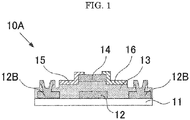
- FIG. 1 is a cross-sectional view exemplifying a field-effect transistor produced in the present disclosure.
- a field-effect transistor 10A is a bottom gate/bottom contact field-effect transistor including a substrate 11, a gate electrode 12, a gate insulating layer 13, an active layer 14, a source electrode 15, a drain electrode 16, and gate electrode pads 12B. Note that, the field-effect transistor 10A is one representative example of a semiconductor device according to the present disclosure.
- the gate electrode 12 and two gate electrode pads 12B are formed on the insulating substrate 11. Furthermore, the gate insulating layer 13 is formed so as to cover the gate electrode 12 and the two gate electrode pads 12B.
- the active layer 14 is formed on the gate insulating layer 13, and the source electrode 15 and the drain electrode 16 are formed on the active layer 14 so that channel is formed in the active layer 14.
- a side of the active layer 14 is considered as the upper side or one side, and a side of the substrate 11 is considered as the bottom side or the other side for the sake of convenience.
- a surface at a side of the active layer 14 is considered as the upper surface or one surface, and a surface at a side of the substrate 11 is considered as the bottom surface or the other surface.
- the field-effect transistor 10A can be used in a state of being turned upside down, or can be disposed at any angle.
- the planar view means seeing an object from a normal direction to the upper surface of the substrate 11.
- the planar shape means a shape of the object seen from the normal direction to the upper surface of the substrate 11.
- a shape, a structure, and a size of the substrate 11 are not particularly limited and may be appropriately selected depending on the intended purpose.
- a material of the substrate 11 is not particularly limited and may be appropriately selected depending on the intended purpose. As the material, glass substrates, ceramic substrates, plastic substrates, and film substrates can be used.
- the glass substrates are not particularly limited and may be appropriately selected depending on the intended purpose. Examples thereof include non-alkali glass and silica glass.
- the plastic substrates and film substrates are not particularly limited and may be appropriately selected depending on the intended purpose. Examples thereof include polycarbonate (PC), polyimide (PI), polyethylene terephthalate (PET), and polyethylene naphthalate (PEN).
- the gate electrode 12 is formed, for example, in a predetermined area on the substrate 11.
- the gate electrode 12 is an electrode to which gate voltage is to be applied.
- a material of the gate electrode 12 is not particularly limited and may be appropriately selected depending on the intended purpose.
- metals e.g., aluminum (Al), platinum (Pt), palladium (Pd), gold (Au), silver (Ag), copper (Cu), zinc (Zn), nickel (Ni), chromium (Cr), tantalum (Ta), molybdenum (Mo), and titanium (Ti)
- alloys thereof and mixtures of these metals
- conductive oxides e.g., indium oxide, zinc oxide, tin oxide, gallium oxide, and niobium oxide
- composite compounds thereof, and mixtures thereof may be used.
- An average film thickness of the gate electrode 12 is not particularly limited and may be appropriately selected depending on the intended purpose.
- the average film thickness thereof is preferably from 10 nm through 1 ⁇ m, more preferably from 50 nm through 300 nm.
- the gate electrode pads have the same layer as that of the gate electrode and are provided in order to contact, with the gate electrode, a probe for measurement when electrical characteristics are evaluated.
- the gate insulating layer 13 is a metal oxide.
- the gate insulating layer is provided between the gate electrode 12 and the active layer 14 in order to insulate the gate electrode 12 and the active layer 14.
- the metal oxide includes A element and at least one selected from the group consisting of B element and C element, and further includes other components if necessary.
- the A element is at least one selected from the group consisting of Sc, Y, Ln (lanthanoid), Sb, Bi, and Te.
- the B element is at least one selected from the group consisting of, Ga, Ti, Zr, and Hf.
- the C element is at least one selected from the group consisting of Group 2 elements in the periodic table.
- the metal oxide includes a paraelectric amorphous oxide or is formed with a paraelectric amorphous oxide itself.
- the paraelectric amorphous oxide is stable in the air and can stably form an amorphous structure in a broad formulation range.
- the metal oxide may partially include a crystal.
- Alkaline earth oxides easily react with moisture and carbon dioxide in the air, and are easily turned into hydroxides and carbonates. Therefore, the alkaline earth oxides alone are not suitable for applications to electronic devices. Furthermore, simple oxides of, for example, Ga, Sc, Y, and lanthanoid excluding Ce are easily turned into crystals, which is problematic in terms of generation of leakage current.
- metal oxides of the alkaline earth metals and Ga, Sc, Y, and lanthanoid excluding Ce are stable in the air, and can form an amorphous film in a broad formulation region. Ce becomes tetravalent specifically in the lanthanoid and forms a crystal having a perovskite structure together with the alkaline earth metal. Therefore, in order to obtain an amorphous phase, lanthanoid excluding Ce is preferable.
- crystalline phases such as a spinel structure exist between the alkaline earth metal and the Ga oxide, these crystals are not precipitated unless they are heated at a significantly high temperature (generally, at 1,000°C or more) compared to crystals having the perovskite structure.
- a significantly high temperature generally, at 1,000°C or more
- no report has been presented on existence of a stable crystalline phase between oxides of the alkaline earth metal and oxides of Sc, Y, and lanthanoid excluding Ce. Even after the post-process performed at a high temperature, the crystal is seldom precipitated from the amorphous phase.
- an amorphous phase becomes more stable when the metal oxides of the alkaline earth metal and Ga, Sc, Y, and lanthanoid excluding Ce are formed of three or more metal elements.
- An amount of each element contained in the metal oxide is not particularly limited. However, a metal element selected from each element group is preferably included so that the metal oxide has such formulation that can achieve a stable amorphous state.
- compositional ratios of elements such as Ba, Sr, Lu, and La be increased.
- the metal oxide according to the present embodiment can form an amorphous film in a broad formulation range, and thus its physical property can be broadly controlled.
- a dielectric constant thereof is sufficiently higher (i.e., from about 6 through about 20) than that of SiO 2 , but can be appropriately adjusted to a suitable value by selecting formulation depending on the intended purpose.
- a thermal expansion coefficient of the metal oxide is similar to those of the general materials of wired lines and general materials of semiconductors (i.e., from 10 -6 through 10 -5 ). Moreover, even when a heating step is repeated, the metal oxide causes less trouble such as exfoliation of the film compared to SiO 2 having a thermal expansion coefficient of 10 -7 or more but less than 10 -6 . Particularly, a favorable boundary between the metal oxide and the oxide semiconductor such as a-IGZO is formed.
- a method for forming the gate insulating layer is not particularly limited and may be appropriately selected depending on the intended purpose. Examples thereof include the following formation method using a coating liquid for forming insulating layer.
- the coating liquid for forming insulating layer includes, for example, at least A element-including compound, at least one selected from the group consisting of B element-including compound and C element-including compound, and a solvent, and further includes other components if necessary.
- the A element-including compound is not particularly limited and may be appropriately selected depending on the intended purpose, so long as the A element-including compound is a compound including at least one selected from the group consisting of Sc, Y, Ln (lanthanoid), Sb, Bi, and Te. Examples thereof include inorganic A element compounds and organic A element compounds.
- Examples of the inorganic A element compounds include nitrates of the A element, sulfates of the A element, fluorides of the A element, chlorides of the A element, bromides of the A element, and iodides of the A element.
- nitrates of the A element examples include scandium nitrate, yttrium nitrate, lanthanum nitrate, cerium nitrate, praseodymium nitrate, neodymium nitrate, samarium nitrate, europium nitrate, gadolinium nitrate, terbium nitrate, dysprosium nitrate, holmium nitrate, erbium nitrate, thulium nitrate, ytterbium nitrate, lutetium nitrate, antimony nitrate, bismuth nitrate, and tellurium nitrate.
- Examples of the sulfates of the A element include gallium sulfate, scandium sulfate, yttrium sulfate, lanthanum sulfate, cerium sulfate, praseodymium sulfate, neodymium sulfate, samarium sulfate, europium sulfate, gadolinium sulfate, terbium sulfate, dysprosium sulfate, holmium sulfate, erbium sulfate, thulium sulfate, ytterbium sulfate, lutetium sulfate, antimony sulfate, bismuth sulfate, and tellurium sulfate.
- Examples of the fluorides of the A element include scandium fluoride, yttrium fluoride, lanthanum fluoride, cerium fluoride, praseodymium fluoride, neodymium fluoride, samarium fluoride, europium fluoride, gadolinium fluoride, terbium fluoride, dysprosium fluoride, holmium fluoride, erbium fluoride, thulium fluoride, ytterbium fluoride, lutetium fluoride, antimony fluoride, bismuth fluoride, and tellurium fluoride.
- Examples of the chlorides of the A element include scandium chloride, yttrium chloride, lanthanum chloride, cerium chloride, praseodymium chloride, neodymium chloride, samarium chloride, europium chloride, gadolinium chloride, terbium chloride, dysprosium chloride, holmium chloride, erbium chloride, thulium chloride, ytterbium chloride, lutetium chloride, antimony chloride, bismuth chloride, tellurium chloride.
- bromides of the A element examples include scandium bromide, yttrium bromide, lanthanum bromide, praseodymium bromide, neodymium bromide, samarium bromide, europium bromide, gadolinium bromide, terbium bromide, dysprosium bromide, holmium bromide, erbium bromide, thulium bromide, ytterbium bromide, lutetium bromide, antimony bromide, bismuth bromide, and tellurium bromide.
- Examples of the iodides of the A element include scandium iodide, yttrium iodide, lanthanum iodide, cerium iodide, praseodymium iodide, neodymium iodide, samarium iodide, europium iodide, gadolinium iodide, terbium iodide, dysprosium iodide, holmium iodide, erbium iodide, thulium iodide, ytterbium iodide, lutetium iodide, antimony iodide, bismuth iodide, and tellurium iodide.
- the organic A element compound is not particularly limited and may be appropriately selected depending on the intended purpose, so long as the organic A element compound is a compound including the A element and an organic group.
- the A element and the organic group are bonded, for example, via an ionic bond, a covalent bond, or a coordinate bond.
- the organic group is not particularly limited and may be appropriately selected depending on the intended purpose.
- Examples of the organic group include alkyl groups which may have a substituent, alkoxy groups which may have a substituent, acyloxy groups which may have a substituent, acetyl acetonate groups which may have a substituent, and cyclopentadienyl groups which may have a substituent.
- Examples of the alkyl groups include alkyl groups including from 1 through 6 carbon atoms.
- Examples of the alkoxy groups include alkoxy groups including from 1 through 6 carbon atoms.
- Examples of the acyloxy groups include acyloxy groups including from 1 through 10 carbon atoms.
- Examples of the organic A element compound include scandium acetate, tris(cyclopentadienyl)scandium, yttrium isopropoxide, yttrium 2-ethylhexanoate, tris(acetylacetonato)yttrium, tris(cyclopentadienyl)yttrium, lanthanum isopropoxide, lanthanum 2-ethylhexanoate, tris(acetylacetonato)lanthanum, tris(cyclopentadienyl)lanthanum, cerium 2-ethylhexanoate, tris(acetylacetonato)cerium, tris(cyclopentadienyl)cerium, praseodymium isopropoxide, praseodymium oxalate, tris(acetylacetonato)praseodymium, tris(cyclopentadienyl)praseodymium, ne
- An amount of the A element-including compound in the coating liquid for forming insulating layer is not particularly limited and may be appropriately selected depending on the intended purpose.
- the B element-including compound is not particularly limited and may be appropriately selected depending on the intended purpose, so long as the B element-including compound is a compound including at least one selected from the group consisting of Ga, Ti, Zr, and Hf. Examples thereof include inorganic B element compounds and organic B element compounds.
- examples of the inorganic B element compounds include gallium nitrate, gallium sulfate, gallium fluoride, gallium chloride, gallium bromide, gallium iodide, gallium hydroxide, titanium sulfide, titanium fluoride, titanium chloride, titanium bromide, titanium iodide, zirconium sulfate, zirconium carbonate, zirconium fluoride, zirconium chloride, zirconium bromide, zirconium iodide, hafnium sulfate, hafnium fluoride, hafnium chloride, hafnium bromide, and hafnium iodide.
- the organic B element compound is not particularly limited and may be appropriately selected depending on the intended purpose, so long as the organic B element compound is a compound including the B element and an organic group.
- the B element and the organic group are bonded, for example, via an ionic bond, a covalent bond, or a coordinate bond.
- the organic group is not particularly limited and may be appropriately selected depending on the intended purpose.
- Examples of the organic group include alkyl groups which may have a substituent, alkoxy groups which may have a substituent, acyloxy groups which may have a substituent, acetylacetonate groups which may have a substituent, and cyclopentadienyl groups which may have a substituent.
- Examples of the alkyl groups include alkyl groups including from 1 through 6 carbon atoms.
- Examples of the alkoxy groups include alkoxy groups including from 1 through 6 carbon atoms.
- Examples of the acyloxy groups include acyloxy groups including from 1 through 10 carbon atoms.
- organic B element compounds include tris(cyclopentadienyl)gallium, scandium isopropoxide, titanium isopropoxide, bis(cyclopentadienyl)titanium chloride, zirconium butoxide, zirconium isopropoxide, bis(2-ethylhexanoate)zirconium oxide, zirconium di(n-butoxide)bisacetylacetonato, tetrakis(acetylacetonate)zirconium, tetrakis(cyclopentadienyl)zirconium, hafnium butoxide, hafnium isopropoxide, tetrakis(2-ethylhexanoate)hafnium, hafnium di(n-butoxide)bisacetylacetonato, tetrakis(acetylacetonate)hafnium, and bis(cydopentadienyl)d
- An amount of the B element-including compound in the coating liquid for forming insulating layer is not particularly limited and may be appropriately selected depending on the intended purpose.
- the C element-including compound is not particularly limited and may be appropriately selected depending on the intended purpose, so long as the C element-including compound is a compound including at least one selected from the group consisting of Group 2 elements in the periodic table.
- Examples thereof include inorganic alkaline earth metal compounds and organic alkaline earth metal compounds.
- alkaline earth metals in the alkaline-earth-metal-including compounds include Be (beryllium), Mg (magnesium), Ca (calcium), Sr (strontium), and Ba (barium).
- Examples of the inorganic alkaline earth metal compounds include alkaline earth metal nitrates, alkaline earth metal sulfates, alkaline earth metal chlorides, alkaline earth metal fluorides, alkaline earth metal bromides, and alkaline earth metal iodides.
- alkaline earth metal nitrates examples include magnesium nitrate, calcium nitrate, strontium nitrate, and barium nitrate.
- alkaline earth metal sulfates examples include magnesium sulfate, calcium sulfate, strontium sulfate, and barium sulfate.
- alkaline earth metal chlorides examples include magnesium chloride, calcium chloride, strontium chloride, and barium chloride.
- alkaline earth metal fluorides examples include magnesium fluoride, calcium fluoride, strontium fluoride, and barium fluoride.
- alkaline earth metal bromides examples include magnesium bromide, calcium bromide, strontium bromide, and barium bromide.
- alkaline earth metal iodides examples include magnesium iodide, calcium iodide, strontium iodide, and barium iodide.
- the organic alkaline earth metal compound is not particularly limited and may be appropriately selected depending on the intended purpose, so long as the organic alkaline earth metal compound is a compound including an alkaline earth metal and an organic group.
- the alkaline earth metal and the organic group are bonded, for example, via an ionic bond, a covalent bond, or a coordinate bond.
- the organic group is not particularly limited and may be appropriately selected depending on the intended purpose.
- Examples of the organic group include alkyl groups which may have a substituent, alkoxy groups which may have a substituent, acyloxy groups which may have a substituent, phenyl groups which may have a substituent, acetyl acetonate groups which may have a substituent, and sulfonic acid groups which may have a substituent.
- alkyl groups include alkyl groups including from 1 through 6 carbon atoms.
- Examples of the alkoxy groups include alkoxy groups including from 1 through 6 carbon atoms.
- acyloxy groups include: acyloxy groups including from 1 through 10 carbon atoms; acyloxy groups part of which is substituted with a benzene ring, such as benzoic acid; acyloxy groups part of which is substituted with a hydroxyl group, such as lactic acid; and acyloxy groups including two or more carbonyl groups, such as oxalic acid and citric acid.
- organic alkaline earth metal compounds examples include magnesium methoxide, magnesium ethoxide, diethyl magnesium, magnesium acetate, magnesium formate, acetylacetone magnesium, magnesium 2-ethylhexanoate, magnesium lactate, magnesium naphthenate, magnesium citrate, magnesium salicylate, magnesium benzoate, magnesium oxalate, magnesium trifluromethanesulfonate, calcium methoxide, calcium ethoxide, calcium acetate, calcium formate, acetylacetone calcium, calcium dipivaloyl methanate, calcium 2-ethylhexanoate, calcium lactate, calcium naphthenate, calcium citrate, calcium salicylate, calcium neodecanoate, calcium benzoate, calcium oxalate, strontium isopropoxide, strontium acetate, strontium formate, acetylacetone strontium, strontium 2-ethylhexanoate, strontium lactate, strontium naph
- An amount of the C element-including compound in the coating liquid for forming insulating layer is not particularly limited and may be appropriately selected depending on the intended purpose.
- the solvent is not particularly limited and may be appropriately selected depending on the intended purpose, so long as the solvent is capable of stably dissolving or dispersing the above various compounds.
- the solvent include toluene, xylene, mesitylene, cymene, pentylbenzene, dodecylbenzene, bicyclohexyl, cyclohexylbenzene, decane, undecane, dodecane, tridecane, tetradecane, pentadecane, tetralin, decalin, isopropanol, ethyl benzoate, N,N-dimethylformamide, propylene carbonate, 2-ethylhexanoic acid, mineral spirits, dimethylpropylene urea, 4-butyrolactone, 2-methoxy ethanol, propylene glycol, and water.
- An amount of the solvent in the coating liquid for forming insulating layer is not particularly limited and may be appropriately selected depending on the intended purpose.
- the formation method of the gate insulating layer includes a coating step and a heat treatment step, and further includes other steps if necessary.
- the coating step is not particularly limited and may be appropriately selected depending on the intended purpose, so long as the coating step is a step of coating the coating liquid for forming insulating layer on an object to be coated.
- the coating method is not particularly limited and may be appropriately selected depending on the intended purpose. Examples of the solution process include dip coating, spin coating, die coating, and nozzle printing.
- the heat treatment step is not particularly limited and may be appropriately selected depending on the intended purpose, so long as the heat treatment step is a step of subjecting, to a heat treatment, the coating liquid for forming insulating layer coated on the object to be coated.
- the coating liquid for forming insulating layer coated on the object to be coated may be dried through, for example, air-drying. Through the heat treatment, the solvent is dried and the metal oxide is produced.
- drying treatment drying of the solvent
- generation treatment generation of the metal oxide
- a temperature of the drying treatment is not particularly limited and may be appropriately selected depending on the solvent contained.
- the temperature of the drying treatment is from 80°C through 180°C.
- it is effective to use a vacuum oven for reducing the temperature.
- the time of the drying treatment is not particularly limited and may be appropriately selected depending on the intended purpose. For example, the time of the drying treatment is from 1 minute through 1 hour.
- a temperature of the generation treatment is not particularly limited and may be appropriately selected depending on the intended purpose.
- the temperature of the generation treatment is preferably 100°C or higher but lower than 550°C, more preferably from 200°C through 500°C.
- the time of the generation treatment is not particularly limited and may be appropriately selected depending on the intended purpose. For example, the time of the generation treatment is from 1 hour through 5 hours.
- the drying treatment and the generation treatment may be continuously performed or may be performed in a divided manner of a plurality of steps.
- a temperature of the generation treatment may affect etching rates of various etching solutions in some cases. Therefore, in order to control the etching rate, the heat treatment may be performed at a temperature higher than the temperature of the generation treatment, after patterning.
- a method of the heat treatment is not particularly limited and may be appropriately selected depending on the intended purpose.
- Examples of the method of the heat treatment include a method of heating the object to be coated.
- An atmosphere in the heat treatment is not particularly limited and may be appropriately selected depending on the intended purpose. However, the atmosphere is preferably an oxygen atmosphere. When the heat treatment is performed in the oxygen atmosphere, decomposed products can be promptly discharged outside the system and generation of the metal oxide can be accelerated.
- the heat treatment in view of acceleration of reaction of the generation treatment, it is effective to irradiate, with ultraviolet rays having a wavelength of 400 nm or shorter, the material that has undergone the drying treatment. Irradiation of the ultraviolet rays having a wavelength of 400 nm or shorter can cleave chemical bonds of the organic material contained in the material that has undergone the drying treatment, and can decompose the organic material. Therefore, the metal oxide can be efficiently formed.
- the ultraviolet rays having a wavelength of 400 nm or shorter are not particularly limited and may be appropriately selected depending on the intended purpose. Examples of the ultraviolet rays include ultraviolet rays having a wavelength of 222 nm emitted from an excimer lamp. It is also preferable to apply ozone instead of or in combination with irradiation of the ultraviolet rays. Applying the ozone to the material that has undergone the drying treatment accelerates generation of the metal oxide.
- a film thickness of the gate insulating layer formed on the electrodes may be thick in terms of coverage, withstand pressure, and reduction in leak current, or may be thin in such a range that can maintain insulation property in terms of capacity of the gate insulating layer.
- the film thickness thereof can be appropriately selected depending on the intended purpose, but is preferably from 10 nm through 3 ⁇ m, more preferably from 30 nm through 1 ⁇ m.
- the gate insulating layer may have a plurality of layers, and a film of the gate insulating layer is formed by separately forming each of the plurality of layers several times.
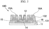
- the gate insulating layer may be appropriately adjusted so as to satisfy the aforementioned film thickness (for example, the total value of the gate insulating layer 131 and the gate insulating layer 132 in FIG. 5 , which will be described hereinafter).
- the gate insulating layer 131 may have a plurality of layers, and may be appropriately adjusted so as to satisfy the aforementioned film thickness (for example, the gate insulating layer 131 is formed through coating several times in FIG. 9 , which will be described hereinafter, and may be adjusted so as to satisfy the aforementioned film thickness).
- a material of the active layer 14 is not particularly limited and may be appropriately selected depending on the intended purpose. Examples thereof include organic semiconductors such as polycrystal silicon (p-Si), amorphous silicon (a-Si), an oxide semiconductor, and pentacene. Among them, use of an oxide semiconductor is preferable in terms of safety of boundary between the active layer 14 and the gate insulating layer 13.
- the active layer 14 is, for example, an active layer configured to form channel between the source electrode and the drain electrode when a predetermined voltage is applied to the gate electrode.
- the active layer 14 can be formed by, for example, an n-type oxide semiconductor.
- the n-type oxide semiconductor constituting the active layer 14 is not particularly limited and may be appropriately selected depending on the intended purpose.
- the n-type oxide semiconductor preferably includes: at least one selected from the group consisting of indium (In), Zn, tin (Sn), and Ti; and an alkaline earth element or a rare earth element, more preferably includes In and an alkaline earth element or a rare earth element.
- rare earth element examples include scandium (Sc), yttrium (Y), lanthanum (La), cerium (Ce), praseodymium (Pr), neodymium (Nd), promethium (Pm), samarium (Sm), europium (Eu), gadolinium (Gd), terbium (Tb), dysprosium (Dy), holmium (Ho), erbium (Er), thulium (Tm), ytterbium (Yb), and lutetium (Lu).
- Indium oxide changes a concentration of electron carriers from about 10 18 cm -3 to about 10 20 cm -3 depending on the amount of oxygen vacancies.
- indium oxide has a property that easily generates oxygen vacancies, and may generate unexpected oxygen vacancies in a post process after formation of the oxide semiconductor film in some cases.
- the oxide is particularly preferably formed of mainly two metals: indium; and an alkaline earth element or rare earth element that is easily bound to oxygen compared to indium. The reason for this is because unexpected oxygen vacancies can be prevented and control of the formation becomes easy to appropriately control the concentration of electron carriers.
- the n-type oxide semiconductor constituting the active layer 14 undergoes substitutional doping with at least one dopant selected from the group consisting of a divalent cation, a trivalent cation, a tetravalent cation, a pentavalent cation, a hexavalent cation, a heptavalent cation, and an octavalent cation, and a valence of the dopant is more than a valence of the metal ion constituting the n-type oxide semiconductor (provided that the dopant is excluded from the metal ion).
- the substitutional doping may be referred to as an n-type doping.
- the source electrode 15 and the drain electrode 16 are formed on the gate insulating layer 13.
- the source electrode 15 and the drain electrode 16 are formed so that a predetermined spacing is provided therebetween.
- the source electrode 15 and the drain electrode 16 are electrodes configured to take electric current out correspondingly to application of gate voltage to the gate electrode 12.
- a wired line connected to the source electrode 15 and the drain electrode 16 may be formed on the same layer, together with the source electrode 15 and the drain electrode 16.
- a material of the source electrode 15 and the drain electrode 16 is not particularly limited and may be appropriately selected depending on the intended purpose.
- the material thereof is preferably a material capable of etching using the etching solution A having the same type as the etching solution B.
- Such a material is not particularly limited and may be appropriately selected depending on the intended purpose, so long as it is selected from the group consisting of metals that can be etched using the etching solution A, alloys, mixtures of a plurality of metals, conductive oxides, composite compounds, and stacked films of metals and conductive oxides.
- metals such as aluminum (Al) and molybdenum (Mo), alloys thereof, and mixtures of these metals can be used.
- conductive oxides such as indium oxide and zinc oxide, composite compounds thereof, and mixtures thereof may be used.
- the conductive oxides, the composite compounds, the mixtures thereof can be used irrespective of being multicrystal and amorphous.
- the conductive oxides, the composite compounds, the mixtures are preferably amorphous in a patterning process, because an amorphous structure reduces variations of an etching rate on the same substrate and patterning with favorable precision can be achieved. It is known that these materials are subjected to a heat treatment in order to improve conductive property of the electrodes. However, the heat treatment is preferably performed after patterning in terms of precision of patterning.
- ITO tin-doped indium oxide
- IZO In 2 O 3 -ZnO complex oxide
- IZO is more preferable when patterning is performed because it is amorphous and stable.
- a metal having a high conductivity is preferably stacked considering resistance of wired lines.
- the metal having a high conductivity include Ag, Al, and Cu.
- conductive oxides, the composite compounds, and the mixtures thereof stacked using the etching solution having the same type can be preferably etched at once.
- An average film thickness of the source electrode 15 and the drain electrode 16 is not particularly limited and may be appropriately selected depending on the intended purpose.
- the average film thickness thereof is preferably from 10 nm through 1 ⁇ m, more preferably from 50 nm through 300 nm.
- a method for forming patterns of each layer of the formed film As a method for forming patterns of each layer of the formed film, a method for forming patterns through photolithography and etching is generally used.
- the etching method can be appropriately selected from dry etching and wet etching depending on the intended purpose. However, wet etching is preferable in terms of production cost.
- the etching solution used in the wet etching can be selected depending on the respective layers. However, the larger the number of layers obtained using the etching solution having the same type is, the lower the production cost is, which is preferable.
- vacuum process it is necessary to distinguish process chambers for each layer, in order to prevent occurrence of contamination.
- chambers used are preferably distinguished as chambers for the metal and chambers for the oxide.
- the metal-based process may be applied as it is.
- the etching solution having the same type as those used for etching at least the gate insulating layer and the active layer is preferably applied to a layer using wet etching.
- etching solution A examples include etching solutions including nitric acid, etching solutions including hydrogen peroxide, and etching solutions including oxalic acid.
- Examples of the etching solution B that is an etching solution having the same type as the etching solution A are as follows, for example. Specifically, when the etching solution A is an etching solution including nitric acid, the etching solution B is an etching solution including nitric acid. When the etching solution A is an etching solution including hydrogen peroxide, the etching solution B is an etching solution including hydrogen peroxide. When the etching solution A is an etching solution including oxalic acid, the etching solution B is an etching solution including oxalic acid.
- concentrations of the etching solution A and the etching solution B may be the same or different, so long as the etching solution A and the etching solution B have the same main component contributing to etching.
- other constituent components in the etching solution A and the etching solution B may be the same or different, so long as the etching solution A and the etching solution B have the same main component contributing to etching.
- the etching solution A is the etching solution including nitric acid
- the etching solution A preferably further includes phosphoric acid and acetic acid.
- the etching solution B is the etching solution including nitric acid
- the etching solution B preferably further includes phosphoric acid and acetic acid.
- the metal oxide of the present disclosure functions as the gate insulating layer of the field-effect transistor.
- the metal oxide includes A element and at least one selected from the group consisting of B element and C element.
- the A element is at least one selected from the group consisting of Sc, Y, Ln (lanthanoid), Sb, Bi, and Te. Details and preferable aspects of the A element are the same as the details and the preferable aspects in the description of the field-effect transistor.
- the B element is at least one selected from the group consisting of Ga, Ti, Zr, and Hf. Details and preferable aspects of the B element are the same as the details and the preferable aspects in the description of the field-effect transistor.
- the C element is at least one selected from the group consisting of Group 2 elements in a periodic table. Details and preferable aspects of the C element are the same as the details and the preferable aspects in the description of the field-effect transistor.
- an etching rate of the metal oxide in a wet etching solution including nitric acid is 0.1 nm/s or more but 20 nm/s or less, preferably 0.1 nm/s or more but 10 nm/s or less, more preferably 0.5 nm/s or more but 5 nm/s or less.
- a temperature of the wet etching solution is generally 35°C.
- the etching rate is generally an etching rate obtained when the metal oxide is immersed into the wet etching solution, followed by light stirring.
- the etching depth can be determined by, for example, observing it with a transmission electron microscope. In the case of the evaluation of a single film or the evaluation of an uppermost layer during the process for producing the device, the etching depth can be easily determined by measuring a shape of steps using an atomic force microscope.
- the wet etching solution is, for example, a wet etching solution including 6% by mass of nitric acid.
- the wet etching solution is, for example, a wet etching solution including 6% by mass of nitric acid, 25% by mass of acetic acid, and 50% by mass of phosphoric acid.
- the wet etching solution is, for example, a wet etching solution used for forming at least one selected from the group consisting of the active layer, the gate electrode, and the source electrode and the drain electrode after formation of the gate insulating layer in production of the field-effect transistor.
- the at least one selected from the group consisting of the active layer, the gate electrode, and the source electrode and the drain electrode is in contact with the gate insulating layer.
- etching solution having the same type is effective in the formation of the gate insulating layer and the formation of at least one selected from the group consisting of the active layer, the gate electrode, and the source electrode and the drain electrode for the purpose of reducing production cost. Furthermore, an etching rate is important in terms of the TAKT time and the processing shape. Particularly, regarding the gate insulating layer, it is preferable that an etching rate in the etching solution in the formation of at least one selected from the group consisting of the active layer, the gate electrode, and the source electrode and the drain electrode be considered.
- an etching rate of the metal oxide in the wet etching solution including nitric acid is 0.1 nm/s or more.
- etching time is prolonged in the case of overetching the gate insulating layer that generally has a film thickness of from about 100 nm through about 300 nm in order to perform patterning without residues.
- the TAKT time is prolonged.
- the wet etching solution including nitric acid is used to form the gate electrode after the gate insulating layer is formed, when the etching rate is less than 0.1 nm/s, the TAKT time is prolonged likewise.
- an etching rate of the metal oxide in the wet etching solution including nitric acid is 20 nm/s or less.
- the wet etching solution including nitric acid is used to form the gate electrode after formation of the gate insulating layer
- the etching rate is more than 20 nm/s
- a portion of the gate insulating layer, the portion underlying the gate electrode is considerably etched from a boundary between the gate electrode and the underlying gate insulating layer.
- line width of the gate insulating layer underlying the gate electrode easily becomes thinner than line width of the gate electrode (undercut).
- the portion underlying the gate electrode is completely etched, which results in failure in patterning such as the exfoliated gate electrode.
- occurrence of this state will be described with reference to specific examples.
- the precondition is following. Specifically, when an etching rate of the gate insulating layer is more than 20 nm/s, the etching rate thereof is generally faster than an etching rate of the gate electrode.
- Mo having an etching rate of 6 nm/s is used to form the gate electrode having a film thickness of 100 nm, it takes 17 seconds to etch Mo by 100 nm.
- the overetching time: about 8 s and the etching rate of the gate insulating layer: 20 nm/s the gate insulating layer is etched by 160 nm.
- a simple calculation will be performed in terms of design of width of the gate electrode.
- the wet etching is an isotropic etching. Therefore, as the etching proceeds by 160 nm in a direction of the film thickness, the portion underlying the gate electrode is also etched by 160 nm toward a direction of the in-plane direction: i.e. a direction of an inner side of the pattern of the gate electrode.
- the width of the gate electrode is 10 ⁇ m
- the required etching time is etching time of the gate insulating layer ⁇ 1.5 times
- the width of the gate insulating layer is 9.52 ⁇ m (10 ⁇ m-0.24 ⁇ m ⁇ 2) and becomes thinner than the width of the gate electrode by about 5%.
- an etching rate of Al is twice as high as that of Mo.
- the width of the gate insulating layer that is the base portion of the gate electrode is about 9 ⁇ m, and becomes thinner than the width of the gate electrode by 10%.
- the designed value of the width of the gate electrode is thinner (high precision), such a state that the undercut proceeds is found even for the same etching time. As a result, an edge of the pattern of the gate electrode is raised, warped, or exfoliated.
- the metal oxide is used in the gate insulating layer.
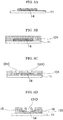
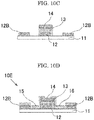
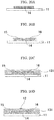
- FIG. 2A to FIG. 2E are views exemplifying production steps of the field-effect transistor 10A according to an embodiment.
- a substrate 11 formed of, for example, a glass substrate is provided.
- a conductive film formed of, for example, aluminum (Al) is formed on the substrate 11 through the sputtering method, and the formed conductive film is patterned through photolithography and etching to form a gate electrode 12 and gate electrode pads 12B having predetermined shapes.
- a pre-treatment such as oxygen plasma, UV ozone, or UV radiation washing is preferably performed before the gate electrode 12 and the gate electrode pads 12B are formed. Materials and thicknesses of the substrate 11, the gate electrode 12, and the gate electrode pads 12B can be appropriately selected.
- a method for producing the gate electrode 12 and the gate electrode pads 12B is not particularly limited and may be appropriately selected depending on the intended purpose.
- One exemplary method is, for example, a method of forming a film through, for example, a sputtering method, a vacuum deposition method, a dip coating method, a spin coating method, or a die coating method, and then patterning the film through photolithography.
- Another example is, for example, a method of directly forming a film having a desired shape through a printing process such as inkjet printing, nanoimprinting, or gravure printing.
- a method for forming the gate insulating layer 13 is not particularly limited and may be appropriately selected depending on the intended purpose. Examples thereof include: film formation steps through a vacuum process (e.g., a sputtering method, a pulsed laser deposition (PLD) method, a chemical vapor deposition (CVD) method, or an atomic layer deposition (ALD) method) or film formation steps through a solution process (e.g., dip coating, spin coating, or die coating). Another example thereof is, for example, a printing process such as inkjet printing, nanoimprinting, or gravure printing. A material and thickness of the gate insulating layer 13 can be appropriately selected as described above.
- a vacuum process e.g., a sputtering method, a pulsed laser deposition (PLD) method, a chemical vapor deposition (CVD) method, or an atomic layer deposition (ALD) method
- a solution process e.g., dip coating, spin coating, or die coating
- a printing process such
- through holes 13C are formed by etching the gate insulating layer 13 on the gate electrode pads 12B.
- PAN-based etching solution etching solution including phosphoric acid, acetic acid, and nitric acid
- etching solution having the same type as the etching solution for subjecting the gate electrode 12 to wet etching it is possible to sufficiently obtain an etching selection ratio between the gate electrode 12 and the gate insulating layer 13, by incorporating polycrystalline ITO that is the conductive oxide into the uppermost layer of the gate electrode 12.
- through holes 13C are formed by etching the gate insulating layer 13 on the gate electrode pads 12B.
- the PAN-based etching solution is used as an etching solution having the same type as the etching solution for subjecting the gate electrode 12 to wet etching
- the etching rate of the gate electrode in the PAN-based etching solution is large, it is possible to sufficiently obtain an etching selection ratio between the gate electrode pads 12B and the gate insulating layer 13, by including polycrystalline ITO that is the conductive oxide in the uppermost layer of the gate electrode pads 12B, or using Al, an Al alloy, Ti, or W in the uppermost layer of the electrode pads 12B, in order to protect the electrode pads 12B.
- a film of the oxide semiconductor is formed so as to cover the gate electrode pads 12B, the through holes 13C, and the gate insulating layer 13.
- the formed oxide semiconductor is patterned through photolithography and wet etching to form an active layer 14 having a predetermined shape.
- a film formation method of the oxide semiconductor is not particularly limited and may be appropriately selected depending on the intended purpose. Examples thereof include: film formation steps through a vacuum process (e.g., a sputtering method, a pulsed laser deposition (PLD) method, a chemical vapor deposition (CVD) method, or an atomic layer deposition (ALD) method) or film formation steps through a solution process (e.g., dip coating, spin coating, or die coating).
- the oxide semiconductor can be formed of, for example, an n-type oxide semiconductor.
- the etching solution used for etching the etching solution having the same type as the etching solution for subjecting the gate insulating layer 13 to etching can be used. However, the following (i) or (ii) is caused depending on the etching rate of the oxide semiconductor and the etching rate of the gate insulating layer in the etching solution of the oxide semiconductor.
- FIG. 2D is an example where a step having the same shape as that of the active layer 14 is formed on the gate insulating layer 13 depending on the etching rate of the oxide semiconductor.
- the active layer 14 formed may include crystalline components and amorphous components. However, in order not completely dissolve the gate insulating layer 13 upon the wet etching, it is preferable that an amount of the amorphous components be large upon forming patterns for the purpose of obtaining a selection ratio of the etching rate between the active layer 14 and the gate insulating layer 13.
- a conductive film to become a source electrode 15 and a drain electrode 16 is formed over the whole surface on the gate electrode pads 12B, the through holes 13C, the gate insulating layer 13, and the active layer 14. Then, the formed conductive film is patterned through photolithography and wet etching to form the source electrode 15 and the drain electrode 16 each having a predetermined shape.
- a pre-treatment such as oxygen plasma, UV ozone, or UV radiation washing is preferably performed before formation of the conductive film to become the source electrode 15 and the drain electrode 16.
- a formation method of the conductive film to become the source electrode 15 and the drain electrode 16 is not particularly limited and may be appropriately selected depending on the intended purpose.
- One exemplary method is, for example, a method of forming a film through, for example, a sputtering method, a vacuum deposition method, a dip coating method, a spin coating method, or a die coating method, and then patterning the film through photolithography.
- Another example thereof is, for example, a printing process such as inkjet printing, nanoimprinting, or gravure printing. Materials to become the source electrode 15 and the drain electrode 16 and thicknesses thereof can be appropriately selected as described in the above description regarding the source electrode 15 and the drain electrode 16.
- an etching solution having the same type as the etching solution that has etched the gate insulating layer 13 can be used as the etching solution used for subjecting, to wet etching, the conductive film to become the source electrode 15 and the drain electrode 16, an etching solution having the same type as the etching solution that has etched the gate insulating layer 13 can be used.
- steps having the same shape as those of the source electrode 15 and the drain electrode 16 may be generated on the gate insulating layer 13 depending on etching rates of the conductive film to become the source electrode 15 and the drain electrode 16, but the gate insulating layer 13 is not completely dissolved.
- an etching rate of the source electrode 15 and the drain electrode 16 is preferably faster than the etching rate of the gate insulating layer 13 by about 10 folds.
- the active layer 14 is also etched when the source electrode 15 and the drain electrode 16 are formed. However, it is preferable that the active layer 14 be subjected to a heat treatment beforehand, to thereby obtain a sufficient selection ratio of the etching rate between the active layer 14 and the conductive film to become the source electrode 15 and the drain electrode 16.
- etching is further performed for the purpose of disconnecting electrical connection between the source electrode 15 and the gate electrode pad 12B at a side of the source electrode 15, and electrical connection between the drain electrode 16 and the gate electrode pad 12B at a side of the drain electrode 16.
- a bottom gate/top contact field-effect transistor 10A can be produced.
- a variation example of an embodiment presents an example of a top gate/top contact field-effect transistor.
- the description of the same constituent parts as those that have been previously described in the embodiment may be omitted in some cases.
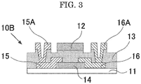
- FIG. 3 is a cross-sectional view exemplifying a field-effect transistor according to the variation example of the embodiment.
- a field-effect transistor 10B is a top gate/top contact field-effect transistor. Note that, the field-effect transistor 10B is one representative example of a semiconductor device according to the present disclosure.
- the field-effect transistor 10B has a layer structure different from that of the field-effect transistor 10A (see FIG. 1 ).
- the field-effect transistor 10B includes: a substrate 11; an active layer 14 formed on the substrate 11; a source electrode 15 and a drain electrode 16 formed on the active layer 14; a gate insulating layer 13 formed on the active layer 14, and the source electrode 15 and the drain electrode 16; and a gate electrode 12 formed on the gate insulating layer 13.
- the etching solutions having the same type are used at least when the gate insulating layer 13 is etched and when the gate electrode 12 is formed.
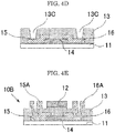
- FIG. 4A to FIG. 4E are views exemplifying production steps of the field-effect transistor 10B according to an embodiment.
- a substrate 11 formed of, for example, a glass substrate is provided. Then, a film of an oxide semiconductor is formed on the substrate 11, and the formed oxide semiconductor is patterned through photolithography and wet etching to form an active layer 14 having a predetermined shape.
- a conductive film to become a source electrode 15 and a drain electrode 16 is formed over the whole surface on the substrate 11 and the active layer 14, and the formed conductive film is patterned through photolithography and wet etching to form the source electrode 15 and the drain electrode 16 each having a predetermined shape.
- the gate insulating layer 13 on the source electrode 15 and the drain electrode 16 is etched to form through holes 13C.
- an etching solution having the same type as the etching solution for subjecting, to wet etching, the active layer 14, or the source electrode 15 and the drain electrode 16 is used.
- a conductive film to become a gate electrode 12, a source wired line 15A connecting the source electrode 15 to the outside, and a drain wired line 16A connecting the drain electrode 16 to the outside is formed over the whole surface on the exposed source electrode 15, the exposed drain electrode 16, and the gate insulating layer 13.
- the formed conductive film is patterned through photolithography and wet etching to form the gate electrode 12, the source wired line 15A, and the drain wired line 16A each having a predetermined shape.
- etching is further performed for the purpose of disconnecting electrical connection between the source wired line 15A and the gate electrode 12, and electrical connection between the drain wired line 16A and the gate electrode 12.
- a top gate/top contact field-effect transistor 10B can be produced.
- a variation example of an embodiment presents an example of a top gate/top contact field-effect transistor.
- the description of the same constituent parts as those that have been previously described in the embodiment may be omitted in some cases.
- a field-effect transistor 10C is a top gate/top contact field-effect transistor. Note that, the field-effect transistor 10C is one representative example of a semiconductor device according to the present disclosure.
- the field-effect transistor 10C has a layer structure different from that of the field-effect transistor 10B (see FIG. 3 ).
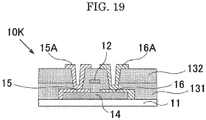
- the field-effect transistor 10C includes: a substrate 11; an active layer 14 formed on the substrate 11; a first gate insulating layer 131 formed on the active layer 14; a source electrode 15 and a drain electrode 16 that are in contact with the active layer 14 via through holes 131C formed on the first gate insulating layer 131; a second gate insulating layer 132 formed on the source electrode 15 and the drain electrode 16; and a gate electrode 12 formed on the second gate insulating layer 132.
- the etching solutions having the same type are used both when at least one of the first gate insulating layer 131 and the second gate insulating layer 132 is etched and when at least one of the source electrode 15 and drain electrode 16, and the gate electrode 12 is formed.
- At least one of the first gate insulating layer 131 and the second gate insulating layer 132 is the metal oxide.
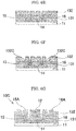
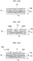
- FIG. 6A to FIG. 6E are views exemplifying production steps of the field-effect transistor 10C according to an embodiment.
- a substrate 11 formed of, for example, a glass substrate is provided. Then, a film of an oxide semiconductor is formed on the substrate 11, and the formed oxide semiconductor is patterned through photolithography and wet etching to form an active layer 14 having a predetermined shape.
- a first gate insulating layer 131 which covers the substrate 11 and the active layer 14, is formed.
- the first gate insulating layer 131 is etched to form through holes 131C in order to form a source electrode 15 and a drain electrode 16.
- an etching solution having the same type as the etching solution for subjecting, to wet etching, the active layer 14, or the source electrode 15 and the drain electrode 16 is used.
- a conductive film to become the source electrode 15 and the drain electrode 16 is formed on the first gate insulating layer 131 and the exposed active layer 14.
- the formed conductive film is patterned through photolithography and wet etching to form the source electrode 15 and the drain electrode 16 each having a predetermined shape.
- a second gate insulating layer 132 is formed on the first gate insulating layer 131, and the source electrode 15 and the drain electrode 16.
- the second gate insulating layer 132 is etched to form through holes 132C in order to form a source wired line 15A and a drain wired line 16A.
- an etching solution having the same type as the etching solution for subjecting, to wet etching, the active layer 14, or the source electrode 15 and the drain electrode 16 is used.
- a conductive film to become a gate electrode 12, a source wired line 15A, and a drain wired line 16A is formed over the whole surface on the exposed source electrode 15, the exposed drain electrode 16, and the second gate insulating layer 132.
- the formed conductive film is patterned through photolithography and wet etching to form the gate electrode 12, the source wired line 15A, and the drain wired line 16A each having a predetermined shape.
- etching is further performed for the purpose of disconnecting electrical connection between the source wired line 15A and the gate electrode 12, and electrical connection between the drain wired line 16A and the gate electrode 12.
- a top gate/top contact field-effect transistor 10C can be produced.
- a variation example of an embodiment presents an example of a top gate/top contact field-effect transistor.
- the description of the same constituent parts as those that have been previously described in the embodiment may be omitted in some cases.
- a field-effect transistor 10D is a top gate/top contact field-effect transistor. Note that, the field-effect transistor 10D is one representative example of a semiconductor device according to the present disclosure.
- the field-effect transistor 10D has a layer structure different from that of the field-effect transistor 10B (see FIG. 3 ).
- the field-effect transistor 10D includes: a substrate 11; an active layer 14 formed on the substrate 11; a first gate insulating layer 131 formed on the active layer 14; a source electrode 15 and a drain electrode 16 that are in contact with the active layer 14 via through holes 131C formed on the first gate insulating layer 131; a second gate insulating layer 132 formed on the source electrode 15 and the drain electrode 16; and a gate electrode 12 formed on the second gate insulating layer 132.
- the etching solutions having the same type are used both when at least one of the first gate insulating layer 131 and the second gate insulating layer 132 is etched and when at least one of the source electrode 15 and the drain electrode 16, and the gate electrode 12 is formed.
- At least one of the first gate insulating layer 131 and the second gate insulating layer 132 is preferably the metal oxide, both of them are more preferably the metal oxide.
- FIG. 8A to FIG. 8G are views exemplifying production steps of the field-effect transistor 10C according to an embodiment.
- a substrate 11 formed of, for example, a glass substrate is provided. Then, a film of an oxide semiconductor is formed on the substrate 11, and the formed oxide semiconductor is patterned through photolithography and wet etching to form an active layer 14 having a predetermined shape.
- a first gate insulating layer 131 which covers the substrate 11 and the active layer 14, is formed.
- the first gate insulating layer 131 is etched to form through holes 131C in order to form a source electrode 15 and a drain electrode 16.
- an etching solution having the same type as the etching solution for subjecting, to wet etching, the active layer 14, or the source electrode 15 and the drain electrode 16 is used.
- a conductive film to become the source electrode 15 and the drain electrode 16 is formed on the first gate insulating layer 131 and the exposed active layer 14.
- the formed conductive film is patterned through photolithography and wet etching to form the source electrode 15 and the drain electrode 16 each having a predetermined shape.
- the source electrode 15 and the drain electrode 16 are formed.
- the first gate insulating layer 131 on the active layer 14 and a region of the first gate insulating layer 131 outside the active layer 14 may be etched to expose the active layer 14 and the substrate 11.
- the gate insulating layer 131 may remain thinly.
- an etching solution having the same type as the etching solution for subjecting, to wet etching, the active layer 14, or the source electrode 15 and the drain electrode 16 is used.
- a second gate insulating layer 132 is formed on the substrate 11, the active layer 14, and the source electrode 15 and the drain electrode 16.
- the second gate insulating layer 132 is etched to form through holes 132C in order to form a source wired line 15A and a drain wired line 16A
- an etching solution having the same type as the etching solution for subjecting, to wet etching, the active layer 14, or the source electrode 15 and the drain electrode 16 is used.
- a conductive film to become a gate electrode 12, a source wired line 15A, and a drain wired line 16A is formed over the whole surface on the exposed source electrode 15, the exposed drain electrode 16, and the second gate insulating layer 132.
- the formed conductive film is patterned through photolithography and wet etching to form the gate electrode 12, the source wired line 15A, and the drain wired line 16A each having a predetermined shape.
- etching is further performed for the purpose of disconnecting electrical connection between the source wired line 15A and the gate electrode 12, and electrical connection between the drain wired line 16A and the gate electrode 12.
- a top gate/top contact field-effect transistor 10D can be produced.
- FIG. 9 presents an example of a bottom gate/top contact field-effect transistor 10E.
- the description of the same constituent parts as those that have been previously described in the embodiments is omitted.
- cap layers etching mask layers of the gate electrode pads 12B, which have the same layers as the source electrode 15 and the drain electrode 16.
- the field-effect transistor 10E presented in FIG. 9 is produced through, for example, the methods presented in FIG. 10A to FIG. 10D . Note that, when the structure presented in FIG. 10C is produced, a gate insulating layer 13 is etched using an etching solution.
- FIG. 11 presents an example of a top gate/top contact field-effect transistor 10F.
- the description of the same constituent parts as those that have been previously described in the embodiments is omitted.
- the field-effect transistor 10F presented in FIG. 11 is produced through, for example, the methods presented in FIG. 12A to FIG. 12D . Note that, when the structure presented in FIG. 12D is produced, a gate insulating layer 13 is etched using an etching solution.
- FIG. 13 presents an example of a top gate/top contact field-effect transistor 10G.
- the description of the same constituent parts as those that have been previously described in the embodiments is omitted.
- the field-effect transistor 10G presented in FIG. 13 is produced through, for example, the methods presented in FIG. 14A to FIG. 14E .
- a gate insulating layer 13 is etched using an etching solution.
- a reference numeral 20 denotes a first cap layer of the gate electrode 12 having a conductivity
- a reference numeral 21 denotes a second cap layer of the gate electrode 12 having the same layer as the source electrode 15 and the drain electrode 16.
- FIG. 15 presents an example of a top gate/top contact field-effect transistor 10H.
- the description of the same constituent parts as those that have been previously described in the embodiments is omitted.
- the field-effect transistor 10H presented in FIG. 15 is produced through, for example, the methods presented in FIG. 16A to FIG. 16D . Note that, when the structure presented in FIG. 16D is produced, a gate insulating layer 13 is etched using an etching solution in order to form through holes 13C.
- FIG. 17 presents an example of a top gate/top contact field-effect transistor 10J.
- the description of the same constituent parts as those that have been previously described in the embodiments is omitted.
- the field-effect transistor 10J presented in FIG. 17 is produced through, for example, the methods presented in FIG. 18A to FIG. 18F . Note that, when the structure presented in FIG. 18E is produced, a first gate insulating layer 131 and a second gate insulating layer 132 are etched using an etching solution in order to produce through holes 133C.
- FIG. 19 presents an example of a top gate/top contact field-effect transistor 10K.
- the description of the same constituent parts as those that have been previously described in the embodiments is omitted.
- the field-effect transistor 10K presented in FIG. 19 is produced through, for example, the methods presented in FIG. 20A to FIG. 20G . Note that, when the structure presented in FIG. 20F is produced, a first gate insulating layer 131 and a second gate insulating layer 132 are etched using an etching solution in order to produce through holes 133C.
- the layer structure of the field-effect transistor according to the present disclosure is not particularly limited and the structures presented in FIGs. 1 , 3 , 5 , 7 , 9 , 11 , 13 , 15 , 17 , and 19 can be appropriately selected depending on the intended purpose.
- examples of a display element, an image display device, and a system using the field-effect transistor according to the embodiment are presented. Note that, in this embodiment, the description of the same constituent parts as those that have been previously described in the embodiments may be omitted in some cases.
- a display element includes at least a light control element and a driving circuit configured to drive the light control element, and further includes other components if necessary.
- the light control element is not particularly limited and may be appropriately selected depending on the intended purpose, so long as the light control element is an element configured to control light output according to a driving signal.
- Examples of the light control element include electroluminescent (EL) elements, electrochromic (EC) elements, liquid crystal elements, electrophoretic elements, and electrowetting elements.
- the driving circuit is not particularly limited and may be appropriately selected depending on the intended purpose, so long as the driving circuit includes the field-effect transistor according to the embodiment.
- the other components are not particularly limited and may be appropriately selected depending on the intended purpose.
- the display element according to another embodiment includes the field-effect transistor according to the embodiment. Therefore, the gate insulating layer 13 has a favorable insulation property, making it possible to obtain favorable electrical characteristics. As a result, display with high quality can be achieved.
- An image display device includes at least a plurality of display elements according to another embodiment, a plurality of wired lines, and a display control device, and further includes other components if necessary.
- the plurality of display elements are not particularly limited and may be appropriately selected depending on the intended purpose, so long as the plurality of display elements are a plurality of display elements arranged in a form of matrix according to another embodiment.
- the plurality of wired lines are not particularly limited and may be appropriately selected depending on the intended purpose, so long as the plurality of wired lines can individually apply gate voltage and image data signal to the field-effect transistors in the plurality of display elements.
- the display control device is not particularly limited and may be appropriately selected depending on the intended purpose, so long as the display control device can individually control the gate voltage and the signal voltage of the field-effect transistors via the plurality of wired lines correspondingly to the image data.
- the other components are not particularly limited and may be appropriately selected depending on the intended purpose.
- the image display device includes a display element including the field-effect transistor according to the embodiment, thus an image with high quality can be displayed.
- a system includes at least the image display device according to another embodiment and an image-data-generating device.
- the image-data-generating device generates image data based on image information to be displayed and to output the image data to the image display device.
- the system includes the image display device according to another embodiment, and thus image information can be displayed with high definition.
- FIG. 21 presents a schematic configuration of a television device 500 as a system according to another embodiment. Note that, connection lines in FIG. 21 present flow of representative signal or information, and do not present all the connection relationships between blocks.
- a television device 500 includes, for example, a main control device 501, a tuner 503, an AD converter (ADC) 504, a demodulating circuit 505, a transport stream (TS) decoder 506, a sound decoder 511, a DA converter (DAC) 512, a sound output circuit 513, a speaker 514, an image decoder 521, an image ⁇ OSD synthesis circuit 522, an image output circuit 523, an image display device 524, an OSD drawing circuit 525, a memory 531, an operating device 532, a drive interface (drive IF) 541, a hard disk device 542, an optical disk device 543, an IR photodetector 551, and a communication control unit 552.
- ADC AD converter
- TS transport stream
- DAC DA converter
- the main control device 501 is configured to control the entirety of the television device 500 and includes, for example, a CPU, a flash ROM, and a RAM.
- the flash ROM stores: for example, a program written with a code that can be decoded with the CPU; and various data used in processing with the CPU.
- the RAM is a memory for operation.
- the tuner 503 is configured to select a pre-set channel from the broadcast waves received by an antenna 610.
- the ADC 504 is configured to convert the output signal (analog information) of the tuner 503 into digital information.
- the demodulating circuit 505 is configured to demodulate the digital information from the ADC 504.
- the TS decoder 506 is configured to TS decode the output signal of the demodulating circuit 505 to separate the output signal into sound information and image information.
- the sound decoder 511 is configured to decode the sound information from the TS decoder 506.
- the DA converter (DAC) 512 is configured to convert the output signal of the sound decoder 511 into an analog signal.
- the sound output circuit 513 is configured to output the output signal of the DA converter (DAC) 512 to the speaker 514.
- the image decoder 521 is configured to decode the image information from the TS decoder 506.
- the image ⁇ OSD synthesis circuit 522 is configured to synthesize an output signal of the image decoder 521 and an output signal of the OSD drawing circuit 525.
- the image output circuit 523 is configured to output the output signal of the image ⁇ OSD synthesis circuit 522 to the image display device 524.
- the OSD drawing circuit 525 includes a character generator configured to display characters or graphics on a screen of the image display device 524.
- the OSD drawing circuit 525 is configured to generate a signal including display information according to the instructions from the operating device 532 and the IR photodetector 551.
- the memory 531 is configured to temporarily store audio-visual (AV) data.
- the operating device 532 includes an input medium (not illustrated) such as a control panel.
- the operating device 532 is configured to inform various information input by a user to the main control device 501.
- the drive IF 541 is an interactive communication interface.
- One example of the drive IF 541 is according to AT attachment packet interface (ATAPI).
- the hard disk device 542 includes, for example, a hard disk and a driving device configured to drive the hard disk.
- the driving device is configured to record data on the hard disk and reproduce the data recorded on the hard disk.
- the optical disk device 543 is configured to record data on an optical disk (e.g., a DVD) and reproduce the data recorded on the optical disk.
- the IR photodetector 551 is configured to receive a photosignal from a remote-controlled transmitter 620 and inform the received photosignal to the main control device 501.
- the communication control unit 552 is configured to control communication with the Internet. Various kinds of information can be obtained via the Internet.
- the image display device 524 includes a display unit 700 and a display control device 780.
- the display unit 700 includes a display 710 in which a plurality of display elements 702 are arranged in a form of matrix (the number "n" ⁇ the number "m” herein).
- the display 710 includes "n" scanning lines (X0, X1, X2, X3, across Xn-2, Xn-1) arranged along the X axis direction at constant intervals, "m” data lines (Y0, Y1, Y2, Y3, across Ym-1) arranged along the Y axis direction at constant intervals, and "m” current supply lines (Y0i, Y1i, Y2i, Y3i, ... Ym-1i) arranged along the Y axis direction at constant intervals.
- Each of the display elements 702 can be identified by each of the scanning lines and each of the data lines.
- each display element 702 includes an organic electroluminescent (EL) element 750 and a drive circuit 720 configured to allow the organic EL element 750 to emit light.
- the display 710 is an organic EL display of a so-called active matrix system.
- the display 710 is a 32-inch color display. Note that, a size of the display is not limited to this size.
- the organic EL element 750 includes an organic EL thin film layer 740, a cathode 712, and an anode 714.
- the organic EL element 750 can be arranged, for example, beside a field-effect transistor. In this case, the organic EL element 750 and the field-effect transistor can be formed on the same substrate. However, arrangement of the organic EL element 750 and the field-effect transistor is not limited to the above arrangement. For example, the organic EL element 750 may be disposed on the field-effect transistor. In this case, the gate electrode is required to have transparency. Therefore, a conductive transparent oxide (e.g., ITO (Indium Tin Oxide), In 2 O 3 , SnO 2 , ZnO, Ga-doped ZnO, Al-doped ZnO, and Sb-doped SnO 2 ) is used for the gate electrode.
- ITO Indium Tin Oxide
- Al is used in the cathode 712.
- a Mg-Ag alloy, an Al-Li alloy, ITO, or the like may be used.
- ITO is used in the anode 714.
- An oxide having a conductivity such as In 2 O 3 , SnO 2 , or ZnO and an Ag-Nd alloy may be used.
- the organic EL thin film layer 740 includes an electron transporting layer 742, a light emitting layer 744, and a hole transporting layer 746.
- the electron transporting layer 742 is coupled to a cathode 712
- the hole transporting layer 746 is coupled to an anode 714.
- the light emitting layer 744 emits light when a predetermined voltage is applied between the anode 714 and the cathode 712.
- the drive circuit 720 includes two field-effect transistors 810 and 820 and a capacitor 830.
- the field-effect transistor 810 operates as a switching element.
- a gate electrode G is coupled to a predetermined scanning line and a source electrode S is coupled to a predetermined data line.
- a drain electrode D is coupled to one terminal of the capacitor 830.
- the capacitor 830 is configured to memorize the state of the field-effect transistor 810; i.e., data.
- the other terminal of the capacitor 830 is coupled to a predetermined current supply line.
- the field-effect transistor 820 is configured to supply large electric current to the organic EL element 750.
- a gate electrode G is coupled to a drain electrode D of the field-effect transistor 810.
- a drain electrode D is coupled to an anode 714 of the organic EL element 750 and a source electrode S is coupled to a predetermined current supply line.
- the organic EL element 750 is driven by the field-effect transistor 820.
- the display control device 780 includes an image-data-processing circuit 782, a scanning-line-driving circuit 784, and a data-line-driving circuit 786.
- the image-data-processing circuit 782 determines brightness of a plurality of display elements 702 in the display 710 based on output signals of the image output circuit 523.
- the scanning-line-driving circuit 784 individually applies voltage to "n” scanning lines according to the instructions of the image-data-processing circuit 782.
- the data-line-driving circuit 786 individually applies voltage to "m” data lines according to the instructions of the image-data-processing circuit 782.
- an image decoder 521, an image ⁇ OSD synthesis circuit 522, an image output circuit 523, and an OSD drawing circuit 525 constitute the image-data-generating device.
- the light control element is an organic EL element.
- the light control element is not limited thereto, and may be a liquid crystal element, an electrochromic element, an electrophoretic element, and an electrowetting element.
- the light control element is a liquid crystal element
- a liquid crystal display is used as the display 710.
- the drive circuit 730 can be constituted with one field-effect transistor 840, which is similar to each of the field-effect transistors (810 and 820) presented in FIG. 25 .
- a gate electrode G is coupled to a predetermined scanning line and a source electrode S is coupled to a predetermined data line.
- a drain electrode D is coupled to a pixel electrode of a liquid crystal element 770 and a capacitor 760.
- the reference numeral 762 denotes a counter electrode (common electrode) of the capacitor 760 and the reference numeral 772 denotes a counter electrode (common electrode) of the liquid crystal element 770.
- the system is not limited thereto. That is, the system is not particularly limited so long as it includes the image display device 524 as a device configured to display images and information.
- the system may be a computer system in which a computer (including a personal computer) is coupled to the image display device 524.
- the image display device 524 can be used as a display unit in mobile information devices (e.g., mobile phones, portable music players, portable video players, electronic books, and personal digital assistants (PDAs)) and camera devices (e.g., still cameras and video cameras). Moreover, the image display device 524 can be used as a display unit for various pieces of information in transportation systems (e.g., cars, aircraft, trains, and ships). Furthermore, the image display device 524 can be used as a display unit for various pieces of information in measuring devices, analysis devices, medical equipment, and advertising media.
- mobile information devices e.g., mobile phones, portable music players, portable video players, electronic books, and personal digital assistants (PDAs)
- camera devices e.g., still cameras and video cameras
- the image display device 524 can be used as a display unit for various pieces of information in transportation systems (e.g., cars, aircraft, trains, and ships).
- transportation systems e.g., cars, aircraft, trains, and ships
- the image display device 524
- Example 1 a bottom gate/top contact field-effect transistor presented in FIG. 1 was produced.
- a Ti film was formed on a substrate 11 so as to have a thickness of 100 nm through the sputtering method.
- resist patterns were formed through photolithography and etching was performed through dry etching to form a gate electrode 12 and gate electrode pads 12B each having a predetermined shape ( FIG. 2A ).
- Bismuth 2-ethylhexanoate 2-ethylhexanoic acid solution (Bi: 25% by mass) and hafnium 2-ethylhexanoate 2-ethylhexanoic acid solution (Hf ⁇ 24% by mass) were provided and weighed so that amounts of the respective metal elements were 60 mmol and 40 mmol. Then, they were mixed in a flask. Furthermore, 2-ethylhexanoic acid (octylic acid) was added to the resultant so that the total amount of the solvent was 1,000 mL in total, and was dissolved through mixing at room temperature to prepare a coating liquid for forming gate insulating layer 1-1.
- the coating liquid for forming gate insulating layer 1-1 (0.6 mL) was added dropwise onto the gate electrode 12 and was subjected to spin coating under predetermined conditions (The coating liquid was rotated at 500 rpm for 5 seconds and was rotated at 3,000 rpm for 20 seconds. Then, the rotation was stopped so that the rotation speed reached 0 rpm in 5 seconds.).
- the substrate was dried for 10 minutes on a hot plate that had been heated to 120°C and was baked at 400°C for 1 hour in the air atmosphere to obtain a gate insulating layer 13 ( FIG. 2B ).
- An average thickness of the gate insulating layer 13 obtained was about 150 nm.
- resist patterns were formed on the formed gate insulating layer 13 through photolithography, and etching was performed using a PAN-based etching solution to form through holes 13C of the gate insulating layer 13 each having a predetermined shape on the gate electrode pads 12B ( FIG. 2C ).
- a film of IGZO (20 nm) was formed on the gate insulating layer 13 through the DC magnetron sputtering method, and resist patterns were formed through photolithography so that a predetermined shape was formed using the PAN-based etching solution. Then, the substrate was annealed at 500°C for 1 hour in the air atmosphere to obtain an active layer 14.
- a Ti film was formed so as to have a thickness of 100 nm through the sputtering method.
- resist patterns were formed through photolithography and etching was performed through dry etching to form a source electrode 15 and a drain electrode 16 each having a predetermined shape. Then, the resultant was annealed at 300°C for 1 hour in the air atmosphere.
- Examples 5 to 6 a bottom gate/top contact field-effect transistor 10B presented in FIG. 3 was produced.
- Examples 7 to 10 a bottom gate/top contact field-effect transistor 10C presented in FIG. 5 was produced.
- Examples 11 and 12 a bottom gate/top contact field-effect transistor 10D presented in FIG. 7 was produced.
- Example 13 a bottom gate/top contact field-effect transistor 10E presented in FIG. 9 was produced.
- Example 14 a bottom gate/top contact field-effect transistor 10F presented in FIG. 11 was produced.
- Examples 15 and 16 a bottom gate/top contact field-effect transistor 10G presented in FIG. 13 was produced.
- Example 17 a bottom gate/top contact field-effect transistor 10H presented in FIG. 15 was produced.
- Examples 18 and 19 a bottom gate/top contact field-effect transistor 10J presented in FIG. 17 was produced.
- the inter layer dielectric 132 was obtained by the coating liquid for forming the gate insulating layer similar to that of the gate insulating layer 13 under the baking condition similar to that of the gate insulating layer 13.
- the through holes 133C formed in the gate insulating layer 13 and the inter layer dielectric 132 were formed by etching the gate insulating layer 13 and the inter layer dielectric 132 at one time.
- contact electrodes 15A and 16A were formed under the same formation condition as that of the source electrode 15 and the drain electrode 16.
- the inter layer dielectric 132 was obtained by the coating liquid for forming the gate insulating layer similar to that of the gate insulating layer 13 under the baking condition similar to that of the gate insulating layer 13.
- the through holes 133C formed in the gate insulating layer 13 and the inter layer dielectric 132 were formed by etching the gate insulating layer 13 and the inter layer dielectric 132 at one time.
- Table 1-1-1 Example Field-effect transistor Gate electrode Etching method Etching solution Etching solution temperature Gate insulating layer Etching method Etching solution Etching solution temperature Type Structure Production method 1 BT FIG. 1 FIG. 2A-FIG. 2E Ti Dry etching Coating liquid 1-1 Wet etching 35°C 2 BT FIG. 1 FIG. 2A-FIG.
- FIG. 6A-FIG. 6G W Wet etching Hydrogen-peroxide-based 35°C 1st: Coating liquid 1-1 2nd: Coating liquid 1-1 Wet etching PAN-based 1 35°C 8 TT FIG. 5
- FIG. 6A-FIG. 6G Mo Wet etching PAN-based 1 RT 1st: Coating liquid 1-3 2nd: Coating liquid 1-3 Wet etching PAN-based 1 35°C 9 TT FIG. 5 FIG. 6A-FIG.
- FIG. 10A-FIG. 10D Ti Dry etching Coating liquid 1-2 Wet etching Oxalic-acid-based 35°C 14 TT FIG. 11
- FIG. 12A-FIG. 12D Al Wet etching PAN-based 1 35°C Coating liquid 1-4 Wet etching PAN-based 1 35°C 15 TT FIG. 13
- FIG. 10A-FIG. 10D Ti Dry etching Coating liquid 1-2 Wet etching Oxalic-acid-based 35°C 14 TT FIG. 11
- FIG. 12A-FIG. 12D Al Wet etching PAN-based 1 35°C Coating liquid 1-4 Wet etching PAN-based 1 35°C 15 TT FIG. 13
- FIG. 10A-FIG. 10D Ti Dry etching Coating liquid 1-2 Wet etching Oxalic-acid-based 35°C 14 TT FIG. 11
- FIG. 12A-FIG. 12D Al Wet etching PAN-based 1 35
- FIG. 2A-FIG. 2E MAO Oxalic etching Oxalic-acid-based RT Ti Dry etching 4 BT FIG. 1
- FIG. 2A-FIG. 2E IGZO Wet etching PAN-based 1 35°C Mo/Al Wet etching PAN-based 1 35°C 5 TT FIG. 3
- FIG. 4A-FIG. 4E IMAO Wet etching Oxalic etching Oxalic-acid-based RT W Wet etching Hydrogen-peroxide-based 35°C 6 TT FIG. 3 FIG. 4A-FIG.
- FIG. 6A-FIG. 6G IGZO Wet etching PAN-based 1 35°C W Wet etching Hydrogen-penoxide-based 35°C 11 TT FIG. 7
- FIG. 8A-FIG. 8G IGZO Wet etching PAN-based 1 35°C Mo/Al Wet etching PAN-based 1 35°C Table 1-2-2
- FIG. 9 FIG.
- FIG. 10A-FIG. 10D IMAO Wet etching Oxalic-acid-based 35°C ITO Wet etching Oxalic-acid-based 35°C 14 TT FIG. 11
- FIG. 12A-FIG. 12D IGZO Wet etching PAN-based 1 35°C W Wet etching Hydrogen-peroxide-based 35°C 15 TT FIG. 13
- FIG. 14A-FIG. 14E IMAO Wet etching PAN-based 1 35°C Mo/Al Wet etching PAN-based 1 35°C 16 TT FIG. 13 FIG. 14A-FIG.
- FIG. 14E IGZO Wet etching PAN-based 1 35°C W Wet etching Hydrogen-peroxide-based 35°C 17 TT FIG. 15
- FIG. 16A-FIG. 16D IMAO Wet etching PAN-based 1 35°C Mo Wet etching PAN-based 1 RT 18 TT FIG. 17
- FIG. 18A-FIG. 18F IMAO Wet etching PAN-based 1 35°C Mo/Cu Wet etching Hydrogen-peroxide-based 35°C 19 TT FIG. 17
- FIG. 18A-FIG. 18F IGZO Wet etching PAN-based 1 35°C Mo/Al Wet etching PAN-based 1 35°C 20 TT FIG. 19
- FIG. 16A-FIG. 16D IMAO Wet etching PAN-based 1 35°C Mo Wet etching PAN-based 1 RT 18 TT FIG. 17
- FIG. 20A-FIG.20G IMAO Wet etching PAN-based 1 35°C W Wet etching Hydrogen-peroxide-based 35°C 21 TT FIG. 19
- FIG. 20A-FIG. 20G IMAO Wet etching PAN-based 1 35°C Mo/Cu Wet etching PAN-based 2 RT Table 1-3
- Example Field-effect transistor Inter layer dielectric Etching method Etching solution Etching solution temperature Type Structure Production method 1 BT FIG. 1 FIG. 2A-FIG. 2E 2 BT FIG. 1 FIG. 2A-FIG. 2E 3 BT FIG. 1 FIG. 2A-FIG. 2E 4 BT FIG. 1 FIG. 2A-FIG. 2E 5 TT FIG. 3 FIG. 4A-FIG.
- FIG. 16A-FIG.16D 18 TT FIG. 17
- FIG. 18A-FIG. 18F Coating liquid 1-5 Wet etching PAN-based 1 35°C 19 TT FIG. 17
- FIG. 18A-FIG. 18F Coating liquid 1-3 Wet etching PAN-based 1 35°C 20 TT FIG. 19
- FIG. 20A-FIG. 20G Coating liquid 1-6 Wet etching PAN-based 1 35°C 21 TT FIG. 19
- FIG. 20A-FIG. 20G Coating liquid 1-6 Wet etching PAN-based 1 35°C
- the "BT” denotes a bottom gate/top contact field-effect transistor.
- the "TT” denotes a top gate/top contact field-effect transistor.
- the "RT” denotes room temperature.
- the "PAN-based 1” denotes an etching solution 1 including nitric acid, phosphoric acid, and acetic acid.
- the "PAN-based 2” denotes an etching solution 2 including nitric acid, phosphoric acid, and acetic acid (having a formulation ratio different from that of the etching solution 1).
- the "IGZO” denotes InGaZnO 4
- the "IMAO” denotes In 2 Mg 0.99 Al 0.01 O 4 .
- the "1st” denotes the first gate insulating layer and the “2nd” denotes the second gate insulating layer.
- Table 2 presents formulation of each coating liquid for forming gate insulating layer.
- Table 2 Coating liquid Material A (including A element) Material B (including B element) Material C (including C element) Solvent D (Class II petroleums) Solvent E (Class III petroleums) Solvent F No Compound mmol Compound mmol Compound mmol Compound mL Compound mL Compound mL 1-1 Bi(C 8 H 15 O 2 ) 3 60 Hf(C 8 H 15 O 2 ) 4 40 Octylic acid 1000 1-2 Y(NO 3 ) 3 ⁇ 6H 2 O 70 Mg(NO 3 ) 2 ⁇ 6H 2 O 10 PGME 500 PG 500 H 2 O 90 Sc(NO 3 ) 3 ⁇ 5H 2 O 20 1-3 Sb(C 6 H 5 ) 3 50 Zr(acac) 4 45 Ba(C 10 H 19 O 2 ) 2 5 Mesitylene 700 CHB 300 1-4 La(C 8 H 15 O 2 ) 3 80 Ti(OC 4 H 9 ) 4 10 Sr(
- Bi(C 8 H 15 O 2 ) 3 Bismuth tris(2-ethylhexanoate) Y(NO 3 ) 3 ⁇ 6H 2 O: Yttrium nitrate hexahydrate Sc(NO 3 ) 3 ⁇ 5H 2 O: Scandium nitrate pentahydrate Sb(C 6 H 5 ) 3 : Triphenylantimony La(C 8 H 15 O 2 ) 3 : Lanthanum tris(2-ethylhexanoate) Ce(C 8 H 15 O 2 ) 3 : Cerium tris(2-ethylhexanoate) TeCl 4 : Tellurium chloride Bi(NO 3 ) 3 ⁇ 5H 2 O: Bismuth nitrate pentahydrate Lu(NO 3 ) 3 ⁇ H 2 O: Lutetium nitrate monohydrate
- Hf(C 8 H 15 O 2 ) 4 Hafnium tetra(2-ethylhexanoate)
- Zr(acac) 4 Zirconium acetylacetonate
- Ti(OC 4 H 9 ) 4 Titanium tetrabutoxide
- GaCl 3 Gallium chloride
- ZrO(NO 3 ) 2 ⁇ 2H 2 O Zirconium nitrate oxide dihydrate
- Mg(NO 3 ) 2 ⁇ 6H 2 O Magnesium nitrate hexahydrate Ba(C 10 H 19 O 2 ) 2 : Barium bis(neodecanoate) Sr(C 10 H 19 O 2 ) 2 : Strontium bis(neodecanoate) CaCl 2 ⁇ 2H 2 O: Calcium chloride dihydrate
- the etching rate is generally an etching rate obtained when an object to be etched is immersed into the wet etching solution, followed by light stirring.
- the etching depth can be determined by observing it with a transmission electron microscope.
- Table 3-1 Material Etching solution Temperature (°C) Etching rate (nm/s) Al PAN-based 1 35 3 Mo PAN-based 1 RT 3 PAN-based 1 35 6 PAN-based 2 RT 6 Hydrogen peroxide-based 35 5 W Hydrogen peroxide-based RT 0.1 Hydrogen peroxide-based 35 1.5 Cu Hydrogen peroxide-based 35 5 PAN-based 2 RT 6 a-ITO PAN-based 1 35 0.1 Hydrogen peroxide-based 35 ⁇ 0.1 Oxalic acid-based 35 0.9 p-ITO PAN-based 1 35 ⁇ 0.1 Hydrogen peroxide-based 35 ⁇ 0.1 Oxalic acid-based 35 ⁇ 0.1 a-IMAO PAN-based 1 RT 1.2 Hydrogen peroxide-based 35 ⁇ 0.1 Oxalic acid-based RT 1.5 p-IMAO PAN-based 1 35 ⁇ 0.1 Hydrogen peroxide-based 35 ⁇ 0.1 Oxalic acid
- each etching solution has the following formulation.
- PAN-based 1 An aqueous solution including H 3 PO 4 (50% by mass), CH 3 COOH (25% by mass), and HNO 3 (6% by mass)
- PAN-based 2 An aqueous solution including H 3 PO 4 (5% by mass), CH 3 COOH (30% by mass), and HNO 3 (25% by mass)
- Hydrogen peroxide-based An aqueous solution including hydrogen peroxide (6% by mass) and CH 3 COOH (25% by mass)
- Oxalic acid-based An aqueous solution including oxalic acid (5% my mass)
- the field-effect transistor obtained was determined for relationship between gate voltage (Vgs) and electric current (Ids) between the source and the drain when voltage (Vds) between the source and the drain is 10 V.
- Vgs gate voltage
- Ids electric current
- FIG. 30 A representative graph of results of Example 1-21 is presented in FIG. 30 . From the figure, it was found to have favorable transistor characteristics without exhibiting hysteresis. Note that, in FIG. 30 , the "e” denotes the exponent of 10. For example, the "1e-10" denotes 1 ⁇ 10 -10 .
Landscapes
- Thin Film Transistor (AREA)
- Chemical & Material Sciences (AREA)
- Chemical Kinetics & Catalysis (AREA)
- General Chemical & Material Sciences (AREA)
- Weting (AREA)
Abstract
Description
- The present disclosure relates to a metal oxide, a field-effect transistor, and a method for producing the field-effect transistor.
- Field-effect transistors (FET) exhibit low gate electric current and have a planar structure. Therefore, production and integration thereof are easier compared to bipolar transistors. Thus, the FETs are essential elements in integrated circuits used in current electronic devices.
- Conventionally, silicon-based insulating films have been widely used for gate insulating layers of the field-effect transistors. However, in recent years, there is highly a demand for electronic devices having a highly integrated structure and low power consumption. Therefore, there has been proposed a technique using, as the gate insulating layer, a material having a higher dielectric constant than the silicon-based insulating films. As the insulating materials having a higher dielectric constant, metal oxides of alkaline earth metals or rare earth metals have been disclosed (for example, Japanese Unexamined Patent Application Publication No.
2015-111653 - When the field-effect transistor using the metal oxide is produced, processing is performed through wet etching or dry etching. However, it is necessary to use a plurality of etching solutions and process gasses by combining them, depending on combination of a metal material used as wired lines and an oxide semiconductor as the active layer, which leads to an increase in production cost.
- According to one aspect of the present disclosure, a method for producing a field-effect transistor includes a source electrode and a drain electrode, a gate electrode, an active layer, and a gate insulating layer, the method includes etching the gate insulating layer. The gate insulating layer is a metal oxide including A element and at least one selected from the group consisting of B element and C element. The A element is at least one selected from the group consisting of Sc, Y, Ln (lanthanoid), Sb, Bi, and Te. The B element is at least one selected from the group consisting of Ga, Ti, Zr, and Hf. The C element is at least one selected from the group consisting of
Group 2 elements in a periodic table. Etching solution A is used when at least one selected from the group consisting of the source electrode and the drain electrode, the gate electrode, and the active layer is formed. Etching solution B that is an etching solution having same type as the etching solution A is used when the gate insulating layer is etched. -
-
FIG. 1 is a schematic cross-sectional view of a field-effect transistor 10A according to an embodiment; -
FIG. 2A is a view exemplifying a production step of the field-effect transistor 10A according to an embodiment (part 1); -
FIG. 2B is a view exemplifying a production step of the field-effect transistor 10A according to an embodiment (part 2); -
FIG. 2C is a view exemplifying a production step of the field-effect transistor 10A according to an embodiment (part 3); -
FIG. 2D is a view exemplifying a production step of the field-effect transistor 10A according to an embodiment (part 4); -
FIG. 2E is a view exemplifying a production step of the field-effect transistor 10A according to an embodiment (part 5); -
FIG. 3 is a cross-sectional view exemplifying a field-effect transistor 10B according to a variation example of an embodiment; -
FIG. 4A is a view exemplifying a production step of the field-effect transistor 10B according to an embodiment (part 1); -
FIG. 4B is a view exemplifying a production step of the field-effect transistor 10B according to an embodiment (part 2); -
FIG. 4C is a view exemplifying a production step of the field-effect transistor 10B according to an embodiment (part 3); -
FIG. 4D is a view exemplifying a production step of the field-effect transistor 10B according to an embodiment (part 4); -
FIG. 4E is a view exemplifying a production step of the field-effect transistor 10B according to an embodiment (part 5); -
FIG. 5 is a cross-sectional view exemplifying a field-effect transistor 10C according to a variation example of an embodiment; -
FIG. 6A is a view exemplifying a production step of the field-effect transistor 10C according to an embodiment (part 1); -
FIG. 6B is a view exemplifying a production step of the field-effect transistor 10C according to an embodiment (part 2); -
FIG. 6C is a view exemplifying a production step of the field-effect transistor 10C according to an embodiment (part 3); -
FIG. 6D is a view exemplifying a production step of the field-effect transistor 10C according to an embodiment (part 4); -
FIG. 6E is a view exemplifying a production step of the field-effect transistor 10C according to an embodiment (part 5); -
FIG. 6F is a view exemplifying a production step of the field-effect transistor 10C according to an embodiment (part 6); -
FIG. 6G is a view exemplifying a production step of a field-effect transistor 10C according to an embodiment (part 7); -
FIG. 7 is a cross-sectional view exemplifying a field-effect transistor 10D according to a variation example of an embodiment; -
FIG. 8A is a view exemplifying a production step of the field-effect transistor 10D according to an embodiment (part 1); -
FIG. 8B is a view exemplifying a production step of the field-effect transistor 10D according to an embodiment (part 2); -
FIG. 8C is a view exemplifying a production step of the field-effect transistor 10D according to an embodiment (part 3); -
FIG. 8D is a view exemplifying a production step of the field-effect transistor 10D according to an embodiment (part 4); -
FIG. 8E is a view exemplifying a production step of the field-effect transistor 10D according to an embodiment (part 5); -
FIG. 8F is a view exemplifying a production step of the field-effect transistor 10D according to an embodiment (part 6); -
FIG. 8G is a view exemplifying a production step of the field-effect transistor 10D according to an embodiment (part 7); -
FIG. 9 is a cross-sectional view exemplifying a field-effect transistor 10E according to a variation example of an embodiment; -
FIG. 10A is a view exemplifying a production step of the field-effect transistor 10E according to an embodiment (part 1); -
FIG. 10B is a view exemplifying a production step of the field-effect transistor 10E according to an embodiment (part 2); -
FIG. 10C is a view exemplifying a production step of the field-effect transistor 10E according to an embodiment (part 3); -
FIG. 10D is a view exemplifying a production step of the field-effect transistor 10E according to an embodiment (part 4); -
FIG. 11 is a cross-sectional view exemplifying a field-effect transistor 10F according to a variation example of an embodiment; -
FIG. 12A is a view exemplifying a production step of the field-effect transistor 10F according to an embodiment (part 1); -
FIG. 12B is a view exemplifying a production step of the field-effect transistor 10F according to an embodiment (part 2); -
FIG. 12C is a view exemplifying a production step of the field-effect transistor 10F according to an embodiment (part 3); -
FIG. 12D is a view exemplifying a production step of the field-effect transistor 10F according to an embodiment (part 4); -
FIG. 13 is a cross-sectional view exemplifying a field-effect transistor 10G according to a variation example of an embodiment; -
FIG. 14A is a view exemplifying a production step of the field-effect transistor 10G according to an embodiment (part 1); -
FIG. 14B is a view exemplifying a production step of the field-effect transistor 10G according to an embodiment (part 2); -
FIG. 14C is a view exemplifying a production step of the field-effect transistor 10G according to an embodiment (part 3); -
FIG. 14D is a view exemplifying a production step of the field-effect transistor 10G according to an embodiment (part 4); -
FIG. 14E is a view exemplifying a production step of the field-effect transistor 10G according to an embodiment (part 5); -
FIG. 15 is a cross-sectional view exemplifying a field-effect transistor 10H according to a variation example of an embodiment; -
FIG. 16A is a view exemplifying a production step of the field-effect transistor 10H according to an embodiment (part 1); -
FIG. 16B is a view exemplifying a production step of the field-effect transistor 10H according to an embodiment (part 2); -
FIG. 16C is a view exemplifying a production step of the field-effect transistor 10H according to an embodiment (part 3); -
FIG. 16D is a view exemplifying a production step of the field-effect transistor 10H according to an embodiment (part 4); -
FIG. 17 is a cross-sectional view exemplifying a field-effect transistor 10J according to a variation example of an embodiment; -
FIG. 18A is a view exemplifying a production step of the field-effect transistor 10J according to an embodiment (part 1); -
FIG. 18B is a view exemplifying a production step of the field-effect transistor 10J according to an embodiment (part 2); -
FIG. 18C is a view exemplifying a production step of the field-effect transistor 10J according to an embodiment (part 3); -
FIG. 18D is a view exemplifying a production step of the field-effect transistor 10J according to an embodiment (part 4); -
FIG. 18E is a view exemplifying a production step of the field-effect transistor 10J according to an embodiment (part 5); -
FIG. 18F is a view exemplifying a production step of the field-effect transistor 10J according to an embodiment (part 6); -
FIG. 19 is a cross-sectional view exemplifying a field-effect transistor 10K according to a variation example of an embodiment; -
FIG. 20A is a view exemplifying a production step of the field-effect transistor 10K according to an embodiment (part 1); -
FIG. 20B is a view exemplifying a production step of the field-effect transistor 10K according to an embodiment (part 2); -
FIG. 20C is a view exemplifying a production step of the field-effect transistor 10K according to an embodiment (part 3); -
FIG. 20D is a view exemplifying a production step of the field-effect transistor 10K according to an embodiment (part 4); -
FIG. 20E is a view exemplifying a production step of the field-effect transistor 10K according to an embodiment (part 5); -
FIG. 20F is a view exemplifying a production step of the field-effect transistor 10K according to an embodiment (part 6); -
FIG. 20G is a view exemplifying a production step of the field-effect transistor 10K according to an embodiment (part 7); -
FIG. 21 is a block diagram of configuration of a television device in another embodiment; -
FIG. 22 is an explanatory diagram (1) of a television device in another embodiment; -
FIG. 23 is an explanatory diagram (2) of a television device in another embodiment; -
FIG. 24 is an explanatory diagram (3) of a television device in another embodiment; -
FIG. 25 is an explanatory view of a display element in another embodiment; -
FIG. 26 is an explanatory view of an organic EL in another embodiment; -
FIG. 27 is an explanatory diagram (4) of a television device in another embodiment; -
FIG. 28 is an explanatory diagram (1) of another display element in another embodiment; -
FIG. 29 is an explanatory diagram (2) of another display element in another embodiment; and -
FIG. 30 is a representative graph of results of Example 1-21. - An object of the present disclosure is to provide a method for producing a field-effect transistor including a gate insulating layer formed of a metal oxide at low cost.
- According to the disclosed technique, it is possible to produce a field-effect transistor including a gate insulating layer formed of a metal oxide at low cost.
- A method of the present disclosure for producing a field-effect transistor is a method for producing a field-effect transistor including a source electrode and a drain electrode, a gate electrode, an active layer (referred to as a semiconductor layer), and a gate insulating layer.
- The method for producing a field-effect transistor includes a step of etching the gate insulating layer.
- In the field-effect transistor, the gate insulating layer is a metal oxide including A element and at least one selected from the group consisting of B element and C element.
- The A element is at least one selected from the group consisting of Sc, Y, Ln (lanthanoid), Sb, Bi, and Te. Examples of the Ln (lanthanoid) include La (lanthanum), Ce (cerium), Pr (praseodymium), Nd (neodymium), Pm (promethium), Sm (samarium), Eu (europium), Gd (gadolinium), Tb (terbium), Dy (dysprosium), Ho (holmium), Er (erbium), Tm (thulium), Yb (ytterbium), and Lu (lutetium).
- The B element is at least one selected from the group consisting of Ga, Ti, Zr, and Hf.
- The C element is at least one selected from the group consisting of
Group 2 elements in the periodic table. - In the method for producing a field-effect transistor, etching solution A is used when at least one selected from the group consisting of the source electrode and the drain electrode, the gate electrode, and the active layer is formed.
- In the method for producing a field-effect transistor, etching solution B that is an etching solution having same type as the etching solution A is used when the gate insulating layer is etched.
- A field-effect transistor of one embodiment of the present disclosure includes a source electrode and a drain electrode, a gate electrode, an active layer, and a gate insulating layer.
- In the field-effect transistor, the gate insulating layer is etched.
- In the field-effect transistor, the gate insulating layer is a metal oxide including A element and at least one selected from the group consisting of B element and C element.
- The A element is at least one selected from the group consisting of Sc, Y, Ln (lanthanoid), Sb, Bi, and Te.
- The B element is at least one selected from the group consisting of Ga, Ti, Zr, and Hf.
- The C element is at least one selected from the group consisting of
Group 2 elements in a periodic table. - At least one selected from the group consisting of the source electrode and the drain electrode, the gate electrode, and the active layer is formed using etching solution A.
- The gate insulating layer is etched using etching solution B that is an etching solution having the same type as the etching solution A.
- In production of the field-effect transistor, when the gate insulating layer is formed through etching, use of the etching solution B, which is an etching solution having the same type as the etching solution A used for forming at least one selected from the group consisting of the source electrode and the drain electrode, the gate electrode, and the active layer, makes it possible to dispose the waste liquids of both etching solutions in the same waste liquid disposal method. As a result, an apparatus for disposing waste liquids in the production of the field-effect transistor can be simplified, and steps of disposing the waste liquids can be simplified, resulting in reduction of production cost.
- Examples of the etching solution A include etching solutions including nitric acid, etching solutions including hydrogen peroxide, and etching solutions including oxalic acid.
- Examples of the etching solution B that is an etching solution having the same type as the etching solution A are as follows, for example. Specifically, when the etching solution A is an etching solution including nitric acid, the etching solution B is an etching solution including nitric acid. When the etching solution A is an etching solution including hydrogen peroxide, the etching solution B is an etching solution including hydrogen peroxide. When the etching solution A is an etching solution including oxalic acid, the etching solution B is an etching solution including oxalic acid.
- Here, as described above, concentrations of the etching solution A and the etching solution B may be the same or different, so long as the etching solution A and the etching solution B have the same main component contributing to etching. In addition, as described above, other constituent components in the etching solution A and the etching solution B may be the same or different, so long as the etching solution A and the etching solution B have the same main component contributing to etching.
- When the etching solution A is the etching solution including nitric acid, the etching solution A preferably further includes phosphoric acid and acetic acid.
- When the etching solution B is the etching solution including nitric acid, the etching solution B preferably further includes phosphoric acid and acetic acid.
- A concentration of nitric acid in the etching solution including nitric acid is, for example, 5% by mass or more but 30% by mass or less.
- A concentration of acetic acid in the etching solution including nitric acid is, for example, 20% by mass or more but 40% by mass or less.
- A concentration of phosphoric acid in the etching solution including nitric acid is, for example, 3% by mass or more but 60% by mass or less. More specifically, the concentration thereof is, for example, 50% by mass.
- One example of the etching solution including nitric acid includes 6% by mass of nitric acid, 25% by mass of acetic acid, and 50% by mass of phosphoric acid.
- One example of the etching solution including nitric acid includes 25% by mass of nitric acid, 30% by mass of acetic acid, and 5% by mass of phosphoric acid.
- The etching solution A is used for, for example, forming at least the gate electrode. In this case, the gate electrode is preferably formed of a conductive film including at least one selected from the group consisting of at least one metal selected from the group consisting of Al, Mo, Cu, and Ag; alloys of two or more elements thereof, indium oxide; and zinc oxide.
- The etching solution A is used, for example, for forming at least the source electrode and the drain electrode. In this case, the source electrode and the drain electrode are preferably formed of a conductive film including at least one selected from the group consisting of at least one metal selected from the group consisting of Al, Mo, Cu, and Ag; alloys of two or more elements thereof indium oxide; and zinc oxide.
- The etching solution A is used for, for example, forming at least the active layer.
- An etching rate of the gate electrode in the etching solution A is not particularly limited and may be appropriately selected depending on the intended purpose. However, the etching rate thereof is preferably 0.1 nm/s (second) or more but 20 nm/s or less, more preferably 0.1 nm/s or more but 10 nm/s or less, particularly preferably 0.5 nm/s or more but 5 nm/s or less, in terms of pattern processability.
- An etching rate of the source electrode and the drain electrode in the etching solution A is not particularly limited and may be appropriately selected depending on the intended purpose. However, the etching rate thereof is preferably 0.1 nm/s or more but 20 nm/s or less, more preferably 0.1 nm/s or more but 10 nm/s or less, particularly preferably 0.5 nm/s or more but 5 nm/s or less, in terms of pattern processability.
- An etching rate of the active layer in the etching solution A is not particularly limited and may be appropriately selected depending on the intended purpose. However, the etching rate thereof is preferably 0.1 nm/s or more but 20 nm/s or less, more preferably 0.1 nm/s or more but 10 nm/s or less, particularly preferably 0.5 nm/s or more but 5 nm/s or less, in terms of pattern processability.
- An etching rate of the metal oxide to be the gate insulating layer in the etching solution B is not particularly limited and may be appropriately selected depending on the intended purpose. However, the etching rate thereof is preferably 0.1 nm/s or more but 20 nm/s or less, more preferably 0.1 nm/s or more but 10 nm/s or less, particularly preferably 0.5 nm/s or more but 5 nm/s or less, in terms of pattern processability.
- Preferably, the metal oxide includes a paraelectric amorphous oxide or is a paraelectric amorphous oxide itself.
- Hereinafter, the description of the embodiments will be described with reference to the drawings. In each drawing, the same reference numeral is given to the same constituent part, and redundant explanation may be omitted in some cases.
-
FIG. 1 is a cross-sectional view exemplifying a field-effect transistor produced in the present disclosure. - Referring to
FIG. 1 , a field-effect transistor 10A is a bottom gate/bottom contact field-effect transistor including asubstrate 11, agate electrode 12, agate insulating layer 13, anactive layer 14, asource electrode 15, adrain electrode 16, andgate electrode pads 12B. Note that, the field-effect transistor 10A is one representative example of a semiconductor device according to the present disclosure. - In the field-
effect transistor 10A, thegate electrode 12 and twogate electrode pads 12B are formed on the insulatingsubstrate 11. Furthermore, thegate insulating layer 13 is formed so as to cover thegate electrode 12 and the twogate electrode pads 12B. Theactive layer 14 is formed on thegate insulating layer 13, and thesource electrode 15 and thedrain electrode 16 are formed on theactive layer 14 so that channel is formed in theactive layer 14. Hereinafter, each constitution element of the field-effect transistor 10A will be described in detail. - Note that, in the embodiments of the present disclosure, a side of the
active layer 14 is considered as the upper side or one side, and a side of thesubstrate 11 is considered as the bottom side or the other side for the sake of convenience. In each part between theactive layer 14 and thesubstrate 11, a surface at a side of theactive layer 14 is considered as the upper surface or one surface, and a surface at a side of thesubstrate 11 is considered as the bottom surface or the other surface. Note that, the field-effect transistor 10A can be used in a state of being turned upside down, or can be disposed at any angle. The planar view means seeing an object from a normal direction to the upper surface of thesubstrate 11. The planar shape means a shape of the object seen from the normal direction to the upper surface of thesubstrate 11. - A shape, a structure, and a size of the
substrate 11 are not particularly limited and may be appropriately selected depending on the intended purpose. A material of thesubstrate 11 is not particularly limited and may be appropriately selected depending on the intended purpose. As the material, glass substrates, ceramic substrates, plastic substrates, and film substrates can be used. - The glass substrates are not particularly limited and may be appropriately selected depending on the intended purpose. Examples thereof include non-alkali glass and silica glass. The plastic substrates and film substrates are not particularly limited and may be appropriately selected depending on the intended purpose. Examples thereof include polycarbonate (PC), polyimide (PI), polyethylene terephthalate (PET), and polyethylene naphthalate (PEN).
- The
gate electrode 12 is formed, for example, in a predetermined area on thesubstrate 11. Thegate electrode 12 is an electrode to which gate voltage is to be applied. - A material of the
gate electrode 12 is not particularly limited and may be appropriately selected depending on the intended purpose. For example, metals (e.g., aluminum (Al), platinum (Pt), palladium (Pd), gold (Au), silver (Ag), copper (Cu), zinc (Zn), nickel (Ni), chromium (Cr), tantalum (Ta), molybdenum (Mo), and titanium (Ti)), alloys thereof, and mixtures of these metals can be used. In addition, conductive oxides (e.g., indium oxide, zinc oxide, tin oxide, gallium oxide, and niobium oxide), composite compounds thereof, and mixtures thereof may be used. - An average film thickness of the
gate electrode 12 is not particularly limited and may be appropriately selected depending on the intended purpose. The average film thickness thereof is preferably from 10 nm through 1 µm, more preferably from 50 nm through 300 nm. - The gate electrode pads have the same layer as that of the gate electrode and are provided in order to contact, with the gate electrode, a probe for measurement when electrical characteristics are evaluated.
- The
gate insulating layer 13 is a metal oxide. - In one example, the gate insulating layer is provided between the
gate electrode 12 and theactive layer 14 in order to insulate thegate electrode 12 and theactive layer 14. - The metal oxide includes A element and at least one selected from the group consisting of B element and C element, and further includes other components if necessary.
- The A element is at least one selected from the group consisting of Sc, Y, Ln (lanthanoid), Sb, Bi, and Te.
- The B element is at least one selected from the group consisting of, Ga, Ti, Zr, and Hf.
- The C element is at least one selected from the group consisting of
Group 2 elements in the periodic table. - Preferably, the metal oxide includes a paraelectric amorphous oxide or is formed with a paraelectric amorphous oxide itself. The paraelectric amorphous oxide is stable in the air and can stably form an amorphous structure in a broad formulation range. Here, the metal oxide may partially include a crystal.
- Alkaline earth oxides easily react with moisture and carbon dioxide in the air, and are easily turned into hydroxides and carbonates. Therefore, the alkaline earth oxides alone are not suitable for applications to electronic devices. Furthermore, simple oxides of, for example, Ga, Sc, Y, and lanthanoid excluding Ce are easily turned into crystals, which is problematic in terms of generation of leakage current. However, metal oxides of the alkaline earth metals and Ga, Sc, Y, and lanthanoid excluding Ce are stable in the air, and can form an amorphous film in a broad formulation region. Ce becomes tetravalent specifically in the lanthanoid and forms a crystal having a perovskite structure together with the alkaline earth metal. Therefore, in order to obtain an amorphous phase, lanthanoid excluding Ce is preferable.
- Although crystalline phases such as a spinel structure exist between the alkaline earth metal and the Ga oxide, these crystals are not precipitated unless they are heated at a significantly high temperature (generally, at 1,000°C or more) compared to crystals having the perovskite structure. In addition, no report has been presented on existence of a stable crystalline phase between oxides of the alkaline earth metal and oxides of Sc, Y, and lanthanoid excluding Ce. Even after the post-process performed at a high temperature, the crystal is seldom precipitated from the amorphous phase. Moreover, an amorphous phase becomes more stable when the metal oxides of the alkaline earth metal and Ga, Sc, Y, and lanthanoid excluding Ce are formed of three or more metal elements.
- An amount of each element contained in the metal oxide is not particularly limited. However, a metal element selected from each element group is preferably included so that the metal oxide has such formulation that can achieve a stable amorphous state.
- In order to prepare a film having high dielectric constant, it is preferable that compositional ratios of elements such as Ba, Sr, Lu, and La be increased.
- The metal oxide according to the present embodiment can form an amorphous film in a broad formulation range, and thus its physical property can be broadly controlled. For example, a dielectric constant thereof is sufficiently higher (i.e., from about 6 through about 20) than that of SiO2, but can be appropriately adjusted to a suitable value by selecting formulation depending on the intended purpose.
- Furthermore, a thermal expansion coefficient of the metal oxide is similar to those of the general materials of wired lines and general materials of semiconductors (i.e., from 10-6 through 10-5). Moreover, even when a heating step is repeated, the metal oxide causes less trouble such as exfoliation of the film compared to SiO2 having a thermal expansion coefficient of 10-7 or more but less than 10-6. Particularly, a favorable boundary between the metal oxide and the oxide semiconductor such as a-IGZO is formed.
- Therefore, it is possible to obtain a semiconductor device having a high performance by using the metal oxide according the present embodiment in the
gate insulating layer 13. - A method for forming the gate insulating layer is not particularly limited and may be appropriately selected depending on the intended purpose. Examples thereof include the following formation method using a coating liquid for forming insulating layer.
- The coating liquid for forming insulating layer includes, for example, at least A element-including compound, at least one selected from the group consisting of B element-including compound and C element-including compound, and a solvent, and further includes other components if necessary.
- The A element-including compound is not particularly limited and may be appropriately selected depending on the intended purpose, so long as the A element-including compound is a compound including at least one selected from the group consisting of Sc, Y, Ln (lanthanoid), Sb, Bi, and Te. Examples thereof include inorganic A element compounds and organic A element compounds.
- Examples of the inorganic A element compounds include nitrates of the A element, sulfates of the A element, fluorides of the A element, chlorides of the A element, bromides of the A element, and iodides of the A element.
- Examples of the nitrates of the A element include scandium nitrate, yttrium nitrate, lanthanum nitrate, cerium nitrate, praseodymium nitrate, neodymium nitrate, samarium nitrate, europium nitrate, gadolinium nitrate, terbium nitrate, dysprosium nitrate, holmium nitrate, erbium nitrate, thulium nitrate, ytterbium nitrate, lutetium nitrate, antimony nitrate, bismuth nitrate, and tellurium nitrate.
- Examples of the sulfates of the A element include gallium sulfate, scandium sulfate, yttrium sulfate, lanthanum sulfate, cerium sulfate, praseodymium sulfate, neodymium sulfate, samarium sulfate, europium sulfate, gadolinium sulfate, terbium sulfate, dysprosium sulfate, holmium sulfate, erbium sulfate, thulium sulfate, ytterbium sulfate, lutetium sulfate, antimony sulfate, bismuth sulfate, and tellurium sulfate.
- Examples of the fluorides of the A element include scandium fluoride, yttrium fluoride, lanthanum fluoride, cerium fluoride, praseodymium fluoride, neodymium fluoride, samarium fluoride, europium fluoride, gadolinium fluoride, terbium fluoride, dysprosium fluoride, holmium fluoride, erbium fluoride, thulium fluoride, ytterbium fluoride, lutetium fluoride, antimony fluoride, bismuth fluoride, and tellurium fluoride.
- Examples of the chlorides of the A element include scandium chloride, yttrium chloride, lanthanum chloride, cerium chloride, praseodymium chloride, neodymium chloride, samarium chloride, europium chloride, gadolinium chloride, terbium chloride, dysprosium chloride, holmium chloride, erbium chloride, thulium chloride, ytterbium chloride, lutetium chloride, antimony chloride, bismuth chloride, tellurium chloride.
- Examples of the bromides of the A element include scandium bromide, yttrium bromide, lanthanum bromide, praseodymium bromide, neodymium bromide, samarium bromide, europium bromide, gadolinium bromide, terbium bromide, dysprosium bromide, holmium bromide, erbium bromide, thulium bromide, ytterbium bromide, lutetium bromide, antimony bromide, bismuth bromide, and tellurium bromide.
- Examples of the iodides of the A element include scandium iodide, yttrium iodide, lanthanum iodide, cerium iodide, praseodymium iodide, neodymium iodide, samarium iodide, europium iodide, gadolinium iodide, terbium iodide, dysprosium iodide, holmium iodide, erbium iodide, thulium iodide, ytterbium iodide, lutetium iodide, antimony iodide, bismuth iodide, and tellurium iodide.
- The organic A element compound is not particularly limited and may be appropriately selected depending on the intended purpose, so long as the organic A element compound is a compound including the A element and an organic group. The A element and the organic group are bonded, for example, via an ionic bond, a covalent bond, or a coordinate bond.
- The organic group is not particularly limited and may be appropriately selected depending on the intended purpose. Examples of the organic group include alkyl groups which may have a substituent, alkoxy groups which may have a substituent, acyloxy groups which may have a substituent, acetyl acetonate groups which may have a substituent, and cyclopentadienyl groups which may have a substituent. Examples of the alkyl groups include alkyl groups including from 1 through 6 carbon atoms. Examples of the alkoxy groups include alkoxy groups including from 1 through 6 carbon atoms. Examples of the acyloxy groups include acyloxy groups including from 1 through 10 carbon atoms.
- Examples of the organic A element compound include scandium acetate, tris(cyclopentadienyl)scandium, yttrium isopropoxide, yttrium 2-ethylhexanoate, tris(acetylacetonato)yttrium, tris(cyclopentadienyl)yttrium, lanthanum isopropoxide, lanthanum 2-ethylhexanoate, tris(acetylacetonato)lanthanum, tris(cyclopentadienyl)lanthanum, cerium 2-ethylhexanoate, tris(acetylacetonato)cerium, tris(cyclopentadienyl)cerium, praseodymium isopropoxide, praseodymium oxalate, tris(acetylacetonato)praseodymium, tris(cyclopentadienyl)praseodymium, neodymium isopropoxide, neodymium 2-ethylhexanoate, neodymium trifluoroacetylacetonate, tris(isopropylcyclopentadienyl)neodymium, tris(ethylcyclopentadienyl)promethium, samarium isopropoxide, samarium 2-ethylhexanoate, tris(acetylacetonato)samarium, tris(cyclopentadienyl)samarium, europium 2-ethylhexanoate, tris(acetylacetonato)europium, tris(ethylcyclopentadienyl)europium, gadolinium isopropoxide, gadolinium 2-ethylhexanoate, tris(acetylacetonato)gadolinium, tris(cyclopentadienyl)gadolinium, terbium acetate, tris(acetylacetonato)terbium, tris(cyclopentadienyl)terbium, dysprosium isopropoxide, dysprosium acetate, tris(acetylacetonato)dysprosium, tris(ethylcyclopentadienyl)dysprosium, holmium isopropoxide, holmium acetate, tris(cyclopentadienyl)holmium, erbium isopropoxide, erbium acetate, tris(acetylacetonato)erbium, tris(cyclopentadienyl)erbium, thulium acetate, tris(acetylacetonato)thulium, tris(cyclopentadienyl)thulium, ytterbium isopropoxide, ytterbium acetate, tris(acetylacetonato)ytterbium, tris(cyclopentadienyl)ytterbium, lutetium oxalate, and tris(ethylcyclopentadienyl)lutetium.
- An amount of the A element-including compound in the coating liquid for forming insulating layer is not particularly limited and may be appropriately selected depending on the intended purpose.
- The B element-including compound is not particularly limited and may be appropriately selected depending on the intended purpose, so long as the B element-including compound is a compound including at least one selected from the group consisting of Ga, Ti, Zr, and Hf. Examples thereof include inorganic B element compounds and organic B element compounds.
- Examples of the inorganic B element compounds include gallium nitrate, gallium sulfate, gallium fluoride, gallium chloride, gallium bromide, gallium iodide, gallium hydroxide, titanium sulfide, titanium fluoride, titanium chloride, titanium bromide, titanium iodide, zirconium sulfate, zirconium carbonate, zirconium fluoride, zirconium chloride, zirconium bromide, zirconium iodide, hafnium sulfate, hafnium fluoride, hafnium chloride, hafnium bromide, and hafnium iodide.
- The organic B element compound is not particularly limited and may be appropriately selected depending on the intended purpose, so long as the organic B element compound is a compound including the B element and an organic group. The B element and the organic group are bonded, for example, via an ionic bond, a covalent bond, or a coordinate bond.
- The organic group is not particularly limited and may be appropriately selected depending on the intended purpose. Examples of the organic group include alkyl groups which may have a substituent, alkoxy groups which may have a substituent, acyloxy groups which may have a substituent, acetylacetonate groups which may have a substituent, and cyclopentadienyl groups which may have a substituent. Examples of the alkyl groups include alkyl groups including from 1 through 6 carbon atoms. Examples of the alkoxy groups include alkoxy groups including from 1 through 6 carbon atoms. Examples of the acyloxy groups include acyloxy groups including from 1 through 10 carbon atoms.
- Examples of the organic B element compounds include tris(cyclopentadienyl)gallium, scandium isopropoxide, titanium isopropoxide, bis(cyclopentadienyl)titanium chloride, zirconium butoxide, zirconium isopropoxide, bis(2-ethylhexanoate)zirconium oxide, zirconium di(n-butoxide)bisacetylacetonato, tetrakis(acetylacetonate)zirconium, tetrakis(cyclopentadienyl)zirconium, hafnium butoxide, hafnium isopropoxide, tetrakis(2-ethylhexanoate)hafnium, hafnium di(n-butoxide)bisacetylacetonato, tetrakis(acetylacetonate)hafnium, and bis(cydopentadienyl)dimethylhafnium.
- An amount of the B element-including compound in the coating liquid for forming insulating layer is not particularly limited and may be appropriately selected depending on the intended purpose.
- The C element-including compound is not particularly limited and may be appropriately selected depending on the intended purpose, so long as the C element-including compound is a compound including at least one selected from the group consisting of
Group 2 elements in the periodic table. Examples thereof include inorganic alkaline earth metal compounds and organic alkaline earth metal compounds. Examples of alkaline earth metals in the alkaline-earth-metal-including compounds include Be (beryllium), Mg (magnesium), Ca (calcium), Sr (strontium), and Ba (barium). - Examples of the inorganic alkaline earth metal compounds include alkaline earth metal nitrates, alkaline earth metal sulfates, alkaline earth metal chlorides, alkaline earth metal fluorides, alkaline earth metal bromides, and alkaline earth metal iodides.
- Examples of the alkaline earth metal nitrates include magnesium nitrate, calcium nitrate, strontium nitrate, and barium nitrate.
- Examples of the alkaline earth metal sulfates include magnesium sulfate, calcium sulfate, strontium sulfate, and barium sulfate.
- Examples of the alkaline earth metal chlorides include magnesium chloride, calcium chloride, strontium chloride, and barium chloride.
- Examples of the alkaline earth metal fluorides include magnesium fluoride, calcium fluoride, strontium fluoride, and barium fluoride.
- Examples of the alkaline earth metal bromides include magnesium bromide, calcium bromide, strontium bromide, and barium bromide.
- Examples of the alkaline earth metal iodides include magnesium iodide, calcium iodide, strontium iodide, and barium iodide.
- The organic alkaline earth metal compound is not particularly limited and may be appropriately selected depending on the intended purpose, so long as the organic alkaline earth metal compound is a compound including an alkaline earth metal and an organic group. The alkaline earth metal and the organic group are bonded, for example, via an ionic bond, a covalent bond, or a coordinate bond.
- The organic group is not particularly limited and may be appropriately selected depending on the intended purpose. Examples of the organic group include alkyl groups which may have a substituent, alkoxy groups which may have a substituent, acyloxy groups which may have a substituent, phenyl groups which may have a substituent, acetyl acetonate groups which may have a substituent, and sulfonic acid groups which may have a substituent. Examples of the alkyl groups include alkyl groups including from 1 through 6 carbon atoms. Examples of the alkoxy groups include alkoxy groups including from 1 through 6 carbon atoms. Examples of the acyloxy groups include: acyloxy groups including from 1 through 10 carbon atoms; acyloxy groups part of which is substituted with a benzene ring, such as benzoic acid; acyloxy groups part of which is substituted with a hydroxyl group, such as lactic acid; and acyloxy groups including two or more carbonyl groups, such as oxalic acid and citric acid.
- Examples of the organic alkaline earth metal compounds include magnesium methoxide, magnesium ethoxide, diethyl magnesium, magnesium acetate, magnesium formate, acetylacetone magnesium, magnesium 2-ethylhexanoate, magnesium lactate, magnesium naphthenate, magnesium citrate, magnesium salicylate, magnesium benzoate, magnesium oxalate, magnesium trifluromethanesulfonate, calcium methoxide, calcium ethoxide, calcium acetate, calcium formate, acetylacetone calcium, calcium dipivaloyl methanate, calcium 2-ethylhexanoate, calcium lactate, calcium naphthenate, calcium citrate, calcium salicylate, calcium neodecanoate, calcium benzoate, calcium oxalate, strontium isopropoxide, strontium acetate, strontium formate, acetylacetone strontium, strontium 2-ethylhexanoate, strontium lactate, strontium naphthenate, strontium salicylate, strontium oxalate, barium ethoxide, barium isopropoxide, barium acetate, barium formate, acetylacetone barium, barium 2-ethylhexanoate, barium lactate, barium naphthenate, barium neodecanoate, barium oxalate, barium benzoate, barium trifluoromethane-sulfonate, and bis(acetylacetonato)beryllium.
- An amount of the C element-including compound in the coating liquid for forming insulating layer is not particularly limited and may be appropriately selected depending on the intended purpose.
- The solvent is not particularly limited and may be appropriately selected depending on the intended purpose, so long as the solvent is capable of stably dissolving or dispersing the above various compounds. Examples of the solvent include toluene, xylene, mesitylene, cymene, pentylbenzene, dodecylbenzene, bicyclohexyl, cyclohexylbenzene, decane, undecane, dodecane, tridecane, tetradecane, pentadecane, tetralin, decalin, isopropanol, ethyl benzoate, N,N-dimethylformamide, propylene carbonate, 2-ethylhexanoic acid, mineral spirits, dimethylpropylene urea, 4-butyrolactone, 2-methoxy ethanol, propylene glycol, and water.
- An amount of the solvent in the coating liquid for forming insulating layer is not particularly limited and may be appropriately selected depending on the intended purpose.
- One example of a formation method of the gate insulating layer using the coating liquid for forming insulating layer will be described. The formation method of the gate insulating layer includes a coating step and a heat treatment step, and further includes other steps if necessary.
- The coating step is not particularly limited and may be appropriately selected depending on the intended purpose, so long as the coating step is a step of coating the coating liquid for forming insulating layer on an object to be coated. The coating method is not particularly limited and may be appropriately selected depending on the intended purpose. Examples of the solution process include dip coating, spin coating, die coating, and nozzle printing.
- The heat treatment step is not particularly limited and may be appropriately selected depending on the intended purpose, so long as the heat treatment step is a step of subjecting, to a heat treatment, the coating liquid for forming insulating layer coated on the object to be coated. When the heat treatment is performed, the coating liquid for forming insulating layer coated on the object to be coated may be dried through, for example, air-drying. Through the heat treatment, the solvent is dried and the metal oxide is produced.
- In the heat treatment step, drying of the solvent (hereinafter referred to as "drying treatment") and generation of the metal oxide (hereinafter referred to as "generation treatment") are preferably performed at different temperatures. That is, after the drying of the solvent, it is preferable that the temperature be elevated to generate the metal oxide. When the metal oxide is generated, for example, at least one of the A element-including compound, the B element-including compound, and the C element-including compound is decomposed.
- A temperature of the drying treatment is not particularly limited and may be appropriately selected depending on the solvent contained. For example, the temperature of the drying treatment is from 80°C through 180°C. As for the drying, it is effective to use a vacuum oven for reducing the temperature. The time of the drying treatment is not particularly limited and may be appropriately selected depending on the intended purpose. For example, the time of the drying treatment is from 1 minute through 1 hour.
- A temperature of the generation treatment is not particularly limited and may be appropriately selected depending on the intended purpose. However, the temperature of the generation treatment is preferably 100°C or higher but lower than 550°C, more preferably from 200°C through 500°C. The time of the generation treatment is not particularly limited and may be appropriately selected depending on the intended purpose. For example, the time of the generation treatment is from 1 hour through 5 hours.
- Note that, in the heat treatment step, the drying treatment and the generation treatment may be continuously performed or may be performed in a divided manner of a plurality of steps.
- A temperature of the generation treatment may affect etching rates of various etching solutions in some cases. Therefore, in order to control the etching rate, the heat treatment may be performed at a temperature higher than the temperature of the generation treatment, after patterning.
- A method of the heat treatment is not particularly limited and may be appropriately selected depending on the intended purpose. Examples of the method of the heat treatment include a method of heating the object to be coated. An atmosphere in the heat treatment is not particularly limited and may be appropriately selected depending on the intended purpose. However, the atmosphere is preferably an oxygen atmosphere. When the heat treatment is performed in the oxygen atmosphere, decomposed products can be promptly discharged outside the system and generation of the metal oxide can be accelerated.
- In the heat treatment, in view of acceleration of reaction of the generation treatment, it is effective to irradiate, with ultraviolet rays having a wavelength of 400 nm or shorter, the material that has undergone the drying treatment. Irradiation of the ultraviolet rays having a wavelength of 400 nm or shorter can cleave chemical bonds of the organic material contained in the material that has undergone the drying treatment, and can decompose the organic material. Therefore, the metal oxide can be efficiently formed. The ultraviolet rays having a wavelength of 400 nm or shorter are not particularly limited and may be appropriately selected depending on the intended purpose. Examples of the ultraviolet rays include ultraviolet rays having a wavelength of 222 nm emitted from an excimer lamp. It is also preferable to apply ozone instead of or in combination with irradiation of the ultraviolet rays. Applying the ozone to the material that has undergone the drying treatment accelerates generation of the metal oxide.
- Regarding an average film thickness of the gate insulating layer, a film thickness of the gate insulating layer formed on the electrodes may be thick in terms of coverage, withstand pressure, and reduction in leak current, or may be thin in such a range that can maintain insulation property in terms of capacity of the gate insulating layer. The film thickness thereof can be appropriately selected depending on the intended purpose, but is preferably from 10 nm through 3 µm, more preferably from 30 nm through 1 µm.
- In the case where a film thickness of the gate insulating layer is large, the gate insulating layer may have a plurality of layers, and a film of the gate insulating layer is formed by separately forming each of the plurality of layers several times. Moreover, the gate insulating layer may be appropriately adjusted so as to satisfy the aforementioned film thickness (for example, the total value of the
gate insulating layer 131 and thegate insulating layer 132 inFIG. 5 , which will be described hereinafter). Alternatively, thegate insulating layer 131 may have a plurality of layers, and may be appropriately adjusted so as to satisfy the aforementioned film thickness (for example, thegate insulating layer 131 is formed through coating several times inFIG. 9 , which will be described hereinafter, and may be adjusted so as to satisfy the aforementioned film thickness). - A material of the
active layer 14 is not particularly limited and may be appropriately selected depending on the intended purpose. Examples thereof include organic semiconductors such as polycrystal silicon (p-Si), amorphous silicon (a-Si), an oxide semiconductor, and pentacene. Among them, use of an oxide semiconductor is preferable in terms of safety of boundary between theactive layer 14 and thegate insulating layer 13. - The
active layer 14 is, for example, an active layer configured to form channel between the source electrode and the drain electrode when a predetermined voltage is applied to the gate electrode. - The
active layer 14 can be formed by, for example, an n-type oxide semiconductor. - The n-type oxide semiconductor constituting the
active layer 14 is not particularly limited and may be appropriately selected depending on the intended purpose. The n-type oxide semiconductor preferably includes: at least one selected from the group consisting of indium (In), Zn, tin (Sn), and Ti; and an alkaline earth element or a rare earth element, more preferably includes In and an alkaline earth element or a rare earth element. - Examples of the rare earth element include scandium (Sc), yttrium (Y), lanthanum (La), cerium (Ce), praseodymium (Pr), neodymium (Nd), promethium (Pm), samarium (Sm), europium (Eu), gadolinium (Gd), terbium (Tb), dysprosium (Dy), holmium (Ho), erbium (Er), thulium (Tm), ytterbium (Yb), and lutetium (Lu).
- Indium oxide changes a concentration of electron carriers from about 1018 cm-3 to about 1020 cm-3 depending on the amount of oxygen vacancies. Here, indium oxide has a property that easily generates oxygen vacancies, and may generate unexpected oxygen vacancies in a post process after formation of the oxide semiconductor film in some cases. The oxide is particularly preferably formed of mainly two metals: indium; and an alkaline earth element or rare earth element that is easily bound to oxygen compared to indium. The reason for this is because unexpected oxygen vacancies can be prevented and control of the formation becomes easy to appropriately control the concentration of electron carriers.
- Preferably, the n-type oxide semiconductor constituting the
active layer 14 undergoes substitutional doping with at least one dopant selected from the group consisting of a divalent cation, a trivalent cation, a tetravalent cation, a pentavalent cation, a hexavalent cation, a heptavalent cation, and an octavalent cation, and a valence of the dopant is more than a valence of the metal ion constituting the n-type oxide semiconductor (provided that the dopant is excluded from the metal ion). Note that, the substitutional doping may be referred to as an n-type doping. - In
FIG. 1 , thesource electrode 15 and thedrain electrode 16 are formed on thegate insulating layer 13. - The
source electrode 15 and thedrain electrode 16 are formed so that a predetermined spacing is provided therebetween. - The
source electrode 15 and thedrain electrode 16 are electrodes configured to take electric current out correspondingly to application of gate voltage to thegate electrode 12. - Note that, a wired line connected to the
source electrode 15 and thedrain electrode 16 may be formed on the same layer, together with thesource electrode 15 and thedrain electrode 16. - A material of the
source electrode 15 and thedrain electrode 16 is not particularly limited and may be appropriately selected depending on the intended purpose. However, the material thereof is preferably a material capable of etching using the etching solution A having the same type as the etching solution B. Such a material is not particularly limited and may be appropriately selected depending on the intended purpose, so long as it is selected from the group consisting of metals that can be etched using the etching solution A, alloys, mixtures of a plurality of metals, conductive oxides, composite compounds, and stacked films of metals and conductive oxides. For example, metals such as aluminum (Al) and molybdenum (Mo), alloys thereof, and mixtures of these metals can be used. Alternatively, conductive oxides such as indium oxide and zinc oxide, composite compounds thereof, and mixtures thereof may be used. - The conductive oxides, the composite compounds, the mixtures thereof can be used irrespective of being multicrystal and amorphous. The conductive oxides, the composite compounds, the mixtures are preferably amorphous in a patterning process, because an amorphous structure reduces variations of an etching rate on the same substrate and patterning with favorable precision can be achieved. It is known that these materials are subjected to a heat treatment in order to improve conductive property of the electrodes. However, the heat treatment is preferably performed after patterning in terms of precision of patterning.
- As the conductive oxide including indium oxide, tin-doped indium oxide (hereinafter referred to as ITO) and In2O3-ZnO complex oxide (IZO) are widely known as the conductive oxide. However, IZO is more preferable when patterning is performed because it is amorphous and stable.
- When the conductive oxides, the composite compounds, and the mixtures thereof are used for the electrodes, electric resistance may increase in some cases because the electrodes have undergone a heat treatment in the post process. Therefore, when the conductive oxides, the composite compounds, and the mixtures thereof are used for the electrodes, a metal having a high conductivity is preferably stacked considering resistance of wired lines. Examples of the metal having a high conductivity include Ag, Al, and Cu. In this case, conductive oxides, the composite compounds, and the mixtures thereof stacked using the etching solution having the same type can be preferably etched at once.
- An average film thickness of the
source electrode 15 and thedrain electrode 16 is not particularly limited and may be appropriately selected depending on the intended purpose. The average film thickness thereof is preferably from 10 nm through 1 µm, more preferably from 50 nm through 300 nm. - As a method for forming patterns of each layer of the formed film, a method for forming patterns through photolithography and etching is generally used. The etching method can be appropriately selected from dry etching and wet etching depending on the intended purpose. However, wet etching is preferable in terms of production cost. The etching solution used in the wet etching can be selected depending on the respective layers. However, the larger the number of layers obtained using the etching solution having the same type is, the lower the production cost is, which is preferable. Generally, in the case of vacuum process, it is necessary to distinguish process chambers for each layer, in order to prevent occurrence of contamination. Therefore, when dry etching is used in some of the etching processes, chambers used are preferably distinguished as chambers for the metal and chambers for the oxide. When the gate insulating layer having a high dielectric constant is diverted into a facility to be used in a conventional Si-based process, the metal-based process may be applied as it is. In this case, the etching solution having the same type as those used for etching at least the gate insulating layer and the active layer is preferably applied to a layer using wet etching.
- Examples of the etching solution A include etching solutions including nitric acid, etching solutions including hydrogen peroxide, and etching solutions including oxalic acid.
- Examples of the etching solution B that is an etching solution having the same type as the etching solution A are as follows, for example. Specifically, when the etching solution A is an etching solution including nitric acid, the etching solution B is an etching solution including nitric acid. When the etching solution A is an etching solution including hydrogen peroxide, the etching solution B is an etching solution including hydrogen peroxide. When the etching solution A is an etching solution including oxalic acid, the etching solution B is an etching solution including oxalic acid.
- Here, as described above, concentrations of the etching solution A and the etching solution B may be the same or different, so long as the etching solution A and the etching solution B have the same main component contributing to etching. In addition, as described above, other constituent components in the etching solution A and the etching solution B may be the same or different, so long as the etching solution A and the etching solution B have the same main component contributing to etching.
- When the etching solution A is the etching solution including nitric acid, the etching solution A preferably further includes phosphoric acid and acetic acid.
- When the etching solution B is the etching solution including nitric acid, the etching solution B preferably further includes phosphoric acid and acetic acid.
- The metal oxide of the present disclosure functions as the gate insulating layer of the field-effect transistor.
- The metal oxide includes A element and at least one selected from the group consisting of B element and C element.
- The A element is at least one selected from the group consisting of Sc, Y, Ln (lanthanoid), Sb, Bi, and Te. Details and preferable aspects of the A element are the same as the details and the preferable aspects in the description of the field-effect transistor.
- The B element is at least one selected from the group consisting of Ga, Ti, Zr, and Hf. Details and preferable aspects of the B element are the same as the details and the preferable aspects in the description of the field-effect transistor.
- The C element is at least one selected from the group consisting of
Group 2 elements in a periodic table. Details and preferable aspects of the C element are the same as the details and the preferable aspects in the description of the field-effect transistor. - Regarding the metal oxide, an etching rate of the metal oxide in a wet etching solution including nitric acid is 0.1 nm/s or more but 20 nm/s or less, preferably 0.1 nm/s or more but 10 nm/s or less, more preferably 0.5 nm/s or more but 5 nm/s or less.
- Conditions in the case where the etching rate is determined in the present invention and the present specification are generally as follows.
- A temperature of the wet etching solution is generally 35°C.
- The etching rate is generally an etching rate obtained when the metal oxide is immersed into the wet etching solution, followed by light stirring.
- The etching depth can be determined by, for example, observing it with a transmission electron microscope. In the case of the evaluation of a single film or the evaluation of an uppermost layer during the process for producing the device, the etching depth can be easily determined by measuring a shape of steps using an atomic force microscope.
- The wet etching solution is, for example, a wet etching solution including 6% by mass of nitric acid.
- The wet etching solution is, for example, a wet etching solution including 6% by mass of nitric acid, 25% by mass of acetic acid, and 50% by mass of phosphoric acid.
- The wet etching solution is, for example, a wet etching solution used for forming at least one selected from the group consisting of the active layer, the gate electrode, and the source electrode and the drain electrode after formation of the gate insulating layer in production of the field-effect transistor.
- Here, the at least one selected from the group consisting of the active layer, the gate electrode, and the source electrode and the drain electrode is in contact with the gate insulating layer.
- In the production of the field-effect transistor, use of the etching solution having the same type is effective in the formation of the gate insulating layer and the formation of at least one selected from the group consisting of the active layer, the gate electrode, and the source electrode and the drain electrode for the purpose of reducing production cost. Furthermore, an etching rate is important in terms of the TAKT time and the processing shape. Particularly, regarding the gate insulating layer, it is preferable that an etching rate in the etching solution in the formation of at least one selected from the group consisting of the active layer, the gate electrode, and the source electrode and the drain electrode be considered.
- Moreover, regarding the metal oxide, an etching rate of the metal oxide in the wet etching solution including nitric acid is 0.1 nm/s or more. For example, in the case where the gate insulating layer is formed, when the etching rate is less than 0.1 nm/s, etching time is prolonged in the case of overetching the gate insulating layer that generally has a film thickness of from about 100 nm through about 300 nm in order to perform patterning without residues. As a result, the TAKT time is prolonged. In the case where the wet etching solution including nitric acid is used to form the gate electrode after the gate insulating layer is formed, when the etching rate is less than 0.1 nm/s, the TAKT time is prolonged likewise.
- Regarding the metal oxide, an etching rate of the metal oxide in the wet etching solution including nitric acid is 20 nm/s or less. For example, in the case where the wet etching solution including nitric acid is used to form the gate electrode after formation of the gate insulating layer, when the etching rate is more than 20 nm/s, a portion of the gate insulating layer, the portion underlying the gate electrode, is considerably etched from a boundary between the gate electrode and the underlying gate insulating layer. As a result, line width of the gate insulating layer underlying the gate electrode easily becomes thinner than line width of the gate electrode (undercut). In the extreme case, the portion underlying the gate electrode is completely etched, which results in failure in patterning such as the exfoliated gate electrode. Hereinafter, occurrence of this state will be described with reference to specific examples.
- The precondition is following. Specifically, when an etching rate of the gate insulating layer is more than 20 nm/s, the etching rate thereof is generally faster than an etching rate of the gate electrode.
- For example, Mo having an etching rate of 6 nm/s is used to form the gate electrode having a film thickness of 100 nm, it takes 17 seconds to etch Mo by 100 nm. However, a time 1.5 times as long as the above calculated time for etching Mo is actually spent in consideration of etching unevenness of Mo or distribution of the film thickness [time: about 17 s×1.5=25 s (overetching is performed for about 8 s)]. Considering the overetching time: about 8 s and the etching rate of the gate insulating layer: 20 nm/s, the gate insulating layer is etched by 160 nm. Hereinafter, a simple calculation will be performed in terms of design of width of the gate electrode.
- The wet etching is an isotropic etching. Therefore, as the etching proceeds by 160 nm in a direction of the film thickness, the portion underlying the gate electrode is also etched by 160 nm toward a direction of the in-plane direction: i.e. a direction of an inner side of the pattern of the gate electrode. When the width of the gate electrode is 10 µm, the width of the gate insulating layer that is the portion underlying the gate electrode is as follows: 10 µm-0.16 µm×2=9.68 µm (the width of the gate insulating layer is multiplied by twice because etching is performed from both sides of the wired line). When the structure of
FIG. 13 is produced, it is necessary to further prolong an overetching time so that the etching residue of the gate insulating layer does not remain on the active layer. Assuming that the required etching time is etching time of the gate insulating layer×1.5 times, when etching is performed for about 4 s in addition to the above etching time, the width of the gate insulating layer is 9.52 µm (10 µm-0.24 µm×2) and becomes thinner than the width of the gate electrode by about 5%. The same calculation is applied to the case where the gate electrode is Al, the following situation will occur. Specifically, an etching rate of Al is twice as high as that of Mo. Therefore, the width of the gate insulating layer that is the base portion of the gate electrode is about 9 µm, and becomes thinner than the width of the gate electrode by 10%. When the designed value of the width of the gate electrode is thinner (high precision), such a state that the undercut proceeds is found even for the same etching time. As a result, an edge of the pattern of the gate electrode is raised, warped, or exfoliated. - The above is the reason why the upper limit of the etching rate that does not cause the failure is 20 nm/s.
- In a field-effect transistor of one embodiment of the present invention, the metal oxide is used in the gate insulating layer.
- Next, the method for producing a field-effect transistor presented in
FIG. 1 will be described.FIG. 2A to FIG. 2E are views exemplifying production steps of the field-effect transistor 10A according to an embodiment. - First, in the step presented in
FIG. 2A , asubstrate 11 formed of, for example, a glass substrate is provided. Then, a conductive film formed of, for example, aluminum (Al) is formed on thesubstrate 11 through the sputtering method, and the formed conductive film is patterned through photolithography and etching to form agate electrode 12 andgate electrode pads 12B having predetermined shapes. In order to clean the surface of thesubstrate 11 and improve adhesiveness, a pre-treatment such as oxygen plasma, UV ozone, or UV radiation washing is preferably performed before thegate electrode 12 and thegate electrode pads 12B are formed. Materials and thicknesses of thesubstrate 11, thegate electrode 12, and thegate electrode pads 12B can be appropriately selected. - A method for producing the
gate electrode 12 and thegate electrode pads 12B is not particularly limited and may be appropriately selected depending on the intended purpose. One exemplary method is, for example, a method of forming a film through, for example, a sputtering method, a vacuum deposition method, a dip coating method, a spin coating method, or a die coating method, and then patterning the film through photolithography. Another example is, for example, a method of directly forming a film having a desired shape through a printing process such as inkjet printing, nanoimprinting, or gravure printing. - Next, in the step presented in
FIG. 2B , thegate insulating layer 13, which covers thegate electrode 12 and thegate electrode pads 12B, is formed on thesubstrate 11. - A method for forming the
gate insulating layer 13 is not particularly limited and may be appropriately selected depending on the intended purpose. Examples thereof include: film formation steps through a vacuum process (e.g., a sputtering method, a pulsed laser deposition (PLD) method, a chemical vapor deposition (CVD) method, or an atomic layer deposition (ALD) method) or film formation steps through a solution process (e.g., dip coating, spin coating, or die coating). Another example thereof is, for example, a printing process such as inkjet printing, nanoimprinting, or gravure printing. A material and thickness of thegate insulating layer 13 can be appropriately selected as described above. - In the step presented in
FIG. 2C , throughholes 13C are formed by etching thegate insulating layer 13 on thegate electrode pads 12B. In this case, when the PAN-based etching solution (etching solution including phosphoric acid, acetic acid, and nitric acid) is used as an etching solution having the same type as the etching solution for subjecting thegate electrode 12 to wet etching, it is possible to sufficiently obtain an etching selection ratio between thegate electrode 12 and thegate insulating layer 13, by incorporating polycrystalline ITO that is the conductive oxide into the uppermost layer of thegate electrode 12. - In the step presented in
FIG. 2C , throughholes 13C are formed by etching thegate insulating layer 13 on thegate electrode pads 12B. In this case, in the case where the PAN-based etching solution is used as an etching solution having the same type as the etching solution for subjecting thegate electrode 12 to wet etching, when the etching rate of the gate electrode in the PAN-based etching solution is large, it is possible to sufficiently obtain an etching selection ratio between thegate electrode pads 12B and thegate insulating layer 13, by including polycrystalline ITO that is the conductive oxide in the uppermost layer of thegate electrode pads 12B, or using Al, an Al alloy, Ti, or W in the uppermost layer of theelectrode pads 12B, in order to protect theelectrode pads 12B. - Next, in the step presented in
FIG. 2D , a film of the oxide semiconductor is formed so as to cover thegate electrode pads 12B, the throughholes 13C, and thegate insulating layer 13. The formed oxide semiconductor is patterned through photolithography and wet etching to form anactive layer 14 having a predetermined shape. A film formation method of the oxide semiconductor is not particularly limited and may be appropriately selected depending on the intended purpose. Examples thereof include: film formation steps through a vacuum process (e.g., a sputtering method, a pulsed laser deposition (PLD) method, a chemical vapor deposition (CVD) method, or an atomic layer deposition (ALD) method) or film formation steps through a solution process (e.g., dip coating, spin coating, or die coating). The oxide semiconductor can be formed of, for example, an n-type oxide semiconductor. As the etching solution used for etching, the etching solution having the same type as the etching solution for subjecting thegate insulating layer 13 to etching can be used. However, the following (i) or (ii) is caused depending on the etching rate of the oxide semiconductor and the etching rate of the gate insulating layer in the etching solution of the oxide semiconductor. - (i) No step is formed on the
gate insulating layer 13. - (ii) A step having the same shape as that of the active layer, a step having a taper angle smaller than the
active layer 14, or a step having a shape of the reverse taper may be formed, but thegate insulating layer 13 is not completely dissolved. - Note that,
FIG. 2D is an example where a step having the same shape as that of theactive layer 14 is formed on thegate insulating layer 13 depending on the etching rate of the oxide semiconductor. - The
active layer 14 formed may include crystalline components and amorphous components. However, in order not completely dissolve thegate insulating layer 13 upon the wet etching, it is preferable that an amount of the amorphous components be large upon forming patterns for the purpose of obtaining a selection ratio of the etching rate between theactive layer 14 and thegate insulating layer 13. - In the step presented in
FIG. 2E , a conductive film to become asource electrode 15 and adrain electrode 16 is formed over the whole surface on thegate electrode pads 12B, the throughholes 13C, thegate insulating layer 13, and theactive layer 14. Then, the formed conductive film is patterned through photolithography and wet etching to form thesource electrode 15 and thedrain electrode 16 each having a predetermined shape. In order to clean the surface of thegate insulating layer 13 and improve adhesiveness, a pre-treatment such as oxygen plasma, UV ozone, or UV radiation washing is preferably performed before formation of the conductive film to become thesource electrode 15 and thedrain electrode 16. - A formation method of the conductive film to become the
source electrode 15 and thedrain electrode 16 is not particularly limited and may be appropriately selected depending on the intended purpose. One exemplary method is, for example, a method of forming a film through, for example, a sputtering method, a vacuum deposition method, a dip coating method, a spin coating method, or a die coating method, and then patterning the film through photolithography. Another example thereof is, for example, a printing process such as inkjet printing, nanoimprinting, or gravure printing. Materials to become thesource electrode 15 and thedrain electrode 16 and thicknesses thereof can be appropriately selected as described in the above description regarding thesource electrode 15 and thedrain electrode 16. - As the etching solution used for subjecting, to wet etching, the conductive film to become the
source electrode 15 and thedrain electrode 16, an etching solution having the same type as the etching solution that has etched thegate insulating layer 13 can be used. However, steps having the same shape as those of thesource electrode 15 and thedrain electrode 16 may be generated on thegate insulating layer 13 depending on etching rates of the conductive film to become thesource electrode 15 and thedrain electrode 16, but thegate insulating layer 13 is not completely dissolved. In order not to completely dissolve thegate insulating layer 13, an etching rate of thesource electrode 15 and thedrain electrode 16 is preferably faster than the etching rate of thegate insulating layer 13 by about 10 folds. - Note that, the
active layer 14 is also etched when thesource electrode 15 and thedrain electrode 16 are formed. However, it is preferable that theactive layer 14 be subjected to a heat treatment beforehand, to thereby obtain a sufficient selection ratio of the etching rate between theactive layer 14 and the conductive film to become thesource electrode 15 and thedrain electrode 16. - In the step presented in
FIG. 2E , etching is further performed for the purpose of disconnecting electrical connection between thesource electrode 15 and thegate electrode pad 12B at a side of thesource electrode 15, and electrical connection between thedrain electrode 16 and thegate electrode pad 12B at a side of thedrain electrode 16. - From the above steps, a bottom gate/top contact field-
effect transistor 10A can be produced. - A variation example of an embodiment (part 1) presents an example of a top gate/top contact field-effect transistor. In the variation example of the embodiment, the description of the same constituent parts as those that have been previously described in the embodiment may be omitted in some cases.
-
FIG. 3 is a cross-sectional view exemplifying a field-effect transistor according to the variation example of the embodiment. - Referring to
FIG. 3 , a field-effect transistor 10B is a top gate/top contact field-effect transistor. Note that, the field-effect transistor 10B is one representative example of a semiconductor device according to the present disclosure. - The field-
effect transistor 10B has a layer structure different from that of the field-effect transistor 10A (seeFIG. 1 ). Specifically, the field-effect transistor 10B includes: asubstrate 11; anactive layer 14 formed on thesubstrate 11; asource electrode 15 and adrain electrode 16 formed on theactive layer 14; agate insulating layer 13 formed on theactive layer 14, and thesource electrode 15 and thedrain electrode 16; and agate electrode 12 formed on thegate insulating layer 13. In this case, the etching solutions having the same type are used at least when thegate insulating layer 13 is etched and when thegate electrode 12 is formed. - Next, a method for producing a field-effect transistor presented in
FIG. 3 will be described.FIG. 4A to FIG. 4E are views exemplifying production steps of the field-effect transistor 10B according to an embodiment. - First, in the step presented in
FIG. 4A , asubstrate 11 formed of, for example, a glass substrate is provided. Then, a film of an oxide semiconductor is formed on thesubstrate 11, and the formed oxide semiconductor is patterned through photolithography and wet etching to form anactive layer 14 having a predetermined shape. - Next, in the step presented in
FIG. 4B , a conductive film to become asource electrode 15 and adrain electrode 16 is formed over the whole surface on thesubstrate 11 and theactive layer 14, and the formed conductive film is patterned through photolithography and wet etching to form thesource electrode 15 and thedrain electrode 16 each having a predetermined shape. - Then, in the step presented in
FIG. 4C , agate insulating layer 13, which covers thesubstrate 11, theactive layer 14, thegate electrode 15, and thedrain electrode 16, is formed. - Subsequently, in the step presented in
FIG. 4D , thegate insulating layer 13 on thesource electrode 15 and thedrain electrode 16 is etched to form throughholes 13C. In this case, an etching solution having the same type as the etching solution for subjecting, to wet etching, theactive layer 14, or thesource electrode 15 and thedrain electrode 16 is used. - Subsequently, in the step presented in
FIG. 4E , a conductive film to become agate electrode 12, a sourcewired line 15A connecting thesource electrode 15 to the outside, and a drain wiredline 16A connecting thedrain electrode 16 to the outside is formed over the whole surface on the exposedsource electrode 15, the exposeddrain electrode 16, and thegate insulating layer 13. The formed conductive film is patterned through photolithography and wet etching to form thegate electrode 12, the source wiredline 15A, and the drain wiredline 16A each having a predetermined shape. - In the step presented in
FIG. 4E , etching is further performed for the purpose of disconnecting electrical connection between the source wiredline 15A and thegate electrode 12, and electrical connection between the drain wiredline 16A and thegate electrode 12. - From the above steps, a top gate/top contact field-
effect transistor 10B can be produced. - A variation example of an embodiment (part 2) presents an example of a top gate/top contact field-effect transistor. In the variation example of the embodiment, the description of the same constituent parts as those that have been previously described in the embodiment may be omitted in some cases.
- Referring to
FIG. 5 , a field-effect transistor 10C is a top gate/top contact field-effect transistor. Note that, the field-effect transistor 10C is one representative example of a semiconductor device according to the present disclosure. - The field-
effect transistor 10C has a layer structure different from that of the field-effect transistor 10B (seeFIG. 3 ). Specifically, the field-effect transistor 10C includes: asubstrate 11; anactive layer 14 formed on thesubstrate 11; a firstgate insulating layer 131 formed on theactive layer 14; asource electrode 15 and adrain electrode 16 that are in contact with theactive layer 14 via throughholes 131C formed on the firstgate insulating layer 131; a secondgate insulating layer 132 formed on thesource electrode 15 and thedrain electrode 16; and agate electrode 12 formed on the secondgate insulating layer 132. In this case, the etching solutions having the same type are used both when at least one of the firstgate insulating layer 131 and the secondgate insulating layer 132 is etched and when at least one of thesource electrode 15 anddrain electrode 16, and thegate electrode 12 is formed. - In this example, at least one of the first
gate insulating layer 131 and the secondgate insulating layer 132 is the metal oxide. - Next, a method for producing a field-effect transistor presented in
FIG. 5 will be described.FIG. 6A to FIG. 6E are views exemplifying production steps of the field-effect transistor 10C according to an embodiment. - First, in the step presented in
FIG. 6A , asubstrate 11 formed of, for example, a glass substrate is provided. Then, a film of an oxide semiconductor is formed on thesubstrate 11, and the formed oxide semiconductor is patterned through photolithography and wet etching to form anactive layer 14 having a predetermined shape. - Then, in the step presented in
FIG. 6B , a firstgate insulating layer 131, which covers thesubstrate 11 and theactive layer 14, is formed. - Subsequently, in the step presented in
FIG. 6C , the firstgate insulating layer 131 is etched to form throughholes 131C in order to form asource electrode 15 and adrain electrode 16. In this case, for example, an etching solution having the same type as the etching solution for subjecting, to wet etching, theactive layer 14, or thesource electrode 15 and thedrain electrode 16 is used. - Subsequently, in the step presented in
FIG. 6D , a conductive film to become thesource electrode 15 and thedrain electrode 16 is formed on the firstgate insulating layer 131 and the exposedactive layer 14. The formed conductive film is patterned through photolithography and wet etching to form thesource electrode 15 and thedrain electrode 16 each having a predetermined shape. - In the step presented in
FIG. 6E , a secondgate insulating layer 132 is formed on the firstgate insulating layer 131, and thesource electrode 15 and thedrain electrode 16. - Subsequently, in the step presented in
FIG. 6F , the secondgate insulating layer 132 is etched to form throughholes 132C in order to form a sourcewired line 15A and a drain wiredline 16A. In this case, for example, an etching solution having the same type as the etching solution for subjecting, to wet etching, theactive layer 14, or thesource electrode 15 and thedrain electrode 16 is used. - In the step presented in
FIG. 6G , a conductive film to become agate electrode 12, a sourcewired line 15A, and a drain wiredline 16A is formed over the whole surface on the exposedsource electrode 15, the exposeddrain electrode 16, and the secondgate insulating layer 132. The formed conductive film is patterned through photolithography and wet etching to form thegate electrode 12, the source wiredline 15A, and the drain wiredline 16A each having a predetermined shape. - In the step presented in
FIG. 6G , etching is further performed for the purpose of disconnecting electrical connection between the source wiredline 15A and thegate electrode 12, and electrical connection between the drain wiredline 16A and thegate electrode 12. - From the above steps, a top gate/top contact field-
effect transistor 10C can be produced. - A variation example of an embodiment (part 3) presents an example of a top gate/top contact field-effect transistor. In the variation example of the embodiment, the description of the same constituent parts as those that have been previously described in the embodiment may be omitted in some cases.
- Referring to
FIG. 7 , a field-effect transistor 10D is a top gate/top contact field-effect transistor. Note that, the field-effect transistor 10D is one representative example of a semiconductor device according to the present disclosure. - The field-
effect transistor 10D has a layer structure different from that of the field-effect transistor 10B (seeFIG. 3 ). Specifically, the field-effect transistor 10D includes: asubstrate 11; anactive layer 14 formed on thesubstrate 11; a firstgate insulating layer 131 formed on theactive layer 14; asource electrode 15 and adrain electrode 16 that are in contact with theactive layer 14 via throughholes 131C formed on the firstgate insulating layer 131; a secondgate insulating layer 132 formed on thesource electrode 15 and thedrain electrode 16; and agate electrode 12 formed on the secondgate insulating layer 132. In this case, the etching solutions having the same type are used both when at least one of the firstgate insulating layer 131 and the secondgate insulating layer 132 is etched and when at least one of thesource electrode 15 and thedrain electrode 16, and thegate electrode 12 is formed. - In this example, at least one of the first
gate insulating layer 131 and the secondgate insulating layer 132 is preferably the metal oxide, both of them are more preferably the metal oxide. - Next, a method for producing a field-effect transistor presented in
FIG. 7 will be described.FIG. 8A to FIG. 8G are views exemplifying production steps of the field-effect transistor 10C according to an embodiment. - First, in the step presented in
FIG. 8A , asubstrate 11 formed of, for example, a glass substrate is provided. Then, a film of an oxide semiconductor is formed on thesubstrate 11, and the formed oxide semiconductor is patterned through photolithography and wet etching to form anactive layer 14 having a predetermined shape. - Then, in the step presented in
FIG. 8B , a firstgate insulating layer 131, which covers thesubstrate 11 and theactive layer 14, is formed. - Subsequently, in the step presented in
FIG. 8C , the firstgate insulating layer 131 is etched to form throughholes 131C in order to form asource electrode 15 and adrain electrode 16. In this case, for example, an etching solution having the same type as the etching solution for subjecting, to wet etching, theactive layer 14, or thesource electrode 15 and thedrain electrode 16 is used. - Subsequently, in the step presented in
FIG. 8D , a conductive film to become thesource electrode 15 and thedrain electrode 16 is formed on the firstgate insulating layer 131 and the exposedactive layer 14. The formed conductive film is patterned through photolithography and wet etching to form thesource electrode 15 and thedrain electrode 16 each having a predetermined shape. - In the step presented in
FIG. 8D , thesource electrode 15 and thedrain electrode 16 are formed. In this case, the firstgate insulating layer 131 on theactive layer 14 and a region of the firstgate insulating layer 131 outside theactive layer 14 may be etched to expose theactive layer 14 and thesubstrate 11. Alternatively, thegate insulating layer 131 may remain thinly. In this case, for example, an etching solution having the same type as the etching solution for subjecting, to wet etching, theactive layer 14, or thesource electrode 15 and thedrain electrode 16 is used. - Next, in the step presented in
FIG. 8E , a secondgate insulating layer 132 is formed on thesubstrate 11, theactive layer 14, and thesource electrode 15 and thedrain electrode 16. - In the step presented in
FIG. 8F , the secondgate insulating layer 132 is etched to form throughholes 132C in order to form a sourcewired line 15A and a drain wiredline 16A In this case, for example, an etching solution having the same type as the etching solution for subjecting, to wet etching, theactive layer 14, or thesource electrode 15 and thedrain electrode 16 is used. - In the step presented in
FIG. 8G , a conductive film to become agate electrode 12, a sourcewired line 15A, and a drain wiredline 16A is formed over the whole surface on the exposedsource electrode 15, the exposeddrain electrode 16, and the secondgate insulating layer 132. The formed conductive film is patterned through photolithography and wet etching to form thegate electrode 12, the source wiredline 15A, and the drain wiredline 16A each having a predetermined shape. - In the step presented in
FIG. 8G , etching is further performed for the purpose of disconnecting electrical connection between the source wiredline 15A and thegate electrode 12, and electrical connection between the drain wiredline 16A and thegate electrode 12. - From the above steps, a top gate/top contact field-
effect transistor 10D can be produced. - In a variation example of an embodiment (part 4),
FIG. 9 presents an example of a bottom gate/top contact field-effect transistor 10E. In the variation example of the embodiment, the description of the same constituent parts as those that have been previously described in the embodiments is omitted. - In
FIG. 9 , on the twogate electrode pads 12B, there are cap layers (etching mask layers) of thegate electrode pads 12B, which have the same layers as thesource electrode 15 and thedrain electrode 16. - The field-
effect transistor 10E presented inFIG. 9 is produced through, for example, the methods presented inFIG. 10A to FIG. 10D . Note that, when the structure presented inFIG. 10C is produced, agate insulating layer 13 is etched using an etching solution. - In a variation example of an embodiment (part 5),
FIG. 11 presents an example of a top gate/top contact field-effect transistor 10F. In the variation example of the embodiment, the description of the same constituent parts as those that have been previously described in the embodiments is omitted. - The field-
effect transistor 10F presented inFIG. 11 is produced through, for example, the methods presented inFIG. 12A to FIG. 12D . Note that, when the structure presented inFIG. 12D is produced, agate insulating layer 13 is etched using an etching solution. - In a variation example of an embodiment (part 6),
FIG. 13 presents an example of a top gate/top contact field-effect transistor 10G. In the variation example of the embodiment, the description of the same constituent parts as those that have been previously described in the embodiments is omitted. - The field-
effect transistor 10G presented inFIG. 13 is produced through, for example, the methods presented inFIG. 14A to FIG. 14E . Note that, when the structure presented inFIG. 14E is produced, agate insulating layer 13 is etched using an etching solution. InFIG. 13 andFIG. 14E , areference numeral 20 denotes a first cap layer of thegate electrode 12 having a conductivity, and areference numeral 21 denotes a second cap layer of thegate electrode 12 having the same layer as thesource electrode 15 and thedrain electrode 16. - In a variation example of an embodiment (part 7),
FIG. 15 presents an example of a top gate/top contact field-effect transistor 10H. In the variation example of the embodiment, the description of the same constituent parts as those that have been previously described in the embodiments is omitted. - The field-
effect transistor 10H presented inFIG. 15 is produced through, for example, the methods presented inFIG. 16A to FIG. 16D . Note that, when the structure presented inFIG. 16D is produced, agate insulating layer 13 is etched using an etching solution in order to form throughholes 13C. - In a variation example of an embodiment (part 8),
FIG. 17 presents an example of a top gate/top contact field-effect transistor 10J. In the variation example of the embodiment, the description of the same constituent parts as those that have been previously described in the embodiments is omitted. - The field-
effect transistor 10J presented inFIG. 17 is produced through, for example, the methods presented inFIG. 18A to FIG. 18F . Note that, when the structure presented inFIG. 18E is produced, a firstgate insulating layer 131 and a secondgate insulating layer 132 are etched using an etching solution in order to produce throughholes 133C. - In a variation example of an embodiment (part 9),
FIG. 19 presents an example of a top gate/top contact field-effect transistor 10K. In the variation example of the embodiment, the description of the same constituent parts as those that have been previously described in the embodiments is omitted. - The field-
effect transistor 10K presented inFIG. 19 is produced through, for example, the methods presented inFIG. 20A to FIG. 20G . Note that, when the structure presented inFIG. 20F is produced, a firstgate insulating layer 131 and a secondgate insulating layer 132 are etched using an etching solution in order to produce throughholes 133C. - The layer structure of the field-effect transistor according to the present disclosure is not particularly limited and the structures presented in
FIGs. 1 ,3 ,5 ,7 ,9 ,11 ,13 ,15 ,17 , and19 can be appropriately selected depending on the intended purpose. - In another embodiment, examples of a display element, an image display device, and a system using the field-effect transistor according to the embodiment are presented. Note that, in this embodiment, the description of the same constituent parts as those that have been previously described in the embodiments may be omitted in some cases.
- A display element according to another embodiment includes at least a light control element and a driving circuit configured to drive the light control element, and further includes other components if necessary.
- The light control element is not particularly limited and may be appropriately selected depending on the intended purpose, so long as the light control element is an element configured to control light output according to a driving signal. Examples of the light control element include electroluminescent (EL) elements, electrochromic (EC) elements, liquid crystal elements, electrophoretic elements, and electrowetting elements.
- The driving circuit is not particularly limited and may be appropriately selected depending on the intended purpose, so long as the driving circuit includes the field-effect transistor according to the embodiment. The other components are not particularly limited and may be appropriately selected depending on the intended purpose.
- The display element according to another embodiment includes the field-effect transistor according to the embodiment. Therefore, the
gate insulating layer 13 has a favorable insulation property, making it possible to obtain favorable electrical characteristics. As a result, display with high quality can be achieved. - An image display device according to another embodiment includes at least a plurality of display elements according to another embodiment, a plurality of wired lines, and a display control device, and further includes other components if necessary.
- The plurality of display elements are not particularly limited and may be appropriately selected depending on the intended purpose, so long as the plurality of display elements are a plurality of display elements arranged in a form of matrix according to another embodiment.
- The plurality of wired lines are not particularly limited and may be appropriately selected depending on the intended purpose, so long as the plurality of wired lines can individually apply gate voltage and image data signal to the field-effect transistors in the plurality of display elements.
- The display control device is not particularly limited and may be appropriately selected depending on the intended purpose, so long as the display control device can individually control the gate voltage and the signal voltage of the field-effect transistors via the plurality of wired lines correspondingly to the image data.
- The other components are not particularly limited and may be appropriately selected depending on the intended purpose.
- The image display device according to another embodiment includes a display element including the field-effect transistor according to the embodiment, thus an image with high quality can be displayed.
- A system according to another embodiment includes at least the image display device according to another embodiment and an image-data-generating device.
- The image-data-generating device generates image data based on image information to be displayed and to output the image data to the image display device.
- The system includes the image display device according to another embodiment, and thus image information can be displayed with high definition.
- Hereinafter, the display element, the image display device, and the system according to another embodiment will be specifically described.
-
FIG. 21 presents a schematic configuration of atelevision device 500 as a system according to another embodiment. Note that, connection lines inFIG. 21 present flow of representative signal or information, and do not present all the connection relationships between blocks. - A
television device 500 according to another embodiment includes, for example, amain control device 501, atuner 503, an AD converter (ADC) 504, ademodulating circuit 505, a transport stream (TS)decoder 506, asound decoder 511, a DA converter (DAC) 512, asound output circuit 513, aspeaker 514, animage decoder 521, an image·OSD synthesis circuit 522, animage output circuit 523, animage display device 524, anOSD drawing circuit 525, amemory 531, an operating device 532, a drive interface (drive IF) 541, ahard disk device 542, anoptical disk device 543, anIR photodetector 551, and acommunication control unit 552. - The
main control device 501 is configured to control the entirety of thetelevision device 500 and includes, for example, a CPU, a flash ROM, and a RAM. The flash ROM stores: for example, a program written with a code that can be decoded with the CPU; and various data used in processing with the CPU. Also, the RAM is a memory for operation. - The
tuner 503 is configured to select a pre-set channel from the broadcast waves received by anantenna 610. TheADC 504 is configured to convert the output signal (analog information) of thetuner 503 into digital information. Thedemodulating circuit 505 is configured to demodulate the digital information from theADC 504. - The
TS decoder 506 is configured to TS decode the output signal of thedemodulating circuit 505 to separate the output signal into sound information and image information. Thesound decoder 511 is configured to decode the sound information from theTS decoder 506. The DA converter (DAC) 512 is configured to convert the output signal of thesound decoder 511 into an analog signal. - The
sound output circuit 513 is configured to output the output signal of the DA converter (DAC) 512 to thespeaker 514. Theimage decoder 521 is configured to decode the image information from theTS decoder 506. The image·OSD synthesis circuit 522 is configured to synthesize an output signal of theimage decoder 521 and an output signal of theOSD drawing circuit 525. - The
image output circuit 523 is configured to output the output signal of the image·OSD synthesis circuit 522 to theimage display device 524. TheOSD drawing circuit 525 includes a character generator configured to display characters or graphics on a screen of theimage display device 524. TheOSD drawing circuit 525 is configured to generate a signal including display information according to the instructions from the operating device 532 and theIR photodetector 551. - The
memory 531 is configured to temporarily store audio-visual (AV) data. The operating device 532 includes an input medium (not illustrated) such as a control panel. The operating device 532 is configured to inform various information input by a user to themain control device 501. The drive IF 541 is an interactive communication interface. One example of the drive IF 541 is according to AT attachment packet interface (ATAPI). - The
hard disk device 542 includes, for example, a hard disk and a driving device configured to drive the hard disk. The driving device is configured to record data on the hard disk and reproduce the data recorded on the hard disk. Theoptical disk device 543 is configured to record data on an optical disk (e.g., a DVD) and reproduce the data recorded on the optical disk. - The
IR photodetector 551 is configured to receive a photosignal from a remote-controlledtransmitter 620 and inform the received photosignal to themain control device 501. Thecommunication control unit 552 is configured to control communication with the Internet. Various kinds of information can be obtained via the Internet. - As presented in
FIG. 22 as one example, theimage display device 524 includes a display unit 700 and adisplay control device 780. As presented inFIG. 23 as one example, the display unit 700 includes adisplay 710 in which a plurality ofdisplay elements 702 are arranged in a form of matrix (the number "n" × the number "m" herein). - As presented in
FIG. 24 as one example, thedisplay 710 includes "n" scanning lines (X0, X1, X2, X3, ..... Xn-2, Xn-1) arranged along the X axis direction at constant intervals, "m" data lines (Y0, Y1, Y2, Y3, ..... Ym-1) arranged along the Y axis direction at constant intervals, and "m" current supply lines (Y0i, Y1i, Y2i, Y3i, ... Ym-1i) arranged along the Y axis direction at constant intervals. Each of thedisplay elements 702 can be identified by each of the scanning lines and each of the data lines. - As presented in
FIG. 25 as one example, eachdisplay element 702 includes an organic electroluminescent (EL)element 750 and adrive circuit 720 configured to allow theorganic EL element 750 to emit light. Specifically, thedisplay 710 is an organic EL display of a so-called active matrix system. Thedisplay 710 is a 32-inch color display. Note that, a size of the display is not limited to this size. - As presented in
FIG. 26 as one example, theorganic EL element 750 includes an organic ELthin film layer 740, acathode 712, and ananode 714. - The
organic EL element 750 can be arranged, for example, beside a field-effect transistor. In this case, theorganic EL element 750 and the field-effect transistor can be formed on the same substrate. However, arrangement of theorganic EL element 750 and the field-effect transistor is not limited to the above arrangement. For example, theorganic EL element 750 may be disposed on the field-effect transistor. In this case, the gate electrode is required to have transparency. Therefore, a conductive transparent oxide (e.g., ITO (Indium Tin Oxide), In2O3, SnO2, ZnO, Ga-doped ZnO, Al-doped ZnO, and Sb-doped SnO2) is used for the gate electrode. - In the
organic EL element 750, Al is used in thecathode 712. Note that, a Mg-Ag alloy, an Al-Li alloy, ITO, or the like may be used. ITO is used in theanode 714. An oxide having a conductivity such as In2O3, SnO2, or ZnO and an Ag-Nd alloy may be used. - The organic EL
thin film layer 740 includes anelectron transporting layer 742, alight emitting layer 744, and ahole transporting layer 746. Theelectron transporting layer 742 is coupled to acathode 712, and thehole transporting layer 746 is coupled to ananode 714. Thelight emitting layer 744 emits light when a predetermined voltage is applied between theanode 714 and thecathode 712. - As presented in
FIG. 25 , thedrive circuit 720 includes two field-effect transistors capacitor 830. The field-effect transistor 810 operates as a switching element. A gate electrode G is coupled to a predetermined scanning line and a source electrode S is coupled to a predetermined data line. Moreover, a drain electrode D is coupled to one terminal of thecapacitor 830. - The
capacitor 830 is configured to memorize the state of the field-effect transistor 810; i.e., data. The other terminal of thecapacitor 830 is coupled to a predetermined current supply line. - The field-
effect transistor 820 is configured to supply large electric current to theorganic EL element 750. A gate electrode G is coupled to a drain electrode D of the field-effect transistor 810. A drain electrode D is coupled to ananode 714 of theorganic EL element 750 and a source electrode S is coupled to a predetermined current supply line. - When the field-
effect transistor 810 turns into the state of "on", theorganic EL element 750 is driven by the field-effect transistor 820. - As presented in
FIG. 27 as one example, thedisplay control device 780 includes an image-data-processing circuit 782, a scanning-line-drivingcircuit 784, and a data-line-drivingcircuit 786. - The image-data-
processing circuit 782 determines brightness of a plurality ofdisplay elements 702 in thedisplay 710 based on output signals of theimage output circuit 523. The scanning-line-drivingcircuit 784 individually applies voltage to "n" scanning lines according to the instructions of the image-data-processing circuit 782. The data-line-drivingcircuit 786 individually applies voltage to "m" data lines according to the instructions of the image-data-processing circuit 782. - As is clear from the above description, in a
television device 500 according to an embodiment of the present disclosure, animage decoder 521, an image·OSD synthesis circuit 522, animage output circuit 523, and anOSD drawing circuit 525 constitute the image-data-generating device. - In the above, the case where the light control element is an organic EL element has been described. However, the light control element is not limited thereto, and may be a liquid crystal element, an electrochromic element, an electrophoretic element, and an electrowetting element.
- For example, when the light control element is a liquid crystal element, a liquid crystal display is used as the
display 710. In this case, as presented inFIG. 28 , it is not necessary to provide a current supply line for thedisplay element 703. - In this case, as presented in
FIG. 29 as one example, thedrive circuit 730 can be constituted with one field-effect transistor 840, which is similar to each of the field-effect transistors (810 and 820) presented inFIG. 25 . In the field-effect transistor 840, a gate electrode G is coupled to a predetermined scanning line and a source electrode S is coupled to a predetermined data line. Moreover, a drain electrode D is coupled to a pixel electrode of a liquid crystal element 770 and acapacitor 760. InFIG. 29 , thereference numeral 762 denotes a counter electrode (common electrode) of thecapacitor 760 and thereference numeral 772 denotes a counter electrode (common electrode) of the liquid crystal element 770. - In the above embodiment, the case where the system is a television device has been described. However, the system is not limited thereto. That is, the system is not particularly limited so long as it includes the
image display device 524 as a device configured to display images and information. For example, the system may be a computer system in which a computer (including a personal computer) is coupled to theimage display device 524. - The
image display device 524 can be used as a display unit in mobile information devices (e.g., mobile phones, portable music players, portable video players, electronic books, and personal digital assistants (PDAs)) and camera devices (e.g., still cameras and video cameras). Moreover, theimage display device 524 can be used as a display unit for various pieces of information in transportation systems (e.g., cars, aircraft, trains, and ships). Furthermore, theimage display device 524 can be used as a display unit for various pieces of information in measuring devices, analysis devices, medical equipment, and advertising media. - As described above, preferable embodiments and the like have been described in detail. However, the present disclosure is not limited to the aforementioned embodiments, and various modifications and substitutions can be added to the aforementioned embodiments without departing from the scope described in the claims.
- Examples of the present disclosure will be described hereinafter. However, the present disclosure should not be construed as being limited to these Examples.
- In Example 1, a bottom gate/top contact field-effect transistor presented in
FIG. 1 was produced. - A Ti film was formed on a
substrate 11 so as to have a thickness of 100 nm through the sputtering method. On the formed Ti film, resist patterns were formed through photolithography and etching was performed through dry etching to form agate electrode 12 andgate electrode pads 12B each having a predetermined shape (FIG. 2A ). - Bismuth 2-ethylhexanoate 2-ethylhexanoic acid solution (Bi: 25% by mass) and hafnium 2-ethylhexanoate 2-ethylhexanoic acid solution (Hf·24% by mass) were provided and weighed so that amounts of the respective metal elements were 60 mmol and 40 mmol. Then, they were mixed in a flask. Furthermore, 2-ethylhexanoic acid (octylic acid) was added to the resultant so that the total amount of the solvent was 1,000 mL in total, and was dissolved through mixing at room temperature to prepare a coating liquid for forming gate insulating layer 1-1.
- The coating liquid for forming gate insulating layer 1-1 (0.6 mL) was added dropwise onto the
gate electrode 12 and was subjected to spin coating under predetermined conditions (The coating liquid was rotated at 500 rpm for 5 seconds and was rotated at 3,000 rpm for 20 seconds. Then, the rotation was stopped so that the rotation speed reached 0 rpm in 5 seconds.). - Subsequently, the substrate was dried for 10 minutes on a hot plate that had been heated to 120°C and was baked at 400°C for 1 hour in the air atmosphere to obtain a gate insulating layer 13 (
FIG. 2B ). An average thickness of thegate insulating layer 13 obtained was about 150 nm. - Subsequently, resist patterns were formed on the formed
gate insulating layer 13 through photolithography, and etching was performed using a PAN-based etching solution to form throughholes 13C of thegate insulating layer 13 each having a predetermined shape on thegate electrode pads 12B (FIG. 2C ). - Then, annealing was further performed at 500°C for 1 hour in the air atmosphere
- Next, a film of IGZO (20 nm) was formed on the
gate insulating layer 13 through the DC magnetron sputtering method, and resist patterns were formed through photolithography so that a predetermined shape was formed using the PAN-based etching solution. Then, the substrate was annealed at 500°C for 1 hour in the air atmosphere to obtain anactive layer 14. - A Ti film was formed so as to have a thickness of 100 nm through the sputtering method. On the formed Ti film, resist patterns were formed through photolithography and etching was performed through dry etching to form a
source electrode 15 and adrain electrode 16 each having a predetermined shape. Then, the resultant was annealed at 300°C for 1 hour in the air atmosphere. - As described above, a field-effect transistor was produced.
- In Examples 2 to 4, the bottom gate/top contact field-
effect transistor 10A presented inFIG. 1 was produced. - Production methods, materials of the respective layers, and methods for forming patterns as described in Table 1-1-1, Table 1-1-2, Table 1-2-1, Table 1-2-2, and Table 2 were used.
- In Examples 5 to 6, a bottom gate/top contact field-
effect transistor 10B presented inFIG. 3 was produced. - Production methods, materials of the respective layers, and methods for forming patterns as described in Table 1-1-1, Table 1-1-2, Table 1-2-1, Table 1-2-2, and Table 2 were used.
- In Examples 7 to 10, a bottom gate/top contact field-
effect transistor 10C presented inFIG. 5 was produced. - Production methods, materials of the respective layers, and methods for forming patterns as described in Table 1-1-1, Table 1-1-2, Table 1-2-1, Table 1-2-2, and Table 2 were used.
- In Examples 11 and 12, a bottom gate/top contact field-
effect transistor 10D presented inFIG. 7 was produced. - Production methods, materials of the respective layers, and methods for forming patterns as described in Table 1-1-1, Table 1-1-2, Table 1-2-1, Table 1-2-2, and Table 2 were used.
- In Example 13, a bottom gate/top contact field-
effect transistor 10E presented inFIG. 9 was produced. - Production methods, materials of the respective layers, and methods for forming patterns as described in Table 1-1-1, Table 1-1-2, Table 1-2-1, Table 1-2-2, and Table 2 were used.
- In Example 14, a bottom gate/top contact field-
effect transistor 10F presented inFIG. 11 was produced. - Production methods, materials of the respective layers, and methods for forming patterns as described in Table 1-1-1, Table 1-1-2, Table 1-2-1, Table 1-2-2, and Table 2 were used.
- In Examples 15 and 16, a bottom gate/top contact field-
effect transistor 10G presented inFIG. 13 was produced. - Production methods, materials of the respective layers, and methods for forming patterns as described in Table 1-1-1, Table 1-1-2, Table 1-2-1, Table 1-2-2, and Table 2 were used.
- In Example 17, a bottom gate/top contact field-
effect transistor 10H presented inFIG. 15 was produced. - Production methods, materials of the respective layers, and methods for forming patterns as described in Table 1-1-1, Table 1-1-2, Table 1-2-1, Table 1-2-2, and Table 2 were used.
- In Examples 18 and 19, a bottom gate/top contact field-
effect transistor 10J presented inFIG. 17 was produced. - Production methods, materials of the respective layers, and methods for forming patterns as described in Table 1-1-1, Table 1-1-2, Table 1-2-1, Table 1-2-2, Table 1-3, and Table 2 were used.
- Note that, the
inter layer dielectric 132 was obtained by the coating liquid for forming the gate insulating layer similar to that of thegate insulating layer 13 under the baking condition similar to that of thegate insulating layer 13. The throughholes 133C formed in thegate insulating layer 13 and theinter layer dielectric 132 were formed by etching thegate insulating layer 13 and the inter layer dielectric 132 at one time. - In Examples 20 and 21, a bottom gate/top contact field-
effect transistor 10K presented inFIG. 19 was produced. - Production methods, materials of the respective layers, and methods for forming patterns as described in Table 1-1-1, Table 1-1-2, Table 1-2-1, Table 1-2-2, Table 1-3, and Table 2 were used.
- Note that,
contact electrodes source electrode 15 and thedrain electrode 16. - Moreover, the
inter layer dielectric 132 was obtained by the coating liquid for forming the gate insulating layer similar to that of thegate insulating layer 13 under the baking condition similar to that of thegate insulating layer 13. The throughholes 133C formed in thegate insulating layer 13 and theinter layer dielectric 132 were formed by etching thegate insulating layer 13 and the inter layer dielectric 132 at one time.Table 1-1-1 Example Field-effect transistor Gate electrode Etching method Etching solution Etching solution temperature Gate insulating layer Etching method Etching solution Etching solution temperature Type Structure Production method 1 BT FIG. 1 FIG. 2A-FIG. 2E Ti Dry etching Coating liquid 1-1 Wet etching 35° C 2 BT FIG. 1 FIG. 2A-FIG. 2E Ti Dry etching Coating liquid 1-1 Wet etching 35° C 3 BT FIG. 1 F1G. 2A- FIG. 2E Mo/TTO Wet etching PAN-based 135°C Coating liquid 1-2 Wet etching PAN-based 135° C 4 BT FIG. 1 FIG. 2A-FIG. 2E Mo/TTO Wet etching PAN-based 135°C Coating liquid 1-3 Wet etching PAN-based 135° C 5 TT FIG. 3 FIG. 4A-FIG. 4E Mo PAN-based 1 RT Coating liquid 1-4 Wet etching Hydrogen-peroxide-based RT 6 TT FIG. 3 FIG. 4A-FIG. 4E Mo Wet etching PAN-based 1RT Coating liquid 1-5 Wet etching PAN-based 135° C 7 TT FIG. 5 FIG. 6A-FIG. 6G W Wet etching Hydrogen-peroxide-based 35°C 1st: Coating liquid 1-1 2nd: Coating liquid 1-1 Wet etching PAN-based 135°C 8 TT FIG. 5 FIG. 6A-FIG. 6G Mo Wet etching PAN-based 1RT 1st: Coating liquid 1-3 2nd: Coating liquid 1-3 Wet etching PAN-based 135°C 9 TT FIG. 5 FIG. 6A-FIG. 6G W Wet etching Hydrogen-peroxide-based 35°C 1st: Coating liquid 1-1 2nd: Coating liquid 1-3 Wet etching PAN-based 135° C 10 TT FIG. 5 FIG. 6A-FIG. 6G Mo Wet etching PAN-based 1RT 1st: Coating liquid 1-6 2nd: Coating liquid 1-7 Wet etching PAN-based 135° C 11 TT FIG. 7 FIG. 8A-FIG.8G Ti Dry etching 1st: Coating liquid 1-7 2nd: Coating liquid 1-8 Wet etching PAN-based 135° C 12 TT FIG. 7 FIG. 8A-FIG. 8G Mo Wet etching PAN-based 1RT 1st: Coating liquid 1-7 2nd: Coating liquid 1-7 Wet etching PAN-based 135°C Table 1-1-2 Example Field-effect transistor Gate electrode Etching method Etching solution Etching solution temperature Gate insulating layer Etching method Etching solution Etching solution temperature Type Structure Production method 13 BT FIG. 9 FIG. 10A-FIG. 10D Ti Dry etching Coating liquid 1-2 Wet etching Oxalic-acid-based 35° C 14 TT FIG. 11 FIG. 12A-FIG. 12D Al Wet etching PAN-based 135°C Coating liquid 1-4 Wet etching PAN-based 135° C 15 TT FIG. 13 FIG. 14A-FIG.14E Mo/Cu/Ti Wet etching PAN-based 2/ Only Ti is hydrofluoric-acid-basedRT Coating liquid 1-8 Wet etching PAN-based 235° C 16 TT FIG. 13 FIG. 14A-FIG. 14E Mo/Cu/Ti Wet etching Hydrogen-peroxide-based/ Only Ti is hydrofluoric-acid-based 35°C Coating liquid 1-4 Wet etching Hydrogen-peroxide-based 35°C 17 TT FIG. 15 F1G. 16A- FIG. 16D Mo Wet etching PAN-based 1RT Coating liquid 1-3 Wet etching 35°C 18 TT FIG. 17 FIG. 18A-FIG. 18F Mo Wet etching Hydnogen-pexoxide-based 35°C 1st: Coating liquid 1-5 2nd: Coating liquid 1-5 Wet etching PAN-based 135°C 19 TT FIG. 17 FIG. 18A-FIG. 18F Mo/Al Wet etching PAN-based 135°C 1st: Coating liquid 1-1 2nd: Coating liquid 1-3 Wet etching PAN-based 135° C 20 TT FIG. 19 FIG. 20A-FIG. 20G Ti Dry etching 1st: Coating liquid 1-2 2nd: Coating liquid 1-6 Wet etching PAN-based 135° C 21 TT FIG. 19 FIG. 20A-FIG. 20G Mo/Cu Wet etching Hydrogen-peroxide-based 35°C 1st: Coating liquid 1-7 2nd: Coating liquid 1-6 Wet etching PAN-based 135°C Table 1-2-1 Example Field-effect transistor Active layer Etching method Etching solution Etching solution temperature Source electrode· drain electrode Etching method Etching solution Etching solution temperature Type Structure Production method 1 BT FIG. 1 FIG. 2A-FIG. 2E IMAO Wet etching Oxalic-acid-based RT Mo Wet etching PAN-based 1RT 2 BT FIG. 1 FIG. 2A-FIG. 2E IGZO Wet etching PAN-based 135°C Mo Wet etching PAN-based 1RT 3 BT FIG. 1 FIG. 2A-FIG. 2E MAO Oxalic etching Oxalic-acid-based RT Ti Dry etching 4 BT FIG. 1 FIG. 2A-FIG. 2E IGZO Wet etching PAN-based 135°C Mo/Al Wet etching PAN-based 135° C 5 TT FIG. 3 FIG. 4A-FIG. 4E IMAO Wet etching Oxalic etching Oxalic-acid-based RT W Wet etching Hydrogen-peroxide-based 35° C 6 TT FIG. 3 FIG. 4A-FIG. 4E IGZO Wet etching PAN-based 135°C Mo/Al Wet etching PAN-based 135° C 7 TT FIG. 5 FIG. 6A-FIG. 6G IMAO Wet etching PAN-based 1RT Mo/Al Wet etching PAN-based 135°C 8 TT FIG. 5 FIG. 6A-FIG. 6G IMAO Wet etching PAN-based 1RT Mo/Al Wet etching PAN-based 135°C 9 TT FIG. 5 FIG. 6A-FIG. 6G IGZO Wet etching PAN-based 135°C Mo/Al Wet etching PAN-based 135° C 10 TT FIG. 5 FIG. 6A-FIG. 6G IGZO Wet etching PAN-based 135°C W Wet etching Hydrogen-penoxide-based 35° C 11 TT FIG. 7 FIG. 8A-FIG. 8G IMAO Wet etching PAN-based 1RT Mo/Al Wet etching PAN-based 135° C 12 TT FIG. 7 FIG. 8A-FIG. 8G IGZO Wet etching PAN-based 135°C Mo/Al Wet etching PAN-based 135°C Table 1-2-2 Example Field-effect transistor Active layer Etching method Etching solution Etching solution temperature Source electrode· drain electrode Etching method Etching solution Etching solution temperature Type Structure Production method 13 BT FIG. 9 FIG. 10A-FIG. 10D IMAO Wet etching Oxalic-acid-based 35°C ITO Wet etching Oxalic-acid-based 35° C 14 TT FIG. 11 FIG. 12A-FIG. 12D IGZO Wet etching PAN-based 135°C W Wet etching Hydrogen-peroxide-based 35° C 15 TT FIG. 13 FIG. 14A-FIG. 14E IMAO Wet etching PAN-based 135°C Mo/Al Wet etching PAN-based 135° C 16 TT FIG. 13 FIG. 14A-FIG. 14E IGZO Wet etching PAN-based 135°C W Wet etching Hydrogen-peroxide-based 35°C 17 TT FIG. 15 FIG. 16A-FIG. 16D IMAO Wet etching PAN-based 135°C Mo Wet etching PAN-based 1RT 18 TT FIG. 17 FIG. 18A-FIG. 18F IMAO Wet etching PAN-based 135°C Mo/Cu Wet etching Hydrogen-peroxide-based 35°C 19 TT FIG. 17 FIG. 18A-FIG. 18F IGZO Wet etching PAN-based 135°C Mo/Al Wet etching PAN-based 135° C 20 TT FIG. 19 FIG. 20A-FIG.20G IMAO Wet etching PAN-based 135°C W Wet etching Hydrogen-peroxide-based 35° C 21 TT FIG. 19 FIG. 20A-FIG. 20G IMAO Wet etching PAN-based 135°C Mo/Cu Wet etching PAN-based 2RT Table 1-3 Example Field-effect transistor Inter layer dielectric Etching method Etching solution Etching solution temperature Type Structure Production method 1 BT FIG. 1 FIG. 2A-FIG. 2E 2 BT FIG. 1 FIG. 2A-FIG. 2E 3 BT FIG. 1 FIG. 2A-FIG. 2E 4 BT FIG. 1 FIG. 2A-FIG. 2E 5 TT FIG. 3 FIG. 4A-FIG. 4E 6 TT FIG. 3 FIG. 4A-FIG. 4E 7 TT FIG. 5 FIG. 6A-FIG. 6G 8 TT FIG. 5 FIG. 6A-FIG. 6G 9 TT FIG. 5 FIG. 6A-FIG. 6G 10 TT FIG. 5 FIG. 6A-FIG. 6G 11 TT FIG. 7 FIG. 8A- FIG.8G 12 TT FIG. 7 FIG. 8A 13 BT FIG. 9 FIG. 10A-FIG. 10D 14 TT FIG. 11 FIG. 12A-FIG. 12D 15 TT FIG. 13 FIG.14A- FIG.14E 16 TT FIG. 13 FIG. 14A-FIG. 14E 17 TT FIG. 15 FIG.16A-FIG.16D 18 TT FIG. 17 FIG. 18A-FIG. 18F Coating liquid 1-5 Wet etching PAN-based 135°C 19 TT FIG. 17 FIG. 18A-FIG. 18F Coating liquid 1-3 Wet etching PAN-based 135° C 20 TT FIG. 19 FIG. 20A-FIG. 20G Coating liquid 1-6 Wet etching PAN-based 135° C 21 TT FIG. 19 FIG. 20A-FIG. 20G Coating liquid 1-6 Wet etching PAN-based 135°C - In Table 1-1-1, Table 1-1-2, Table 1-2-1, Table 1-2-2, and Table 1-3, the "BT" denotes a bottom gate/top contact field-effect transistor. The "TT" denotes a top gate/top contact field-effect transistor. The "RT" denotes room temperature. The "PAN-based 1" denotes an
etching solution 1 including nitric acid, phosphoric acid, and acetic acid. The "PAN-based 2" denotes anetching solution 2 including nitric acid, phosphoric acid, and acetic acid (having a formulation ratio different from that of the etching solution 1). - In Table 1-1-1, Table 1-1-2, Table 1-2-1, and Table 1-2-2, the "IGZO" denotes InGaZnO4, and the "IMAO" denotes In2Mg0.99Al0.01O4.
- In the items of the gate insulating layer in Table 1-1-1 and Table 1-1-2, the "1st" denotes the first gate insulating layer and the "2nd" denotes the second gate insulating layer.
- The following Table 2 presents formulation of each coating liquid for forming gate insulating layer.
Table 2 Coating liquid Material A (including A element) Material B (including B element) Material C (including C element) Solvent D (Class II petroleums) Solvent E (Class III petroleums) Solvent F No Compound mmol Compound mmol Compound mmol Compound mL Compound mL Compound mL 1-1 Bi(C8H15O2)3 60 Hf(C8H15O2)4 40 Octylic acid 1000 1-2 Y(NO3)3·6H2O 70 Mg(NO3)2·6H2O 10 PGME 500 PG 500 H2O 90 Sc(NO3)3·5H2O 20 1-3 Sb(C6H5)3 50 Zr(acac)4 45 Ba(C10H19O2)2 5 Mesitylene 700 CHB 300 1-4 La(C8H15O2)3 80 Ti(OC4H9)4 10 Sr(C10H19O2)2 10 Xylene 700 CHB 300 1-5 Ce(C8H15O2)3 70 Zr(acac)4 25 Ba(C8H15O2)2 5 Mesitylene 300 Octylic acid 700 1-6 TeCl4 60 GaCl3 25 CaCl2·2H2O 15 DMF 420 EG 420 0.2 M-HCl 150 1-7 Bi(NO3)3·5H2O 65 ZrO(NO2)·2H2O 30 Mg(NO3)2·6H2O 5 1-Pentanol 300 PG 500 0.1M-HNO3 200 1-8 Lu(NO3)3·H2O 80 ZrO(NO2)·2H2O 12 Mg(NO3)2·6H2O 8 DMF 200 DMI 700 0.1M-HNO3 100 - In Table 2, names of various materials and solvents are as follows.
- Bi(C8H15O2)3: Bismuth tris(2-ethylhexanoate)
Y(NO3)3·6H2O: Yttrium nitrate hexahydrate
Sc(NO3)3·5H2O: Scandium nitrate pentahydrate
Sb(C6H5)3: Triphenylantimony
La(C8H15O2)3: Lanthanum tris(2-ethylhexanoate)
Ce(C8H15O2)3: Cerium tris(2-ethylhexanoate)
TeCl4: Tellurium chloride
Bi(NO3)3·5H2O: Bismuth nitrate pentahydrate
Lu(NO3)3·H2O: Lutetium nitrate monohydrate - Hf(C8H15O2)4: Hafnium tetra(2-ethylhexanoate)
Zr(acac)4: Zirconium acetylacetonate
Ti(OC4H9)4: Titanium tetrabutoxide
GaCl3: Gallium chloride
ZrO(NO3)2·2H2O: Zirconium nitrate oxide dihydrate - Mg(NO3)2·6H2O: Magnesium nitrate hexahydrate
Ba(C10H19O2)2: Barium bis(neodecanoate)
Sr(C10H19O2)2: Strontium bis(neodecanoate)
CaCl2·2H2O: Calcium chloride dihydrate - PGME: Propyleneglycol monomethyl ether
DMF: N,N-dimethylformamide - PG: Propylene glycol
CHB: Cyclohexylbenzene
EG: Ethylene glycol
DMI: 1,3-Dimethyl-2-imidazolidinone - H2O: Water
0.2 M-HCl: 0.2 M hydrochloric acid
0.1 M-HNO3: 0.1 M nitric acid aqueous solution
Etching rates of the gate insulating layers formed of the coating liquid 1-1 to the coating liquid 1-8 and other materials in the respective etching solutions are presented in Table 3-1 and Table 3-2. - The etching rate is generally an etching rate obtained when an object to be etched is immersed into the wet etching solution, followed by light stirring.
- The etching depth can be determined by observing it with a transmission electron microscope.
Table 3-1 Material Etching solution Temperature (°C) Etching rate (nm/s) Al PAN-based 1 35 3 Mo PAN-based 1 RT 3 PAN-based 1 35 6 PAN-based 2 RT 6 Hydrogen peroxide-based 35 5 W Hydrogen peroxide-based RT 0.1 Hydrogen peroxide-based 35 1.5 Cu Hydrogen peroxide-based 35 5 PAN-based 2 RT 6 a-ITO PAN-based 1 35 0.1 Hydrogen peroxide-based 35 <0.1 Oxalic acid-based 35 0.9 p-ITO PAN-based 1 35 <0.1 Hydrogen peroxide-based 35 <0.1 Oxalic acid-based 35 <0.1 a-IMAO PAN-based 1 RT 1.2 Hydrogen peroxide-based 35 <0.1 Oxalic acid-based RT 1.5 p-IMAO PAN-based 1 35 <0.1 Hydrogen peroxide-based 35 <0.1 Oxalic acid-based 35 <0.1 a-IGZO PAN-based 1 35 1 Hydrogen peroxide-based 35 <0.1 Oxalic acid-based 35 2 p-IGZO PAN-based 1 35 <0.1 Hydrogen peroxide-based 35 <0.1 Oxalic acid-based 35 <0.1 Table 3-2 Material Etching solution Temperature (°C) Etching rate (nm/s) Coating liquid No. 1-1 PAN-based 1 35 0.6 Hydrogen peroxide-based RT <0.1 Oxalic acid-based 35 <0.1 Coating liquid No. 1-2 PAN-based 1 35 20 Hydrogen peroxide-based RT 3.1 Oxalic acid-based 35 2.3 Coating liquid No. 1-3 PAN-based 1 35 0.3 Hydrogen peroxide-based 35 <0.1 Oxalic acid-based 35 <0.1 Coating liquid No. 1-4 PAN-based 1 35 8 Hydrogen peroxide-based RT 4 Oxalic acid-based 35 0.8 Coating liquid No. 1-5 PAN-based 1 35 2 Hydrogen peroxide-based 35 0.4 Oxalic acid-based 35 0.5 Coating liquid No.1-6 PAN-based 1 35 0.5 Hydrogen peroxide-based 35 <0.1 Oxalic acid-based 35 <0.1 Coating liquid No. 1-7 PAN-based 1 35 1.5 Hydrogen peroxide-based 35 0.2 Oxalic acid-based 35 0.2 Coating liquid No. 1-8 PAN-based 1 35 6 Hydrogen peroxide-based RT 3 Oxalic acid-based 35 0.7 - Here, each etching solution has the following formulation.
- PAN-based 1: An aqueous solution including H3PO4 (50% by mass), CH3COOH (25% by mass), and HNO3 (6% by mass)
PAN-based 2: An aqueous solution including H3PO4 (5% by mass), CH3COOH (30% by mass), and HNO3 (25% by mass)
Hydrogen peroxide-based: An aqueous solution including hydrogen peroxide (6% by mass) and CH3COOH (25% by mass)
Oxalic acid-based: An aqueous solution including oxalic acid (5% my mass) - Using a semiconductor parameter analyzer device (available from Agilent Technologies Japan, Ltd., semiconductor parameter analyzer B1500A), the field-effect transistor obtained was determined for relationship between gate voltage (Vgs) and electric current (Ids) between the source and the drain when voltage (Vds) between the source and the drain is 10 V. A representative graph of results of Example 1-21 is presented in
FIG. 30 . From the figure, it was found to have favorable transistor characteristics without exhibiting hysteresis. Note that, inFIG. 30 , the "e" denotes the exponent of 10. For example, the "1e-10" denotes 1×10⁻¹⁰. - As described above, preferable embodiments and the like have been described in detail. However, the present disclosure is not limited to the aforementioned embodiments, and various modifications and substitutions can be added to the aforementioned embodiments without departing from the scope described in the claims.
- Aspects of the present disclosure are as follows, for example.
- <1> A method for producing a field-effect transistor including a source electrode and a drain electrode, a gate electrode, an active layer, and a gate insulating layer, the method including etching the gate insulating layer,
wherein the gate insulating layer is a metal oxide including A element and at least one selected from the group consisting of B element and C element,
the A element is at least one selected from the group consisting of Sc, Y, Ln (lanthanoid), Sb, Bi, and Te,
the B element is at least one selected from the group consisting of Ga, Ti, Zr, and Hf, the C element is at least one selected from the group consisting ofGroup 2 elements in a periodic table,
etching solution A is used when at least one selected from the group consisting of the source electrode and the drain electrode, the gate electrode, and the active layer is formed, and etching solution B that is an etching solution having same type as the etching solution A is used when the gate insulating layer is etched. - <2> The method for producing a field-effect transistor according to <1>, wherein at least the gate electrode is formed using the etching solution A.
- <3> The method for producing a field-effect transistor according to <1> or <2>, wherein at least the source electrode and the drain electrode are formed using the etching solution A.
- <4> The method for producing a field-effect transistor according to any one of <1> to <3>, wherein at least the active layer is formed using the etching solution A.
- <5> The method for producing a field-effect transistor according to any one of <1> to <4>, wherein the etching solution A is an etching solution including nitric acid, and the etching solution B is an etching solution including nitric acid.
- <6> The method for producing a field-effect transistor according to any one of <1> to <5>, wherein the active layer is an oxide semiconductor.
- <7> The method for producing a field-effect transistor according to any one of <1> to <6>, wherein the metal oxide includes the B element.
- <8> The method for producing a field-effect transistor according to any one of <1> to <7>, wherein the metal oxide includes the C element.
- <9> The method for producing a field-effect transistor according to any one of <1> to <8>, wherein at least one through hole is formed through the etching of the gate insulating layer.
- <10> A field-effect transistor including:
- a source electrode and a drain electrode;
- a gate electrode;
- an active layer configured to form channel between the source electrode and the drain electrode when a predetermined voltage is applied to the gate electrode; and
- a gate insulating layer provided between the gate electrode and the active layer,
- wherein the gate insulating layer is etched,
- the gate insulating layer is a metal oxide including A element and at least one selected from the group consisting of B element and C element,
- the A element is at least one selected from the group consisting of Sc, Y, Ln (lanthanoid), Sb, Bi, and Te,
- the B element is at least one selected from the group consisting of Ga, Ti, Zr, and Hf,
- the C element is at least one selected from the group consisting of
Group 2 elements in a periodic table, - at least one selected from the group consisting of the source electrode and the drain electrode, the gate electrode, and the active layer is formed using etching solution A, and
- the gate insulating layer is etched using etching solution B that is an etching solution having same type as the etching solution A.
- <11> A metal oxide that functions as a gate insulating layer of a field-effect transistor, the metal oxide including:
- A element; and
- at least one selected from the group consisting of B element and C element, wherein the A element is at least one selected from the group consisting of Sc, Y, Ln (lanthanoid), Sb, Bi, and Te,
- the B element is at least one selected from the group consisting of Ga, Ti, Zr, and Hf, the C element is at least one selected from the group consisting of
Group 2 elements in a periodic table, and - an etching rate of the metal oxide in a wet etching solution including nitric acid is 0.1 nm/s or more but 20 nm/s or less.
- <12> The metal oxide according to <11>,
wherein the wet etching solution is a wet etching solution including 6% by mass of nitric acid. - <13> The metal oxide according to <11> or <12>,
wherein the wet etching solution is a wet etching solution including 50% by mass of phosphoric acid. - <14> The metal oxide according to <13>,
wherein the wet etching solution is a wet etching solution including 6% by mass of nitric acid, 25% by mass of acetic acid, and 50% by mass of phosphoric acid. - <15> The metal oxide according to any one of <11> to <14>,
wherein the wet etching solution is a wet etching solution used for forming at least one selected from the group consisting of an active layer; a gate electrode; and a source electrode and a drain electrode after formation of the gate insulating layer in production of the field-effect transistor. - <16> The metal oxide according to <15>,
wherein at least one selected from the group consisting of the active layer, the gate electrode, and the source electrode and the drain electrode is in contact with the gate insulating layer. - <17> A field-effect transistor including
a gate insulating layer including the metal oxide according to any one of <11> to <16>.
Claims (17)
- A method for producing a field-effect transistor including a source electrode and a drain electrode, a gate electrode, an active layer, and a gate insulating layer, the method comprising etching the gate insulating layer,
wherein the gate insulating layer is a metal oxide including A element and at least one selected from the group consisting of B element and C element,
the A element is at least one selected from the group consisting of Sc, Y, Ln (lanthanoid), Sb, Bi, and Te,
the B element is at least one selected from the group consisting of Ga, Ti, Zr, and Hf,
the C element is at least one selected from the group consisting of Group 2 elements in a periodic table,
etching solution A is used when at least one selected from the group consisting of the source electrode and the drain electrode, the gate electrode, and the active layer is formed, and
etching solution B that is an etching solution having same type as the etching solution A is used when the gate insulating layer is etched. - The method for producing a field-effect transistor according to claim 1,
wherein at least the gate electrode is formed using the etching solution A. - The method for producing a field-effect transistor according to claim 1 or 2,
wherein at least the source electrode and the drain electrode are formed using the etching solution A. - The method for producing a field-effect transistor according to any one of claims 1 to 3,
wherein at least the active layer is formed using the etching solution A. - The method for producing a field-effect transistor according to any one of claims 1 to 4,
wherein the etching solution A is an etching solution including nitric acid, and
the etching solution B is an etching solution including nitric acid. - The method for producing a field-effect transistor according to any one of claims 1 to 5,
wherein the active layer is an oxide semiconductor. - The method for producing a field-effect transistor according to any one of claims 1 to 6,
wherein the metal oxide includes the B element. - The method for producing a field-effect transistor according to any one of claims 1 to 7,
wherein the metal oxide includes the C element. - The method for producing a field-effect transistor according to any one of claims 1 to 8,
wherein at least one through hole is formed through the etching of the gate insulating layer. - A field-effect transistor comprising:a source electrode and a drain electrode;a gate electrode;an active layer; anda gate insulating layer,wherein the gate insulating layer is etched,the gate insulating layer is a metal oxide including A element and at least one selected from the group consisting of B element and C element,the A element is at least one selected from the group consisting of Sc, Y, Ln (lanthanoid), Sb, Bi, and Te,the B element is at least one selected from the group consisting of Ga, Ti, Zr, and Hfthe C element is at least one selected from the group consisting of Group 2 elements in a periodic table,at least one selected from the group consisting of the source electrode and the drain electrode, the gate electrode, and the active layer is formed using etching solution A, andthe gate insulating layer is etched using etching solution B that is an etching solution having same type as the etching solution A.
- A metal oxide that functions as a gate insulating layer of a field-effect transistor, the metal oxide comprising:A element; andat least one selected from the group consisting of B element and C element,wherein the A element is at least one selected from the group consisting of Sc, Y, Ln (lanthanoid), Sb, Bi, and Te,the B element is at least one selected from the group consisting of Ga, Ti, Zr, and Hf,the C element is at least one selected from the group consisting of Group 2 elements in a periodic table, andan etching rate of the metal oxide in a wet etching solution including nitric acid is 0.1 nm/s or more but 20 nm/s or less.
- The metal oxide according to claim 11,
wherein the wet etching solution is a wet etching solution including 6% by mass of nitric acid. - The metal oxide according to claim 11 or 12,
wherein the wet etching solution is a wet etching solution including 50% by mass of phosphoric acid. - The metal oxide according to claim 13,
wherein the wet etching solution is a wet etching solution including 6% by mass of nitric acid, 25% by mass of acetic acid, and 50% by mass of phosphoric acid. - The metal oxide according to any one of claims 11 to 14,
wherein the wet etching solution is a wet etching solution used for forming at least one selected from the group consisting of an active layer; a gate electrode; and a source electrode and a drain electrode after formation of the gate insulating layer in production of the field-effect transistor. - The metal oxide according to claim 15,
wherein at least one selected from the group consisting of the active layer, the gate electrode, and the source electrode and the drain electrode is in contact with the gate insulating layer. - A field-effect transistor comprising
a gate insulating layer including the metal oxide according to any one of claims 11 to 16.
Applications Claiming Priority (2)
| Application Number | Priority Date | Filing Date | Title |
|---|---|---|---|
| JP2018137401 | 2018-07-23 | ||
| JP2019132421A JP7476490B2 (en) | 2018-07-23 | 2019-07-18 | Metal oxide, field effect transistor, and method for manufacturing the field effect transistor |
Publications (2)
| Publication Number | Publication Date |
|---|---|
| EP3599646A2 true EP3599646A2 (en) | 2020-01-29 |
| EP3599646A3 EP3599646A3 (en) | 2020-04-01 |
Family
ID=67438383
Family Applications (1)
| Application Number | Title | Priority Date | Filing Date |
|---|---|---|---|
| EP19187576.4A Withdrawn EP3599646A3 (en) | 2018-07-23 | 2019-07-22 | Metal oxide, field-effect transistor, and method for producing the same |
Country Status (4)
| Country | Link |
|---|---|
| US (1) | US10818770B2 (en) |
| EP (1) | EP3599646A3 (en) |
| KR (2) | KR20200011025A (en) |
| CN (1) | CN110752255A (en) |
Families Citing this family (3)
| Publication number | Priority date | Publication date | Assignee | Title |
|---|---|---|---|---|
| WO2019226000A1 (en) * | 2018-05-24 | 2019-11-28 | 한양대학교 산학협력단 | Selection element-integrated phase-change memory and method for producing same |
| KR102659176B1 (en) | 2020-12-28 | 2024-04-23 | 삼성디스플레이 주식회사 | Etching composition for thin film containing silver, method for forming pattern and method for manufacturing a display device using the same |
| CN115497961A (en) * | 2022-08-26 | 2022-12-20 | 广州华星光电半导体显示技术有限公司 | Display panel and display device |
Citations (1)
| Publication number | Priority date | Publication date | Assignee | Title |
|---|---|---|---|---|
| JP2015111653A (en) | 2013-10-30 | 2015-06-18 | 株式会社リコー | Field-effect transistor, display element, image display device, and system |
Family Cites Families (19)
| Publication number | Priority date | Publication date | Assignee | Title |
|---|---|---|---|---|
| JP3785900B2 (en) * | 2000-04-28 | 2006-06-14 | 株式会社日立製作所 | Liquid crystal display device and manufacturing method thereof |
| JP4108633B2 (en) * | 2003-06-20 | 2008-06-25 | シャープ株式会社 | THIN FILM TRANSISTOR, MANUFACTURING METHOD THEREOF, AND ELECTRONIC DEVICE |
| JP5361651B2 (en) * | 2008-10-22 | 2013-12-04 | 株式会社半導体エネルギー研究所 | Method for manufacturing semiconductor device |
| TWI584383B (en) * | 2011-12-27 | 2017-05-21 | 半導體能源研究所股份有限公司 | Semiconductor device and method of manufacturing same |
| JP6582655B2 (en) | 2015-07-14 | 2019-10-02 | 株式会社リコー | Field effect transistor, display element, image display device, and system |
| EP3125296B1 (en) | 2015-07-30 | 2020-06-10 | Ricoh Company, Ltd. | Field-effect transistor, display element, image display device, and system |
| US10269293B2 (en) | 2015-10-23 | 2019-04-23 | Ricoh Company, Ltd. | Field-effect transistor (FET) having gate oxide insulating layer including SI and alkaline earth elements, and display element, image display and system including FET |
| US10312373B2 (en) | 2015-11-17 | 2019-06-04 | Ricoh Company, Ltd. | Field-effect transistor (FET) having oxide insulating layer disposed on gate insulating film and between source and drain electrodes, and display element, display and system including said FET, and method of manufacturing said FET |
| JP6878820B2 (en) * | 2015-11-17 | 2021-06-02 | 株式会社リコー | Field-effect transistor, display element, display device, system, and method of manufacturing field-effect transistor |
| JP6607013B2 (en) | 2015-12-08 | 2019-11-20 | 株式会社リコー | Field effect transistor, display element, image display device, and system |
| US10600916B2 (en) | 2015-12-08 | 2020-03-24 | Ricoh Company, Ltd. | Field-effect transistor, display element, image display device, and system |
| JP2017105013A (en) | 2015-12-08 | 2017-06-15 | 株式会社リコー | Gas barrier laminate, semiconductor device, display element, display device and system |
| US10170635B2 (en) | 2015-12-09 | 2019-01-01 | Ricoh Company, Ltd. | Semiconductor device, display device, display apparatus, and system |
| JP6907512B2 (en) | 2015-12-15 | 2021-07-21 | 株式会社リコー | Manufacturing method of field effect transistor |
| JP6665536B2 (en) | 2016-01-12 | 2020-03-13 | 株式会社リコー | Oxide semiconductor |
| JP6701835B2 (en) | 2016-03-11 | 2020-05-27 | 株式会社リコー | Field effect transistor, display element, image display device, and system |
| JP6855848B2 (en) | 2016-03-18 | 2021-04-07 | 株式会社リコー | Field-effect transistor manufacturing method, volatile semiconductor memory device manufacturing method, non-volatile semiconductor memory device manufacturing method, display element manufacturing method, image display device manufacturing method, system manufacturing method |
| US10818705B2 (en) * | 2016-03-18 | 2020-10-27 | Ricoh Company, Ltd. | Method for manufacturing a field effect transistor, method for manufacturing a volatile semiconductor memory element, method for manufacturing a non-volatile semiconductor memory element, method for manufacturing a display element, method for manufacturing an image display device, and method for manufacturing a system |
| EP3550595B1 (en) * | 2016-11-30 | 2024-04-10 | Ricoh Company, Ltd. | Coating liquid for forming oxide or oxynitride insulator film and a method for manufacturing using the coating liquid |
-
2019
- 2019-07-22 US US16/518,265 patent/US10818770B2/en active Active
- 2019-07-22 KR KR1020190088591A patent/KR20200011025A/en not_active Ceased
- 2019-07-22 EP EP19187576.4A patent/EP3599646A3/en not_active Withdrawn
- 2019-07-22 CN CN201910662255.7A patent/CN110752255A/en active Pending
-
2021
- 2021-09-30 KR KR1020210129577A patent/KR102483109B1/en active Active
Patent Citations (1)
| Publication number | Priority date | Publication date | Assignee | Title |
|---|---|---|---|---|
| JP2015111653A (en) | 2013-10-30 | 2015-06-18 | 株式会社リコー | Field-effect transistor, display element, image display device, and system |
Also Published As
| Publication number | Publication date |
|---|---|
| CN110752255A (en) | 2020-02-04 |
| KR20210125452A (en) | 2021-10-18 |
| US20200027961A1 (en) | 2020-01-23 |
| KR20200011025A (en) | 2020-01-31 |
| EP3599646A3 (en) | 2020-04-01 |
| KR102483109B1 (en) | 2022-12-29 |
| US10818770B2 (en) | 2020-10-27 |
Similar Documents
| Publication | Publication Date | Title |
|---|---|---|
| US10818705B2 (en) | Method for manufacturing a field effect transistor, method for manufacturing a volatile semiconductor memory element, method for manufacturing a non-volatile semiconductor memory element, method for manufacturing a display element, method for manufacturing an image display device, and method for manufacturing a system | |
| JP6562089B2 (en) | FIELD EFFECT TRANSISTOR AND MANUFACTURING METHOD THEREOF, DISPLAY ELEMENT, DISPLAY DEVICE, AND SYSTEM | |
| TWI783191B (en) | Method for manufacturing a field effect transistor, method for manufacturing a volatile semiconductor memory element, method for manufacturing a non-volatile semiconductor memory element, method for manufacturing a display element, method for manufacturing an image display device, and method for manufacturing a system | |
| KR102483109B1 (en) | Metal oxide, field-effect transistor, and method for producing the same | |
| EP3118900A1 (en) | Field-effect transistor, display element, image display device, and system | |
| US10600916B2 (en) | Field-effect transistor, display element, image display device, and system | |
| CN110047938A (en) | Field effect transistor, display element, image display device and system | |
| JP2017163118A (en) | Field-effect transistor, display element, image display device, and system | |
| CN112514078B (en) | Coating liquid for forming metal oxide film, oxide insulator film, field effect transistor, display element, image display device and system | |
| JP2017112361A (en) | Method for manufacturing field effect transistor | |
| TWI724472B (en) | Metal oxide, field-effect transistor, and method for producing the same | |
| JP2018157210A (en) | Field effect transistor and manufacturing method thereof | |
| US11315961B2 (en) | Field-effect transistor, method for producing same, display element, display device, and system | |
| JP6676990B2 (en) | Method for manufacturing field effect transistor | |
| TWI673874B (en) | Field-effect transistor, method for producing same, display element, display device, and system | |
| JP2019179861A (en) | Field-effect transistor, display device, image display unit, and system | |
| JP2018148145A (en) | Field effect transistor, display element, display device, and system |
Legal Events
| Date | Code | Title | Description |
|---|---|---|---|
| PUAI | Public reference made under article 153(3) epc to a published international application that has entered the european phase |
Free format text: ORIGINAL CODE: 0009012 |
|
| STAA | Information on the status of an ep patent application or granted ep patent |
Free format text: STATUS: REQUEST FOR EXAMINATION WAS MADE |
|
| 17P | Request for examination filed |
Effective date: 20190722 |
|
| AK | Designated contracting states |
Kind code of ref document: A2 Designated state(s): AL AT BE BG CH CY CZ DE DK EE ES FI FR GB GR HR HU IE IS IT LI LT LU LV MC MK MT NL NO PL PT RO RS SE SI SK SM TR |
|
| AX | Request for extension of the european patent |
Extension state: BA ME |
|
| PUAL | Search report despatched |
Free format text: ORIGINAL CODE: 0009013 |
|
| AK | Designated contracting states |
Kind code of ref document: A3 Designated state(s): AL AT BE BG CH CY CZ DE DK EE ES FI FR GB GR HR HU IE IS IT LI LT LU LV MC MK MT NL NO PL PT RO RS SE SI SK SM TR |
|
| AX | Request for extension of the european patent |
Extension state: BA ME |
|
| RIC1 | Information provided on ipc code assigned before grant |
Ipc: H01L 21/02 20060101ALI20200227BHEP Ipc: H01L 21/3213 20060101ALI20200227BHEP Ipc: H01L 29/49 20060101ALI20200227BHEP Ipc: H01L 29/786 20060101AFI20200227BHEP Ipc: H01L 29/66 20060101ALI20200227BHEP |
|
| STAA | Information on the status of an ep patent application or granted ep patent |
Free format text: STATUS: EXAMINATION IS IN PROGRESS |
|
| 17Q | First examination report despatched |
Effective date: 20220111 |
|
| 17Q | First examination report despatched |
Effective date: 20220314 |
|
| STAA | Information on the status of an ep patent application or granted ep patent |
Free format text: STATUS: THE APPLICATION IS DEEMED TO BE WITHDRAWN |
|
| 18D | Application deemed to be withdrawn |
Effective date: 20240423 |