EP3599470A1 - System and method of performing scanning probe microscopy on a substrate surface - Google Patents
System and method of performing scanning probe microscopy on a substrate surface Download PDFInfo
- Publication number
- EP3599470A1 EP3599470A1 EP18185282.3A EP18185282A EP3599470A1 EP 3599470 A1 EP3599470 A1 EP 3599470A1 EP 18185282 A EP18185282 A EP 18185282A EP 3599470 A1 EP3599470 A1 EP 3599470A1
- Authority
- EP
- European Patent Office
- Prior art keywords
- probe
- scanning
- probe tip
- fiducial
- relative
- Prior art date
- Legal status (The legal status is an assumption and is not a legal conclusion. Google has not performed a legal analysis and makes no representation as to the accuracy of the status listed.)
- Withdrawn
Links
Images


Classifications
-
- G—PHYSICS
- G01—MEASURING; TESTING
- G01Q—SCANNING-PROBE TECHNIQUES OR APPARATUS; APPLICATIONS OF SCANNING-PROBE TECHNIQUES, e.g. SCANNING PROBE MICROSCOPY [SPM]
- G01Q60/00—Particular types of SPM [Scanning Probe Microscopy] or microscopes; Essential components thereof
- G01Q60/24—AFM [Atomic Force Microscopy] or apparatus therefor, e.g. AFM probes
- G01Q60/30—Scanning potential microscopy
-
- G—PHYSICS
- G01—MEASURING; TESTING
- G01Q—SCANNING-PROBE TECHNIQUES OR APPARATUS; APPLICATIONS OF SCANNING-PROBE TECHNIQUES, e.g. SCANNING PROBE MICROSCOPY [SPM]
- G01Q40/00—Calibration, e.g. of probes
- G01Q40/02—Calibration standards and methods of fabrication thereof
-
- G—PHYSICS
- G01—MEASURING; TESTING
- G01Q—SCANNING-PROBE TECHNIQUES OR APPARATUS; APPLICATIONS OF SCANNING-PROBE TECHNIQUES, e.g. SCANNING PROBE MICROSCOPY [SPM]
- G01Q10/00—Scanning or positioning arrangements, i.e. arrangements for actively controlling the movement or position of the probe
- G01Q10/04—Fine scanning or positioning
- G01Q10/06—Circuits or algorithms therefor
- G01Q10/065—Feedback mechanisms, i.e. wherein the signal for driving the probe is modified by a signal coming from the probe itself
-
- G—PHYSICS
- G01—MEASURING; TESTING
- G01Q—SCANNING-PROBE TECHNIQUES OR APPARATUS; APPLICATIONS OF SCANNING-PROBE TECHNIQUES, e.g. SCANNING PROBE MICROSCOPY [SPM]
- G01Q40/00—Calibration, e.g. of probes
-
- G—PHYSICS
- G01—MEASURING; TESTING
- G01Q—SCANNING-PROBE TECHNIQUES OR APPARATUS; APPLICATIONS OF SCANNING-PROBE TECHNIQUES, e.g. SCANNING PROBE MICROSCOPY [SPM]
- G01Q30/00—Auxiliary means serving to assist or improve the scanning probe techniques or apparatus, e.g. display or data processing devices
- G01Q30/04—Display or data processing devices
- G01Q30/06—Display or data processing devices for error compensation
Definitions
- the present invention is directed at a method of performing scanning probe microscopy on a substrate surface using a scanning probe microscopy system, the system including at least one probe head, the probe head comprising a probe tip arranged on a cantilever and a tip position detector for determining a position of the probe tip along a z-direction transverse to an scanning plane, the method comprising positioning the at least one probe head relative to the substrate surface.
- the invention is further directed at a scanning probe microscopy system for performing microscopy on a substrate surface, the system including at least one probe head, the probe head comprising a probe tip arranged on a cantilever and a tip position detector for determining a position of the probe tip along a z-direction transverse to an scanning plane, wherein the system comprises a positioning structure for positioning the at least one probe head relative to the substrate surface.
- Scanning probe microscopy (SPM) devices such as atomic force microscopy (AFM) devices, are for example applied in the semiconductor industry for scanning of semiconductor topologies on a surface.
- AFM atomic force microscopy
- Other uses of this technology are found in biomedical industry, nanotechnology, and scientific applications.
- AFM may be used for critical dimension metrology (CD-metrology), particle scanning, stress- and roughness measurements.
- CD-metrology critical dimension metrology
- AFM microscopy allows visualization of surfaces at very high accuracy, enabling visualization of surface elements at sub-nanometer resolution.
- a method of performing scanning probe microscopy on a substrate surface using a scanning probe microscopy system including at least one probe head, the probe head comprising a probe tip arranged on a cantilever and a tip position detector for determining a position of the probe tip along a z-direction transverse to an scanning plane, the method comprising: moving the probe tip and the substrate surface relative to each other in one or more directions parallel to the scanning plane to position the probe tip to a scanning position on the substrate surface with the probe tip; measuring by a displacement encoder a displacement of said probe tip in said one or more directions; and providing a fiducial pattern fixed relative to the substrate surface, said fiducial pattern having a scannable structure that is scannable by said probe tip and said structure forming a grid of fiducial marks in said one or more dimensions; said grid dimensioned to allow for measuring placement deviations of the probe tip relative to the probe head by identifying one or more fiducial marks in the fiducial pattern.
- the fiducial pattern provides an absolute encoding of the substrate, in particular, relative to a substrate stage.
- This absolute encoder can be scanned by the probe tip itself. The resulting image is decoded so that position coordinates can be extracted from this. By integrating such an encoder with the substrate holder it is usable for alignment and position calibration purposes.
- the probe tip may be moved by a positioning structure that is for example a positioning arm or an extendible arm which enables to move the probe head (or multiple probe heads simultaneously or consecutively) relative to the substrate surface towards desired landing position.
- the displacement encoder measures a distance of the probe tip relative to at least one of a group comprising: a surface of a metrology frame, a surface that is statically connected to a metrology frame, and/or a two-dimensional optical encoder surface.
- the displacement encoder is a two-dimensional optical encoder that is fixed to a metrology frame of the microscopy system.
- the two-dimensional optical encoder is designed for being absolutely static relatively to the metrology frame of the microscopy system.
- the two-dimensional optical encoder is accurately calibrated such that it provides a highly reliable reference frame that can be used during scanning of the substrate surface.
- the two-dimensional optical encoder may comprise single encoder element, or may be formed of a plurality of encoder elements that are arranged contiguously such as to span a larger surface.
- An optical encoder may comprise an optical grating that cooperates with an encoder device on the (at least one) probe.
- the encoder enables to determine the exact position of the probe head based on the regular structure of the grating.
- Such a grating surface is usually a highly sensitive surface, and any irregularities, such as even the smallest scratches or contaminations, may cause the grating surface to be no longer usable.
- the encoder uses the regular structure of the grating as a reference, by counting the grating structures that have passed during movement of the encoder starting from a specific reference. Any irregularity may disrupt such counting, thereby destroying the accuracy of the reference.
- the step of moving the probe tip and the substrate surface relative to each other is performed by the probe head comprising a 'short stroke' actuator for moving the cantilever relative to the probe head in a direction parallel to the scanning plane for performing the scanning of the substrate surface.
- An actuator of this type only requires a very small stroke for spanning only the surface of the image to be made. Sufficiently accurate actuator systems are available for use in a method in accordance with this embodiment.
- a scanning probe microscopy system for performing scanning probe microscopy on a substrate surface using a scanning probe microscopy system, the system including:
- FIG. 1 schematically illustrates a scanning probe microscopy (SPM) system 1 of the present invention.
- the SPM system 1 is suitable for being used in combination with the method of performing scanning probe microscopy in accordance with the present invention.
- the SPM system 1 comprises a metrology frame 3.
- the metrology frame provides a solid fixed base for the system.
- the metrology frame is preferably kept free from any vibrations, and ideally also temperature changes within or in the environment of the metrology frame 3 are ruled out as much as possible.
- a substrate holder 5 for carrying a substrate 15 such as a wafer is connected to an XY substrate holder actuator 7 by means of a substrate holder arm 6.
- the substrate holder actuator 7 may be a system that allows to move the substrate holder 5, and therewith the substrate 15, in the X and Y directions, i.e. the directions parallel to the substrate 15.
- the substrate holder actuator 7 is illustrated as a single actuator element.
- the substrate holder actuator may be implemented in a number of different manners, allowing the X and Y movements to be performed by a single actuator; other manners of implementing the substrate holder actuator functionality may comprise two (or more) actuators.
- a separate X- and Y- actuator may be provided; also, for providing actuation in an X-direction a long stroke actuator may cooperate with a short stroke actuator in well known fashion.
- the substrate holder 5 may be fixed relative to the metrology frame 3; and all movements are provided by moving the probe head carrier 24 in a long stroke and the probe tip 18 in a short stroke.
- the substrate 15 comprises a substrate surface 16 that requires to be scanned by the scanning probe microscopy system 1.
- the scanning probe microscopy system 1 may comprise one or more probe heads 17.
- the probe heads 17 may be placed at various locations relative to the substrate surface 16 using a positioning structure.
- the positioning structure comprises a positioning actuator 10 and an extendible arm 11.
- the extendible arm 11 comprises an engagement element 25 that can be used for engaging with a probe head 17 for placement thereof relative to the substrate surface in a long stroke.
- the probe heads 17 comprise, to this end, a probe head carrier 24 that cooperates with the engagement element 25.
- the probe head carrier 24 comprises the cantilever actuator 14 to which the probe comprising the cantilever 19 and the probe tip 18 are attached.
- a short stroke actuator (not shown) may be provided on the probe head carrier 24 to move the cantilever 19 and probe tip 18 in a short stroke relative to the probe head carrier 24 in a direction parallel to the scanning plane for performing the scanning of the substrate surface.
- the cantilever actuator 14 allows actuation of the probe in the Z direction, i.e. the direction perpendicular to substrate surface 16, preferably by means of the vibration of the probe tip 18 in the Z direction.
- the substrate surface 16 can be scanned and any nanostructures present on the substrate surface 16 will influence the deflection of the probe tip.
- This probe tip deflection is measured using a tip position detector 21 comprising an interferometer.
- the probe head 17 is placed on a static carrier surface.
- this is achieved by placing the probe head carrier 24 with landing feet 27 on encoder 12.
- the encoder 12 may be provided, by a highly sensitive optical grating, which is accurately calibrated such as to provide a reference structure that is usable for accurately determining the exact position and orientation of the probe head 17 on the metrology frame 3.
- encoders may be provided in extendible arm 11 and/or substrate holder arms 6.
- a counting may be performed on the regular structure of the grating periodicity of the encoder 12.
- the encoder surface may comprise other references that may be interpreted for determining an exact position.
- a scratch on the surface may disrupt the interpretation of the positioning reference, and thereby introduces an inaccuracy in the reference system.
- the substrate holder 5 is illustrated in the lowered position: in the position wherein the scanning of the substrate surface 16 by the probe tips 18 may take place. However during placement of the probe heads 17 on the encoder surface 12, the substrate holder 5 will be moved in an upward position such as to allow the placement of the heads 17 using the extendible arm 11.
- the substrate holder 5 is moved by scanning arm 6 in a scanning motion relative to encoder surface (and thereby the probe tips 18 of the probe heads 17), to perform the scanning of the substrate surface 16.
- Accurate control of all movements performed by the actuators 7, and 10 will be controlled by controller 32 of the scanning probe microscopy control system 30.
- the control system 30 further comprises a memory 35 and a communications module 36 both connected to the controller 32 in a functional manner. Data obtained using the tip position detectors 21 of each probe head 17 is communicated to the communications module 36 of the control system 30. This measurement data is stored in memory 35, or may be forwarded onto a communications network for further processing remotely.
- Communication between the communications module 36 and each of the tip position detectors may comprise a wireline connection (not shown) or a wireless data communication connection.
- the probe head 17 may further comprise a wireless data communication module installed onboard.
- a scannable encoder structure 40 is fixed relative to the substrate surface and dimensioned to allow for measuring placement deviations of the probe tip 18 relative to the probe head 17.
- the scannable structure preferably forms a fiducial pattern of a grid of fiducial marks in said one or more dimensions; said grid dimensioned to allow for measuring placement deviations of the probe tip relative to the probe head 17 by identifying one or more fiducial marks in the fiducial pattern.
- the scannable structure is scannable by said probe tip and said structure forming, but also other scanning means, such as a laser may be used, that is e.g. arranged for scanning a fiducial mark and measuring the probe tip X and Y coordinate.
- the resulting image is decoded so that position coordinates can be extracted from this.
- a coded scanning signal e.g. a coding provided by provided by varying a local stiffness, magnetic or material type property.
- Other properties can also be used, e.g. topography, surface potential, hardness, material type.
- the scannable structure 40 is shown fixed to the substrate holder 5; it may also integral part of the substrate, e.g. it may be provided as a scannable pattern in silicon. It may also be a separate (silicon) substrate attached to the substrate holder 5.
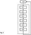
- Figure 2 shows a method flow for using the encoder structure 40 eg. as shown in
- Figure 1 for finding back a previously measure spot after tip change or angle change.
- This method requires a displacement encoder for encoding a displacement of said probe tip in one or more directions that the substrate holder moves relative to the sample tip, so that its position is known through a separate set of displacement encoders or sensors.
- a first step 101 after a scanning action 100 with a probe tip in a specific setting or orientation, the scan is finished at a scanning position of the probe tip relative to the substrate. In this position, it is aimed that the probe tip is changed in orientation or even replaced.
- the probe head is moved to the fiducial pattern (e.g. element 40 of Figure 1 ) to scan a first fiducial mark in the grid of fiducial marks at a first encoder position value.
- This first fiducial mark thus codes a first absolute position of the probe tip.
- the probe tip is changed, that is, the orientation of the probe tip may be changed or the probe tip may be interchanged; so that the tip position is altered relative to the probe head 17.
- the probe head is again positioned relative to the fiducial pattern, with the probe head at a first encoder position value.
- a second fiducial mark is scanned in the grid of fiducial marks while holding the probe head at the first encoder position value.
- This second fiducial mark codes a second absolute position of the probe tip. The difference between the first and second absolute positions is provided to the displacement encoder.
- the probe head is moved over a second encoder position value that is the first encoder position value, corrected by the distance of the second fiducial mark relative to the first fiducial mark.
- the method flow ends by resuming the scanning action 100 at the exact position where the probe tip initially finished scanning.
- Figure 3 shows a method where a single scannable structure 15a on substrate 15 is scanned under different angles.
- the structure 15a can be analyzed in three dimensions.
- the probe tip needs to be rotated to various angles ⁇ , e.g. a right angle of e.g. 2-45 degrees relative to the normal of the substrate; a top (flat) angle coinciding with the normal; and a left angle of 2-45 degrees relative to the normal of the substrate 15.
- ⁇ e.g. a right angle of e.g. 2-45 degrees relative to the normal of the substrate
- a top (flat) angle coinciding with the normal and a left angle of 2-45 degrees relative to the normal of the substrate 15.
- the probe tip 18 is moved to the fiducial pattern, where probe tip rotation is carried out.
- the probe tip may not exactly coincide with the end-point of the original probe tip position. It can be shifted in a lateral way, and by scanning the fiducial pattern, the lateral placement can be measured and compensated for when moving the tip
- Figure 4 shows an illustrative example of an absolute encoder structure 300, that may be a per se known QR coding mechanism for coding an X and Y coordinate in the QR code.
- the structure forms a grid 310 of fiducial marks 301, each coded with an X and Y code 302.
- X-coding and Y-coding 12 bits can be available, so that 2 ⁇ 12 points can be coded in both X- and Y- directions.
- the code size may be e.g. 5x5 blocks, and the coding may be provided in a patterning of diamond, silicon etc.
- the blocks may be provided with an additional orientation mark; e.g. a dot in one of the corner angles of the marks 301; so that it is clear how to interpret the least significant bit.
- the grid spacing may e.g. be 500 nm; where sub-pitch navigation accuracy can be achieved by determining where the center of the QR-code is situated within an AFM scan of the code.
- the top-left most QR-bit is the least significant bit for X
- the QR-bit immediately to the right of the center is the least significant bit of Y.
- the coded patterns 302 signify the corresponding bits.
- the fiducial mark 300 may not be a visual mark, but may simply be scannable by using the material properties that can be detected by the AFM probe head. It may be completely buried under a non-transparant capping layer.
- the mark 300 may be combined with a visual mark that may partly overlap the fiducial mark, and that may be suitable for (initial) alignment purposes.
- a visual mark may be provided by reflective material, for example aluminum stripes that are coated on the fiducial, in a layer thickness e.g. below 50 nm (e.g. 30 nm).
- the reflective material may be covered by a transparant material, wherein the QR code is provided; for example with a common origin with the visual mark.
- the transparent material may be first flattened by CMP polishing.
- the fiducial pattern may be provided with additional functionality; such as high aspect ratio test structures that may be used for calibration and characterization.
- additional functionality such as high aspect ratio test structures that may be used for calibration and characterization.
Abstract
The invention is directed at a method of performing scanning probe microscopy on a substrate surface using a scanning probe microscopy system. A probe tip and substrate surface are moved relative to each other in one or more directions parallel to the scanning plane to position the probe tip to a scanning position on the substrate surface with the probe tip; a displacement is measured by an encoder of said probe tip in said one or more directions; and a fiducial pattern is provided fixed relative to the substrate surface, said fiducial pattern having a scannable structure that is scannable by said probe tip and said structure forming a grid of fiducial marks in said one or more dimensions; said grid dimensioned to allow for measuring placement deviations of the probe tip relative to the probe head by identifying one or more fiducial marks in the fiducial pattern.
Description
- The present invention is directed at a method of performing scanning probe microscopy on a substrate surface using a scanning probe microscopy system, the system including at least one probe head, the probe head comprising a probe tip arranged on a cantilever and a tip position detector for determining a position of the probe tip along a z-direction transverse to an scanning plane, the method comprising positioning the at least one probe head relative to the substrate surface.
- The invention is further directed at a scanning probe microscopy system for performing microscopy on a substrate surface, the system including at least one probe head, the probe head comprising a probe tip arranged on a cantilever and a tip position detector for determining a position of the probe tip along a z-direction transverse to an scanning plane, wherein the system comprises a positioning structure for positioning the at least one probe head relative to the substrate surface.
- Scanning probe microscopy (SPM) devices, such as atomic force microscopy (AFM) devices, are for example applied in the semiconductor industry for scanning of semiconductor topologies on a surface. Other uses of this technology are found in biomedical industry, nanotechnology, and scientific applications. In particular, AFM may be used for critical dimension metrology (CD-metrology), particle scanning, stress- and roughness measurements. AFM microscopy allows visualization of surfaces at very high accuracy, enabling visualization of surface elements at sub-nanometer resolution.
- As a result of the high accuracy, conventional and available SPM devices are to be controlled precisely, and contain accurate and sensitive measuring equipment, as well as positioning and scanning equipment arranged for supporting the very high (e.g. nanometer) resolution. Correct calibration of the device parts and the use of a high resolution positioning feedback system enable the SPM device to provide the required accuracy. In an AFM the exact position of the tip attached to an AFM cantilever may shift a bit after a new cantilever has been loaded. In addition to this, a probe tip may be shifted when measuring with different tilt angles of the cantilever. Such an angle change may shift the tip a bit as well. This makes navigation to a specific structure on a sample, or finding it back difficult. The invention aims to determine the exact position of the tip with respect to the measurement systems coordinate system. This way, previously measured structures can be found back exactly even after tip exchange or angle change.
- It is an object of the present invention to provide a method of performing scanning probe microscopy that enables to be applied to large substrate surfaces without trade-off in terms of accuracy.
- To this end, there is provided herewith a method of performing scanning probe microscopy on a substrate surface using a scanning probe microscopy system, the system including at least one probe head, the probe head comprising a probe tip arranged on a cantilever and a tip position detector for determining a position of the probe tip along a z-direction transverse to an scanning plane, the method comprising: moving the probe tip and the substrate surface relative to each other in one or more directions parallel to the scanning plane to position the probe tip to a scanning position on the substrate surface with the probe tip;
measuring by a displacement encoder a displacement of said probe tip in said one or more directions; and
providing a fiducial pattern fixed relative to the substrate surface, said fiducial pattern having a scannable structure that is scannable by said probe tip and said structure forming a grid of fiducial marks in said one or more dimensions; said grid dimensioned to allow for measuring placement deviations of the probe tip relative to the probe head by identifying one or more fiducial marks in the fiducial pattern.
The fiducial pattern provides an absolute encoding of the substrate, in particular, relative to a substrate stage. This absolute encoder can be scanned by the probe tip itself. The resulting image is decoded so that position coordinates can be extracted from this. By integrating such an encoder with the substrate holder it is usable for alignment and position calibration purposes.
The probe tip may be moved by a positioning structure that is for example a positioning arm or an extendible arm which enables to move the probe head (or multiple probe heads simultaneously or consecutively) relative to the substrate surface towards desired landing position.
In accordance with a further embodiment, the displacement encoder measures a distance of the probe tip relative to at least one of a group comprising: a surface of a metrology frame, a surface that is statically connected to a metrology frame, and/or a two-dimensional optical encoder surface. In accordance with a preferred embodiment of the present invention, the displacement encoder is a two-dimensional optical encoder that is fixed to a metrology frame of the microscopy system. The two-dimensional optical encoder is designed for being absolutely static relatively to the metrology frame of the microscopy system. Moreover, the two-dimensional optical encoder is accurately calibrated such that it provides a highly reliable reference frame that can be used during scanning of the substrate surface. The two-dimensional optical encoder may comprise single encoder element, or may be formed of a plurality of encoder elements that are arranged contiguously such as to span a larger surface.
An optical encoder may comprise an optical grating that cooperates with an encoder device on the (at least one) probe. The encoder enables to determine the exact position of the probe head based on the regular structure of the grating. Such a grating surface is usually a highly sensitive surface, and any irregularities, such as even the smallest scratches or contaminations, may cause the grating surface to be no longer usable. For example, the encoder uses the regular structure of the grating as a reference, by counting the grating structures that have passed during movement of the encoder starting from a specific reference. Any irregularity may disrupt such counting, thereby destroying the accuracy of the reference. - In accordance with a further embodiment of the present invention, the step of moving the probe tip and the substrate surface relative to each other is performed by the probe head comprising a 'short stroke' actuator for moving the cantilever relative to the probe head in a direction parallel to the scanning plane for performing the scanning of the substrate surface. An actuator of this type only requires a very small stroke for spanning only the surface of the image to be made. Sufficiently accurate actuator systems are available for use in a method in accordance with this embodiment.
- In accordance with a further aspect of the present invention, there is provided a scanning probe microscopy system for performing scanning probe microscopy on a substrate surface using a scanning probe microscopy system, the system including:
- at least one probe head, the probe head comprising a probe tip arranged on a cantilever and a tip position detector for determining a position of the probe tip along a z-direction transverse to an scanning plane,
- an actuator for moving the probe tip and the substrate surface relative to each other in one or more directions parallel to the scanning plane to position the probe tip to a scanning position on the substrate surface with the probe tip;
- a displacement encoder form measuring a displacement of said probe tip in said one or more directions; and
- a fiducial pattern fixed relative to the substrate surface, said fiducial pattern having a scannable structure that is scannable by said probe tip and said structure forming a grid of fiducial marks in said one or more dimensions; said grid dimensioned to allow for measuring placement deviations of the probe tip relative to the probe head by identifying one or more fiducial marks in the fiducial pattern. Specific embodiments of such a scanning probe microscopy system are described herein, and are referred to in the enclosed claims.
- The invention will further be elucidated by description of some specific embodiments thereof, making reference to the attached drawings. The detailed description provides examples of possible implementations of the invention, but is not to be regarded as describing the only embodiments falling under the scope. The scope of the invention is defined in the claims, and the description is to be regarded as illustrative without being restrictive on the invention. In the drawings:
-
Figure 1 schematically illustrates a scanning probe microscopy system in accordance with the present invention, wherein the method of the present invention may be applied; -
Figure 2 shows a method flow for using the encoder structure; -
Figure 3 shows a method where a single scannable structure; -
Figure 4 (a and b) shows an illustrative example of an absolute encoder structure. -
Figure 1 schematically illustrates a scanning probe microscopy (SPM)system 1 of the present invention. TheSPM system 1 is suitable for being used in combination with the method of performing scanning probe microscopy in accordance with the present invention. TheSPM system 1 comprises a metrology frame 3. The metrology frame provides a solid fixed base for the system. For obtaining the desired accuracy, the metrology frame is preferably kept free from any vibrations, and ideally also temperature changes within or in the environment of the metrology frame 3 are ruled out as much as possible. - A
substrate holder 5 for carrying asubstrate 15 such as a wafer, is connected to an XYsubstrate holder actuator 7 by means of asubstrate holder arm 6. Thesubstrate holder actuator 7 may be a system that allows to move thesubstrate holder 5, and therewith thesubstrate 15, in the X and Y directions, i.e. the directions parallel to thesubstrate 15. Infigure 1 , thesubstrate holder actuator 7 is illustrated as a single actuator element. Although the skilled person may appreciate that the substrate holder actuator may be implemented in a number of different manners, allowing the X and Y movements to be performed by a single actuator; other manners of implementing the substrate holder actuator functionality may comprise two (or more) actuators. For example, a separate X- and Y- actuator may be provided; also, for providing actuation in an X-direction a long stroke actuator may cooperate with a short stroke actuator in well known fashion. Also, thesubstrate holder 5 may be fixed relative to the metrology frame 3; and all movements are provided by moving the probe head carrier 24 in a long stroke and theprobe tip 18 in a short stroke. - Back to
figure 1 , thesubstrate 15 comprises asubstrate surface 16 that requires to be scanned by the scanningprobe microscopy system 1. The scanningprobe microscopy system 1 may comprise one or more probe heads 17. The probe heads 17 may be placed at various locations relative to thesubstrate surface 16 using a positioning structure. The positioning structure comprises a positioning actuator 10 and an extendible arm 11. The extendible arm 11 comprises an engagement element 25 that can be used for engaging with aprobe head 17 for placement thereof relative to the substrate surface in a long stroke. - The probe heads 17 comprise, to this end, a probe head carrier 24 that cooperates with the engagement element 25. The probe head carrier 24 comprises the
cantilever actuator 14 to which the probe comprising thecantilever 19 and theprobe tip 18 are attached. A short stroke actuator (not shown) may be provided on the probe head carrier 24 to move thecantilever 19 andprobe tip 18 in a short stroke relative to the probe head carrier 24 in a direction parallel to the scanning plane for performing the scanning of the substrate surface. Thecantilever actuator 14 allows actuation of the probe in the Z direction, i.e. the direction perpendicular tosubstrate surface 16, preferably by means of the vibration of theprobe tip 18 in the Z direction. During scanning, by vibrating the probe tip and bringing the probe tip very close to thesubstrate surface 16, thesubstrate surface 16 can be scanned and any nanostructures present on thesubstrate surface 16 will influence the deflection of the probe tip. This probe tip deflection is measured using a tip position detector 21 comprising an interferometer. - In accordance with a method of the present invention, during scanning of the
substrate surface 16 theprobe head 17 is placed on a static carrier surface. Infigure 1 , this is achieved by placing the probe head carrier 24 with landing feet 27 onencoder 12. Theencoder 12 may be provided, by a highly sensitive optical grating, which is accurately calibrated such as to provide a reference structure that is usable for accurately determining the exact position and orientation of theprobe head 17 on the metrology frame 3. Alternatively, but not limited thereto, encoders may be provided in extendible arm 11 and/orsubstrate holder arms 6. By having this information, also the exact position of theprobe tip 19 with respect to the metrology frame is known. Theencoder 12, for this reason, is highly sensitive and prone to any scratching or contamination. To determine the exact position on the metrology frame 3, a counting may be performed on the regular structure of the grating periodicity of theencoder 12. Instead of or in addition to counting grating structures, the encoder surface may comprise other references that may be interpreted for determining an exact position. As may be appreciated, a scratch on the surface may disrupt the interpretation of the positioning reference, and thereby introduces an inaccuracy in the reference system. Prior to scanning of thesubstrate surface 16 using theprobe tip 18 of each of the probe heads 17, the probe heads are placed onto theencoder 12 by means of the extendible arm 11 and the positioning actuator 10. - In
figure 1 , thesubstrate holder 5 is illustrated in the lowered position: in the position wherein the scanning of thesubstrate surface 16 by theprobe tips 18 may take place. However during placement of the probe heads 17 on theencoder surface 12, thesubstrate holder 5 will be moved in an upward position such as to allow the placement of theheads 17 using the extendible arm 11. - Once the lowering of the
substrate holder 5 has been performed accurately, thesubstrate holder 5 is moved by scanningarm 6 in a scanning motion relative to encoder surface (and thereby theprobe tips 18 of the probe heads 17), to perform the scanning of thesubstrate surface 16. Accurate control of all movements performed by theactuators 7, and 10 will be controlled bycontroller 32 of the scanning probemicroscopy control system 30. Thecontrol system 30 further comprises amemory 35 and acommunications module 36 both connected to thecontroller 32 in a functional manner. Data obtained using the tip position detectors 21 of eachprobe head 17 is communicated to thecommunications module 36 of thecontrol system 30. This measurement data is stored inmemory 35, or may be forwarded onto a communications network for further processing remotely. Communication between thecommunications module 36 and each of the tip position detectors may comprise a wireline connection (not shown) or a wireless data communication connection. As will be appreciated, for sending the data wirelessly, theprobe head 17 may further comprise a wireless data communication module installed onboard. According to an aspect of the invention 40 ascannable encoder structure 40 is fixed relative to the substrate surface and dimensioned to allow for measuring placement deviations of theprobe tip 18 relative to theprobe head 17. As will be further elucidated with reference toFigure 3 , the scannable structure preferably forms a fiducial pattern of a grid of fiducial marks in said one or more dimensions; said grid dimensioned to allow for measuring placement deviations of the probe tip relative to theprobe head 17 by identifying one or more fiducial marks in the fiducial pattern. Preferably, the scannable structure is scannable by said probe tip and said structure forming, but also other scanning means, such as a laser may be used, that is e.g. arranged for scanning a fiducial mark and measuring the probe tip X and Y coordinate. The resulting image is decoded so that position coordinates can be extracted from this. When scannable by theprobe tip 18, several material properties may be used for obtaining a coded scanning signal, e.g. a coding provided by provided by varying a local stiffness, magnetic or material type property. Other properties can also be used, e.g. topography, surface potential, hardness, material type. While thescannable structure 40 is shown fixed to thesubstrate holder 5; it may also integral part of the substrate, e.g. it may be provided as a scannable pattern in silicon. It may also be a separate (silicon) substrate attached to thesubstrate holder 5. -
Figure 2 shows a method flow for using theencoder structure 40 eg. as shown in -
Figure 1 , for finding back a previously measure spot after tip change or angle change. - This method requires a displacement encoder for encoding a displacement of said probe tip in one or more directions that the substrate holder moves relative to the sample tip, so that its position is known through a separate set of displacement encoders or sensors. In a
first step 101, after ascanning action 100 with a probe tip in a specific setting or orientation, the scan is finished at a scanning position of the probe tip relative to the substrate. In this position, it is aimed that the probe tip is changed in orientation or even replaced. To allow for this, in asecond step 102 the probe head is moved to the fiducial pattern (e.g. element 40 ofFigure 1 ) to scan a first fiducial mark in the grid of fiducial marks at a first encoder position value. This first fiducial mark thus codes a first absolute position of the probe tip. Instep 103 the probe tip is changed, that is, the orientation of the probe tip may be changed or the probe tip may be interchanged; so that the tip position is altered relative to theprobe head 17. Instep 104, after changing the tip; the probe head is again positioned relative to the fiducial pattern, with the probe head at a first encoder position value. In step 105 a second fiducial mark is scanned in the grid of fiducial marks while holding the probe head at the first encoder position value. This second fiducial mark codes a second absolute position of the probe tip. The difference between the first and second absolute positions is provided to the displacement encoder. In astep 106 the probe head is moved over a second encoder position value that is the first encoder position value, corrected by the distance of the second fiducial mark relative to the first fiducial mark. - The method flow ends by resuming the
scanning action 100 at the exact position where the probe tip initially finished scanning. -
Figure 3 shows a method where a singlescannable structure 15a onsubstrate 15 is scanned under different angles. By scanning under different angles, thestructure 15a can be analyzed in three dimensions. However, in the execution, the probe tip needs to be rotated to various angles α, e.g. a right angle of e.g. 2-45 degrees relative to the normal of the substrate; a top (flat) angle coinciding with the normal; and a left angle of 2-45 degrees relative to the normal of thesubstrate 15. As the rotation of theprobe tip 18 cannot be executed in situ, theprobe tip 18 is moved to the fiducial pattern, where probe tip rotation is carried out. During rotation, the probe tip may not exactly coincide with the end-point of the original probe tip position. It can be shifted in a lateral way, and by scanning the fiducial pattern, the lateral placement can be measured and compensated for when moving the tip back to thestructure 15a. -
Figure 4 shows an illustrative example of anabsolute encoder structure 300, that may be a per se known QR coding mechanism for coding an X and Y coordinate in the QR code. - The structure forms a
grid 310 offiducial marks 301, each coded with an X andY code 302. For example for X-coding and Y-coding, 12 bits can be available, so that 2^12 points can be coded in both X- and Y- directions. The code size may be e.g. 5x5 blocks, and the coding may be provided in a patterning of diamond, silicon etc. The blocks may be provided with an additional orientation mark; e.g. a dot in one of the corner angles of themarks 301; so that it is clear how to interpret the least significant bit. - The grid spacing may e.g. be 500 nm; where sub-pitch navigation accuracy can be achieved by determining where the center of the QR-code is situated within an AFM scan of the code. E.g. In the example, the top-left most QR-bit is the least significant bit for X, the QR-bit immediately to the right of the center is the least significant bit of Y. More specifically,
Figure 4a shows a QR-code sample proposal for reproducible navigation, starting with (X,Y) = (0,0).Figure 4b shows the coding starting with (X,Y) = (1235,2346). The codedpatterns 302 signify the corresponding bits. Thefiducial mark 300 may not be a visual mark, but may simply be scannable by using the material properties that can be detected by the AFM probe head. It may be completely buried under a non-transparant capping layer. Themark 300 may be combined with a visual mark that may partly overlap the fiducial mark, and that may be suitable for (initial) alignment purposes. E.g. a visual mark may be provided by reflective material, for example aluminum stripes that are coated on the fiducial, in a layer thickness e.g. below 50 nm (e.g. 30 nm). The reflective material may be covered by a transparant material, wherein the QR code is provided; for example with a common origin with the visual mark. The transparent material may be first flattened by CMP polishing. The fiducial pattern may be provided with additional functionality; such as high aspect ratio test structures that may be used for calibration and characterization. The present invention has been described in terms of some specific embodiments thereof. It will be appreciated that the embodiments shown in the drawings and described herein are intended for illustrated purposes only and are not by any manner or means intended to be restrictive on the invention. The context of the invention discussed here is merely restricted by the scope of the appended claims.
Claims (20)
- A method of performing scanning probe microscopy on a substrate surface using a scanning probe microscopy system, the system including at least one probe head, the probe head comprising a probe tip arranged on a cantilever and a tip position detector for determining a position of the probe tip along a z-direction transverse to an scanning plane, the method comprising:- moving the probe tip and the substrate surface relative to each other in one or more directions parallel to the scanning plane to position the probe tip to a scanning position on the substrate surface with the probe tip;- measuring by a displacement encoder a displacement of said probe tip in said one or more directions; and- providing a scannable encoder structure fixed relative to the substrate surface and dimensioned to allow for measuring placement deviations of the probe tip relative to the probe head.
- A method according to claim 1 wherein the scannable structure forms a fiducial pattern of a grid of fiducial marks in said one or more dimensions; said grid dimensioned to allow for measuring placement deviations of the probe tip relative to the probe head by identifying one or more fiducial marks in the fiducial pattern.
- A method according to claim 1 or 2, wherein said scannable structure is scannable by said probe tip and said structure forming
- A method according to any of the previous claims, wherein the scannable structure is provided by varying a local stiffness, magnetic or material type property.
- A method according to any of the previous claims, wherein the scannable structure is fixed to the substrate holder.
- A method according to any of the previous claims, wherein the scannable structure is provided on a silicon substrate.
- A method according to any of the previous claims, wherein the scannable structure is provided as a QR code having coded X and Y coordinates.
- A method according to any of the previous claims, wherein the displacement encoder measures a distance of the probe tip relative to at least one of a group comprising: a surface of a metrology frame, a surface that is statically connected to a metrology frame, and/or a two-dimensional optical encoder surface.
- A method according to any of the previous claims, wherein said step of moving the probe tip and the substrate surface relative to each other is performed by the probe head comprising an actuator for moving the cantilever relative to the probe head in a direction parallel to the scanning plane for performing the scanning of the substrate surface.
- A method according to any of the previous claims, wherein the method comprises the steps of finishing a scan at the scanning position; moving the probe head to the fiducial pattern to scan a first fiducial mark in the grid of fiducial marks at a first encoder position value; changing the probe tip; scanning a second fiducial mark in the grid of fiducial marks; while holding the probe head at the first encoder position value; and resume the scanning position by moving the probe head over a second encoder position value that is the first encoder position value, corrected by the distance of the second fiducial mark relative to the first fiducial mark.
- A scanning probe microscopy system for performing scanning probe microscopy on a substrate surface using a scanning probe microscopy system, the system including:- a substrate holder for clamping the substrate;- at least one probe head, the probe head comprising a probe tip arranged on a cantilever and a tip position detector for determining a position of the probe tip along a z-direction transverse to an scanning plane defined by the substrate holder,- an actuator for moving the probe tip and the substrate holder relative to each other in one or more directions parallel to the scanning plane to position the probe tip to a scanning position on the substrate surface with the probe tip;- a displacement encoder form measuring a displacement of said probe tip in said one or more directions; and- a fiducial pattern fixed relative to the substrate holder, said fiducial pattern having a scannable structure that is scannable by said probe tip and said structure forming a grid of fiducial marks in said one or more dimensions; said grid dimensioned to allow for measuring placement deviations of the probe tip relative to the probe head by identifying one or more fiducial marks in the fiducial pattern.
- A system according to claim 11, wherein the scannable structure has a varying local stiffness, magnetic or material type property for detecting a coded fiducial mark.
- A system according to any of claim 11-12, wherein the scannable structure is provided on a silicon substrate.
- A system according to any of the previous claims 11-13, wherein the scannable structure is provided as a QR code having coded X and Y coordinates.
- A system according to any of the previous claims 11- 14, wherein the scannable structure comprises a visual mark that may partly overlap the scannable structure.
- A system according to any of the previous claims 11- 15, wherein the scannable structure comprises a orientation mark that allows to identify the orientation of the scannable structure relative to the probe tip.
- A system according to any of the previous claims 11- 16 wherein the displacement encoder measures a distance of the probe tip relative to at least one of a group comprising: a surface of a metrology frame, a surface that is statically connected to a metrology frame, and/or a two-dimensional optical encoder surface.
- A system according to any of the previous claims 11 -17, further comprising an actuator for moving the cantilever relative to the probe head in a direction parallel to the scanning plane for performing the scanning of the substrate surface.
- A scanning probe microscopy system according to any of the claims 11 - 18, further comprising an actuated substrate holder arranged for holding the substrate surface and for moving of the substrate surface in a direction parallel with the scanning plane for performing said scanning of the substrate surface with the probe tip.
- A system according to any of the previous claims 11 - 19, further comprising a controller arranged to carry out the steps of of finishing a scan at the scanning position; moving the probe head to the fiducial pattern to scan a first fiducial mark in the grid of fiducial marks at a first encoder position value; and, when the probe tip is changed; scanning a second fiducial mark in the grid of fiducial marks; while holding the probe head at the first encoder position value; and resume the scanning position by moving the probe head over a second encoder position value that is the first encoder position value, corrected by the distance of the second fiducial mark relative to the first fiducial mark.
Priority Applications (5)
| Application Number | Priority Date | Filing Date | Title |
|---|---|---|---|
| EP18185282.3A EP3599470A1 (en) | 2018-07-24 | 2018-07-24 | System and method of performing scanning probe microscopy on a substrate surface |
| KR1020217005290A KR20210035859A (en) | 2018-07-24 | 2019-07-24 | System and method for performing Scanning Probe Microscopy (SPM) on the substrate surface |
| EP19755992.5A EP3827269B1 (en) | 2018-07-24 | 2019-07-24 | System and method of performing scanning probe microscopy on a substrate surface |
| US17/261,494 US11320457B2 (en) | 2018-07-24 | 2019-07-24 | System and method of performing scanning probe microscopy on a substrate surface |
| PCT/NL2019/050482 WO2020022893A1 (en) | 2018-07-24 | 2019-07-24 | System and method of performing scanning probe microscopy on a substrate surface |
Applications Claiming Priority (1)
| Application Number | Priority Date | Filing Date | Title |
|---|---|---|---|
| EP18185282.3A EP3599470A1 (en) | 2018-07-24 | 2018-07-24 | System and method of performing scanning probe microscopy on a substrate surface |
Publications (1)
| Publication Number | Publication Date |
|---|---|
| EP3599470A1 true EP3599470A1 (en) | 2020-01-29 |
Family
ID=63041916
Family Applications (2)
| Application Number | Title | Priority Date | Filing Date |
|---|---|---|---|
| EP18185282.3A Withdrawn EP3599470A1 (en) | 2018-07-24 | 2018-07-24 | System and method of performing scanning probe microscopy on a substrate surface |
| EP19755992.5A Active EP3827269B1 (en) | 2018-07-24 | 2019-07-24 | System and method of performing scanning probe microscopy on a substrate surface |
Family Applications After (1)
| Application Number | Title | Priority Date | Filing Date |
|---|---|---|---|
| EP19755992.5A Active EP3827269B1 (en) | 2018-07-24 | 2019-07-24 | System and method of performing scanning probe microscopy on a substrate surface |
Country Status (4)
| Country | Link |
|---|---|
| US (1) | US11320457B2 (en) |
| EP (2) | EP3599470A1 (en) |
| KR (1) | KR20210035859A (en) |
| WO (1) | WO2020022893A1 (en) |
Cited By (4)
| Publication number | Priority date | Publication date | Assignee | Title |
|---|---|---|---|---|
| EP3901701A1 (en) * | 2020-04-23 | 2021-10-27 | Nederlandse Organisatie voor toegepast- natuurwetenschappelijk Onderzoek TNO | Determining alignment of layers in a layered product |
| WO2022060224A1 (en) * | 2020-09-17 | 2022-03-24 | Nearfield Instruments B.V. | Method, system and parts for enabling navigation in a scanning probe microscopy system |
| WO2022158980A1 (en) * | 2021-01-25 | 2022-07-28 | Nearfield Instruments B.V. | Positioning system and method |
| WO2022245208A1 (en) * | 2021-05-19 | 2022-11-24 | Nearfield Instruments B.V. | System for performing atomic force microscopy, including a grid plate qualification tool |
Families Citing this family (1)
| Publication number | Priority date | Publication date | Assignee | Title |
|---|---|---|---|---|
| CN114088979A (en) * | 2021-12-20 | 2022-02-25 | 百及纳米科技(上海)有限公司 | Probe calibration method, surface measurement method, and probe control apparatus |
Citations (3)
| Publication number | Priority date | Publication date | Assignee | Title |
|---|---|---|---|---|
| US6178653B1 (en) * | 1998-11-20 | 2001-01-30 | Lucent Technologies Inc. | Probe tip locator |
| US20030185967A1 (en) * | 2002-03-27 | 2003-10-02 | Eby Raymond K. | Method and apparatus for aligning patterns on a substrate |
| EP3258275A1 (en) * | 2016-06-17 | 2017-12-20 | Nederlandse Organisatie voor toegepast- natuurwetenschappelijk onderzoek TNO | Method of determining an overlay error, method for manufacturing a multilayer semiconductor device, atomic force microscopy device, lithographic system and semiconductor device |
Family Cites Families (3)
| Publication number | Priority date | Publication date | Assignee | Title |
|---|---|---|---|---|
| US20100175155A1 (en) * | 2009-01-06 | 2010-07-08 | President And Fellows Of Harvard College | Measurement and Mapping of Molecular Stretching and Rupture Forces |
| US10697998B2 (en) * | 2015-10-23 | 2020-06-30 | Nederlandse Organisatie Voor Toegepast-Natuurwetenschappelijk Onderzoek Tno | Method of performing surface measurements on a surface of a sample, and scanning probe microscopy system therefore |
| US10139429B2 (en) * | 2017-03-24 | 2018-11-27 | Fei Company | Method for calibrating and imaging using multi-tip scanning probe microscope |
-
2018
- 2018-07-24 EP EP18185282.3A patent/EP3599470A1/en not_active Withdrawn
-
2019
- 2019-07-24 EP EP19755992.5A patent/EP3827269B1/en active Active
- 2019-07-24 WO PCT/NL2019/050482 patent/WO2020022893A1/en unknown
- 2019-07-24 US US17/261,494 patent/US11320457B2/en active Active
- 2019-07-24 KR KR1020217005290A patent/KR20210035859A/en unknown
Patent Citations (3)
| Publication number | Priority date | Publication date | Assignee | Title |
|---|---|---|---|---|
| US6178653B1 (en) * | 1998-11-20 | 2001-01-30 | Lucent Technologies Inc. | Probe tip locator |
| US20030185967A1 (en) * | 2002-03-27 | 2003-10-02 | Eby Raymond K. | Method and apparatus for aligning patterns on a substrate |
| EP3258275A1 (en) * | 2016-06-17 | 2017-12-20 | Nederlandse Organisatie voor toegepast- natuurwetenschappelijk onderzoek TNO | Method of determining an overlay error, method for manufacturing a multilayer semiconductor device, atomic force microscopy device, lithographic system and semiconductor device |
Cited By (7)
| Publication number | Priority date | Publication date | Assignee | Title |
|---|---|---|---|---|
| EP3901701A1 (en) * | 2020-04-23 | 2021-10-27 | Nederlandse Organisatie voor toegepast- natuurwetenschappelijk Onderzoek TNO | Determining alignment of layers in a layered product |
| WO2021215915A1 (en) | 2020-04-23 | 2021-10-28 | Nederlandse Organisatie Voor Toegepast- Natuurwetenschappelijk Onderzoek Tno | Determining alignment of layers in a layered product |
| WO2022060224A1 (en) * | 2020-09-17 | 2022-03-24 | Nearfield Instruments B.V. | Method, system and parts for enabling navigation in a scanning probe microscopy system |
| NL2026497B1 (en) * | 2020-09-17 | 2022-05-23 | Nearfield Instr B V | Method, system and parts for enabling navigation in a scanning probe microscopy system. |
| WO2022158980A1 (en) * | 2021-01-25 | 2022-07-28 | Nearfield Instruments B.V. | Positioning system and method |
| WO2022245208A1 (en) * | 2021-05-19 | 2022-11-24 | Nearfield Instruments B.V. | System for performing atomic force microscopy, including a grid plate qualification tool |
| NL2028248B1 (en) * | 2021-05-19 | 2022-12-06 | Nearfield Instr B V | Grid Plate Qualification Tool Concept |
Also Published As
| Publication number | Publication date |
|---|---|
| EP3827269A1 (en) | 2021-06-02 |
| WO2020022893A1 (en) | 2020-01-30 |
| KR20210035859A (en) | 2021-04-01 |
| US11320457B2 (en) | 2022-05-03 |
| EP3827269B1 (en) | 2023-09-20 |
| US20210318353A1 (en) | 2021-10-14 |
Similar Documents
| Publication | Publication Date | Title |
|---|---|---|
| EP3827269B1 (en) | System and method of performing scanning probe microscopy on a substrate surface | |
| US7946029B2 (en) | Apparatus for aligning a first article relative to a second article | |
| CN105408991A (en) | Substrate holding method, substrate holding apparatus, exposure method, and exposure apparatus | |
| CN108225213A (en) | The non-contact dimensionality reduction error separate detection method of free form surface and device | |
| US10712674B2 (en) | Method of determining an overlay error, manufacturing method and system for manufacturing of a multilayer semiconductor device, and semiconductor device manufactured thereby | |
| US20090147237A1 (en) | Spatial Phase Feature Location | |
| EP3164720B1 (en) | System and method of performing scanning probe microscopy on a substrate surface | |
| JP4050459B2 (en) | Device for detecting the position of two objects | |
| EP2867682B1 (en) | High throughput scanning probe microscopy device | |
| CN102507985A (en) | Incline measuring method for STM (Scanning Tunneling Microscope) with vertical side wall micro structure | |
| KR101854177B1 (en) | Processing implement position alignment device for component and method thereof | |
| JP2023011855A (en) | Mark field, and method and device for specifying position | |
| NL2028082B1 (en) | Fiducial marker design, fiducial marker, scanning probe microscopy device and method of calibrating a position of a probe tip. | |
| CN101868140B (en) | Device suitable for placing a component on a substrate, as well as such a method | |
| US20050010310A1 (en) | Method of alignment for precision tools. | |
| JP2006349537A (en) | Method and apparatus for measuring pattern dimensions | |
| Wertjanz et al. | Range extension for large-scale robotic precision 3D measurements in vibration-prone environments | |
| US10488433B2 (en) | Positioning arm for and method of placing a scan head on a support surface | |
| CN116057476A (en) | Apparatus and method for determining alignment masks on a sample stage displaceable along and rotatable with respect to at least one axis | |
| CN113853671A (en) | System and method for transferring a device or pattern to a substrate | |
| JP2008076738A (en) | Exposure apparatus | |
| Ritter et al. | A 3D-Calibration Method for the Quantitative SPM Measurement of Hardness Intenders | |
| JPH06201372A (en) | Method for measuring probe position of probe microscope |
Legal Events
| Date | Code | Title | Description |
|---|---|---|---|
| PUAI | Public reference made under article 153(3) epc to a published international application that has entered the european phase |
Free format text: ORIGINAL CODE: 0009012 |
|
| AK | Designated contracting states |
Kind code of ref document: A1 Designated state(s): AL AT BE BG CH CY CZ DE DK EE ES FI FR GB GR HR HU IE IS IT LI LT LU LV MC MK MT NL NO PL PT RO RS SE SI SK SM TR |
|
| AX | Request for extension of the european patent |
Extension state: BA ME |
|
| STAA | Information on the status of an ep patent application or granted ep patent |
Free format text: STATUS: THE APPLICATION IS DEEMED TO BE WITHDRAWN |
|
| 18D | Application deemed to be withdrawn |
Effective date: 20200730 |