EP3598568B1 - Abstimmbare sonde für hochleistungsfähige kreuzgekoppelte hf-filter - Google Patents
Abstimmbare sonde für hochleistungsfähige kreuzgekoppelte hf-filter Download PDFInfo
- Publication number
- EP3598568B1 EP3598568B1 EP19183289.8A EP19183289A EP3598568B1 EP 3598568 B1 EP3598568 B1 EP 3598568B1 EP 19183289 A EP19183289 A EP 19183289A EP 3598568 B1 EP3598568 B1 EP 3598568B1
- Authority
- EP
- European Patent Office
- Prior art keywords
- resonator
- wire
- resonators
- tunable
- tunable probe
- Prior art date
- Legal status (The legal status is an assumption and is not a legal conclusion. Google has not performed a legal analysis and makes no representation as to the accuracy of the status listed.)
- Active
Links
Images


Classifications
-
- H—ELECTRICITY
- H01—ELECTRIC ELEMENTS
- H01P—WAVEGUIDES; RESONATORS, LINES, OR OTHER DEVICES OF THE WAVEGUIDE TYPE
- H01P1/00—Auxiliary devices
- H01P1/20—Frequency-selective devices, e.g. filters
- H01P1/207—Hollow waveguide filters
- H01P1/208—Cascaded cavities; Cascaded resonators inside a hollow waveguide structure
-
- H—ELECTRICITY
- H01—ELECTRIC ELEMENTS
- H01P—WAVEGUIDES; RESONATORS, LINES, OR OTHER DEVICES OF THE WAVEGUIDE TYPE
- H01P1/00—Auxiliary devices
- H01P1/20—Frequency-selective devices, e.g. filters
- H01P1/201—Filters for transverse electromagnetic waves
- H01P1/205—Comb or interdigital filters; Cascaded coaxial cavities
- H01P1/2053—Comb or interdigital filters; Cascaded coaxial cavities the coaxial cavity resonators being disposed parall to each other
-
- H—ELECTRICITY
- H01—ELECTRIC ELEMENTS
- H01P—WAVEGUIDES; RESONATORS, LINES, OR OTHER DEVICES OF THE WAVEGUIDE TYPE
- H01P1/00—Auxiliary devices
- H01P1/20—Frequency-selective devices, e.g. filters
- H01P1/207—Hollow waveguide filters
- H01P1/208—Cascaded cavities; Cascaded resonators inside a hollow waveguide structure
- H01P1/2084—Cascaded cavities; Cascaded resonators inside a hollow waveguide structure with dielectric resonators
-
- H—ELECTRICITY
- H01—ELECTRIC ELEMENTS
- H01P—WAVEGUIDES; RESONATORS, LINES, OR OTHER DEVICES OF THE WAVEGUIDE TYPE
- H01P1/00—Auxiliary devices
- H01P1/20—Frequency-selective devices, e.g. filters
- H01P1/2002—Dielectric waveguide filters
-
- H—ELECTRICITY
- H01—ELECTRIC ELEMENTS
- H01P—WAVEGUIDES; RESONATORS, LINES, OR OTHER DEVICES OF THE WAVEGUIDE TYPE
- H01P7/00—Resonators of the waveguide type
- H01P7/04—Coaxial resonators
-
- H—ELECTRICITY
- H01—ELECTRIC ELEMENTS
- H01P—WAVEGUIDES; RESONATORS, LINES, OR OTHER DEVICES OF THE WAVEGUIDE TYPE
- H01P7/00—Resonators of the waveguide type
- H01P7/10—Dielectric resonators
-
- H—ELECTRICITY
- H03—ELECTRONIC CIRCUITRY
- H03H—IMPEDANCE NETWORKS, e.g. RESONANT CIRCUITS; RESONATORS
- H03H7/00—Multiple-port networks comprising only passive electrical elements as network components
- H03H7/01—Frequency selective two-port networks
- H03H7/0138—Electrical filters or coupling circuits
-
- H—ELECTRICITY
- H03—ELECTRONIC CIRCUITRY
- H03H—IMPEDANCE NETWORKS, e.g. RESONANT CIRCUITS; RESONATORS
- H03H7/00—Multiple-port networks comprising only passive electrical elements as network components
- H03H7/01—Frequency selective two-port networks
- H03H7/0153—Electrical filters; Controlling thereof
- H03H7/0161—Bandpass filters
- H03H7/0169—Intermediate frequency filters
Definitions
- the present disclosure generally relates to tunable probes, such as band-pass filters, for use in radio frequency (RF) applications.
- RF radio frequency
- Communications systems utilize various filters to allow or inhibit signals selectively with varying frequency. Typically, noise or unwanted frequencies are inhibited or blocked and the desired signal is allowed to pass through for processing. Some band pass filters are constructed using elements that resonate.
- satellite communication systems utilize microwave communications frequencies that range from 1-30 Gigahertz (GHz). Additional goals of many satellite-based communication system components are to reduce weight in order to reduce costs associated with launching a satellite into orbit and to utilize approved components for space technology. Developing communication materials that utilize approved materials, have a reduced weight, and provide the correct signal processing characteristics is a challenge.
- GHz gigahertz
- Patent document EP 0 930 666 A1 in accordance with its abstract, describes a dielectric filter including a shielding cavity frame having electric conductivity, a dielectric having electrodes formed on two opposing faces and disposed in the shielding cavity frame, and external coupling means, wherein the external coupling means includes an electric probe at least a part of which is covered with a covering dielectric.
- Patent document DE 22 18 277 A1 in accordance with its abstract, describes at least three resonators, mounted in series in the wave propagation direction between parallel plates, form the microwave filter and are in the form of pins. Their inductive and capacitive coupling is determined by their spacing. At least one bypass coupling is provided between two resonators not immediately adjacent. The bypass coupling is so rated that the asymmetry of the filter pass characteristic is compensated. This asymmetry is produced by inductive coupling between not adjacent resonators. If at least four resonators are used, at least two capacitive additional couplings are provided between not adjacent resonators to make the design symmetric.
- Patent document CN 103 296 359 A in accordance with its abstract, describes a filter comprising a cavity with an inner cavity, an input end and an output end, wherein the input end and the output end are installed on the cavity, at least two resonant cavities are formed in the cavity, a harmonic oscillator is arranged in each resonant cavity, the input end and the output end of each resonant cavity are of a structure with wires in the middle and insulating material surrounding the wires, every two adjacent cavities are mutually connected through a metal piece electrically , and at least a part of the projection of the metal piece in the direction from the output ends of every two adjacent resonant cavities to the input ends of every two adjacent resonant cavities is located outside the projection of the wires in the same direction, wherein the wires are located at the output ends and the input ends of every two resonant adjacent cavities.
- Patent document EP 2 421 085 A1 states: a filter for radio frequency signals comprises a first cavity resonator, a second cavity resonator, an inner separating plate separating the first cavity resonator and the second cavity resonator and extending upwards from a base plate, a first capacitive coupling means penetrating the inner separating plate at a first height level with respect to the base plate and a second capacitive coupling means penetrating the inner separating plate at a second height level with respect to the base plate.
- Patent document CN 202 550 047 U states: a PCB cross coupling piece.
- the PCB cross coupling piece is applied in a passive cavity and is a PCB provided with a copper sheet layer in the middle.
- the PCB provided with the copper sheet layer in the middle is adopted to replace a prior art cross coupling rod.
- the PCB provided is shaped in one-time processing.
- Patent document EP 1 895 615 A1 discloses a coaxial resonator filter with a cross-couple between adjacent cavities, wherein the cross-couple allows extending the arms carrying the capacitive plates in a symmetric way for providing tuning flexibility.
- a tunable probe in one aspect of the present disclosure, includes a first resonator, a second resonator spaced from the first resonator, and a cross-couple extending from the first resonator to the second resonator.
- the cross-couple includes a first substrate and a second substrate disposed between the first and second resonators to create a capacitance between the first and second resonators.
- the cross-couple further includes a wire connecting the first and second substrates and a dielectric surrounding the wire.
- a cross-couple for a tunable probe in another aspect of the invention, includes a first substrate and a second substrate, the first and second substrates both having a first portion and a second portion.
- a wire connects the first portion of the first and second substrates and a dielectric surrounds the wire.
- the first portion is a metallic portion and the second portion is an alumina substrate portion.
- a method of tuning a tunable probe is provided.
- a cross-couple is disposed between a first resonator and a second resonator.
- the cross-couple includes a first substrate and a second substrate disposed between the first and second resonators to create a capacitance between the first and second resonators, a wire connecting each of the first and second substrates, and a dielectric surrounding the wire.
- the method further includes adjusting a position of the cross-couple along a lateral axis between the first and second resonators and bonding the cross-couple in place between the first and second resonators. Additional aspects are defined by the claims of this patent.
- FIG. 1 is an isometric view of a first tunable probe in accordance with an embodiment of the present disclosure.
- FIG. 1 depicts the tunable probe 100 that includes a tunable-probe inlet 110 and a tunable-probe outlet 112 connected to the housing 116.
- the tunable probe 100 may be connected into a communication system via the tunable probe inlet 110 and outlet 112 in order to provide filtering characteristics to the radio frequency (RF) signals in the communication system.
- the housing 116 includes a gap 119 between a first arm 122 and a second arm 124.
- the tunable probe 100 may also include various tunable screws 118 disposed about the housing between the resonators 114.
- the tunable probe 100 further includes a plurality of resonators 114.
- the positions of the resonators are indicated by a suffix after the resonator number (e.g., the '6' in '114-6' indicates a sixth resonator position).
- the tunable probe 100 includes twelve (12) resonators 114.
- a resonator 114 may be realized by a cylindrical-shaped cavity within the housing 116.
- a resonator 114 is included at a first resonator position 114-1 within the housing 116 adjacent to the tunable-probe inlet 110.
- the resonator positions increase incrementally in a counter-clockwise direction along the housing 116, starting at the tunable-probe inlet 110.
- the next resonator position after the first resonator position 114-1 is the second resonator position 114-2.
- the convention continues through to the twelfth (and final) resonator position 114-12 adjacent to the tunable-probe outlet 112.
- a tunable probe 100 includes a first resonator 114 spaced apart from the second resonator 114.
- the first resonator 114 may be at the fourth resonator position 114-4 and the second resonator 114 may be at the ninth resonator position 114-9, which is spaced apart and across from the first resonator 114.
- a cross-couple 120 extends from the first resonator 114 to the second resonator 114. The cross-couple 120 is discussed in more detail in conjunction with the discussion of FIG. 2 .
- the resonators 114 in a tunable probe are grouped in pairs.
- the tunable probe 100 includes six pairs of resonators 114. Each of the six pairs include two resonators 114 located opposite of each other.
- a first pair includes the resonators 114 located at the first resonator position 114-1 and the twelfth resonator position 114-12.
- the sixth pair includes the resonators 114 located at the sixth resonator position 114-6 and the seventh resonator position 114-7.
- one method of improving signal processing capabilities of a tunable probe is to increase the number of pairs of resonators 114 within the housing 116. However, this method results in excess material in a larger housing.
- Another method is to include a cross-couple between a pair of resonators, such as the cross-couple 120.
- a conductive wire may be able to provide sufficient capacitance to provide the desired signal processing characteristics.
- the capacitance of a just a conductive wire may not be sufficient to achieve the desired response.
- FIG. 2 is a detailed view of a cross-couple of the first tunable probe depicted in FIG. 1 , in accordance with an embodiment of the present disclosure.
- FIG. 2 depicts the view 200, which is a top-view of a portion of the tunable probe 100 and details aspects of the cross-couple 120.
- the cross-couple 120 includes a first substrate 202-1 in proximity to the first resonator 114 located at resonator position 114-4 and a second substrate 202-2 in proximity to the second resonator 114 located at resonator position 114-9.
- the cross-couple 120 is disposed between the first and second resonators 114 to create a capacitance between the first and second resonators 114.
- a wire 206 connects the first and second substrates 202-1, 202-2.
- a dielectric 208 surrounds the wire 206.
- the wire 206 is a silver wire, although certainly other conductive materials such as copper, gold, or the like may be used.
- the dielectric 208 also prevents the wire 206 from shorting against the housing 116.
- the first and second resonators 114 are disposed in the housing 116.
- a space between the first arm 122 and the second arm 124 defines a gap 119.
- the wire 206 extends across the gap 119 to define an exposed wire portion, and the dielectric 208 surrounds the exposed wire portion.
- the tunable probe 100 is configured to operate in either one or both of the X and L microwave communication/radio/frequency bands having a frequency range between 8-12 GHz and 1-2 GHz, respectively.
- the capacitance of a conductive wire alone utilized as a cross-couple between a pair of resonators 114 is insufficient to create the desired filtering performance of the tunable probe.
- the cross-couple 120 extending between two resonators 114, includes a first substrate 202-1 and a second substrate 202-2 connected via the wire 206.
- the first substrate 202-1 is located in proximity to the first resonator 114 at the fourth resonator position 114-4 and the second substrate 202-2 is located in proximity to the second resonator 114 at the ninth resonator position 114-9.
- the material of the first and second substrates 202-1, 202-2 are selected to have a material permittivity ( ⁇ r and also illustrated as Er) between 9.5 and 10.0.
- One such material may include alumina substrate.
- the first substrate 202-1 and the second substrate 202-2 may both include a first portion 216-1 and 216-2, respectively, and a second portion 218-1 and 218-2, respectively.
- the wire 206 connects the first portion 216-1 of the first substrate 202-1 with the first portion 216-2 of the second substrate 202-2.
- the second portion (218-1, 218-2) is oriented towards a respective resonator (114, 314) comprising the first resonator or the second resonator.
- the second portion 218-1 of the first substrate 202-1 is oriented towards (e.g., is located adjacent to or facing) the first resonator 114 on a side opposite of the first portion 216-1 as the wire 206.
- the second portion 218-2 of the second substrate 202-2 is oriented towards (e.g., is located adjacent to) the second resonator 114 on a side opposite of the first portion 216-2 as the wire 206.
- the material of the first portion 216-1, 216-2 is metallic (e.g., silver, gold) and the material of the second portion 218-1, 218-2 is selected based on a desired material permittivity (e.g., alumina substrate).
- the first portion 216-1, 216-2 of the first and second substrates 202-1, 202-2 may be rectangular and have a length and a width dimension. Further, the second portion 218-1, 218-2 of the first and second substrates 202-1, 202-2 may also be rectangular and have a length and a width dimension the same as the first portion 216-1, 216-2.
- the size (e.g., the cross-sectional area) of the first portion 216-1, 216-2 and the second portion 218-1, 218-2 may be selected based on desired filtering parameters of the tunable probe 100. In addition to rectangles, the sizes of the first portion 216-1, 216-2 and the second portion 218-1, 218-2 may be also be circular, oval, or the like.
- an inner surface of the first portion 216-1, 216-2 is affixed to the wire 206.
- Example methods of affixing to the first portions to the wire 206 include bonding with epoxy, soldering, and the like.
- An outer surface, opposite the inner surface, of the first portion 216-1, 216-2 is affixed to the second portion 218-1, 218-2.
- Example methods of affixing the first portions to the second portions include bonding with epoxy, folding edges of the first portion 216-1, 216-2 about the second portion to partially enclose and mechanically capture the second portion 218-1, 218-2, and the like.
- the substrates 202-1, 202-2 include the second portion 218-1, 218-2 affixed directly to the wire 206 without the first portion 216-1, 216-2.
- the tunable probe 100 is tunable at least in part by adjusting a location of the dielectric 208 along a lateral axis 220.
- the lateral axis 220 extends between the first and second resonators 114 and is parallel to a longitudinal axis of the wire 206.
- the dielectric 208 is fixed (e.g., bonded with epoxy) to the wire 206 at the determined, based on the desired tuning, location along the lateral axis 220 between the first and second resonators 114.
- the housing 116 may further include a recess in each arm 122, 124 along the lateral axis 220.
- the recesses are configured to receive a portion of the dielectric 208 to permit translation of the dielectric 208 along the lateral axis 220 to assist in tuning of the tunable probe 100.
- a portion of the dielectric 208 may also be bonded to the housing 116 at the recesses.
- FIG. 3 is an isometric view of a second tunable probe in accordance with an embodiment of the present disclosure.
- FIG. 3 depicts an isometric view of the tunable probe 300.
- the tunable probe 300 is similar to the tunable probe 100 discussed in conjunction with FIG. 1 . While the tunable probe 100 comprises a total of twelve resonators 114, with the cross-couple 120 extending between the resonators at the fourth resonator position 114-4 and the ninth resonator position 114-9, other configurations are likewise achievable.
- the tunable probe 300 includes eight resonators, with a cross-couple extending between the resonators at the second and seventh positions.
- the components of the tunable probe 300 are similar to like-numbered components of the tunable probe 100, with the tunable probe 300 including a tunable-probe inlet 310, a tunable probe outlet 312, a plurality of resonators 314, and a housing 316 having a first arm 322 and a second arm 324.
- the first and second arms 322, 324 define a gap 319.
- a cross-couple 320 is disposed between the first resonator 314 and a second resonator 314.
- a first difference is that the tunable probe 300 includes 8 resonators 314 (as compared to 12 resonators 114 of the tunable probe 100).
- a second difference is that the cross-couple 320 extends between the first resonator 314 located at the second resonator position 314-2 and the second resonator 314 located at the seventh resonator position 314-7 (as compared to the cross-couple 120 extending between resonators 114 at the fourth and ninth resonator positions of the tunable probe 100).
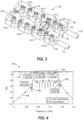
- FIG. 4 is a chart of signal processing characteristics of a tunable probe, in accordance with an embodiment of the present disclosure.
- FIG. 4 is a chart 400 that depicts the filtering characteristics of the tunable probe 100.
- the vertical axis depicts signal level, measured in decibels (dB).
- the horizontal axis depicts frequency of the communications signal, measured in GHz.
- the curve 402 depicts forward transmission and the curve 410 depicts forward reflection, as measured across the tunable-probe inlet 110 and the tunable-probe outlet 112 at each of the different frequencies.
- the tunable probe 100 acts as a band-pass filter centered around approximately 2 GHz. This is indicated by the band pass region 404 having a 0 dB measurement between 1.96 GHz and 2.2 GHz.
- a first notch 406 is located at a frequency just below the band pass region 404 (e.g., 1.92 GHz).
- a second notch 408 is located at a frequency just above the band pass region 404 (e.g., 2.25 GHz). Outside of the band pass region 404, the value of the forward transmission curve 402 drops off steeply.
- FIG. 5 depicts a cross-couple, in accordance with an embodiment of the present disclosure.
- FIG. 5 depicts a cross-couple, in accordance with an embodiment of the present disclosure.
- FIG. 5 depicts a cross-couple, in accordance with an embodiment of the present disclosure. In particular, FIG.
- the cross-couple 520 includes the first and second substrates 202-1, 202-2, the dielectric 208, and a wire 506.
- the first and second substrates 202-1, 202-2 each include the first portions 216-1, 216-2 that are near the wire 506 and the second portions 218-1, 218-2 that are opposite of the first portions 216-1, 216-2 and are configured to be oriented towards a resonator (e.g., 114, 314).
- the wire 506 is similar to the wire 206 and further includes bends 508-1, 508-2 and attachment portions 510-1, 510-2 on each end of the wire 506.
- an initially straight and unbent piece of wire is inserted through a bore hole of the dielectric 208.
- a forming tool is used to bend the wire to introduce the bends 508-1, 508-2 and attachment portions 510-1, 510-2 into the initially straight and unbent piece of wire.
- the wire may initially include one bend 508 and one attachment portion 510 on a first end of the wire, with the second end of the wire being straight and unbent. After the second end of the wire is inserted through a bore in the dielectric 208, the second end of the wire may be bent to introduce the second bend 508 and the second attachment portion 510.
- the first and second substrates 202-1, 202-2 are attached to the respective attachment portions 510-1, 510-2 on the respective ends of the wire 506.
- the attachment portions 510-1, 510-2 are essentially perpendicular to the first and second substrates 202-1, 202-2 and provide an increased surface area to attach the substrates 202-1, 202-2 to the wire 506.
- Example methods to attach the wire 506 to the substrates 202-1, 202-2 at the attachment portions 510-1, 510-2 include soldering and gold-epoxying the pieces together at a mating surface 512-1, 512-2.
- the cross-couple 520 may be inserted into the housing (e.g., 116) along a lateral axis between a pair of resonators (e.g., along the lateral axis 220).
- the wire 506 is bonded to the dielectric 208 at the determined location to tune the probe (e.g., adjust the slope of the notches at either end of the band-pass region).
- the tunable probe 100 is utilized in a satellite-based communication system as a band-pass filter, operating in either one of the X and L bands.
- one engineering objective is to manufacture the tunable probe out of materials approved for use in satellite communication systems.
- Another engineering objective is to reduce the overall weight and size of the tunable probe.
- a final engineering objective is to have the tunable probe permit communication frequencies of approximately X or L frequency band to pass through while attenuating frequencies outside of a band pass region.
- any other suitable tunable probe e.g., the tunable probe 300, a tunable probe with a different number of resonators or different location of the cross-couple
- any other suitable tunable probe e.g., the tunable probe 300, a tunable probe with a different number of resonators or different location of the cross-couple
- the tunable probe 100 includes components manufactured from an approved list of materials.
- the wire 206 is manufactured from silver
- the second portions 218-1, 218-2 of the respective substrates 202-1, 202-2 are manufactured from alumina substrate.
- the cross-couple 120 extends between the first resonator 114 located in the fourth resonator position 114-4 and the second resonator 114 located in the ninth resonator position 114-9.
- the alumina substrate in the cross-couple 120 provides sufficient capacitance between the first and second resonators 114 in order to provide the appropriate notches 406, 408 at either end of the band pass region 404.
- the tunable probe 100 is further able to be tuned, as described in conjunction with FIG. 6 .
- FIG. 6 is a method of tuning a tunable probe, in accordance with an embodiment of the present disclosure.
- FIG. 6 depicts the method 600 that includes disposing a cross-couple between resonators at block 602, adjusting the position of the cross-couple along the lateral axis at block 604, and bonding the cross-couple in place at block 606.
- the tunable probe 100 may be used in order to perform the method 600, although any of the other tunable probes and cross-couples disclosed herein may similarly be used to perform the method 600.
- the cross-couple 120 is disposed between the first and second resonators 114, such as between the resonators at the fourth 114-4 and ninth 114-9 resonator positions.
- the cross-couple 120 may be any cross-couple described herein, and includes a first and a second substrate 202-1, 202-2 connected by a wire 206, with a dielectric 208 surrounding the wire 206.
- a position of the cross-couple 120 is adjusted along the lateral axis 220 between the first and second resonators 114.
- the cross-couple 120 is bonded in place, at the adjusted position, between the first and second resonators 114.
- a tunable probe comprises: a first resonator; a second resonator spaced from the first resonator; and a cross-couple extending from the first resonator to the second resonator, the cross-couple comprising: a first substrate and a second substrate, the first and second substrates disposed between the first and second resonators to create a capacitance between the first and second resonators; a wire connecting the first and second substrates; and a dielectric surrounding the wire.
- a material permittivity (Er) of the first and second substrates is between 9.5 and 10.0.
- the first and second substrates comprise alumina substrate.
- the tunable probe is configured to operate in either one or both of the X and L frequency bands.
- the tunable probe is a band pass filter configured to pass a frequency of 2 GHz.
- the first and second substrates comprise both a metallic portion bonded to the wire and an alumina substrate portion facing a respective resonator comprising the first resonator or the second resonator.
- the first and second resonators are disposed in a housing defining a gap; the wire extends across the gap to define an exposed wire portion; and the dielectric surrounds the exposed wire portion.
- the wire comprises a silver wire.
- the tunable probe is tunable at least in part by adjusting a location of the dielectric along a lateral axis and bonding the dielectric to the wire between the first and second resonators.
- the tunable probe of the first example is tuned at least in part by selecting a size of the first and second substrates.
- the tunable probe of the first example comprises twelve resonators; the first resonator is at a fourth resonator position; and the second resonator is at a ninth resonator position, opposite of the fourth resonator position.
- the tunable probe comprises eight resonators; the first resonator is at a second resonator position; and the second resonator is at a seventh resonator position, opposite of the second resonator position.
- a cross-couple for a tunable probe comprising: a first substrate and a second substrate, the first and second substrates having both a first portion and a second portion; a wire connecting the first portion of the first and second substrates; and a dielectric surrounding the wire.
- the cross-couple of the second example is configured to be disposed between a first and second resonator to create a capacitance between the first and second resonators.
- the cross-couple is configured to tune the tunable probe at least in part by positioning the cross-couple along a lateral axis between the first and second resonators.
- the first and second substrates comprise alumina substrate having a material permittivity (Er) between 9.5 and 10.0.
- the second portion is oriented towards a respective resonator comprising the first resonator or the second resonator.
- the first and second substrates are bonded to the wire with epoxy.
- the dielectric is bonded to the wire with epoxy.
- a method of tuning a tunable probe comprising: disposing a cross-couple between a first resonator and a second resonator, the cross-couple comprising: a first substrate and a second substrate, the first and second substrates disposed between the first and second resonators to create a capacitance between the first and second resonators; a wire connecting each of the first and second substrates; and a dielectric surrounding the wire; adjusting a position of the cross-couple along a lateral axis between the first and second resonators; and bonding the cross-couple in place between the first and second resonators.
Landscapes
- Physics & Mathematics (AREA)
- Electromagnetism (AREA)
- Control Of Motors That Do Not Use Commutators (AREA)
Claims (15)
- Abstimmbare Sonde (100, 300), umfassend:einen ersten Resonator (114, 314);einen zweiten Resonator (114, 314), der von dem ersten Resonator (114, 314) beabstandet ist; undeine Kreuzkopplung (120, 320), die sich von dem ersten Resonator (114, 314) zu dem zweiten Resonator (114, 314) erstreckt, wobei die Kreuzkopplung (120, 320) umfasst:ein erstes Substrat (202-1) und ein zweites Substrat (202-2), wobei das erste und das zweite Substrat (202-1, 202-2) zwischen dem ersten und dem zweiten Resonator (114, 314) angeordnet sind, um eine Kapazität zwischen dem ersten und dem zweiten Resonator (114, 314) zu erzeugen;einen Draht (206), der das erste und das zweite Substrat (202-1, 202-2) verbindet; undein Dielektrikum (208), das den Draht (206) umgibt,wobei die abstimmbare Sonde (100, 300) mindestens teilweise dadurch abstimmbar ist, dass sie zum Einstellen einer Lage des Dielektrikums (208) entlang einer lateralen Achse (220), parallel zu einer Längsachse des Drahts (206), und Bonden des Dielektrikums (208) mit dem Draht (206) zwischen dem ersten und dem zweiten Resonator (114) konfiguriert ist.
- Abstimmbare Sonde (100, 300) nach Anspruch 1, wobei eine Materialpermittivität, Er, des ersten und des zweiten Substrats (202-1, 202-2) zwischen 9,5 und 10,0 beträgt.
- Abstimmbare Sonde (100, 300) nach einem der Ansprüche 1 bis 2, wobei das erste und das zweite Substrat (202-1, 202-2) ein Aluminiumoxidsubstrat umfassen.
- Abstimmbare Sonde (100, 300) nach einem der Ansprüche 1 bis 3, wobei die abstimmbare Sonde (100, 300) konfiguriert ist, um in entweder einem oder beiden der Frequenzbänder X und L in Betrieb zu sein.
- Abstimmbare Sonde (100, 300) nach einem der Ansprüche 1 bis 4, wobei die abstimmbare Sonde (100, 300) ein Bandpassfilter ist, das konfiguriert ist, um eine Frequenz von 2 GHz durchzulassen.
- Abstimmbare Sonde (100, 300) nach einem der Ansprüche 1 bis 5, wobei das erste und das zweite Substrat (202-1, 202-2) sowohl einen metallischen Abschnitt (216-1, 216-2), der mit dem Draht (206) gebondet ist, als auch einen Aluminiumoxidsubstratabschnitt (218-1, 218-2) umfassen, der einem jeweiligen Resonator (114) zugewandt ist, umfassend den ersten Resonator oder den zweiten Resonator.
- Abstimmbare Sonde (100, 300) nach einem der Ansprüche 1 bis 6, wobei der erste und der zweite Resonator (114, 314) in einem Gehäuse (116, 316) angeordnet sind, das einen Spalt (119, 319) definiert;
der Draht (206) sich über den Spalt (119, 319) erstreckt, um einen freiliegenden Drahtabschnitt zu definieren; und das Dielektrikum (208) den freiliegenden Drahtabschnitt umgibt. - Abstimmbare Sonde (100, 300) nach einem der Ansprüche 1 bis 7, wobei der Draht (206) einen Silberdraht umfasst.
- Abstimmbare Sonde (100, 300) nach einem der Ansprüche 1 bis 8, wobei die abstimmbare Sonde (100, 300) mindestens teilweise durch Auswählen einer Größe des ersten und des zweiten Substrats (202-1, 202-2) abstimmbar ist.
- Abstimmbare Sonde (100) nach einem der Ansprüche 1 bis 9, wobei:die abstimmbare Sonde (100) zwölf Resonatoren (114) umfasst;der erste Resonator (114) sich an einer vierten Resonatorposition (114-4) befindet; undder zweite Resonator (114) sich an einer neunten Resonatorposition (114-9) befindet, gegenüber der vierten Resonatorposition (114-4).
- Abstimmbare Sonde (300) nach einem der Ansprüche 1 bis 10, wobei;die abstimmbare Sonde (300) acht Resonatoren (314) umfasst;der erste Resonator (314) sich an einer zweiten Resonatorposition (314-2) befindet; undder zweite Resonator (314) sich an einer siebten Resonatorposition (314-7) befindet, gegenüber der zweiten Resonatorposition (314-2).
- Abstimmbare Sonde (100, 300) nach einem der vorstehenden Ansprüche, wobei das erste und das zweite Substrat (202-1, 202-2) sowohl einen ersten Abschnitt (216-1, 216-2) als auch einen zweiten Abschnitt (218-1, 218-2) aufweisen, wobei der Draht (206) den ersten Abschnitt (216-1, 216-2) des ersten und des zweiten Substrats (202-1, 202-2) verbindet und wobei der zweite Abschnitt (218-1, 218-2) in Richtung des jeweiligen einen des ersten und des zweiten Resonators (114, 314) ausgerichtet ist.
- Abstimmbare Sonde (100, 300) nach Anspruch 12, wobei das erste und das zweite Substrat (202-1, 202-2) mit Epoxidharz mit dem Draht (206) gebondet sind und/oder wobei das Dielektrikum (208) mit Epoxidharz mit dem Draht (206) gebondet ist.
- Verfahren (600) zum Abstimmen einer abstimmbaren Sonde (100, 300), das Verfahren umfassend:Anordnen (602) einer Kreuzkopplung (120, 320) zwischen einem ersten Resonator (114, 314) und einem zweiten Resonator (114, 314), die Kreuzkopplung (120, 320) umfassend:- ein erstes Substrat (202-1) und ein zweites Substrat (202-2), wobei das erste und das zweite Substrat (202-1, 202-2) zwischen dem ersten und dem zweiten Resonator (114, 314) angeordnet sind, um eine Kapazität zwischen dem ersten und dem zweiten Resonator (114, 314) zu erzeugen;- einen Draht (206), der jeweils das erste und das zweite Substrat (202-1, 202-2) verbindet; und- ein Dielektrikum (208), das den Draht (206) umgibt;Einstellen einer Lage des Dielektrikums (208) entlang einer lateralen Achse (220), parallel zu einer Längsachse des Drahts (206), und Bonden des Dielektrikums (208) mit dem Draht (206) zwischen dem ersten und dem zweiten Resonator (114, 314).
- Verfahren nach Anspruch 14, ferner umfassend:Einstellen (604) einer Position der Kreuzkopplung (120, 320) entlang der Querachse (220), parallel zu der Längsachse des Drahts (206), zwischen dem ersten und dem zweiten Resonator (114, 314); undBonden (606) der Kreuzkopplung (120, 320) an Ort und Stelle zwischen dem ersten und dem zweiten Resonator (114, 314).
Applications Claiming Priority (1)
| Application Number | Priority Date | Filing Date | Title |
|---|---|---|---|
| US16/041,504 US10985435B2 (en) | 2018-07-20 | 2018-07-20 | Tunable probe for high-performance cross-coupled RF filters |
Publications (2)
| Publication Number | Publication Date |
|---|---|
| EP3598568A1 EP3598568A1 (de) | 2020-01-22 |
| EP3598568B1 true EP3598568B1 (de) | 2024-10-09 |
Family
ID=67137660
Family Applications (1)
| Application Number | Title | Priority Date | Filing Date |
|---|---|---|---|
| EP19183289.8A Active EP3598568B1 (de) | 2018-07-20 | 2019-06-28 | Abstimmbare sonde für hochleistungsfähige kreuzgekoppelte hf-filter |
Country Status (5)
| Country | Link |
|---|---|
| US (1) | US10985435B2 (de) |
| EP (1) | EP3598568B1 (de) |
| JP (1) | JP7455528B2 (de) |
| CN (1) | CN110739511A (de) |
| RU (1) | RU2019112662A (de) |
Families Citing this family (2)
| Publication number | Priority date | Publication date | Assignee | Title |
|---|---|---|---|---|
| CN112993510B (zh) * | 2021-04-16 | 2024-05-28 | 京信射频技术(广州)有限公司 | 金属滤波器、滤波回路模块及耦合量大小的调节方法 |
| US12580290B1 (en) * | 2023-09-20 | 2026-03-17 | Lockheed Martin Corporation | Cross-coupled dual-stub waveguide filter |
Citations (2)
| Publication number | Priority date | Publication date | Assignee | Title |
|---|---|---|---|---|
| EP2421085A1 (de) * | 2010-08-19 | 2012-02-22 | Alcatel Lucent | Filter für Funkfrequenzsignale |
| CN202550047U (zh) * | 2012-03-28 | 2012-11-21 | 奥维通信股份有限公司 | 一种pcb交叉耦合片 |
Family Cites Families (25)
| Publication number | Priority date | Publication date | Assignee | Title |
|---|---|---|---|---|
| DE2218277C3 (de) | 1972-04-15 | 1978-08-03 | Licentia Patent-Verwaltungs-Gmbh, 6000 Frankfurt | Mikrowellenfilter, bestehend aus zwischen parallelen Platten in Fortpflanzungsrichtung der Welle hintereinander angeordneten Resonatoren |
| JPS5390741A (en) | 1977-01-21 | 1978-08-09 | Nec Corp | Band pass filter |
| US4672342A (en) * | 1985-07-29 | 1987-06-09 | Gartzke Donald G | Method and means of construction of a coaxial cable and connector-transformer assembly for connecting coaxial cables of different impedance |
| JPH0738308A (ja) * | 1993-07-26 | 1995-02-07 | Murata Mfg Co Ltd | 誘電体共振器装置 |
| JP3339984B2 (ja) * | 1995-02-28 | 2002-10-28 | 京セラ株式会社 | コンデンサ材料及び多層アルミナ質配線基板並びに半導体素子収納用パッケージ |
| JP3617707B2 (ja) * | 1995-09-20 | 2005-02-09 | 富士通株式会社 | フィルタ |
| JPH11205004A (ja) | 1998-01-20 | 1999-07-30 | Murata Mfg Co Ltd | 誘電体フィルタおよび誘電体デュプレクサ |
| JPH11312910A (ja) * | 1998-04-28 | 1999-11-09 | Murata Mfg Co Ltd | 誘電体共振器、誘電体フィルタ、誘電体デュプレクサおよび通信機装置ならびに誘電体共振器の製造方法 |
| JP3452006B2 (ja) * | 1999-12-07 | 2003-09-29 | 株式会社村田製作所 | フィルタ、デュプレクサおよび通信装置 |
| US6559740B1 (en) | 2001-12-18 | 2003-05-06 | Delta Microwave, Inc. | Tunable, cross-coupled, bandpass filter |
| US6924718B2 (en) | 2002-12-04 | 2005-08-02 | Rs Microwave Company | Coupling probe having an adjustable tuning conductor |
| US7697915B2 (en) | 2004-09-10 | 2010-04-13 | Qualcomm Incorporated | Gain boosting RF gain stage with cross-coupled capacitors |
| CN100553033C (zh) | 2006-06-29 | 2009-10-21 | 奥雷通光通讯设备(上海)有限公司 | 同轴腔体滤波器的容性耦合装置 |
| EP1895615A1 (de) | 2006-08-31 | 2008-03-05 | Matsushita Electric Industrial Co., Ltd. | Einstellbare Kopplung |
| CN201181730Y (zh) * | 2008-04-15 | 2009-01-14 | 华南理工大学 | 可控电磁混合耦合同轴腔滤波器 |
| US8031036B2 (en) * | 2008-10-15 | 2011-10-04 | Com Dev International Ltd. | Dielectric resonator and filter with low permittivity material |
| KR101584217B1 (ko) * | 2009-08-18 | 2016-01-12 | 주식회사 에이스테크놀로지 | 회전식 크로스 커플링 조절장치 및 이를 포함하는 rf 캐비티 필터 |
| CN201528036U (zh) * | 2009-10-22 | 2010-07-14 | 南京广顺网络通信设备有限公司 | 一种跨越中间谐振腔的容性交叉耦合结构 |
| US9030279B2 (en) | 2011-05-09 | 2015-05-12 | Cts Corporation | Dielectric waveguide filter with direct coupling and alternative cross-coupling |
| CN102394327B (zh) * | 2011-06-30 | 2014-02-19 | 西安空间无线电技术研究所 | 十阶自均衡Ku频段介质滤波器 |
| KR20130015933A (ko) * | 2011-08-05 | 2013-02-14 | 주식회사 케이엠더블유 | 노치 구조를 채용한 무선 주파수 필터 |
| CN103296359B (zh) | 2012-02-29 | 2017-05-24 | 深圳光启创新技术有限公司 | 一种滤波器 |
| US9780756B2 (en) | 2013-08-01 | 2017-10-03 | Qorvo Us, Inc. | Calibration for a tunable RF filter structure |
| US9774311B2 (en) | 2013-03-15 | 2017-09-26 | Qorvo Us, Inc. | Filtering characteristic adjustments of weakly coupled tunable RF filters |
| CN203260702U (zh) * | 2013-04-16 | 2013-10-30 | 深圳光启创新技术有限公司 | 一种腔体滤波器 |
-
2018
- 2018-07-20 US US16/041,504 patent/US10985435B2/en active Active
-
2019
- 2019-04-25 RU RU2019112662A patent/RU2019112662A/ru unknown
- 2019-05-21 CN CN201910422312.4A patent/CN110739511A/zh active Pending
- 2019-06-28 EP EP19183289.8A patent/EP3598568B1/de active Active
- 2019-07-19 JP JP2019133297A patent/JP7455528B2/ja active Active
Patent Citations (2)
| Publication number | Priority date | Publication date | Assignee | Title |
|---|---|---|---|---|
| EP2421085A1 (de) * | 2010-08-19 | 2012-02-22 | Alcatel Lucent | Filter für Funkfrequenzsignale |
| CN202550047U (zh) * | 2012-03-28 | 2012-11-21 | 奥维通信股份有限公司 | 一种pcb交叉耦合片 |
Also Published As
| Publication number | Publication date |
|---|---|
| JP2020039116A (ja) | 2020-03-12 |
| US20200028230A1 (en) | 2020-01-23 |
| JP7455528B2 (ja) | 2024-03-26 |
| CN110739511A (zh) | 2020-01-31 |
| US10985435B2 (en) | 2021-04-20 |
| EP3598568A1 (de) | 2020-01-22 |
| RU2019112662A (ru) | 2020-10-26 |
Similar Documents
| Publication | Publication Date | Title |
|---|---|---|
| CN110098453B (zh) | 射频滤波器 | |
| CN112117518B (zh) | 带阻滤波器和用于设置带阻滤波器的方法 | |
| US6861928B2 (en) | Dielectric resonator filter | |
| US6954124B2 (en) | High-frequency circuit device and high-frequency circuit module | |
| EP1675212A1 (de) | Filter und antennen für mikrowellen und millimeterwellen auf der basis von resonatoren in offener schleife und planaren übertragungsleitungen | |
| WO2010088373A2 (en) | Inductive coupling in a transverse electromagnetic mode | |
| EP1372212A1 (de) | Dielektrischer Resonator und zugehöriges Hochfrequenz-Schaltungselement | |
| KR100586502B1 (ko) | 금속 가이드 캔이 연결된 유전체 세라믹 필터 | |
| US4990870A (en) | Waveguide bandpass filter having a non-contacting printed circuit filter assembly | |
| EP2800201B1 (de) | Hochfrequenzfilter | |
| EP3598568B1 (de) | Abstimmbare sonde für hochleistungsfähige kreuzgekoppelte hf-filter | |
| JP4262192B2 (ja) | 非導波管線路−導波管変換器 | |
| EP1777774B1 (de) | Dielektrische Anordnung | |
| KR20050036522A (ko) | 공진기 노치 필터 | |
| CN1855614A (zh) | 阻塞滤波器 | |
| WO2006003747A1 (ja) | 高周波回路装置および送受信装置 | |
| JP5324497B2 (ja) | フィルタ、およびこれを用いた衛星放送受信装置 | |
| JP4327876B2 (ja) | 分割給電結合リング共振器対楕円関数フィルタのための装置及び方法 | |
| JP4280160B2 (ja) | 誘電体共振器及び誘電体フィルタ並びに高周波モジュール | |
| JP2021078048A (ja) | 誘電体共振部品 | |
| JP4275512B2 (ja) | 誘電体共振器及び誘電体フィルタ並びに無線通信機器 | |
| JP3841785B2 (ja) | 高周波回路素子 | |
| WO2024014215A1 (ja) | バンドパスフィルタ、および、レーダ装置 |
Legal Events
| Date | Code | Title | Description |
|---|---|---|---|
| PUAI | Public reference made under article 153(3) epc to a published international application that has entered the european phase |
Free format text: ORIGINAL CODE: 0009012 |
|
| STAA | Information on the status of an ep patent application or granted ep patent |
Free format text: STATUS: REQUEST FOR EXAMINATION WAS MADE |
|
| 17P | Request for examination filed |
Effective date: 20190628 |
|
| AK | Designated contracting states |
Kind code of ref document: A1 Designated state(s): AL AT BE BG CH CY CZ DE DK EE ES FI FR GB GR HR HU IE IS IT LI LT LU LV MC MK MT NL NO PL PT RO RS SE SI SK SM TR |
|
| AX | Request for extension of the european patent |
Extension state: BA ME |
|
| STAA | Information on the status of an ep patent application or granted ep patent |
Free format text: STATUS: EXAMINATION IS IN PROGRESS |
|
| 17Q | First examination report despatched |
Effective date: 20210429 |
|
| RAP3 | Party data changed (applicant data changed or rights of an application transferred) |
Owner name: THE BOEING COMPANY |
|
| REG | Reference to a national code |
Ref country code: DE Ref legal event code: R079 Free format text: PREVIOUS MAIN CLASS: H01P0001205000 Ipc: H01P0007040000 Ref country code: DE Ref legal event code: R079 Ref document number: 602019059949 Country of ref document: DE Free format text: PREVIOUS MAIN CLASS: H01P0001205000 Ipc: H01P0007040000 |
|
| GRAP | Despatch of communication of intention to grant a patent |
Free format text: ORIGINAL CODE: EPIDOSNIGR1 |
|
| STAA | Information on the status of an ep patent application or granted ep patent |
Free format text: STATUS: GRANT OF PATENT IS INTENDED |
|
| RIC1 | Information provided on ipc code assigned before grant |
Ipc: H01P 1/205 20060101ALI20240415BHEP Ipc: H01P 7/04 20060101AFI20240415BHEP |
|
| INTG | Intention to grant announced |
Effective date: 20240507 |
|
| RIN1 | Information on inventor provided before grant (corrected) |
Inventor name: PHAM, TAI |
|
| GRAS | Grant fee paid |
Free format text: ORIGINAL CODE: EPIDOSNIGR3 |
|
| GRAA | (expected) grant |
Free format text: ORIGINAL CODE: 0009210 |
|
| STAA | Information on the status of an ep patent application or granted ep patent |
Free format text: STATUS: THE PATENT HAS BEEN GRANTED |
|
| AK | Designated contracting states |
Kind code of ref document: B1 Designated state(s): AL AT BE BG CH CY CZ DE DK EE ES FI FR GB GR HR HU IE IS IT LI LT LU LV MC MK MT NL NO PL PT RO RS SE SI SK SM TR |
|
| REG | Reference to a national code |
Ref country code: CH Ref legal event code: EP |
|
| REG | Reference to a national code |
Ref country code: DE Ref legal event code: R096 Ref document number: 602019059949 Country of ref document: DE |
|
| REG | Reference to a national code |
Ref country code: IE Ref legal event code: FG4D |
|
| P01 | Opt-out of the competence of the unified patent court (upc) registered |
Free format text: CASE NUMBER: APP_53040/2024 Effective date: 20240923 |
|
| REG | Reference to a national code |
Ref country code: LT Ref legal event code: MG9D |
|
| REG | Reference to a national code |
Ref country code: NL Ref legal event code: MP Effective date: 20241009 |
|
| REG | Reference to a national code |
Ref country code: AT Ref legal event code: MK05 Ref document number: 1731620 Country of ref document: AT Kind code of ref document: T Effective date: 20241009 |
|
| PG25 | Lapsed in a contracting state [announced via postgrant information from national office to epo] |
Ref country code: NL Free format text: LAPSE BECAUSE OF FAILURE TO SUBMIT A TRANSLATION OF THE DESCRIPTION OR TO PAY THE FEE WITHIN THE PRESCRIBED TIME-LIMIT Effective date: 20241009 |
|
| PG25 | Lapsed in a contracting state [announced via postgrant information from national office to epo] |
Ref country code: NL Free format text: LAPSE BECAUSE OF FAILURE TO SUBMIT A TRANSLATION OF THE DESCRIPTION OR TO PAY THE FEE WITHIN THE PRESCRIBED TIME-LIMIT Effective date: 20241009 |
|
| PG25 | Lapsed in a contracting state [announced via postgrant information from national office to epo] |
Ref country code: PT Free format text: LAPSE BECAUSE OF FAILURE TO SUBMIT A TRANSLATION OF THE DESCRIPTION OR TO PAY THE FEE WITHIN THE PRESCRIBED TIME-LIMIT Effective date: 20250210 Ref country code: IS Free format text: LAPSE BECAUSE OF FAILURE TO SUBMIT A TRANSLATION OF THE DESCRIPTION OR TO PAY THE FEE WITHIN THE PRESCRIBED TIME-LIMIT Effective date: 20250209 Ref country code: HR Free format text: LAPSE BECAUSE OF FAILURE TO SUBMIT A TRANSLATION OF THE DESCRIPTION OR TO PAY THE FEE WITHIN THE PRESCRIBED TIME-LIMIT Effective date: 20241009 |
|
| PG25 | Lapsed in a contracting state [announced via postgrant information from national office to epo] |
Ref country code: FI Free format text: LAPSE BECAUSE OF FAILURE TO SUBMIT A TRANSLATION OF THE DESCRIPTION OR TO PAY THE FEE WITHIN THE PRESCRIBED TIME-LIMIT Effective date: 20241009 |
|
| PG25 | Lapsed in a contracting state [announced via postgrant information from national office to epo] |
Ref country code: BG Free format text: LAPSE BECAUSE OF FAILURE TO SUBMIT A TRANSLATION OF THE DESCRIPTION OR TO PAY THE FEE WITHIN THE PRESCRIBED TIME-LIMIT Effective date: 20241009 |
|
| PG25 | Lapsed in a contracting state [announced via postgrant information from national office to epo] |
Ref country code: ES Free format text: LAPSE BECAUSE OF FAILURE TO SUBMIT A TRANSLATION OF THE DESCRIPTION OR TO PAY THE FEE WITHIN THE PRESCRIBED TIME-LIMIT Effective date: 20241009 |
|
| PG25 | Lapsed in a contracting state [announced via postgrant information from national office to epo] |
Ref country code: NO Free format text: LAPSE BECAUSE OF FAILURE TO SUBMIT A TRANSLATION OF THE DESCRIPTION OR TO PAY THE FEE WITHIN THE PRESCRIBED TIME-LIMIT Effective date: 20250109 |
|
| PG25 | Lapsed in a contracting state [announced via postgrant information from national office to epo] |
Ref country code: LV Free format text: LAPSE BECAUSE OF FAILURE TO SUBMIT A TRANSLATION OF THE DESCRIPTION OR TO PAY THE FEE WITHIN THE PRESCRIBED TIME-LIMIT Effective date: 20241009 Ref country code: GR Free format text: LAPSE BECAUSE OF FAILURE TO SUBMIT A TRANSLATION OF THE DESCRIPTION OR TO PAY THE FEE WITHIN THE PRESCRIBED TIME-LIMIT Effective date: 20250110 Ref country code: AT Free format text: LAPSE BECAUSE OF FAILURE TO SUBMIT A TRANSLATION OF THE DESCRIPTION OR TO PAY THE FEE WITHIN THE PRESCRIBED TIME-LIMIT Effective date: 20241009 |
|
| PG25 | Lapsed in a contracting state [announced via postgrant information from national office to epo] |
Ref country code: PL Free format text: LAPSE BECAUSE OF FAILURE TO SUBMIT A TRANSLATION OF THE DESCRIPTION OR TO PAY THE FEE WITHIN THE PRESCRIBED TIME-LIMIT Effective date: 20241009 |
|
| PG25 | Lapsed in a contracting state [announced via postgrant information from national office to epo] |
Ref country code: RS Free format text: LAPSE BECAUSE OF FAILURE TO SUBMIT A TRANSLATION OF THE DESCRIPTION OR TO PAY THE FEE WITHIN THE PRESCRIBED TIME-LIMIT Effective date: 20250109 |
|
| PG25 | Lapsed in a contracting state [announced via postgrant information from national office to epo] |
Ref country code: SM Free format text: LAPSE BECAUSE OF FAILURE TO SUBMIT A TRANSLATION OF THE DESCRIPTION OR TO PAY THE FEE WITHIN THE PRESCRIBED TIME-LIMIT Effective date: 20241009 |
|
| PGFP | Annual fee paid to national office [announced via postgrant information from national office to epo] |
Ref country code: DE Payment date: 20250627 Year of fee payment: 7 |
|
| PG25 | Lapsed in a contracting state [announced via postgrant information from national office to epo] |
Ref country code: DK Free format text: LAPSE BECAUSE OF FAILURE TO SUBMIT A TRANSLATION OF THE DESCRIPTION OR TO PAY THE FEE WITHIN THE PRESCRIBED TIME-LIMIT Effective date: 20241009 |
|
| PGFP | Annual fee paid to national office [announced via postgrant information from national office to epo] |
Ref country code: GB Payment date: 20250627 Year of fee payment: 7 |
|
| REG | Reference to a national code |
Ref country code: DE Ref legal event code: R097 Ref document number: 602019059949 Country of ref document: DE |
|
| PG25 | Lapsed in a contracting state [announced via postgrant information from national office to epo] |
Ref country code: EE Free format text: LAPSE BECAUSE OF FAILURE TO SUBMIT A TRANSLATION OF THE DESCRIPTION OR TO PAY THE FEE WITHIN THE PRESCRIBED TIME-LIMIT Effective date: 20241009 |
|
| PGFP | Annual fee paid to national office [announced via postgrant information from national office to epo] |
Ref country code: FR Payment date: 20250625 Year of fee payment: 7 |
|
| PG25 | Lapsed in a contracting state [announced via postgrant information from national office to epo] |
Ref country code: RO Free format text: LAPSE BECAUSE OF FAILURE TO SUBMIT A TRANSLATION OF THE DESCRIPTION OR TO PAY THE FEE WITHIN THE PRESCRIBED TIME-LIMIT Effective date: 20241009 |
|
| PG25 | Lapsed in a contracting state [announced via postgrant information from national office to epo] |
Ref country code: SK Free format text: LAPSE BECAUSE OF FAILURE TO SUBMIT A TRANSLATION OF THE DESCRIPTION OR TO PAY THE FEE WITHIN THE PRESCRIBED TIME-LIMIT Effective date: 20241009 |
|
| PG25 | Lapsed in a contracting state [announced via postgrant information from national office to epo] |
Ref country code: CZ Free format text: LAPSE BECAUSE OF FAILURE TO SUBMIT A TRANSLATION OF THE DESCRIPTION OR TO PAY THE FEE WITHIN THE PRESCRIBED TIME-LIMIT Effective date: 20241009 |
|
| PG25 | Lapsed in a contracting state [announced via postgrant information from national office to epo] |
Ref country code: IT Free format text: LAPSE BECAUSE OF FAILURE TO SUBMIT A TRANSLATION OF THE DESCRIPTION OR TO PAY THE FEE WITHIN THE PRESCRIBED TIME-LIMIT Effective date: 20241009 |
|
| PLBE | No opposition filed within time limit |
Free format text: ORIGINAL CODE: 0009261 |
|
| STAA | Information on the status of an ep patent application or granted ep patent |
Free format text: STATUS: NO OPPOSITION FILED WITHIN TIME LIMIT |
|
| PG25 | Lapsed in a contracting state [announced via postgrant information from national office to epo] |
Ref country code: SE Free format text: LAPSE BECAUSE OF FAILURE TO SUBMIT A TRANSLATION OF THE DESCRIPTION OR TO PAY THE FEE WITHIN THE PRESCRIBED TIME-LIMIT Effective date: 20241009 |
|
| 26N | No opposition filed |
Effective date: 20250710 |
|
| REG | Reference to a national code |
Ref country code: CH Ref legal event code: H13 Free format text: ST27 STATUS EVENT CODE: U-0-0-H10-H13 (AS PROVIDED BY THE NATIONAL OFFICE) Effective date: 20260127 |
|
| PG25 | Lapsed in a contracting state [announced via postgrant information from national office to epo] |
Ref country code: MC Free format text: LAPSE BECAUSE OF FAILURE TO SUBMIT A TRANSLATION OF THE DESCRIPTION OR TO PAY THE FEE WITHIN THE PRESCRIBED TIME-LIMIT Effective date: 20241009 |
|
| PG25 | Lapsed in a contracting state [announced via postgrant information from national office to epo] |
Ref country code: LU Free format text: LAPSE BECAUSE OF NON-PAYMENT OF DUE FEES Effective date: 20250628 |
|
| REG | Reference to a national code |
Ref country code: BE Ref legal event code: MM Effective date: 20250630 |
|
| PG25 | Lapsed in a contracting state [announced via postgrant information from national office to epo] |
Ref country code: IE Free format text: LAPSE BECAUSE OF NON-PAYMENT OF DUE FEES Effective date: 20250628 |
|
| PG25 | Lapsed in a contracting state [announced via postgrant information from national office to epo] |
Ref country code: BE Free format text: LAPSE BECAUSE OF NON-PAYMENT OF DUE FEES Effective date: 20250630 |