EP3598479A1 - Thin-film transistor and method for manufacturing same, and display panel - Google Patents
Thin-film transistor and method for manufacturing same, and display panel Download PDFInfo
- Publication number
- EP3598479A1 EP3598479A1 EP17900358.7A EP17900358A EP3598479A1 EP 3598479 A1 EP3598479 A1 EP 3598479A1 EP 17900358 A EP17900358 A EP 17900358A EP 3598479 A1 EP3598479 A1 EP 3598479A1
- Authority
- EP
- European Patent Office
- Prior art keywords
- layer
- region
- electrode pattern
- base substrate
- oxidation
- Prior art date
- Legal status (The legal status is an assumption and is not a legal conclusion. Google has not performed a legal analysis and makes no representation as to the accuracy of the status listed.)
- Withdrawn
Links
Images



Classifications
-
- H—ELECTRICITY
- H10—SEMICONDUCTOR DEVICES; ELECTRIC SOLID-STATE DEVICES NOT OTHERWISE PROVIDED FOR
- H10D—INORGANIC ELECTRIC SEMICONDUCTOR DEVICES
- H10D30/00—Field-effect transistors [FET]
- H10D30/60—Insulated-gate field-effect transistors [IGFET]
- H10D30/67—Thin-film transistors [TFT]
- H10D30/674—Thin-film transistors [TFT] characterised by the active materials
- H10D30/6755—Oxide semiconductors, e.g. zinc oxide, copper aluminium oxide or cadmium stannate
- H10D30/6756—Amorphous oxide semiconductors
-
- H—ELECTRICITY
- H10—SEMICONDUCTOR DEVICES; ELECTRIC SOLID-STATE DEVICES NOT OTHERWISE PROVIDED FOR
- H10D—INORGANIC ELECTRIC SEMICONDUCTOR DEVICES
- H10D30/00—Field-effect transistors [FET]
- H10D30/60—Insulated-gate field-effect transistors [IGFET]
- H10D30/67—Thin-film transistors [TFT]
- H10D30/6704—Thin-film transistors [TFT] having supplementary regions or layers in the thin films or in the insulated bulk substrates for controlling properties of the device
- H10D30/6713—Thin-film transistors [TFT] having supplementary regions or layers in the thin films or in the insulated bulk substrates for controlling properties of the device characterised by the properties of the source or drain regions, e.g. compositions or sectional shapes
-
- H—ELECTRICITY
- H10—SEMICONDUCTOR DEVICES; ELECTRIC SOLID-STATE DEVICES NOT OTHERWISE PROVIDED FOR
- H10D—INORGANIC ELECTRIC SEMICONDUCTOR DEVICES
- H10D30/00—Field-effect transistors [FET]
- H10D30/60—Insulated-gate field-effect transistors [IGFET]
- H10D30/67—Thin-film transistors [TFT]
- H10D30/6704—Thin-film transistors [TFT] having supplementary regions or layers in the thin films or in the insulated bulk substrates for controlling properties of the device
- H10D30/6723—Thin-film transistors [TFT] having supplementary regions or layers in the thin films or in the insulated bulk substrates for controlling properties of the device having light shields
-
- H—ELECTRICITY
- H10—SEMICONDUCTOR DEVICES; ELECTRIC SOLID-STATE DEVICES NOT OTHERWISE PROVIDED FOR
- H10D—INORGANIC ELECTRIC SEMICONDUCTOR DEVICES
- H10D30/00—Field-effect transistors [FET]
- H10D30/60—Insulated-gate field-effect transistors [IGFET]
- H10D30/67—Thin-film transistors [TFT]
- H10D30/6729—Thin-film transistors [TFT] characterised by the electrodes
-
- H—ELECTRICITY
- H10—SEMICONDUCTOR DEVICES; ELECTRIC SOLID-STATE DEVICES NOT OTHERWISE PROVIDED FOR
- H10D—INORGANIC ELECTRIC SEMICONDUCTOR DEVICES
- H10D30/00—Field-effect transistors [FET]
- H10D30/60—Insulated-gate field-effect transistors [IGFET]
- H10D30/67—Thin-film transistors [TFT]
- H10D30/674—Thin-film transistors [TFT] characterised by the active materials
- H10D30/6755—Oxide semiconductors, e.g. zinc oxide, copper aluminium oxide or cadmium stannate
-
- H—ELECTRICITY
- H10—SEMICONDUCTOR DEVICES; ELECTRIC SOLID-STATE DEVICES NOT OTHERWISE PROVIDED FOR
- H10D—INORGANIC ELECTRIC SEMICONDUCTOR DEVICES
- H10D30/00—Field-effect transistors [FET]
- H10D30/60—Insulated-gate field-effect transistors [IGFET]
- H10D30/67—Thin-film transistors [TFT]
- H10D30/6757—Thin-film transistors [TFT] characterised by the structure of the channel, e.g. transverse or longitudinal shape or doping profile
-
- H—ELECTRICITY
- H10—SEMICONDUCTOR DEVICES; ELECTRIC SOLID-STATE DEVICES NOT OTHERWISE PROVIDED FOR
- H10D—INORGANIC ELECTRIC SEMICONDUCTOR DEVICES
- H10D30/00—Field-effect transistors [FET]
- H10D30/60—Insulated-gate field-effect transistors [IGFET]
- H10D30/67—Thin-film transistors [TFT]
- H10D30/6758—Thin-film transistors [TFT] characterised by the insulating substrates
-
- H—ELECTRICITY
- H10—SEMICONDUCTOR DEVICES; ELECTRIC SOLID-STATE DEVICES NOT OTHERWISE PROVIDED FOR
- H10D—INORGANIC ELECTRIC SEMICONDUCTOR DEVICES
- H10D62/00—Semiconductor bodies, or regions thereof, of devices having potential barriers
- H10D62/10—Shapes, relative sizes or dispositions of the regions of the semiconductor bodies; Shapes of the semiconductor bodies
- H10D62/13—Semiconductor regions connected to electrodes carrying current to be rectified, amplified or switched, e.g. source or drain regions
- H10D62/149—Source or drain regions of field-effect devices
- H10D62/151—Source or drain regions of field-effect devices of IGFETs
-
- H—ELECTRICITY
- H10—SEMICONDUCTOR DEVICES; ELECTRIC SOLID-STATE DEVICES NOT OTHERWISE PROVIDED FOR
- H10D—INORGANIC ELECTRIC SEMICONDUCTOR DEVICES
- H10D62/00—Semiconductor bodies, or regions thereof, of devices having potential barriers
- H10D62/10—Shapes, relative sizes or dispositions of the regions of the semiconductor bodies; Shapes of the semiconductor bodies
- H10D62/17—Semiconductor regions connected to electrodes not carrying current to be rectified, amplified or switched, e.g. channel regions
- H10D62/213—Channel regions of field-effect devices
- H10D62/221—Channel regions of field-effect devices of FETs
- H10D62/235—Channel regions of field-effect devices of FETs of IGFETs
-
- H—ELECTRICITY
- H10—SEMICONDUCTOR DEVICES; ELECTRIC SOLID-STATE DEVICES NOT OTHERWISE PROVIDED FOR
- H10D—INORGANIC ELECTRIC SEMICONDUCTOR DEVICES
- H10D64/00—Electrodes of devices having potential barriers
- H10D64/60—Electrodes characterised by their materials
- H10D64/66—Electrodes having a conductor capacitively coupled to a semiconductor by an insulator, e.g. MIS electrodes
- H10D64/68—Electrodes having a conductor capacitively coupled to a semiconductor by an insulator, e.g. MIS electrodes characterised by the insulator, e.g. by the gate insulator
- H10D64/681—Electrodes having a conductor capacitively coupled to a semiconductor by an insulator, e.g. MIS electrodes characterised by the insulator, e.g. by the gate insulator having a compositional variation, e.g. multilayered
- H10D64/685—Electrodes having a conductor capacitively coupled to a semiconductor by an insulator, e.g. MIS electrodes characterised by the insulator, e.g. by the gate insulator having a compositional variation, e.g. multilayered being perpendicular to the channel plane
-
- H—ELECTRICITY
- H10—SEMICONDUCTOR DEVICES; ELECTRIC SOLID-STATE DEVICES NOT OTHERWISE PROVIDED FOR
- H10D—INORGANIC ELECTRIC SEMICONDUCTOR DEVICES
- H10D64/00—Electrodes of devices having potential barriers
- H10D64/60—Electrodes characterised by their materials
- H10D64/66—Electrodes having a conductor capacitively coupled to a semiconductor by an insulator, e.g. MIS electrodes
- H10D64/68—Electrodes having a conductor capacitively coupled to a semiconductor by an insulator, e.g. MIS electrodes characterised by the insulator, e.g. by the gate insulator
- H10D64/693—Electrodes having a conductor capacitively coupled to a semiconductor by an insulator, e.g. MIS electrodes characterised by the insulator, e.g. by the gate insulator the insulator comprising nitrogen, e.g. nitrides, oxynitrides or nitrogen-doped materials
-
- H—ELECTRICITY
- H10—SEMICONDUCTOR DEVICES; ELECTRIC SOLID-STATE DEVICES NOT OTHERWISE PROVIDED FOR
- H10D—INORGANIC ELECTRIC SEMICONDUCTOR DEVICES
- H10D86/00—Integrated devices formed in or on insulating or conducting substrates, e.g. formed in silicon-on-insulator [SOI] substrates or on stainless steel or glass substrates
- H10D86/01—Manufacture or treatment
- H10D86/021—Manufacture or treatment of multiple TFTs
- H10D86/0221—Manufacture or treatment of multiple TFTs comprising manufacture, treatment or patterning of TFT semiconductor bodies
-
- H—ELECTRICITY
- H10—SEMICONDUCTOR DEVICES; ELECTRIC SOLID-STATE DEVICES NOT OTHERWISE PROVIDED FOR
- H10D—INORGANIC ELECTRIC SEMICONDUCTOR DEVICES
- H10D86/00—Integrated devices formed in or on insulating or conducting substrates, e.g. formed in silicon-on-insulator [SOI] substrates or on stainless steel or glass substrates
- H10D86/01—Manufacture or treatment
- H10D86/021—Manufacture or treatment of multiple TFTs
- H10D86/0231—Manufacture or treatment of multiple TFTs using masks, e.g. half-tone masks
-
- H—ELECTRICITY
- H10—SEMICONDUCTOR DEVICES; ELECTRIC SOLID-STATE DEVICES NOT OTHERWISE PROVIDED FOR
- H10D—INORGANIC ELECTRIC SEMICONDUCTOR DEVICES
- H10D86/00—Integrated devices formed in or on insulating or conducting substrates, e.g. formed in silicon-on-insulator [SOI] substrates or on stainless steel or glass substrates
- H10D86/40—Integrated devices formed in or on insulating or conducting substrates, e.g. formed in silicon-on-insulator [SOI] substrates or on stainless steel or glass substrates characterised by multiple TFTs
- H10D86/421—Integrated devices formed in or on insulating or conducting substrates, e.g. formed in silicon-on-insulator [SOI] substrates or on stainless steel or glass substrates characterised by multiple TFTs having a particular composition, shape or crystalline structure of the active layer
- H10D86/423—Integrated devices formed in or on insulating or conducting substrates, e.g. formed in silicon-on-insulator [SOI] substrates or on stainless steel or glass substrates characterised by multiple TFTs having a particular composition, shape or crystalline structure of the active layer comprising semiconductor materials not belonging to the Group IV, e.g. InGaZnO
-
- H—ELECTRICITY
- H10—SEMICONDUCTOR DEVICES; ELECTRIC SOLID-STATE DEVICES NOT OTHERWISE PROVIDED FOR
- H10D—INORGANIC ELECTRIC SEMICONDUCTOR DEVICES
- H10D86/00—Integrated devices formed in or on insulating or conducting substrates, e.g. formed in silicon-on-insulator [SOI] substrates or on stainless steel or glass substrates
- H10D86/40—Integrated devices formed in or on insulating or conducting substrates, e.g. formed in silicon-on-insulator [SOI] substrates or on stainless steel or glass substrates characterised by multiple TFTs
- H10D86/60—Integrated devices formed in or on insulating or conducting substrates, e.g. formed in silicon-on-insulator [SOI] substrates or on stainless steel or glass substrates characterised by multiple TFTs wherein the TFTs are in active matrices
-
- H—ELECTRICITY
- H10—SEMICONDUCTOR DEVICES; ELECTRIC SOLID-STATE DEVICES NOT OTHERWISE PROVIDED FOR
- H10D—INORGANIC ELECTRIC SEMICONDUCTOR DEVICES
- H10D99/00—Subject matter not provided for in other groups of this subclass
-
- H—ELECTRICITY
- H10—SEMICONDUCTOR DEVICES; ELECTRIC SOLID-STATE DEVICES NOT OTHERWISE PROVIDED FOR
- H10P—GENERIC PROCESSES OR APPARATUS FOR THE MANUFACTURE OR TREATMENT OF DEVICES COVERED BY CLASS H10
- H10P14/00—Formation of materials, e.g. in the shape of layers or pillars
- H10P14/20—Formation of materials, e.g. in the shape of layers or pillars of semiconductor materials
- H10P14/32—Formation of materials, e.g. in the shape of layers or pillars of semiconductor materials characterised by intermediate layers between substrates and deposited layers
- H10P14/3202—Materials thereof
- H10P14/3241—Materials thereof being conductive materials
-
- H—ELECTRICITY
- H10—SEMICONDUCTOR DEVICES; ELECTRIC SOLID-STATE DEVICES NOT OTHERWISE PROVIDED FOR
- H10P—GENERIC PROCESSES OR APPARATUS FOR THE MANUFACTURE OR TREATMENT OF DEVICES COVERED BY CLASS H10
- H10P14/00—Formation of materials, e.g. in the shape of layers or pillars
- H10P14/20—Formation of materials, e.g. in the shape of layers or pillars of semiconductor materials
- H10P14/34—Deposited materials, e.g. layers
- H10P14/3402—Deposited materials, e.g. layers characterised by the chemical composition
- H10P14/3434—Deposited materials, e.g. layers characterised by the chemical composition being oxide semiconductor materials
-
- H—ELECTRICITY
- H10—SEMICONDUCTOR DEVICES; ELECTRIC SOLID-STATE DEVICES NOT OTHERWISE PROVIDED FOR
- H10P—GENERIC PROCESSES OR APPARATUS FOR THE MANUFACTURE OR TREATMENT OF DEVICES COVERED BY CLASS H10
- H10P14/00—Formation of materials, e.g. in the shape of layers or pillars
- H10P14/20—Formation of materials, e.g. in the shape of layers or pillars of semiconductor materials
- H10P14/34—Deposited materials, e.g. layers
- H10P14/3451—Structure
- H10P14/3452—Microstructure
- H10P14/3454—Amorphous
-
- H—ELECTRICITY
- H10—SEMICONDUCTOR DEVICES; ELECTRIC SOLID-STATE DEVICES NOT OTHERWISE PROVIDED FOR
- H10P—GENERIC PROCESSES OR APPARATUS FOR THE MANUFACTURE OR TREATMENT OF DEVICES COVERED BY CLASS H10
- H10P14/00—Formation of materials, e.g. in the shape of layers or pillars
- H10P14/60—Formation of materials, e.g. in the shape of layers or pillars of insulating materials
- H10P14/69—Inorganic materials
- H10P14/692—Inorganic materials composed of oxides, glassy oxides or oxide-based glasses
- H10P14/6938—Inorganic materials composed of oxides, glassy oxides or oxide-based glasses the material containing at least one metal element, e.g. metal oxides, metal oxynitrides or metal oxycarbides
- H10P14/6939—Inorganic materials composed of oxides, glassy oxides or oxide-based glasses the material containing at least one metal element, e.g. metal oxides, metal oxynitrides or metal oxycarbides characterised by the metal
- H10P14/69391—Inorganic materials composed of oxides, glassy oxides or oxide-based glasses the material containing at least one metal element, e.g. metal oxides, metal oxynitrides or metal oxycarbides characterised by the metal the material containing aluminium, e.g. Al2O3
-
- H—ELECTRICITY
- H10—SEMICONDUCTOR DEVICES; ELECTRIC SOLID-STATE DEVICES NOT OTHERWISE PROVIDED FOR
- H10P—GENERIC PROCESSES OR APPARATUS FOR THE MANUFACTURE OR TREATMENT OF DEVICES COVERED BY CLASS H10
- H10P76/00—Manufacture or treatment of masks on semiconductor bodies, e.g. by lithography or photolithography
- H10P76/20—Manufacture or treatment of masks on semiconductor bodies, e.g. by lithography or photolithography of masks comprising organic materials
- H10P76/204—Manufacture or treatment of masks on semiconductor bodies, e.g. by lithography or photolithography of masks comprising organic materials of organic photoresist masks
- H10P76/2041—Photolithographic processes
-
- H—ELECTRICITY
- H10—SEMICONDUCTOR DEVICES; ELECTRIC SOLID-STATE DEVICES NOT OTHERWISE PROVIDED FOR
- H10P—GENERIC PROCESSES OR APPARATUS FOR THE MANUFACTURE OR TREATMENT OF DEVICES COVERED BY CLASS H10
- H10P95/00—Generic processes or apparatus for manufacture or treatments not covered by the other groups of this subclass
-
- G—PHYSICS
- G02—OPTICS
- G02F—OPTICAL DEVICES OR ARRANGEMENTS FOR THE CONTROL OF LIGHT BY MODIFICATION OF THE OPTICAL PROPERTIES OF THE MEDIA OF THE ELEMENTS INVOLVED THEREIN; NON-LINEAR OPTICS; FREQUENCY-CHANGING OF LIGHT; OPTICAL LOGIC ELEMENTS; OPTICAL ANALOGUE/DIGITAL CONVERTERS
- G02F1/00—Devices or arrangements for the control of the intensity, colour, phase, polarisation or direction of light arriving from an independent light source, e.g. switching, gating or modulating; Non-linear optics
- G02F1/01—Devices or arrangements for the control of the intensity, colour, phase, polarisation or direction of light arriving from an independent light source, e.g. switching, gating or modulating; Non-linear optics for the control of the intensity, phase, polarisation or colour
- G02F1/13—Devices or arrangements for the control of the intensity, colour, phase, polarisation or direction of light arriving from an independent light source, e.g. switching, gating or modulating; Non-linear optics for the control of the intensity, phase, polarisation or colour based on liquid crystals, e.g. single liquid crystal display cells
- G02F1/133—Constructional arrangements; Operation of liquid crystal cells; Circuit arrangements
- G02F1/136—Liquid crystal cells structurally associated with a semi-conducting layer or substrate, e.g. cells forming part of an integrated circuit
- G02F1/1362—Active matrix addressed cells
- G02F1/1368—Active matrix addressed cells in which the switching element is a three-electrode device
-
- G—PHYSICS
- G02—OPTICS
- G02F—OPTICAL DEVICES OR ARRANGEMENTS FOR THE CONTROL OF LIGHT BY MODIFICATION OF THE OPTICAL PROPERTIES OF THE MEDIA OF THE ELEMENTS INVOLVED THEREIN; NON-LINEAR OPTICS; FREQUENCY-CHANGING OF LIGHT; OPTICAL LOGIC ELEMENTS; OPTICAL ANALOGUE/DIGITAL CONVERTERS
- G02F1/00—Devices or arrangements for the control of the intensity, colour, phase, polarisation or direction of light arriving from an independent light source, e.g. switching, gating or modulating; Non-linear optics
- G02F1/01—Devices or arrangements for the control of the intensity, colour, phase, polarisation or direction of light arriving from an independent light source, e.g. switching, gating or modulating; Non-linear optics for the control of the intensity, phase, polarisation or colour
- G02F1/13—Devices or arrangements for the control of the intensity, colour, phase, polarisation or direction of light arriving from an independent light source, e.g. switching, gating or modulating; Non-linear optics for the control of the intensity, phase, polarisation or colour based on liquid crystals, e.g. single liquid crystal display cells
- G02F1/133—Constructional arrangements; Operation of liquid crystal cells; Circuit arrangements
- G02F1/136—Liquid crystal cells structurally associated with a semi-conducting layer or substrate, e.g. cells forming part of an integrated circuit
- G02F1/1362—Active matrix addressed cells
- G02F1/1368—Active matrix addressed cells in which the switching element is a three-electrode device
- G02F1/13685—Top gates
-
- G—PHYSICS
- G02—OPTICS
- G02F—OPTICAL DEVICES OR ARRANGEMENTS FOR THE CONTROL OF LIGHT BY MODIFICATION OF THE OPTICAL PROPERTIES OF THE MEDIA OF THE ELEMENTS INVOLVED THEREIN; NON-LINEAR OPTICS; FREQUENCY-CHANGING OF LIGHT; OPTICAL LOGIC ELEMENTS; OPTICAL ANALOGUE/DIGITAL CONVERTERS
- G02F2202/00—Materials and properties
- G02F2202/10—Materials and properties semiconductor
-
- H—ELECTRICITY
- H10—SEMICONDUCTOR DEVICES; ELECTRIC SOLID-STATE DEVICES NOT OTHERWISE PROVIDED FOR
- H10K—ORGANIC ELECTRIC SOLID-STATE DEVICES
- H10K59/00—Integrated devices, or assemblies of multiple devices, comprising at least one organic light-emitting element covered by group H10K50/00
- H10K59/10—OLED displays
- H10K59/12—Active-matrix OLED [AMOLED] displays
- H10K59/121—Active-matrix OLED [AMOLED] displays characterised by the geometry or disposition of pixel elements
- H10K59/1213—Active-matrix OLED [AMOLED] displays characterised by the geometry or disposition of pixel elements the pixel elements being TFTs
-
- H—ELECTRICITY
- H10—SEMICONDUCTOR DEVICES; ELECTRIC SOLID-STATE DEVICES NOT OTHERWISE PROVIDED FOR
- H10P—GENERIC PROCESSES OR APPARATUS FOR THE MANUFACTURE OR TREATMENT OF DEVICES COVERED BY CLASS H10
- H10P14/00—Formation of materials, e.g. in the shape of layers or pillars
- H10P14/60—Formation of materials, e.g. in the shape of layers or pillars of insulating materials
- H10P14/63—Formation of materials, e.g. in the shape of layers or pillars of insulating materials characterised by the formation processes
- H10P14/6302—Non-deposition formation processes
- H10P14/6304—Formation by oxidation, e.g. oxidation of the substrate
- H10P14/6314—Formation by oxidation, e.g. oxidation of the substrate of a metallic layer
-
- H—ELECTRICITY
- H10—SEMICONDUCTOR DEVICES; ELECTRIC SOLID-STATE DEVICES NOT OTHERWISE PROVIDED FOR
- H10P—GENERIC PROCESSES OR APPARATUS FOR THE MANUFACTURE OR TREATMENT OF DEVICES COVERED BY CLASS H10
- H10P14/00—Formation of materials, e.g. in the shape of layers or pillars
- H10P14/60—Formation of materials, e.g. in the shape of layers or pillars of insulating materials
- H10P14/63—Formation of materials, e.g. in the shape of layers or pillars of insulating materials characterised by the formation processes
- H10P14/6326—Deposition processes
- H10P14/6328—Deposition from the gas or vapour phase
- H10P14/6334—Deposition from the gas or vapour phase using decomposition or reaction of gaseous or vapour phase compounds, i.e. chemical vapour deposition
-
- H—ELECTRICITY
- H10—SEMICONDUCTOR DEVICES; ELECTRIC SOLID-STATE DEVICES NOT OTHERWISE PROVIDED FOR
- H10P—GENERIC PROCESSES OR APPARATUS FOR THE MANUFACTURE OR TREATMENT OF DEVICES COVERED BY CLASS H10
- H10P14/00—Formation of materials, e.g. in the shape of layers or pillars
- H10P14/60—Formation of materials, e.g. in the shape of layers or pillars of insulating materials
- H10P14/69—Inorganic materials
- H10P14/692—Inorganic materials composed of oxides, glassy oxides or oxide-based glasses
- H10P14/6921—Inorganic materials composed of oxides, glassy oxides or oxide-based glasses containing silicon
- H10P14/69215—Inorganic materials composed of oxides, glassy oxides or oxide-based glasses containing silicon the material being a silicon oxide, e.g. SiO2
-
- H—ELECTRICITY
- H10—SEMICONDUCTOR DEVICES; ELECTRIC SOLID-STATE DEVICES NOT OTHERWISE PROVIDED FOR
- H10P—GENERIC PROCESSES OR APPARATUS FOR THE MANUFACTURE OR TREATMENT OF DEVICES COVERED BY CLASS H10
- H10P14/00—Formation of materials, e.g. in the shape of layers or pillars
- H10P14/60—Formation of materials, e.g. in the shape of layers or pillars of insulating materials
- H10P14/69—Inorganic materials
- H10P14/694—Inorganic materials composed of nitrides
- H10P14/6943—Inorganic materials composed of nitrides containing silicon
- H10P14/69433—Inorganic materials composed of nitrides containing silicon the material being a silicon nitride not containing oxygen, e.g. SixNy or SixByNz
Definitions
- the present invention relates to a display technology field, and more particularly to a thin-film transistor, manufacturing method for the same, and a display panel having the thin-film transistor.
- the Thin Film Transistor (TFT) having large electron mobility has become a rising star, and shown a huge market application prospect.
- TFT Thin Film Transistor
- the industry generally adopts IGZO (Indium Gallium Zinc Oxide) to manufacture a semiconductor layer of the TFT, and the semiconductor layer is also called as an IGZO (Indium Gallium Zinc Oxide) channel layer.
- IGZO Indium Gallium Zinc Oxide
- a doped region is required and the electrical stability of the channel region of the semiconductor layer should also be guaranteed. Accordingly, the manufacturing process is complex in order to affect the production efficiency so that the production cost remains high.
- the present invention provides a thin-film transistor, a manufacturing for the same, and a display panel, which can simplify the manufacturing process, increase the production efficiency and decrease the production cost.
- a display panel according to an embodiment of the present invention comprises the above thin-film transistor.
- the aluminum layer combines with oxygen ions in the amorphous oxide semiconductor layer to form an Al 2 O 3 layer.
- the amorphous oxide semiconductor layer loses the oxygen ions, oxygen defects are increased such that a doped region of the semiconductor layer is formed. That is, a source contact region and a drain contact region are formed, and the amorphous oxide semiconductor layer is shielded by the anti-oxidation layer to form the channel region of the semiconductor layer.
- the present invention can simplify the manufacturing process, increase the production efficiency and decrease the production cost.
- FIG. 1 is a manufacturing method for a thin-film transistor according to an embodiment of the present invention.
- the manufacturing method for a thin-film transistor includes following steps S11 ⁇ S17.
- S11 sequentially forming an aluminum layer and an anti-oxidation layer having a preset pattern on the base substrate.
- a first region, a second region and a third region are provided, and arranged adjacently along a direction in parallel with the base substrate.
- the aluminum layer is formed at the first region, the second region and the third region.
- the anti-oxidation layer is formed at the second region.
- An embodiment of the present invention can form the aluminum layer and the anti-oxidation layer having a preset pattern on the base substrate by adopting a method combining exposing and etching.
- FIG. 2 specifically: Firstly, sequentially forming an aluminum layer 21 and an anti-oxidation layer 22 covering the base substrate 20 on the base substrate 20.
- the base substrate 20 includes but not limited to a transparent substrate such as a glass substrate, a plastic substrate, or a flexible substrate.
- the present embodiment can adopt a PVD (Physical Vapor Deposition) method to sequentially form an entire surface of the aluminum layer 21, and an entire surface of an anti-oxidation layer 22, and the anti-oxidation layer 22 can be a Mo (molybdenum) layer.
- PVD Physical Vapor Deposition
- a thickness of the photoresist layer 23 after being exposed at the second region 202 is greater than a thickness of the photoresist layer 23 after being exposed at the first region 201, and is also greater than a thickness of the photoresist layer 23 after being exposed at the third region 203.
- the thickness of the photoresist layer 23 after being exposed at the first region 201 and the second region 202 can be the same.
- the first etching process can adopt a wet etching, that is, through a corrosion solution to submerge the photoresist layer 23.
- the aluminum layer 21 and the anti-oxidation layer 22 not covered by the photoresist layer 23 will generate a chemical reaction with the corrosion solution so as to be dissolved in the corrosion solution.
- the aluminum layer 21 and the anti-oxidation layer 22 covered by the photoresist layer 23 will not generate a chemical reaction with the corrosion solution because of a barrier function of the photoresist layer 23 so as to be reserved.
- the thickness of the photoresist layer 23 at the second region after ashing become smaller, but can be reserved.
- the second etching process can adopt a dry etching. For example, adopting bombarding the anti-oxidation layer 22 at the first region 201 and the third region 203 using a plasma gas in order to remove the anti-oxidation layer 22 at the two regions. Then, stop etching. After the second etching process, the aluminum layer 21 at the first region 201 and the third region 203 are unchanged.
- the aluminum layer 21 and the anti-oxidation layer 22 having a preset pattern are obtained. That is, along a direction in parallel with the base substrate 20, the aluminum layer 21 is formed at the first region 201, the second region 202 and the third region 203. An orthographic projection of the anti-oxidation layer 22 on the base substrate 20 is overlapped with the second region 202.
- another embodiment of the present invention can only form a photoresist layer 23 at the anti-oxidation layer 22 located at the second region 202. That is, an orthographic projection of the photoresist layer 23 on the base substrate 20 is overlapped with the second region 202. Then, performing a dry etching to the anti-oxidation layer 22 not covered by the photoresist layer 23 in order to remove the anti-oxidation layer 22 not covered by the photoresist layer 23. Finally, removing the photoresist layer 23 in order to obtain the aluminum layer 21 and the anti-oxidation layer 22 having a preset pattern.
- it can also adopt a PVD method to directly form the aluminum layer 21 and the anti-oxidation layer 22 having a preset pattern on the base substrate 20.
- the present embodiment can adopt a PVD method to form an entire surface of an amorphous oxide semiconductor layer 24 covering on the base substrate 20.
- the material of the amorphous oxide semiconductor layer 24 includes but not limited to IGZO. Then, the present embodiment can only reserve the amorphous oxide semiconductor layer 24 located at the first region 201, the second region 202 and the third region 203 through photoresist coating, exposing and etching.
- S13 performing an annealing treatment to the amorphous oxide semiconductor layer such that in the annealing treatment, the aluminum layer at the first region and the third region generates an oxidation reaction in order to form Al 2 O 3 .
- the amorphous oxide semiconductor layer at the first region and the third region generates a crystallization reaction in order to form a source contact region and a drain contact region, and form a channel region at the second region shielded by the anti-oxidation layer.
- the aluminum layer 21 combines with oxygen ions in the amorphous oxide semiconductor layer 24 to form an Al 2 O 3 layer.
- oxygen defects are increased such that at doped region of two terminals of the amorphous oxide semiconductor layer 24 (that is, a portion of the amorphous oxide semiconductor layer 24 located at the first region 201 and the third region 203), a doped semiconductor layer 25 is formed such as N + IGZO layer.
- the crystal direction is from the first region 201 and the third region 203 toward the second region 202.
- the directional crystallization can ensure the crystallization efficiency and crystallization uniformity in order to reduce the affection of the grain boundaries to the electron mobility and leakage current in order to guarantee the electrical characteristics of the semiconductor layer 25.
- two terminals of the amorphous oxide semiconductor layer 24 respectively forms a source contact region and a drain contact region, and a middle portion of the amorphous oxide semiconductor layer 24 shielded by the anti-oxidation layer 22 (that is a portion located in the second region 202) forms a channel region.
- doped ions in the channel region is less and the electron mobility is lower in order to reduce the leakage current of the TFT.
- the doped ions in the source contact region and the drain contact region is more, the electron mobility is higher so as to decrease a contact impedance of the source electrode and the drain electrode of TFT formed subsequently.
- the present embodiment can obtain a semiconductor layer 25 having a good electrical property through the annealing treatment. Besides, because the process of the annealing treatment is simple, the present embodiment can simplify the manufacturing process, which is beneficial to the production efficiency and decrease the production cost.
- the anti-oxidation layer 22 is used for insulating the amorphous oxide semiconductor layer 24 and the aluminum layer 21, preventing the oxygen ions of the amorphous oxide semiconductor layer 24 at the second region 202 from combining with the aluminum layer 21 so as to form the Al 2 O 3 layer. Accordingly, the anti-oxidation layer 22 of the present embodiment requires adopting a material not easily to be oxidized such as molybdenum or titanium.
- the present embodiment can adopt a CVD (Chemical Vapor Deposition) method to form the gate insulation layer (GI) 26 on the semiconductor layer 25.
- the gate insulation layer 26 is an entire surface structure covering the base substrate 20.
- the material of the gate insulation layer 26 can be silicon oxide (SiO x ).
- the gate insulation layer 26 can also include a silicone compound layer and silicon nitride compound layer sequentially formed on the semiconductor layer 25 such as silicon dioxide (Si02) and silicon nitride (Si 3 N 4 ) in order to further increase the wear resistance ability and the insulation ability of the gate insulation layer 26.
- the present embodiment can adopt patterning processes such as photoresist coating, exposing, developing and etching to form the gate electrode pattern 271 having a preset pattern. Because the gate electrode pattern 271 is located above the semiconductor layer 25, the TFT of the present embedment can be regarded as a top gate design. Therefore, in the exposing process, the present embodiment can adopt a photolithography process illuminated at a back surface in order to form the gate electrode pattern 271 on the gate insulation layer 26.
- patterning processes such as photoresist coating, exposing, developing and etching to form the gate electrode pattern 271 having a preset pattern. Because the gate electrode pattern 271 is located above the semiconductor layer 25, the TFT of the present embedment can be regarded as a top gate design. Therefore, in the exposing process, the present embodiment can adopt a photolithography process illuminated at a back surface in order to form the gate electrode pattern 271 on the gate insulation layer 26.
- the photolithography process utilizes the aluminum layer after being performed with an annealing treatment (that is, the aluminum layer 21 at the second region 202) as a light-shielding layer, and illuminating at a side of the light-shielding layer back to the anti-oxidation layer 22 so as to omit a mask using as a light-shielding layer in the conventional art in order to further simplify the manufacturing process.
- an annealing treatment that is, the aluminum layer 21 at the second region 202
- illuminating at a side of the light-shielding layer back to the anti-oxidation layer 22 so as to omit a mask using as a light-shielding layer in the conventional art in order to further simplify the manufacturing process.
- the present embodiment can adopt a CVD method to form an interlayer dielectric layer 28 on the gate electrode pattern 271.
- the interlayer dielectric layer (IDL, as known as a dielectric layer) 28 is an entire surface structure covering on the gate insulation layer 26.
- S17 forming a source electrode pattern and a drain electrode pattern on the interlayer dielectric layer, the source electrode pattern is connected with the source contact region and the drain electrode pattern is connected with the drain contact region.
- the present embodiment can form contact holes 291, 292 through photoresist coating, exposing, developing and etching.
- the contact holes 291, 292 both passes through the gate insulation layer 26 and the interlayer dielectric layer 28, and exposes upper surfaces of the source contact region and drain contact region of the semiconductor layer 25.
- the present embodiment can adopt a PVD method and a patterning process to form the source electrode pattern 272 and the drain electrode pattern 273 on the interlayer dielectric layer 28, the source electrode pattern 272 is connected with the source contact region of the semiconductor layer 25 through the contact hole 291, and the drain electrode pattern 273 is connected with the drain contact region of the semiconductor layer 25 through the contact hole 292.
- the thin-film transistor required by the present invention can be obtained.
- the present invention also provides a display panel.
- the liquid crystal display panel 40 can include a first substrate 41 and a second substrate 42.
- the above thin-film transistor can be form on the first substrate 41 or the second substrate 42. Therefore, the display panel 40 also has the above beneficial effect.
- the display panel 40 can be a liquid crystal display panel, or an AMOLED (Active-matrix organic light emitting diode).
Landscapes
- Physics & Mathematics (AREA)
- Nonlinear Science (AREA)
- Chemical & Material Sciences (AREA)
- Mathematical Physics (AREA)
- Engineering & Computer Science (AREA)
- Crystallography & Structural Chemistry (AREA)
- Microelectronics & Electronic Packaging (AREA)
- General Physics & Mathematics (AREA)
- Optics & Photonics (AREA)
- Thin Film Transistor (AREA)
- Chemical Kinetics & Catalysis (AREA)
- Liquid Crystal (AREA)
- Devices For Indicating Variable Information By Combining Individual Elements (AREA)
Abstract
Description
- The present invention relates to a display technology field, and more particularly to a thin-film transistor, manufacturing method for the same, and a display panel having the thin-film transistor.
- Along with the increase of the display panel size and clarity, the Thin Film Transistor (TFT) having large electron mobility has become a rising star, and shown a huge market application prospect. For example, the industry generally adopts IGZO (Indium Gallium Zinc Oxide) to manufacture a semiconductor layer of the TFT, and the semiconductor layer is also called as an IGZO (Indium Gallium Zinc Oxide) channel layer. In order to ensure a good contact among the source electrode, the drain electrode and the semiconductor layer, a doped region is required and the electrical stability of the channel region of the semiconductor layer should also be guaranteed. Accordingly, the manufacturing process is complex in order to affect the production efficiency so that the production cost remains high.
- Accordingly, the present invention provides a thin-film transistor, a manufacturing for the same, and a display panel, which can simplify the manufacturing process, increase the production efficiency and decrease the production cost.
- A manufacturing method for a thin-film transistor according to an embodiment of the present invention comprises:
- sequentially forming an aluminum layer and an anti-oxidation layer having a preset pattern on a base substrate, wherein the base substrate is provided with a first region, a second region and a third region arranged adjacently along a direction in parallel with the base substrate, the aluminum layer is formed in the first region, the second region and the third region, and the anti-oxidation layer is formed in the second region;
- forming an amorphous oxide semiconductor layer covering the aluminum layer on the anti-oxidation layer;
- performing an annealing treatment to the amorphous oxide semiconductor layer such that in the annealing treatment, the aluminum layer at the first region and the third region generates an oxidation reaction in order to form Al2O3; the amorphous oxide semiconductor layer at the first region and the third region generates a crystallization reaction in order to form a source contact region and a drain contact region, and form a channel region at the second region shielded by the anti-oxidation layer;
- forming a gate insulation layer on the amorphous oxide semiconductor layer after being performed with the annealing treatment;
- forming a gate electrode pattern on the gate insulation layer, the gate electrode pattern is located between the source contact region and the drain contact region, and located correspondingly above the channel region;
- forming an interlayer dielectric layer on the gate electrode pattern; and
- forming a source electrode pattern and a drain electrode pattern on the interlayer dielectric layer, the source electrode pattern is connected with the source contact region and the drain electrode pattern is connected with the drain contact region.
- A thin-film transistor according to an embodiment of the present invention comprises:
- a Al2O3 layer and an aluminum layer having a preset pattern on a base substrate, wherein the base substrate is provided with a first region, a second region and a third region arranged adjacently along a direction in parallel with the base substrate, the Al2O3 layer is formed in the first region and the third region, and the aluminum layer is formed in the second region;
- an anti-oxidation layer located on the aluminum layer, and an orthographic projection of the anti-oxidation layer on the base substrate is overlapped with the second region;
- a semiconductor layer located on the anti-oxidation layer and including a source contact region, a drain contact region and a channel region, an orthographic projection of the source contact region on the base substrate is overlapped with the first region, an orthographic projection of the drain contact region on the base substrate is overlapped with the third region, and an orthographic projection of the channel region on the base substrate is overlapped with the second region;
- a gate insulation layer located on the semiconductor layer;
- a gate electrode pattern located on the gate insulation layer, and the gate electrode pattern is located between the source contact region and the drain contact region, and located correspondingly above the channel region;
- an interlayer dielectric layer located on the gate electrode pattern; and
- a source electrode pattern and a drain electrode pattern on the interlayer dielectric layer, wherein the source electrode pattern is connected with the source contact region and the drain electrode pattern is connected with the drain contact region.
- A display panel according to an embodiment of the present invention comprises the above thin-film transistor.
- Through the above solution, for the embodiment of the present invention, in the annealing process, the aluminum layer combines with oxygen ions in the amorphous oxide semiconductor layer to form an Al2O3 layer. The amorphous oxide semiconductor layer loses the oxygen ions, oxygen defects are increased such that a doped region of the semiconductor layer is formed. That is, a source contact region and a drain contact region are formed, and the amorphous oxide semiconductor layer is shielded by the anti-oxidation layer to form the channel region of the semiconductor layer. The present invention can simplify the manufacturing process, increase the production efficiency and decrease the production cost.
-
-
FIG. 1 is a flowchart of a manufacturing method for a thin-film transistor according to an embodiment of the present invention; -
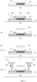
FIG. 2 is a schematic diagram of sequentially forming an aluminum layer and an anti-oxidation layer having a preset pattern on the base substrate based on the method shown inFIG. 1 ; -
FIG. 3 is a schematic diagram of forming a thin-film transistor on the aluminum layer and the anti-oxidation layer shown inFIG. 2 based on the method shown inFIG. 1 ; and -
FIG. 4 is a schematic diagram of a cross-sectional structure of a display panel according to an embodiment of the present invention. - The following will combine the figures in the embodiment of the present invention to describe each exemplary embodiment provided by the present invention clearly and completely. In the absence of conflict, embodiments and features of embodiments can be combined with each other.
- With reference to
FIG. 1 , which is a manufacturing method for a thin-film transistor according to an embodiment of the present invention. The manufacturing method for a thin-film transistor includes following steps S11∼S17. - S11: sequentially forming an aluminum layer and an anti-oxidation layer having a preset pattern on the base substrate. Wherein, on the base substrate, a first region, a second region and a third region are provided, and arranged adjacently along a direction in parallel with the base substrate. The aluminum layer is formed at the first region, the second region and the third region. The anti-oxidation layer is formed at the second region.
- An embodiment of the present invention can form the aluminum layer and the anti-oxidation layer having a preset pattern on the base substrate by adopting a method combining exposing and etching. With reference to
FIG. 2 , specifically:
Firstly, sequentially forming analuminum layer 21 and ananti-oxidation layer 22 covering thebase substrate 20 on thebase substrate 20. Thebase substrate 20 includes but not limited to a transparent substrate such as a glass substrate, a plastic substrate, or a flexible substrate. The present embodiment can adopt a PVD (Physical Vapor Deposition) method to sequentially form an entire surface of thealuminum layer 21, and an entire surface of ananti-oxidation layer 22, and theanti-oxidation layer 22 can be a Mo (molybdenum) layer. - Then, forming a
photoresist layer 23 having an entire surface of an even thickness on theanti-oxidation layer 22. - Then, adopting a half-tone mask to expose the
photoresist layer 23. The photoresist which is fully exposed can be removed by a developer. The photoresist which is not exposed is not removed by the developer. The photoresist which is half exposed can be partially removed such that thephotoresist layer 23 after being exposed is only reserved in thefirst region 201, thesecond region 202 and thethird region 203 as shown inFIG. 2 . Besides, a thickness of thephotoresist layer 23 after being exposed at thesecond region 202 is greater than a thickness of thephotoresist layer 23 after being exposed at thefirst region 201, and is also greater than a thickness of thephotoresist layer 23 after being exposed at thethird region 203. The thickness of thephotoresist layer 23 after being exposed at thefirst region 201 and thesecond region 202 can be the same. - Then, performing a first etching process in order to remove the
aluminum layer 21 and theanti-oxidation layer 22 not covered by thephotoresist layer 23. The first etching process can adopt a wet etching, that is, through a corrosion solution to submerge thephotoresist layer 23. Thealuminum layer 21 and theanti-oxidation layer 22 not covered by thephotoresist layer 23 will generate a chemical reaction with the corrosion solution so as to be dissolved in the corrosion solution. Thealuminum layer 21 and theanti-oxidation layer 22 covered by thephotoresist layer 23 will not generate a chemical reaction with the corrosion solution because of a barrier function of thephotoresist layer 23 so as to be reserved. - Furthermore, ashing the
photoresist layer 23 in order to remove thephotoresist layer 23 located at thefirst region 201 and thethird region 203. Comparing with thephotoresist layer 23 after being exposed, the thickness of thephotoresist layer 23 at the second region after ashing become smaller, but can be reserved. - Performing a second etching process in order to remove the
anti-oxidation layer 22 located at thefirst region 201 and thethird region 203. The second etching process can adopt a dry etching. For example, adopting bombarding theanti-oxidation layer 22 at thefirst region 201 and thethird region 203 using a plasma gas in order to remove theanti-oxidation layer 22 at the two regions. Then, stop etching. After the second etching process, thealuminum layer 21 at thefirst region 201 and thethird region 203 are unchanged. - Finally, removing the
photoresist layer 23 located at thesecond region 202. At this point, thealuminum layer 21 and theanti-oxidation layer 22 having a preset pattern are obtained. That is, along a direction in parallel with thebase substrate 20, thealuminum layer 21 is formed at thefirst region 201, thesecond region 202 and thethird region 203. An orthographic projection of theanti-oxidation layer 22 on thebase substrate 20 is overlapped with thesecond region 202. - Of course, after forming an entire surface of the
aluminum layer 21 and an entire surface of theanti-oxidation layer 22, another embodiment of the present invention can only form aphotoresist layer 23 at theanti-oxidation layer 22 located at thesecond region 202. That is, an orthographic projection of thephotoresist layer 23 on thebase substrate 20 is overlapped with thesecond region 202. Then, performing a dry etching to theanti-oxidation layer 22 not covered by thephotoresist layer 23 in order to remove theanti-oxidation layer 22 not covered by thephotoresist layer 23. Finally, removing thephotoresist layer 23 in order to obtain thealuminum layer 21 and theanti-oxidation layer 22 having a preset pattern. - Or, in another embodiment of the present invention, it can also adopt a PVD method to directly form the
aluminum layer 21 and theanti-oxidation layer 22 having a preset pattern on thebase substrate 20. - S12: forming an amorphous oxide semiconductor layer covering the aluminum layer on the anti-oxidation layer.
- With reference to
FIG. 2 andFIG. 3 , the present embodiment can adopt a PVD method to form an entire surface of an amorphousoxide semiconductor layer 24 covering on thebase substrate 20. The material of the amorphousoxide semiconductor layer 24 includes but not limited to IGZO. Then, the present embodiment can only reserve the amorphousoxide semiconductor layer 24 located at thefirst region 201, thesecond region 202 and thethird region 203 through photoresist coating, exposing and etching. - S13: performing an annealing treatment to the amorphous oxide semiconductor layer such that in the annealing treatment, the aluminum layer at the first region and the third region generates an oxidation reaction in order to form Al2O3. Besides, the amorphous oxide semiconductor layer at the first region and the third region generates a crystallization reaction in order to form a source contact region and a drain contact region, and form a channel region at the second region shielded by the anti-oxidation layer.
- In the annealing process, the
aluminum layer 21 combines with oxygen ions in the amorphousoxide semiconductor layer 24 to form an Al2O3 layer. When the amorphousoxide semiconductor layer 24 loses the oxygen ions, oxygen defects are increased such that at doped region of two terminals of the amorphous oxide semiconductor layer 24 (that is, a portion of the amorphousoxide semiconductor layer 24 located at thefirst region 201 and the third region 203), a dopedsemiconductor layer 25 is formed such as N+IGZO layer. The crystal direction is from thefirst region 201 and thethird region 203 toward thesecond region 202. The directional crystallization can ensure the crystallization efficiency and crystallization uniformity in order to reduce the affection of the grain boundaries to the electron mobility and leakage current in order to guarantee the electrical characteristics of thesemiconductor layer 25. - After the annealing treatment, two terminals of the amorphous
oxide semiconductor layer 24 respectively forms a source contact region and a drain contact region, and a middle portion of the amorphousoxide semiconductor layer 24 shielded by the anti-oxidation layer 22 (that is a portion located in the second region 202) forms a channel region. Besides, after the crystallization is finished, doped ions in the channel region is less and the electron mobility is lower in order to reduce the leakage current of the TFT. The doped ions in the source contact region and the drain contact region is more, the electron mobility is higher so as to decrease a contact impedance of the source electrode and the drain electrode of TFT formed subsequently. - Thus, the present embodiment can obtain a
semiconductor layer 25 having a good electrical property through the annealing treatment. Besides, because the process of the annealing treatment is simple, the present embodiment can simplify the manufacturing process, which is beneficial to the production efficiency and decrease the production cost. - Wherein, the
anti-oxidation layer 22 is used for insulating the amorphousoxide semiconductor layer 24 and thealuminum layer 21, preventing the oxygen ions of the amorphousoxide semiconductor layer 24 at thesecond region 202 from combining with thealuminum layer 21 so as to form the Al2O3 layer. Accordingly, theanti-oxidation layer 22 of the present embodiment requires adopting a material not easily to be oxidized such as molybdenum or titanium. - S14: forming a gate insulation layer on the amorphous oxide semiconductor layer after being performed with the annealing treatment.
- The present embodiment can adopt a CVD (Chemical Vapor Deposition) method to form the gate insulation layer (GI) 26 on the
semiconductor layer 25. Thegate insulation layer 26 is an entire surface structure covering thebase substrate 20. Wherein, the material of thegate insulation layer 26 can be silicon oxide (SiOx). Of course, thegate insulation layer 26 can also include a silicone compound layer and silicon nitride compound layer sequentially formed on thesemiconductor layer 25 such as silicon dioxide (Si02) and silicon nitride (Si3N4) in order to further increase the wear resistance ability and the insulation ability of thegate insulation layer 26. - S15: forming a gate electrode pattern on the gate insulation layer, the gate electrode pattern is located between the source contact region and the drain contact region, and located correspondingly above the channel region.
- The present embodiment can adopt patterning processes such as photoresist coating, exposing, developing and etching to form the
gate electrode pattern 271 having a preset pattern. Because thegate electrode pattern 271 is located above thesemiconductor layer 25, the TFT of the present embedment can be regarded as a top gate design. Therefore, in the exposing process, the present embodiment can adopt a photolithography process illuminated at a back surface in order to form thegate electrode pattern 271 on thegate insulation layer 26. The photolithography process utilizes the aluminum layer after being performed with an annealing treatment (that is, thealuminum layer 21 at the second region 202) as a light-shielding layer, and illuminating at a side of the light-shielding layer back to theanti-oxidation layer 22 so as to omit a mask using as a light-shielding layer in the conventional art in order to further simplify the manufacturing process. - S16: forming an interlayer dielectric layer on the gate electrode pattern.
- The present embodiment can adopt a CVD method to form an
interlayer dielectric layer 28 on thegate electrode pattern 271. The interlayer dielectric layer (IDL, as known as a dielectric layer) 28 is an entire surface structure covering on thegate insulation layer 26. - S17: forming a source electrode pattern and a drain electrode pattern on the interlayer dielectric layer, the source electrode pattern is connected with the source contact region and the drain electrode pattern is connected with the drain contact region.
- With reference to
FIG. 3 , the present embodiment can form contact holes 291, 292 through photoresist coating, exposing, developing and etching. The contact holes 291, 292 both passes through thegate insulation layer 26 and theinterlayer dielectric layer 28, and exposes upper surfaces of the source contact region and drain contact region of thesemiconductor layer 25. Then, the present embodiment can adopt a PVD method and a patterning process to form thesource electrode pattern 272 and thedrain electrode pattern 273 on theinterlayer dielectric layer 28, thesource electrode pattern 272 is connected with the source contact region of thesemiconductor layer 25 through thecontact hole 291, and thedrain electrode pattern 273 is connected with the drain contact region of thesemiconductor layer 25 through thecontact hole 292. - Through the above method, the thin-film transistor required by the present invention can be obtained.
- The present invention also provides a display panel. As shown in
FIG. 4 , the liquidcrystal display panel 40 can include afirst substrate 41 and asecond substrate 42. The above thin-film transistor can be form on thefirst substrate 41 or thesecond substrate 42. Therefore, thedisplay panel 40 also has the above beneficial effect. Wherein, thedisplay panel 40 can be a liquid crystal display panel, or an AMOLED (Active-matrix organic light emitting diode). - The above embodiments of the present invention are not used to limit the claims of this invention. Any use of the content in the specification or in the drawings of the present invention which produces equivalent structures or equivalent processes, or directly or indirectly used in other related technical fields is still covered by the claims in the present invention.
Claims (16)
- A manufacturing method for a thin-film transistor, comprising:sequentially forming an aluminum layer and an anti-oxidation layer having a preset pattern on a base substrate, wherein the base substrate is provided with a first region, a second region and a third region arranged adjacently along a direction in parallel with the base substrate, the aluminum layer is formed in the first region, the second region and the third region, and the anti-oxidation layer is formed in the second region;forming an amorphous oxide semiconductor layer covering the aluminum layer on the anti-oxidation layer;performing an annealing treatment to the amorphous oxide semiconductor layer such that in the annealing treatment, the aluminum layer at the first region and the third region generates an oxidation reaction in order to form Al2O3; the amorphous oxide semiconductor layer at the first region and the third region generates a crystallization reaction in order to form a source contact region and a drain contact region, and form a channel region at the second region shielded by the anti-oxidation layer;forming a gate insulation layer on the amorphous oxide semiconductor layer after being performed with the annealing treatment;forming a gate electrode pattern on the gate insulation layer, the gate electrode pattern is located between the source contact region and the drain contact region, and located correspondingly above the channel region;forming an interlayer dielectric layer on the gate electrode pattern; andforming a source electrode pattern and a drain electrode pattern on the interlayer dielectric layer, the source electrode pattern is connected with the source contact region and the drain electrode pattern is connected with the drain contact region.
- The manufacturing method according to claim 1, wherein, the step of sequentially forming an aluminum layer and an anti-oxidation layer having a preset pattern on a base substrate comprises:sequentially forming an aluminum layer and an anti-oxidation layer covering the base substrate on the base substrate;forming a photoresist layer on the anti-oxidation layer;adopting a half-tone mask to expose the photoresist layer such that the photoresist layer after being exposed is formed at the first region, the second region and the third region; a thickness of the photoresist layer at the second region is greater than a thickness of the photoresist layer at anyone of the first region and the third region;performing a first etching process in order to remove the aluminum layer and the anti-oxidation layer not covered by the photoresist layer after being exposed;ashing the photoresist layer after being exposed in order to remove the photoresist layer located at the first region and the third region, and reserved the photoresist layer at the second region;performing a second etching process in order to remove the anti-oxidation layer located at the first region and the third region, and not being shielded by the photoresist layer at the second region; andremoving the photoresist layer located at the second region.
- The manufacturing method according to claim 2, wherein, the first etching process adopts a wet etching, and the second etching process adopts a dry etching.
- The manufacturing method according to claim 1, wherein, the step of sequentially forming an aluminum layer and an anti-oxidation layer having a preset pattern on a base substrate comprises:sequentially forming an aluminum layer and an anti-oxidation layer covering the base substrate on the base substrate;forming a photoresist layer on the anti-oxidation layer, and an orthographic projection of the photoresist layer on the base substrate is overlapped with the second region; andperforming an etching process to the anti-oxidation layer not covered by the photoresist layer in order to remove the anti-oxidation layer not covered by the photoresist layer.
- The manufacturing method according to claim 4, wherein, adopting a dry etching to etch the anti-oxidation layer not covered by the photoresist layer.
- The manufacturing method according to claim 1, wherein, the anti-oxidation layer includes a molybdenum layer.
- The manufacturing method according to claim 1, wherein, adopting a photolithography process illuminated at a back surface in order to form the gate electrode pattern on the gate insulation layer, and the photolithography process utilizes the aluminum layer at the second region as a light-shielding layer, and illuminating at a side of the light-shielding layer back to the anti-oxidation layer.
- The manufacturing method according to claim 1, wherein, the step of forming a source electrode pattern and a drain electrode pattern on the interlayer dielectric layer comprise:forming two contact holes that both passes through the gate insulation layer and the interlayer dielectric layer, and the two contact holes respectively expose the source contact region and the drain contact region; andforming a source electrode pattern and a drain electrode pattern on the interlayer dielectric layer, and the source electrode pattern and the drain electrode pattern are respectively formed in the two contact holes.
- A thin-film transistor, comprising:a Al2O3 layer and an aluminum layer having a preset pattern on a base substrate, wherein the base substrate is provided with a first region, a second region and a third region arranged adjacently along a direction in parallel with the base substrate, the Al2O3 layer is formed in the first region and the third region, and the aluminum layer is formed in the second region;an anti-oxidation layer located on the aluminum layer, and an orthographic projection of the anti-oxidation layer on the base substrate is overlapped with the second region;a semiconductor layer located on the anti-oxidation layer and including a source contact region, a drain contact region and a channel region, an orthographic projection of the source contact region on the base substrate is overlapped with the first region, an orthographic projection of the drain contact region on the base substrate is overlapped with the third region, and an orthographic projection of the channel region on the base substrate is overlapped with the second region;a gate insulation layer located on the semiconductor layer;a gate electrode pattern located on the gate insulation layer, and the gate electrode pattern is located between the source contact region and the drain contact region, and located correspondingly above the channel region;an interlayer dielectric layer located on the gate electrode pattern; anda source electrode pattern and a drain electrode pattern on the interlayer dielectric layer, wherein the source electrode pattern is connected with the source contact region and the drain electrode pattern is connected with the drain contact region.
- The thin-film transistor according to claim 9, wherein, the anti-oxidation layer includes a molybdenum layer.
- The thin-film transistor according to claim 9, wherein, the gate insulation layer includes a silicone compound layer and silicon nitride compound layer sequentially formed on the semiconductor layer.
- The thin-film transistor according to claim 9, wherein, the thin-film transistor further includes two contact holes that both passes through the gate insulation layer and the interlayer dielectric layer, and the two contact holes respectively expose the source contact region and the drain contact region, the source electrode pattern and the drain electrode pattern are respectively formed in the two contact holes.
- A display panel having a thin-film transistor, and the thin-film transistor comprises:a Al2O3 layer and an aluminum layer having a preset pattern on a base substrate, wherein the base substrate is provided with a first region, a second region and a third region arranged adjacently along a direction in parallel with the base substrate, the Al2O3 layer is formed in the first region and the third region, and the aluminum layer is formed in the second region;an anti-oxidation layer located on the aluminum layer, and an orthographic projection of the anti-oxidation layer on the base substrate is overlapped with the second region;a semiconductor layer located on the anti-oxidation layer and including a source contact region, a drain contact region and a channel region, an orthographic projection of the source contact region on the base substrate is overlapped with the first region, an orthographic projection of the drain contact region on the base substrate is overlapped with the third region, and an orthographic projection of the channel region on the base substrate is overlapped with the second region;a gate insulation layer located on the semiconductor layer;a gate electrode pattern located on the gate insulation layer, and the gate electrode pattern is located between the source contact region and the drain contact region, and located correspondingly above the channel region;an interlayer dielectric layer located on the gate electrode pattern; anda source electrode pattern and a drain electrode pattern on the interlayer dielectric layer, wherein the source electrode pattern is connected with the source contact region and the drain electrode pattern is connected with the drain contact region.
- The display panel according to claim 13, wherein, the anti-oxidation layer includes a molybdenum layer.
- The display panel according to claim 13, wherein, the gate insulation layer includes a silicone compound layer and silicon nitride compound layer sequentially formed on the semiconductor layer.
- The display panel according to claim 13, wherein, the thin-film transistor further includes two contact holes that both passes through the gate insulation layer and the interlayer dielectric layer, and the two contact holes respectively expose the source contact region and the drain contact region, the source electrode pattern and the drain electrode pattern are respectively formed in the two contact holes.
Applications Claiming Priority (2)
| Application Number | Priority Date | Filing Date | Title |
|---|---|---|---|
| CN201710156787.4A CN106952827A (en) | 2017-03-16 | 2017-03-16 | Thin film transistor (TFT) and its manufacture method, display panel |
| PCT/CN2017/079907 WO2018166018A1 (en) | 2017-03-16 | 2017-04-10 | Thin-film transistor and method for manufacturing same, and display panel |
Publications (2)
| Publication Number | Publication Date |
|---|---|
| EP3598479A1 true EP3598479A1 (en) | 2020-01-22 |
| EP3598479A4 EP3598479A4 (en) | 2020-11-25 |
Family
ID=59472672
Family Applications (1)
| Application Number | Title | Priority Date | Filing Date |
|---|---|---|---|
| EP17900358.7A Withdrawn EP3598479A4 (en) | 2017-03-16 | 2017-04-10 | THIN-FILM TRANSISTOR AND METHOD OF MANUFACTURING THEREOF AND DISPLAY BOARD |
Country Status (6)
| Country | Link |
|---|---|
| US (1) | US10205028B2 (en) |
| EP (1) | EP3598479A4 (en) |
| JP (1) | JP6829775B2 (en) |
| KR (1) | KR102205307B1 (en) |
| CN (1) | CN106952827A (en) |
| WO (1) | WO2018166018A1 (en) |
Families Citing this family (1)
| Publication number | Priority date | Publication date | Assignee | Title |
|---|---|---|---|---|
| CN108054192B (en) | 2018-01-19 | 2019-12-24 | 武汉华星光电半导体显示技术有限公司 | Flexible AMOLED substrate and manufacturing method thereof |
Family Cites Families (19)
| Publication number | Priority date | Publication date | Assignee | Title |
|---|---|---|---|---|
| JP3067949B2 (en) * | 1994-06-15 | 2000-07-24 | シャープ株式会社 | Electronic device and liquid crystal display device |
| KR101496148B1 (en) * | 2008-05-15 | 2015-02-27 | 삼성전자주식회사 | Semiconductor device and manufacturing method thereof |
| KR101476817B1 (en) * | 2009-07-03 | 2014-12-26 | 가부시키가이샤 한도오따이 에네루기 켄큐쇼 | Display device including transistor and manufacturing method thereof |
| JP5584103B2 (en) * | 2009-12-04 | 2014-09-03 | 株式会社半導体エネルギー研究所 | Semiconductor device |
| JP5708910B2 (en) * | 2010-03-30 | 2015-04-30 | ソニー株式会社 | THIN FILM TRANSISTOR, MANUFACTURING METHOD THEREOF, AND DISPLAY DEVICE |
| KR20110125105A (en) * | 2010-05-12 | 2011-11-18 | 엘지디스플레이 주식회사 | Oxide thin film transistor and its manufacturing method |
| US9209314B2 (en) * | 2010-06-16 | 2015-12-08 | Semiconductor Energy Laboratory Co., Ltd. | Field effect transistor |
| JP2012015436A (en) * | 2010-07-05 | 2012-01-19 | Sony Corp | Thin film transistor and display device |
| JP5917035B2 (en) * | 2010-07-26 | 2016-05-11 | 株式会社半導体エネルギー研究所 | Semiconductor device |
| KR102072244B1 (en) * | 2011-11-30 | 2020-01-31 | 가부시키가이샤 한도오따이 에네루기 켄큐쇼 | Semiconductor device and method for manufacturing the same |
| US9653614B2 (en) * | 2012-01-23 | 2017-05-16 | Semiconductor Energy Laboratory Co., Ltd. | Semiconductor device and method for manufacturing the same |
| CN103219391B (en) | 2013-04-07 | 2016-03-02 | 京东方科技集团股份有限公司 | A kind of thin-film transistor and preparation method thereof, array base palte and display unit |
| CN103715094B (en) * | 2013-12-27 | 2017-02-01 | 京东方科技集团股份有限公司 | Thin film thyristor and manufacturing method thereof, array substrate and manufacturing method thereof and display device |
| KR102188690B1 (en) * | 2014-01-20 | 2020-12-09 | 삼성디스플레이 주식회사 | Thin film transistor, method of manufacturing the thin film transistor and flat panel display device havint the thin film transistor |
| CN103972110B (en) * | 2014-04-22 | 2016-02-24 | 京东方科技集团股份有限公司 | Thin-film transistor and preparation method thereof, array base palte, display unit |
| TWI555150B (en) | 2014-05-27 | 2016-10-21 | 財團法人工業技術研究院 | Electronic components and their methods |
| CN106206743B (en) * | 2015-05-04 | 2020-04-28 | 清华大学 | Thin film transistor, preparation method thereof, thin film transistor panel and display device |
| JPWO2016181256A1 (en) * | 2015-05-12 | 2018-03-08 | 株式会社半導体エネルギー研究所 | Semiconductor devices, electronic components and electronic equipment |
| CN105938800A (en) * | 2016-07-01 | 2016-09-14 | 深圳市华星光电技术有限公司 | Thin film transistor manufacture method and array substrate manufacture method |
-
2017
- 2017-03-16 CN CN201710156787.4A patent/CN106952827A/en active Pending
- 2017-04-10 WO PCT/CN2017/079907 patent/WO2018166018A1/en not_active Ceased
- 2017-04-10 JP JP2019549372A patent/JP6829775B2/en active Active
- 2017-04-10 KR KR1020197030018A patent/KR102205307B1/en active Active
- 2017-04-10 EP EP17900358.7A patent/EP3598479A4/en not_active Withdrawn
- 2017-04-10 US US15/533,013 patent/US10205028B2/en active Active
Also Published As
| Publication number | Publication date |
|---|---|
| KR102205307B1 (en) | 2021-01-21 |
| EP3598479A4 (en) | 2020-11-25 |
| KR20190124788A (en) | 2019-11-05 |
| JP6829775B2 (en) | 2021-02-10 |
| US10205028B2 (en) | 2019-02-12 |
| WO2018166018A1 (en) | 2018-09-20 |
| CN106952827A (en) | 2017-07-14 |
| JP2020512689A (en) | 2020-04-23 |
| US20180269331A1 (en) | 2018-09-20 |
Similar Documents
| Publication | Publication Date | Title |
|---|---|---|
| CN109300917B (en) | Array substrate, preparation method thereof and display panel | |
| CN107017287B (en) | Thin film transistor, display device, and method for manufacturing thin film transistor | |
| US8759832B2 (en) | Semiconductor device and electroluminescent device and method of making the same | |
| US9437627B2 (en) | Thin film transistor and manufacturing method thereof | |
| US10707236B2 (en) | Array substrate, manufacturing method therefor and display device | |
| US9859391B2 (en) | Thin film transistor, display device, and method for manufacturing thin film transistor | |
| US10290663B2 (en) | Manufacturing method of thin film transistor and manufacturing method of array substrate | |
| US9704998B2 (en) | Thin film transistor and method of manufacturing the same, display substrate, and display apparatus | |
| WO2014166176A1 (en) | Thin-film transistor and manufacturing method thereof, array base plate and display apparatus | |
| US10249654B1 (en) | Manufacturing method of top-gate TFT and top-gate TFT | |
| CN107195583B (en) | A kind of OLED display panel and preparation method thereof | |
| CN108550625B (en) | Thin film transistor and method of making the same | |
| WO2017070868A1 (en) | Manufacturing method for n-type tft | |
| US11139357B2 (en) | Organic light-emitting diode display substrate, manufacturing method thereof, and display device | |
| CN110993610A (en) | Array substrate, preparation method thereof and display panel | |
| CN110098201A (en) | Transistor device and its manufacturing method, display base plate, display device | |
| KR102148957B1 (en) | Display substrate and method of manufacturing a display substrate | |
| CN109166802A (en) | LTPS array substrate and its manufacturing method, display panel | |
| US20190051713A1 (en) | Manufacturing method of tft substrate, tft substrate, and oled display panel | |
| US10916641B2 (en) | Thin film transistor, method of manufacturing thin film transistor, and manufacturing system | |
| CN104681626A (en) | Oxide thin film transistor as well as manufacture and array substrate thereof | |
| US10205028B2 (en) | Thin-film transistor, manufacturing method for the same, display panel | |
| WO2016201610A1 (en) | Metal oxide thin-film transistor and preparation method therefor, and display panel and display device | |
| EP3657547A1 (en) | Fabrication method for top-gate thin film transistor | |
| US12507478B2 (en) | Array substrate, method for fabricating same, and display panel |
Legal Events
| Date | Code | Title | Description |
|---|---|---|---|
| STAA | Information on the status of an ep patent application or granted ep patent |
Free format text: STATUS: THE INTERNATIONAL PUBLICATION HAS BEEN MADE |
|
| PUAI | Public reference made under article 153(3) epc to a published international application that has entered the european phase |
Free format text: ORIGINAL CODE: 0009012 |
|
| STAA | Information on the status of an ep patent application or granted ep patent |
Free format text: STATUS: REQUEST FOR EXAMINATION WAS MADE |
|
| 17P | Request for examination filed |
Effective date: 20191014 |
|
| AK | Designated contracting states |
Kind code of ref document: A1 Designated state(s): AL AT BE BG CH CY CZ DE DK EE ES FI FR GB GR HR HU IE IS IT LI LT LU LV MC MK MT NL NO PL PT RO RS SE SI SK SM TR |
|
| AX | Request for extension of the european patent |
Extension state: BA ME |
|
| DAV | Request for validation of the european patent (deleted) | ||
| DAX | Request for extension of the european patent (deleted) | ||
| A4 | Supplementary search report drawn up and despatched |
Effective date: 20201023 |
|
| RIC1 | Information provided on ipc code assigned before grant |
Ipc: H01L 29/786 20060101ALI20201019BHEP Ipc: H01L 29/08 20060101ALI20201019BHEP Ipc: H01L 21/34 20060101AFI20201019BHEP |
|
| STAA | Information on the status of an ep patent application or granted ep patent |
Free format text: STATUS: THE APPLICATION IS DEEMED TO BE WITHDRAWN |
|
| 18D | Application deemed to be withdrawn |
Effective date: 20210521 |