EP3598427A1 - Pixel driving circuit and oled display device - Google Patents
Pixel driving circuit and oled display device Download PDFInfo
- Publication number
- EP3598427A1 EP3598427A1 EP17900438.7A EP17900438A EP3598427A1 EP 3598427 A1 EP3598427 A1 EP 3598427A1 EP 17900438 A EP17900438 A EP 17900438A EP 3598427 A1 EP3598427 A1 EP 3598427A1
- Authority
- EP
- European Patent Office
- Prior art keywords
- tft
- signal
- electrically connected
- data signal
- voltage level
- Prior art date
- Legal status (The legal status is an assumption and is not a legal conclusion. Google has not performed a legal analysis and makes no representation as to the accuracy of the status listed.)
- Withdrawn
Links
Images



Classifications
-
- H—ELECTRICITY
- H10—SEMICONDUCTOR DEVICES; ELECTRIC SOLID-STATE DEVICES NOT OTHERWISE PROVIDED FOR
- H10D—INORGANIC ELECTRIC SEMICONDUCTOR DEVICES
- H10D86/00—Integrated devices formed in or on insulating or conducting substrates, e.g. formed in silicon-on-insulator [SOI] substrates or on stainless steel or glass substrates
- H10D86/40—Integrated devices formed in or on insulating or conducting substrates, e.g. formed in silicon-on-insulator [SOI] substrates or on stainless steel or glass substrates characterised by multiple TFTs
-
- G—PHYSICS
- G09—EDUCATION; CRYPTOGRAPHY; DISPLAY; ADVERTISING; SEALS
- G09G—ARRANGEMENTS OR CIRCUITS FOR CONTROL OF INDICATING DEVICES USING STATIC MEANS TO PRESENT VARIABLE INFORMATION
- G09G3/00—Control arrangements or circuits, of interest only in connection with visual indicators other than cathode-ray tubes
- G09G3/20—Control arrangements or circuits, of interest only in connection with visual indicators other than cathode-ray tubes for presentation of an assembly of a number of characters, e.g. a page, by composing the assembly by combination of individual elements arranged in a matrix no fixed position being assigned to or needed to be assigned to the individual characters or partial characters
- G09G3/22—Control arrangements or circuits, of interest only in connection with visual indicators other than cathode-ray tubes for presentation of an assembly of a number of characters, e.g. a page, by composing the assembly by combination of individual elements arranged in a matrix no fixed position being assigned to or needed to be assigned to the individual characters or partial characters using controlled light sources
- G09G3/30—Control arrangements or circuits, of interest only in connection with visual indicators other than cathode-ray tubes for presentation of an assembly of a number of characters, e.g. a page, by composing the assembly by combination of individual elements arranged in a matrix no fixed position being assigned to or needed to be assigned to the individual characters or partial characters using controlled light sources using electroluminescent panels
- G09G3/32—Control arrangements or circuits, of interest only in connection with visual indicators other than cathode-ray tubes for presentation of an assembly of a number of characters, e.g. a page, by composing the assembly by combination of individual elements arranged in a matrix no fixed position being assigned to or needed to be assigned to the individual characters or partial characters using controlled light sources using electroluminescent panels semiconductive, e.g. using light-emitting diodes [LED]
- G09G3/3208—Control arrangements or circuits, of interest only in connection with visual indicators other than cathode-ray tubes for presentation of an assembly of a number of characters, e.g. a page, by composing the assembly by combination of individual elements arranged in a matrix no fixed position being assigned to or needed to be assigned to the individual characters or partial characters using controlled light sources using electroluminescent panels semiconductive, e.g. using light-emitting diodes [LED] organic, e.g. using organic light-emitting diodes [OLED]
- G09G3/3266—Details of drivers for scan electrodes
-
- G—PHYSICS
- G09—EDUCATION; CRYPTOGRAPHY; DISPLAY; ADVERTISING; SEALS
- G09G—ARRANGEMENTS OR CIRCUITS FOR CONTROL OF INDICATING DEVICES USING STATIC MEANS TO PRESENT VARIABLE INFORMATION
- G09G3/00—Control arrangements or circuits, of interest only in connection with visual indicators other than cathode-ray tubes
- G09G3/20—Control arrangements or circuits, of interest only in connection with visual indicators other than cathode-ray tubes for presentation of an assembly of a number of characters, e.g. a page, by composing the assembly by combination of individual elements arranged in a matrix no fixed position being assigned to or needed to be assigned to the individual characters or partial characters
- G09G3/22—Control arrangements or circuits, of interest only in connection with visual indicators other than cathode-ray tubes for presentation of an assembly of a number of characters, e.g. a page, by composing the assembly by combination of individual elements arranged in a matrix no fixed position being assigned to or needed to be assigned to the individual characters or partial characters using controlled light sources
- G09G3/30—Control arrangements or circuits, of interest only in connection with visual indicators other than cathode-ray tubes for presentation of an assembly of a number of characters, e.g. a page, by composing the assembly by combination of individual elements arranged in a matrix no fixed position being assigned to or needed to be assigned to the individual characters or partial characters using controlled light sources using electroluminescent panels
- G09G3/32—Control arrangements or circuits, of interest only in connection with visual indicators other than cathode-ray tubes for presentation of an assembly of a number of characters, e.g. a page, by composing the assembly by combination of individual elements arranged in a matrix no fixed position being assigned to or needed to be assigned to the individual characters or partial characters using controlled light sources using electroluminescent panels semiconductive, e.g. using light-emitting diodes [LED]
- G09G3/3208—Control arrangements or circuits, of interest only in connection with visual indicators other than cathode-ray tubes for presentation of an assembly of a number of characters, e.g. a page, by composing the assembly by combination of individual elements arranged in a matrix no fixed position being assigned to or needed to be assigned to the individual characters or partial characters using controlled light sources using electroluminescent panels semiconductive, e.g. using light-emitting diodes [LED] organic, e.g. using organic light-emitting diodes [OLED]
- G09G3/3225—Control arrangements or circuits, of interest only in connection with visual indicators other than cathode-ray tubes for presentation of an assembly of a number of characters, e.g. a page, by composing the assembly by combination of individual elements arranged in a matrix no fixed position being assigned to or needed to be assigned to the individual characters or partial characters using controlled light sources using electroluminescent panels semiconductive, e.g. using light-emitting diodes [LED] organic, e.g. using organic light-emitting diodes [OLED] using an active matrix
- G09G3/3233—Control arrangements or circuits, of interest only in connection with visual indicators other than cathode-ray tubes for presentation of an assembly of a number of characters, e.g. a page, by composing the assembly by combination of individual elements arranged in a matrix no fixed position being assigned to or needed to be assigned to the individual characters or partial characters using controlled light sources using electroluminescent panels semiconductive, e.g. using light-emitting diodes [LED] organic, e.g. using organic light-emitting diodes [OLED] using an active matrix with pixel circuitry controlling the current through the light-emitting element
- G09G3/3241—Control arrangements or circuits, of interest only in connection with visual indicators other than cathode-ray tubes for presentation of an assembly of a number of characters, e.g. a page, by composing the assembly by combination of individual elements arranged in a matrix no fixed position being assigned to or needed to be assigned to the individual characters or partial characters using controlled light sources using electroluminescent panels semiconductive, e.g. using light-emitting diodes [LED] organic, e.g. using organic light-emitting diodes [OLED] using an active matrix with pixel circuitry controlling the current through the light-emitting element the current through the light-emitting element being set using a data current provided by the data driver, e.g. by using a two-transistor current mirror
-
- G—PHYSICS
- G09—EDUCATION; CRYPTOGRAPHY; DISPLAY; ADVERTISING; SEALS
- G09G—ARRANGEMENTS OR CIRCUITS FOR CONTROL OF INDICATING DEVICES USING STATIC MEANS TO PRESENT VARIABLE INFORMATION
- G09G3/00—Control arrangements or circuits, of interest only in connection with visual indicators other than cathode-ray tubes
- G09G3/20—Control arrangements or circuits, of interest only in connection with visual indicators other than cathode-ray tubes for presentation of an assembly of a number of characters, e.g. a page, by composing the assembly by combination of individual elements arranged in a matrix no fixed position being assigned to or needed to be assigned to the individual characters or partial characters
- G09G3/22—Control arrangements or circuits, of interest only in connection with visual indicators other than cathode-ray tubes for presentation of an assembly of a number of characters, e.g. a page, by composing the assembly by combination of individual elements arranged in a matrix no fixed position being assigned to or needed to be assigned to the individual characters or partial characters using controlled light sources
- G09G3/30—Control arrangements or circuits, of interest only in connection with visual indicators other than cathode-ray tubes for presentation of an assembly of a number of characters, e.g. a page, by composing the assembly by combination of individual elements arranged in a matrix no fixed position being assigned to or needed to be assigned to the individual characters or partial characters using controlled light sources using electroluminescent panels
- G09G3/32—Control arrangements or circuits, of interest only in connection with visual indicators other than cathode-ray tubes for presentation of an assembly of a number of characters, e.g. a page, by composing the assembly by combination of individual elements arranged in a matrix no fixed position being assigned to or needed to be assigned to the individual characters or partial characters using controlled light sources using electroluminescent panels semiconductive, e.g. using light-emitting diodes [LED]
- G09G3/3208—Control arrangements or circuits, of interest only in connection with visual indicators other than cathode-ray tubes for presentation of an assembly of a number of characters, e.g. a page, by composing the assembly by combination of individual elements arranged in a matrix no fixed position being assigned to or needed to be assigned to the individual characters or partial characters using controlled light sources using electroluminescent panels semiconductive, e.g. using light-emitting diodes [LED] organic, e.g. using organic light-emitting diodes [OLED]
- G09G3/3225—Control arrangements or circuits, of interest only in connection with visual indicators other than cathode-ray tubes for presentation of an assembly of a number of characters, e.g. a page, by composing the assembly by combination of individual elements arranged in a matrix no fixed position being assigned to or needed to be assigned to the individual characters or partial characters using controlled light sources using electroluminescent panels semiconductive, e.g. using light-emitting diodes [LED] organic, e.g. using organic light-emitting diodes [OLED] using an active matrix
-
- G—PHYSICS
- G09—EDUCATION; CRYPTOGRAPHY; DISPLAY; ADVERTISING; SEALS
- G09G—ARRANGEMENTS OR CIRCUITS FOR CONTROL OF INDICATING DEVICES USING STATIC MEANS TO PRESENT VARIABLE INFORMATION
- G09G3/00—Control arrangements or circuits, of interest only in connection with visual indicators other than cathode-ray tubes
- G09G3/20—Control arrangements or circuits, of interest only in connection with visual indicators other than cathode-ray tubes for presentation of an assembly of a number of characters, e.g. a page, by composing the assembly by combination of individual elements arranged in a matrix no fixed position being assigned to or needed to be assigned to the individual characters or partial characters
- G09G3/22—Control arrangements or circuits, of interest only in connection with visual indicators other than cathode-ray tubes for presentation of an assembly of a number of characters, e.g. a page, by composing the assembly by combination of individual elements arranged in a matrix no fixed position being assigned to or needed to be assigned to the individual characters or partial characters using controlled light sources
- G09G3/30—Control arrangements or circuits, of interest only in connection with visual indicators other than cathode-ray tubes for presentation of an assembly of a number of characters, e.g. a page, by composing the assembly by combination of individual elements arranged in a matrix no fixed position being assigned to or needed to be assigned to the individual characters or partial characters using controlled light sources using electroluminescent panels
- G09G3/32—Control arrangements or circuits, of interest only in connection with visual indicators other than cathode-ray tubes for presentation of an assembly of a number of characters, e.g. a page, by composing the assembly by combination of individual elements arranged in a matrix no fixed position being assigned to or needed to be assigned to the individual characters or partial characters using controlled light sources using electroluminescent panels semiconductive, e.g. using light-emitting diodes [LED]
- G09G3/3208—Control arrangements or circuits, of interest only in connection with visual indicators other than cathode-ray tubes for presentation of an assembly of a number of characters, e.g. a page, by composing the assembly by combination of individual elements arranged in a matrix no fixed position being assigned to or needed to be assigned to the individual characters or partial characters using controlled light sources using electroluminescent panels semiconductive, e.g. using light-emitting diodes [LED] organic, e.g. using organic light-emitting diodes [OLED]
- G09G3/3225—Control arrangements or circuits, of interest only in connection with visual indicators other than cathode-ray tubes for presentation of an assembly of a number of characters, e.g. a page, by composing the assembly by combination of individual elements arranged in a matrix no fixed position being assigned to or needed to be assigned to the individual characters or partial characters using controlled light sources using electroluminescent panels semiconductive, e.g. using light-emitting diodes [LED] organic, e.g. using organic light-emitting diodes [OLED] using an active matrix
- G09G3/3233—Control arrangements or circuits, of interest only in connection with visual indicators other than cathode-ray tubes for presentation of an assembly of a number of characters, e.g. a page, by composing the assembly by combination of individual elements arranged in a matrix no fixed position being assigned to or needed to be assigned to the individual characters or partial characters using controlled light sources using electroluminescent panels semiconductive, e.g. using light-emitting diodes [LED] organic, e.g. using organic light-emitting diodes [OLED] using an active matrix with pixel circuitry controlling the current through the light-emitting element
-
- H—ELECTRICITY
- H10—SEMICONDUCTOR DEVICES; ELECTRIC SOLID-STATE DEVICES NOT OTHERWISE PROVIDED FOR
- H10D—INORGANIC ELECTRIC SEMICONDUCTOR DEVICES
- H10D86/00—Integrated devices formed in or on insulating or conducting substrates, e.g. formed in silicon-on-insulator [SOI] substrates or on stainless steel or glass substrates
- H10D86/40—Integrated devices formed in or on insulating or conducting substrates, e.g. formed in silicon-on-insulator [SOI] substrates or on stainless steel or glass substrates characterised by multiple TFTs
- H10D86/60—Integrated devices formed in or on insulating or conducting substrates, e.g. formed in silicon-on-insulator [SOI] substrates or on stainless steel or glass substrates characterised by multiple TFTs wherein the TFTs are in active matrices
-
- G—PHYSICS
- G09—EDUCATION; CRYPTOGRAPHY; DISPLAY; ADVERTISING; SEALS
- G09G—ARRANGEMENTS OR CIRCUITS FOR CONTROL OF INDICATING DEVICES USING STATIC MEANS TO PRESENT VARIABLE INFORMATION
- G09G2300/00—Aspects of the constitution of display devices
- G09G2300/04—Structural and physical details of display devices
- G09G2300/0421—Structural details of the set of electrodes
- G09G2300/043—Compensation electrodes or other additional electrodes in matrix displays related to distortions or compensation signals, e.g. for modifying TFT threshold voltage in column driver
-
- G—PHYSICS
- G09—EDUCATION; CRYPTOGRAPHY; DISPLAY; ADVERTISING; SEALS
- G09G—ARRANGEMENTS OR CIRCUITS FOR CONTROL OF INDICATING DEVICES USING STATIC MEANS TO PRESENT VARIABLE INFORMATION
- G09G2300/00—Aspects of the constitution of display devices
- G09G2300/04—Structural and physical details of display devices
- G09G2300/0439—Pixel structures
-
- G—PHYSICS
- G09—EDUCATION; CRYPTOGRAPHY; DISPLAY; ADVERTISING; SEALS
- G09G—ARRANGEMENTS OR CIRCUITS FOR CONTROL OF INDICATING DEVICES USING STATIC MEANS TO PRESENT VARIABLE INFORMATION
- G09G2300/00—Aspects of the constitution of display devices
- G09G2300/08—Active matrix structure, i.e. with use of active elements, inclusive of non-linear two terminal elements, in the pixels together with light emitting or modulating elements
- G09G2300/0809—Several active elements per pixel in active matrix panels
-
- G—PHYSICS
- G09—EDUCATION; CRYPTOGRAPHY; DISPLAY; ADVERTISING; SEALS
- G09G—ARRANGEMENTS OR CIRCUITS FOR CONTROL OF INDICATING DEVICES USING STATIC MEANS TO PRESENT VARIABLE INFORMATION
- G09G2300/00—Aspects of the constitution of display devices
- G09G2300/08—Active matrix structure, i.e. with use of active elements, inclusive of non-linear two terminal elements, in the pixels together with light emitting or modulating elements
- G09G2300/0809—Several active elements per pixel in active matrix panels
- G09G2300/0819—Several active elements per pixel in active matrix panels used for counteracting undesired variations, e.g. feedback or autozeroing
-
- G—PHYSICS
- G09—EDUCATION; CRYPTOGRAPHY; DISPLAY; ADVERTISING; SEALS
- G09G—ARRANGEMENTS OR CIRCUITS FOR CONTROL OF INDICATING DEVICES USING STATIC MEANS TO PRESENT VARIABLE INFORMATION
- G09G2300/00—Aspects of the constitution of display devices
- G09G2300/08—Active matrix structure, i.e. with use of active elements, inclusive of non-linear two terminal elements, in the pixels together with light emitting or modulating elements
- G09G2300/0809—Several active elements per pixel in active matrix panels
- G09G2300/0842—Several active elements per pixel in active matrix panels forming a memory circuit, e.g. a dynamic memory with one capacitor
-
- G—PHYSICS
- G09—EDUCATION; CRYPTOGRAPHY; DISPLAY; ADVERTISING; SEALS
- G09G—ARRANGEMENTS OR CIRCUITS FOR CONTROL OF INDICATING DEVICES USING STATIC MEANS TO PRESENT VARIABLE INFORMATION
- G09G2300/00—Aspects of the constitution of display devices
- G09G2300/08—Active matrix structure, i.e. with use of active elements, inclusive of non-linear two terminal elements, in the pixels together with light emitting or modulating elements
- G09G2300/0809—Several active elements per pixel in active matrix panels
- G09G2300/0842—Several active elements per pixel in active matrix panels forming a memory circuit, e.g. a dynamic memory with one capacitor
- G09G2300/0861—Several active elements per pixel in active matrix panels forming a memory circuit, e.g. a dynamic memory with one capacitor with additional control of the display period without amending the charge stored in a pixel memory, e.g. by means of additional select electrodes
-
- G—PHYSICS
- G09—EDUCATION; CRYPTOGRAPHY; DISPLAY; ADVERTISING; SEALS
- G09G—ARRANGEMENTS OR CIRCUITS FOR CONTROL OF INDICATING DEVICES USING STATIC MEANS TO PRESENT VARIABLE INFORMATION
- G09G2310/00—Command of the display device
- G09G2310/02—Addressing, scanning or driving the display screen or processing steps related thereto
- G09G2310/0243—Details of the generation of driving signals
- G09G2310/0251—Precharge or discharge of pixel before applying new pixel voltage
-
- G—PHYSICS
- G09—EDUCATION; CRYPTOGRAPHY; DISPLAY; ADVERTISING; SEALS
- G09G—ARRANGEMENTS OR CIRCUITS FOR CONTROL OF INDICATING DEVICES USING STATIC MEANS TO PRESENT VARIABLE INFORMATION
- G09G2310/00—Command of the display device
- G09G2310/02—Addressing, scanning or driving the display screen or processing steps related thereto
- G09G2310/0262—The addressing of the pixel, in a display other than an active matrix LCD, involving the control of two or more scan electrodes or two or more data electrodes, e.g. pixel voltage dependent on signals of two data electrodes
-
- G—PHYSICS
- G09—EDUCATION; CRYPTOGRAPHY; DISPLAY; ADVERTISING; SEALS
- G09G—ARRANGEMENTS OR CIRCUITS FOR CONTROL OF INDICATING DEVICES USING STATIC MEANS TO PRESENT VARIABLE INFORMATION
- G09G2310/00—Command of the display device
- G09G2310/02—Addressing, scanning or driving the display screen or processing steps related thereto
- G09G2310/0264—Details of driving circuits
-
- G—PHYSICS
- G09—EDUCATION; CRYPTOGRAPHY; DISPLAY; ADVERTISING; SEALS
- G09G—ARRANGEMENTS OR CIRCUITS FOR CONTROL OF INDICATING DEVICES USING STATIC MEANS TO PRESENT VARIABLE INFORMATION
- G09G2320/00—Control of display operating conditions
- G09G2320/04—Maintaining the quality of display appearance
- G09G2320/043—Preventing or counteracting the effects of ageing
-
- G—PHYSICS
- G09—EDUCATION; CRYPTOGRAPHY; DISPLAY; ADVERTISING; SEALS
- G09G—ARRANGEMENTS OR CIRCUITS FOR CONTROL OF INDICATING DEVICES USING STATIC MEANS TO PRESENT VARIABLE INFORMATION
- G09G2320/00—Control of display operating conditions
- G09G2320/06—Adjustment of display parameters
- G09G2320/0693—Calibration of display systems
-
- G—PHYSICS
- G09—EDUCATION; CRYPTOGRAPHY; DISPLAY; ADVERTISING; SEALS
- G09G—ARRANGEMENTS OR CIRCUITS FOR CONTROL OF INDICATING DEVICES USING STATIC MEANS TO PRESENT VARIABLE INFORMATION
- G09G3/00—Control arrangements or circuits, of interest only in connection with visual indicators other than cathode-ray tubes
- G09G3/20—Control arrangements or circuits, of interest only in connection with visual indicators other than cathode-ray tubes for presentation of an assembly of a number of characters, e.g. a page, by composing the assembly by combination of individual elements arranged in a matrix no fixed position being assigned to or needed to be assigned to the individual characters or partial characters
- G09G3/22—Control arrangements or circuits, of interest only in connection with visual indicators other than cathode-ray tubes for presentation of an assembly of a number of characters, e.g. a page, by composing the assembly by combination of individual elements arranged in a matrix no fixed position being assigned to or needed to be assigned to the individual characters or partial characters using controlled light sources
- G09G3/30—Control arrangements or circuits, of interest only in connection with visual indicators other than cathode-ray tubes for presentation of an assembly of a number of characters, e.g. a page, by composing the assembly by combination of individual elements arranged in a matrix no fixed position being assigned to or needed to be assigned to the individual characters or partial characters using controlled light sources using electroluminescent panels
- G09G3/32—Control arrangements or circuits, of interest only in connection with visual indicators other than cathode-ray tubes for presentation of an assembly of a number of characters, e.g. a page, by composing the assembly by combination of individual elements arranged in a matrix no fixed position being assigned to or needed to be assigned to the individual characters or partial characters using controlled light sources using electroluminescent panels semiconductive, e.g. using light-emitting diodes [LED]
- G09G3/3208—Control arrangements or circuits, of interest only in connection with visual indicators other than cathode-ray tubes for presentation of an assembly of a number of characters, e.g. a page, by composing the assembly by combination of individual elements arranged in a matrix no fixed position being assigned to or needed to be assigned to the individual characters or partial characters using controlled light sources using electroluminescent panels semiconductive, e.g. using light-emitting diodes [LED] organic, e.g. using organic light-emitting diodes [OLED]
- G09G3/3225—Control arrangements or circuits, of interest only in connection with visual indicators other than cathode-ray tubes for presentation of an assembly of a number of characters, e.g. a page, by composing the assembly by combination of individual elements arranged in a matrix no fixed position being assigned to or needed to be assigned to the individual characters or partial characters using controlled light sources using electroluminescent panels semiconductive, e.g. using light-emitting diodes [LED] organic, e.g. using organic light-emitting diodes [OLED] using an active matrix
- G09G3/3233—Control arrangements or circuits, of interest only in connection with visual indicators other than cathode-ray tubes for presentation of an assembly of a number of characters, e.g. a page, by composing the assembly by combination of individual elements arranged in a matrix no fixed position being assigned to or needed to be assigned to the individual characters or partial characters using controlled light sources using electroluminescent panels semiconductive, e.g. using light-emitting diodes [LED] organic, e.g. using organic light-emitting diodes [OLED] using an active matrix with pixel circuitry controlling the current through the light-emitting element
- G09G3/3241—Control arrangements or circuits, of interest only in connection with visual indicators other than cathode-ray tubes for presentation of an assembly of a number of characters, e.g. a page, by composing the assembly by combination of individual elements arranged in a matrix no fixed position being assigned to or needed to be assigned to the individual characters or partial characters using controlled light sources using electroluminescent panels semiconductive, e.g. using light-emitting diodes [LED] organic, e.g. using organic light-emitting diodes [OLED] using an active matrix with pixel circuitry controlling the current through the light-emitting element the current through the light-emitting element being set using a data current provided by the data driver, e.g. by using a two-transistor current mirror
- G09G3/325—Control arrangements or circuits, of interest only in connection with visual indicators other than cathode-ray tubes for presentation of an assembly of a number of characters, e.g. a page, by composing the assembly by combination of individual elements arranged in a matrix no fixed position being assigned to or needed to be assigned to the individual characters or partial characters using controlled light sources using electroluminescent panels semiconductive, e.g. using light-emitting diodes [LED] organic, e.g. using organic light-emitting diodes [OLED] using an active matrix with pixel circuitry controlling the current through the light-emitting element the current through the light-emitting element being set using a data current provided by the data driver, e.g. by using a two-transistor current mirror the data current flowing through the driving transistor during a setting phase, e.g. by using a switch for connecting the driving transistor to the data driver
-
- G—PHYSICS
- G09—EDUCATION; CRYPTOGRAPHY; DISPLAY; ADVERTISING; SEALS
- G09G—ARRANGEMENTS OR CIRCUITS FOR CONTROL OF INDICATING DEVICES USING STATIC MEANS TO PRESENT VARIABLE INFORMATION
- G09G3/00—Control arrangements or circuits, of interest only in connection with visual indicators other than cathode-ray tubes
- G09G3/20—Control arrangements or circuits, of interest only in connection with visual indicators other than cathode-ray tubes for presentation of an assembly of a number of characters, e.g. a page, by composing the assembly by combination of individual elements arranged in a matrix no fixed position being assigned to or needed to be assigned to the individual characters or partial characters
- G09G3/22—Control arrangements or circuits, of interest only in connection with visual indicators other than cathode-ray tubes for presentation of an assembly of a number of characters, e.g. a page, by composing the assembly by combination of individual elements arranged in a matrix no fixed position being assigned to or needed to be assigned to the individual characters or partial characters using controlled light sources
- G09G3/30—Control arrangements or circuits, of interest only in connection with visual indicators other than cathode-ray tubes for presentation of an assembly of a number of characters, e.g. a page, by composing the assembly by combination of individual elements arranged in a matrix no fixed position being assigned to or needed to be assigned to the individual characters or partial characters using controlled light sources using electroluminescent panels
- G09G3/32—Control arrangements or circuits, of interest only in connection with visual indicators other than cathode-ray tubes for presentation of an assembly of a number of characters, e.g. a page, by composing the assembly by combination of individual elements arranged in a matrix no fixed position being assigned to or needed to be assigned to the individual characters or partial characters using controlled light sources using electroluminescent panels semiconductive, e.g. using light-emitting diodes [LED]
- G09G3/3208—Control arrangements or circuits, of interest only in connection with visual indicators other than cathode-ray tubes for presentation of an assembly of a number of characters, e.g. a page, by composing the assembly by combination of individual elements arranged in a matrix no fixed position being assigned to or needed to be assigned to the individual characters or partial characters using controlled light sources using electroluminescent panels semiconductive, e.g. using light-emitting diodes [LED] organic, e.g. using organic light-emitting diodes [OLED]
- G09G3/3275—Details of drivers for data electrodes
- G09G3/3291—Details of drivers for data electrodes in which the data driver supplies a variable data voltage for setting the current through, or the voltage across, the light-emitting elements
-
- H—ELECTRICITY
- H10—SEMICONDUCTOR DEVICES; ELECTRIC SOLID-STATE DEVICES NOT OTHERWISE PROVIDED FOR
- H10K—ORGANIC ELECTRIC SOLID-STATE DEVICES
- H10K59/00—Integrated devices, or assemblies of multiple devices, comprising at least one organic light-emitting element covered by group H10K50/00
- H10K59/10—OLED displays
- H10K59/12—Active-matrix OLED [AMOLED] displays
Definitions
- the present disclosure relates to the field of liquid crystal display, and more particularly, to a pixel driving circuit and an organic light-emitting diode (OLED) display device.
- OLED organic light-emitting diode
- OLED display device of related art is recognized by the industry to have an extremely developmental potential because the OLED display device has advantages of compactness, simple structure, self-illumination, high brightness, wide viewing angle, short response time, etc.
- the OLED device is an electric current driven device.
- the electric current flows through the OLED to make the OLED give out light.
- the brightness of the OLED is determined by the electric current.
- Most integrated circuits (ICs) of related art merely transmits voltage signals so the pixel driving circuit of the OLED needs to transforming a voltage signal into an electric current signal.
- the pixel driving circuit of related art is a 2T1C pixel with the structure of two TFTs and one capacitor. With the structure, the pixel driving circuit can transform the voltage into the electric current. However, the pixel driving circuit of related art does not have the function of compensation.
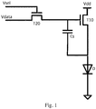
- Fig. 1 is a circuit diagram of a 2T1C pixel driving circuit of related art.
- the 2T1C pixel driving circuit includes a first thin-film transistor (TFT) T10, a second TFT T20, and a capacitor Cs.
- the first TFT T10 is a driving TFT.
- the second TFT T20 is a switch TFT.
- the capacitor Cs is a storage capacitor. Specifically, agate of the second TFT T20 is electrically connected to a scanning signal Vsel. A source of the second TFT T20 is electrically connected to a data signal Vdata. A drain of the second TFT T20 is electrically connected to agate of the first TFT T10.
- a drain of the first TFT T10 is electrically connected to a power signal Vdd.
- a source of the first TFT T10 is electrically connected to an anode node level of the OLED D.
- a cathode of the OLED D is electrically connected to a ground terminal.
- One terminal of the capacitor Cs is electrically connected to a drain of the second TFT T20. The other terminal of the capacitor Cs is electrically connected to the source of the first TFT T10.
- Fig. 2 illustrates a timing diagram of a 2T1C pixel driving circuit as illustrated in Fig. 1 .
- the working process of the 2T1C pixel driving circuit is divided into a first working stage S10 and a second working stage S20.
- the data signal Vdata is a display data signal VDATA
- the scanning signal Vsel is at high voltage level.
- the data signal Vdata is at low voltage level
- the scanning signal Vsel is at low voltage level as well.
- the power signal Vdd is constant high voltage.
- the OLED D gives out light at the second working stage S20.
- the gate-source voltage V gs for driving illumination of the OLED D is irrelevant to the threshold voltage imposed on the first TFT T10. Therefore, the 2T1C pixel driving circuit fails to compensate the threshold voltage imposed on the driving TFT, i.e., the first TFT T10.
- An object of the present disclosure is to propose a pixel driving circuit and an organic light-emitting diode (OLED) display device to effectively compensate for threshold voltage imposed on a driving TFT because of change.
- OLED organic light-emitting diode
- a pixel driving circuit includes a first thin-film transistor (TFT), a second TFT, a third TFT, a fourth TFT, a capacitor, and an organic light-emitting diode (OLED).
- a gate of the first TFT is electrically connected to a first node, a source of the first TFT electrically connected to a second node, and a drain of the first TFT electrically connected to a power signal.
- a gate of the second TFT is electrically connected to a scanning signal, a source of the second TFT is electrically connected to a first reference voltage signal, and a drain of the second TFT is electrically connected to the first node.
- a gate of the third TFT is electrically connected to the scanning signal.
- a source of the third TFT is electrically connected to a drain of the fourth TFT.
- a drain of the third TFT is electrically connected to the second node.
- a gate of the fourth TFT is electrically connected to a data signal, and a source of the fourth is electrically connected to a second reference voltage signal.
- One terminal of the capacitor is electrically connected to the first node.
- the other terminal of the capacitor is electrically connected to the second node.
- An anode of the OLED is electrically connected to the second node.
- a cathode of the OLED is electrically connected to a ground terminal.
- the first reference voltage signal is the power signal.
- a pixel driving circuit includes a first thin-film transistor (TFT), a second TFT, a third TFT, a fourth TFT, a capacitor, and an organic light-emitting diode (OLED).
- a gate of the first TFT is electrically connected to a first node, a source of the first TFT electrically connected to a second node, and a drain of the first TFT electrically connected to a power signal.
- a gate of the second TFT is electrically connected to a scanning signal, a source of the second TFT is electrically connected to a first reference voltage signal, and a drain of the second TFT is electrically connected to the first node.
- a gate of the third TFT is electrically connected to the scanning signal.
- a source of the third TFT is electrically connected to a drain of the fourth TFT.
- a drain of the third TFT is electrically connected to the second node.
- a gate of the fourth TFT is electrically connected to a data signal, and a source of the fourth is electrically connected to a second reference voltage signal.
- One terminal of the capacitor is electrically connected to the first node.
- the other terminal of the capacitor is electrically connected to the second node.
- An anode of the OLED is electrically connected to the second node.
- a cathode of the OLED is electrically connected to a ground terminal.
- an organic light-emitting diode (OLED) display device includes a pixel driving circuit.
- the pixel driving circuit includes a first thin-film transistor (TFT), a second TFT, a third TFT, a fourth TFT, a capacitor, and an organic light-emitting diode (OLED).
- a gate of the first TFT is electrically connected to a first node, a source of the first TFT electrically connected to a second node, and a drain of the first TFT electrically connected to a power signal.
- a gate of the second TFT is electrically connected to a scanning signal, a source of the second TFT is electrically connected to a first reference voltage signal, and a drain of the second TFT is electrically connected to the first node.
- a gate of the third TFT is electrically connected to the scanning signal.
- a source of the third TFT is electrically connected to a drain of the fourth TFT.
- a drain of the third TFT is electrically connected to the second node.
- a gate of the fourth TFT is electrically connected to a data signal, and a source of the fourth is electrically connected to a second reference voltage signal.
- One terminal of the capacitor is electrically connected to the first node.
- the other terminal of the capacitor is electrically connected to the second node.
- An anode of the OLED is electrically connected to the second node.
- a cathode of the OLED is electrically connected to a ground terminal.
- the present disclosure can bring beneficiary effects as describes:
- the fourth TFT is introduced in pixel driving circuit and the OLED display device to control the electric current of the first TFT with the data signal and the second reference signal during the compensation stage of threshold voltage. Further, the compensation voltage of the first TFT (i.e., a driving TFT) is compensated. Because of the introduction of the third TFT, the voltage level of a gate of the first TFT prevents from being affected by the second reference voltage sign during the lighting stage.
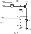
- Fig. 3 is a circuit diagram of a pixel driving circuit according to a first embodiment of the present disclosure.
- the pixel driving circuit 100 includes a first thin-film transistor (TFT) T1, a second TFT T2, a third TFT T3, a fourth TFT T4, a capacitor C1, and an organic light-emitting diode (OLED) D1.
- the first TFT T1 is a driving TFT.
- the second TFT T2 and the third TFT T3 both are switch TFTs.
- the capacitor C1 is a storage capacitor.
- a gate of the first TFT T1 is electrically connected to the first node g.
- a source of the first TFT T1 is electrically connected to the second node s.
- a drain of the first TFT T1 is electrically connected to a power signal Vddl.
- a gate of the second TFT T2 is electrically connected to a scanning signal Vsel1.
- a source of the second TFT T2 is electrically connected to a first reference voltage signal Vref1.
- a drain of the second TFT T2 is electrically connected to the first node g.
- a gate of the third TFT T3 is electrically connected to the scanning signal Vsel1.
- a source of the third TFT T3 is electrically connected to a drain of the fourth TFT T4.
- a drain of the third TFT T3 is electrically connected to the second node s.
- a gate of the fourth TFT T4 is electrically connected to the data signal Vdatal.
- a source of the fourth TFT T4 is electrically connected to a second reference voltage signal Vref2.
- One terminal of the capacitor C1 is electrically connected to the first node g.
- the other terminal of the capacitor C1 is electrically connected to the second node s.
- An anode of the OLED D1 is electrically connected to the second node s.
- a cathode of the OLED D1 is electrically connected to a ground terminal GND.
- a thin-film transistor (TFT) T1 a thin-film transistor (TFT) T1
- a second TFT T2 a third TFT T3, and a fourth TFT T4 all are low temperature poly-silicon (LTPS) TFTs, oxide semiconductor TFTs, or amorphous silicon (a-Si) TFTs.
- LTPS low temperature poly-silicon
- a-Si amorphous silicon
- Fig. 4 illustrates a timing diagram of the pixel driving circuit 100 as illustrated in Fig. 3 .
- the working process of the pixel driving circuit 100 are divided into a compensation stage of threshold voltage S1 and a lighting stage S2.
- the first reference voltage signal Vref1 and the second reference voltage signal Vref2 both are constant low voltage in the working process of the pixel driving circuit 100.
- the first reference voltage signal Vref1 is configured to provide a first reference voltage Va.
- the second reference voltage signal Vref2 is configured to provide a second reference voltage Vb.
- a power signal Vddl is constant high voltage.
- the data signal Vdatal and the scanning signal Vsel1 correspond to the compensation stage of threshold voltage S1 and the lighting stage S2 successively.
- a data signal Vdatal and a scanning signal Vsel1 both are generated through an external timing controller.
- a first reference voltage signal Vref1, a second reference voltage signal Vref2, a power signal Vddl all are generated through a constant voltage source.
- the data signal Vdatal is a display data signal VDATA1 at high voltage level, and the scanning signal Vsel1 is at high voltage level during the compensation stage of threshold voltage S1 so that the first TFT T1, the second TFT T2, the third TFT T3, and the fourth TFT T4 all are turned on.
- the data signal Vdatal writes the display data signal VDATAlat high voltage level into the source of the first TFT T1 through the third TFT T3 and the fourth TFT T4.
- the first reference voltage Va provided by the first reference voltage signal Vref1 is written into the gate of the first TFT T1 through the second TFT T2.
- Vg indicates the voltage level of the first node g (i.e., the voltage level of the gate of the first TFT T1); Vs indicates the voltage level of the second node s (i.e., the voltage level of the source of the first TFT T1); Vgs indicates the voltage across a gate and a source of the first TFT T1; Va indicates a first reference voltage, and Vb indicates a second reference voltage; W L T 4 indicates the ratio of the width to the length of a channel of the fourth TFT T4; W L T 1 indicates the ratio of the width to the length of a channel
- the data signal Vdatal is at low voltage level
- the scanning signal Vsel1 is at low voltage level during the lighting stage S2 so that the first TFT T1 and the fourth TFT T4 are turned on, and the second TFT T2 and the third TFT T3 are disconnected.
- the gate-source voltage V gs imposed on the first TFT T1 remains stable under the function of storage of the capacitor C1.
- the gate-source voltage V gs for driving the OLED D1 to light includes a threshold voltage imposed on the first TFT T10.
- the electric current flowing through the OLED D1 and the square of the difference of the gate-source voltage V gs and the threshold voltage imposed on the first TFT T10 are in direct proportion. Therefore, the electric current flowing through the OLED D1 is irrelevant to the threshold voltage imposed on the first TFT T10, that is, the driving TFT. In other words, the threshold voltage is compensated.
- the gate of the fourth TFT T4 is controlled by the data signal at high voltage levelVDATA1, and the source is controlled by the second reference voltage Vb so the electric current flowing through the first TFT T10 is well controlled by the data signal at high voltage levelVDATA1 and the second reference voltage Vb.
- the third TFT T3 can prevent the second reference voltage Vb from affecting the voltage level of the gate of the first TFT T10.
- the second reference voltage Vb needs to satisfy the following equation: Vb ⁇ VDATA 1 ⁇ Vth 3 ⁇
- the first TFT T1 is turned on normally while the OLED D1 cannot be turned on.
- the first reference voltage Va satisfies the following equation: W L T 4 W L T 1 1 2 VDATA 1 ⁇ Vb ⁇ Vth 3 ⁇ Vth 1 + Voled 1 > Va , and Va > W L T 4 W L T 1 1 2 VDATA 1 ⁇ Vb ⁇ Vth 3 ⁇ Vth 1 ⁇ where Voled1 indicates voltage level of an anode node level of the OLED D1 during the compensation stage of threshold voltage.
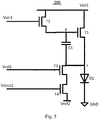
- Fig. 5 is a circuit diagram of a pixel driving circuit 200 according to a second embodiment of the present disclosure.
- the difference between the pixel driving circuit 200 and the pixel driving circuit 100 as Fig. 3 illustrates is that a first reference voltage signal Vref1 is a power signal Vddl in the pixel driving circuit 200.
- a source of the second TFT T2 is directly connected to the power signal Vddl.
- Fig. 6 illustrates a timing diagram of a pixel driving circuit 200 as illustrated in Fig. 5 .
- the difference between the pixel driving circuit 200 and the pixel driving circuit 100 as Fig. 4 illustrates is the working process.
- the power signal Vddl is at reference low voltage level during the compensation stage of threshold voltage S1.
- the reference low voltage level is a first reference voltage Va.
- the power signal Vddl is at high voltage level during the lighting stage S2.
- the power signal Vddl, the data signal Vdatal, and the scanning signal Vsel1 all are generated through an external timing controller in the present embodiment.
- a second reference voltage signal Vref2 is generated through a constant voltage source.
- the voltage level of a gate of the first TFT T1, the voltage level of the source of the first TFT T1, and the gate-source voltage V gs satisfy the equation (1).
- the first reference voltage Va satisfies the equation (3).
- the second reference voltage Vb satisfies the equation (2).
- the first reference voltage Va is the reference low voltage level of the power signal Vddl in the present embodiment.
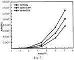
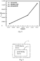
- Fig. 7 illustrates a relationship of the electric current I OLED flowing through the OLED when a drift value ⁇ Vth of the threshold voltage Vth of the conventional 2T1C driving TFT (i.e., the first TFT T10) and a drift value ⁇ Voled of the threshold voltage Vth1 of the first TFT T1 are0 volts, +0.5V, and -0.5V.
- Fig. 7 illustrates a relationship of the electric current I OLED flowing through the OLED when a drift value ⁇ Vth of the threshold voltage Vth of the conventional 2T1C driving TFT (i.e., the first TFT T10) and a drift value ⁇ Voled of the threshold voltage Vth1 of the first TFT T1 are0 volts, +0.5V, and -0.5V.
- Fig. 7 illustrates a relationship of the electric current I OLED flowing through the OLED when a drift value ⁇ Vth of the threshold voltage Vth of the conventional 2T1C driving TFT (i.e., the first
- FIG. 8 illustrates a relationship of the electric current I OLED flowing through the OLED when a drift value ⁇ Vth of the threshold voltage Vth of the driving TFT (i.e., the first TFT T10) 100 or 200 in the present disclosure and a drift value ⁇ Voled of the threshold voltage Vth1 of the first TFT T1 are0 volts, +0.5V, and -0.5V.
- the variation of the electric current flowing through the OLED in the present disclosure is obviously less than the variation of the electric current flowing through the OLED in the 2T1C driving TFT without any compensation. Therefore, the threshold voltage of the driving TFT can be effectively compensated. Not only lighting stability of the OLED is ensured but also the display brightness of the OLED display panel keeps stable. The threshold voltage does not vary with use time, which means that the display quality is improved.
- Fig. 9 is a schematic diagram of an organic light-emitting diode (OLED) display device 1 according to an embodiment of the present disclosure.
- the OLED display device 1 includes a pixel driving circuit 2.
- the pixel driving circuit 2 is the pixel driving circuit 100 or the pixel driving circuit 200.
- the present disclosure can bring beneficiary effects as describes:
- the fourth TFT is introduced in the pixel driving circuit and the OLED display device to control the electric current of the first TFT with the data signal and the second reference signal during the compensation stage of threshold voltage. Further, the compensation voltage of the first TFT (i.e., a driving TFT) is compensated. Because of the introduction of the third TFT, the voltage level of a gate of the first TFT prevents from being affected by the second reference voltage sign during the lighting stage.
Landscapes
- Engineering & Computer Science (AREA)
- Physics & Mathematics (AREA)
- Computer Hardware Design (AREA)
- General Physics & Mathematics (AREA)
- Theoretical Computer Science (AREA)
- Electroluminescent Light Sources (AREA)
- Control Of El Displays (AREA)
- Control Of Indicators Other Than Cathode Ray Tubes (AREA)
- Devices For Indicating Variable Information By Combining Individual Elements (AREA)
Abstract
Description
- The present disclosure relates to the field of liquid crystal display, and more particularly, to a pixel driving circuit and an organic light-emitting diode (OLED) display device.
- An OLED display device of related art is recognized by the industry to have an extremely developmental potential because the OLED display device has advantages of compactness, simple structure, self-illumination, high brightness, wide viewing angle, short response time, etc.
- The OLED device is an electric current driven device. The electric current flows through the OLED to make the OLED give out light. The brightness of the OLED is determined by the electric current. Most integrated circuits (ICs) of related art merely transmits voltage signals so the pixel driving circuit of the OLED needs to transforming a voltage signal into an electric current signal. The pixel driving circuit of related art is a 2T1C pixel with the structure of two TFTs and one capacitor. With the structure, the pixel driving circuit can transform the voltage into the electric current. However, the pixel driving circuit of related art does not have the function of compensation.
-
Fig. 1 is a circuit diagram of a 2T1C pixel driving circuit of related art. The 2T1C pixel driving circuit includes a first thin-film transistor (TFT) T10, a second TFT T20, and a capacitor Cs. The first TFT T10 is a driving TFT. The second TFT T20 is a switch TFT. The capacitor Cs is a storage capacitor. Specifically, agate of the second TFT T20 is electrically connected to a scanning signal Vsel. A source of the second TFT T20 is electrically connected to a data signal Vdata. A drain of the second TFT T20 is electrically connected to agate of the first TFT T10. A drain of the first TFT T10 is electrically connected to a power signal Vdd. A source of the first TFT T10 is electrically connected to an anode node level of the OLED D. A cathode of the OLED D is electrically connected to a ground terminal. One terminal of the capacitor Cs is electrically connected to a drain of the second TFT T20. The other terminal of the capacitor Cs is electrically connected to the source of the first TFT T10. - Please refer to
Fig. 2 as well.Fig. 2 illustrates a timing diagram of a 2T1C pixel driving circuit as illustrated inFig. 1 . The working process of the 2T1C pixel driving circuit is divided into a first working stage S10 and a second working stage S20. At the first working stage S10, the data signal Vdata is a display data signal VDATA, and the scanning signal Vsel is at high voltage level. At the first working stage S20, the data signal Vdata is at low voltage level, and the scanning signal Vsel is at low voltage level as well. At the first working stage S10 and the second working stage S20, the power signal Vdd is constant high voltage. - In the present embodiment, the OLED D gives out light at the second working stage S20. Meanwhile, a gate-source voltage Vgs imposed on the first TFT T10, which drives the OLED D to light, satisfies the following equation:

- As the equation tells, the gate-source voltage Vgs for driving illumination of the OLED D is irrelevant to the threshold voltage imposed on the first TFT T10. Therefore, the 2T1C pixel driving circuit fails to compensate the threshold voltage imposed on the driving TFT, i.e., the first TFT T10.
- An object of the present disclosure is to propose a pixel driving circuit and an organic light-emitting diode (OLED) display device to effectively compensate for threshold voltage imposed on a driving TFT because of change.
- According to a first aspect of the present disclosure, a pixel driving circuit includes a first thin-film transistor (TFT), a second TFT, a third TFT, a fourth TFT, a capacitor, and an organic light-emitting diode (OLED). A gate of the first TFT is electrically connected to a first node, a source of the first TFT electrically connected to a second node, and a drain of the first TFT electrically connected to a power signal. A gate of the second TFT is electrically connected to a scanning signal, a source of the second TFT is electrically connected to a first reference voltage signal, and a drain of the second TFT is electrically connected to the first node. A gate of the third TFT is electrically connected to the scanning signal. A source of the third TFT is electrically connected to a drain of the fourth TFT. A drain of the third TFT is electrically connected to the second node. A gate of the fourth TFT is electrically connected to a data signal, and a source of the fourth is electrically connected to a second reference voltage signal. One terminal of the capacitor is electrically connected to the first node. The other terminal of the capacitor is electrically connected to the second node. An anode of the OLED is electrically connected to the second node. A cathode of the OLED is electrically connected to a ground terminal. The first reference voltage signal is the power signal. A voltage across a gate and a source of the first TFT satisfies the following equation:


- According to a second aspect of the present disclosure, a pixel driving circuit includes a first thin-film transistor (TFT), a second TFT, a third TFT, a fourth TFT, a capacitor, and an organic light-emitting diode (OLED). A gate of the first TFT is electrically connected to a first node, a source of the first TFT electrically connected to a second node, and a drain of the first TFT electrically connected to a power signal. A gate of the second TFT is electrically connected to a scanning signal, a source of the second TFT is electrically connected to a first reference voltage signal, and a drain of the second TFT is electrically connected to the first node. A gate of the third TFT is electrically connected to the scanning signal. A source of the third TFT is electrically connected to a drain of the fourth TFT. A drain of the third TFT is electrically connected to the second node. A gate of the fourth TFT is electrically connected to a data signal, and a source of the fourth is electrically connected to a second reference voltage signal. One terminal of the capacitor is electrically connected to the first node. The other terminal of the capacitor is electrically connected to the second node. An anode of the OLED is electrically connected to the second node. A cathode of the OLED is electrically connected to a ground terminal.
- According to a third aspect of the present disclosure, an organic light-emitting diode (OLED) display device includes a pixel driving circuit. The pixel driving circuit includes a first thin-film transistor (TFT), a second TFT, a third TFT, a fourth TFT, a capacitor, and an organic light-emitting diode (OLED). A gate of the first TFT is electrically connected to a first node, a source of the first TFT electrically connected to a second node, and a drain of the first TFT electrically connected to a power signal. A gate of the second TFT is electrically connected to a scanning signal, a source of the second TFT is electrically connected to a first reference voltage signal, and a drain of the second TFT is electrically connected to the first node. A gate of the third TFT is electrically connected to the scanning signal. A source of the third TFT is electrically connected to a drain of the fourth TFT. A drain of the third TFT is electrically connected to the second node. A gate of the fourth TFT is electrically connected to a data signal, and a source of the fourth is electrically connected to a second reference voltage signal. One terminal of the capacitor is electrically connected to the first node. The other terminal of the capacitor is electrically connected to the second node. An anode of the OLED is electrically connected to the second node. A cathode of the OLED is electrically connected to a ground terminal.
- The present disclosure can bring beneficiary effects as describes: The fourth TFT is introduced in pixel driving circuit and the OLED display device to control the electric current of the first TFT with the data signal and the second reference signal during the compensation stage of threshold voltage. Further, the compensation voltage of the first TFT (i.e., a driving TFT) is compensated. Because of the introduction of the third TFT, the voltage level of a gate of the first TFT prevents from being affected by the second reference voltage sign during the lighting stage.
-
-
Fig. 1 is a circuit diagram of a conventional 2T1C pixel driving circuit. -
Fig. 2 illustrates a timing diagram of the 2T1C pixel driving circuit as illustrated inFig. 1 . -
Fig. 3 is a circuit diagram of a pixel driving circuit according to a first embodiment of the present disclosure. -
Fig. 4 illustrates a timing diagram of the pixel driving circuit as illustrated inFig. 3 . -
Fig. 5 is a circuit diagram of a pixel driving circuit according to a second embodiment of the present disclosure. -
Fig. 6 illustrates a timing diagram of the pixel driving circuit as illustrated inFig. 5 . -
Fig. 7 illustrates a simulation relationship of the electric current flowing through the OLED when a value of a threshold voltage of a driving TFT in the conventional 2T1C pixel driving circuit shifts. -
Fig. 8 illustrates a simulation relationship of the electric current flowing through the OLED when a value of a threshold voltage of a driving TFT in the present disclosure shifts. -
Fig. 9 is a schematic diagram of an organic light-emitting diode (OLED) display device according to an embodiment of the present disclosure. - The invention is described below in detail with reference to the accompanying drawings, wherein like reference numerals are used to identify like elements illustrated in one or more of the figures thereof, and in which exemplary embodiments of the invention are shown. This invention may, however, be embodied in many different forms and should not be construed as limited to the particular embodiments set forth herein. Rather, these embodiments are provided so that this disclosure will be thorough and complete, and will fully convey the scope of the invention to those skilled in the art. The drawings illustrate embodiments of the invention and, together with the description, serve to explain the principles of the invention.
-
Fig. 3 is a circuit diagram of a pixel driving circuit according to a first embodiment of the present disclosure. Thepixel driving circuit 100 includes a first thin-film transistor (TFT) T1, a second TFT T2, a third TFT T3, a fourth TFT T4, a capacitor C1, and an organic light-emitting diode (OLED) D1. The first TFT T1 is a driving TFT. The second TFT T2 and the third TFT T3 both are switch TFTs. The capacitor C1 is a storage capacitor. - A gate of the first TFT T1 is electrically connected to the first node g. A source of the first TFT T1 is electrically connected to the second node s. A drain of the first TFT T1 is electrically connected to a power signal Vddl. A gate of the second TFT T2 is electrically connected to a scanning signal Vsel1. A source of the second TFT T2 is electrically connected to a first reference voltage signal Vref1. A drain of the second TFT T2 is electrically connected to the first node g. A gate of the third TFT T3 is electrically connected to the scanning signal Vsel1. A source of the third TFT T3 is electrically connected to a drain of the fourth TFT T4. A drain of the third TFT T3 is electrically connected to the second node s. A gate of the fourth TFT T4 is electrically connected to the data signal Vdatal. A source of the fourth TFT T4 is electrically connected to a second reference voltage signal Vref2. One terminal of the capacitor C1 is electrically connected to the first node g. The other terminal of the capacitor C1 is electrically connected to the second node s. An anode of the OLED D1 is electrically connected to the second node s. A cathode of the OLED D1 is electrically connected to a ground terminal GND.
- In another embodiment, a thin-film transistor (TFT) T1, a second TFT T2, a third TFT T3, and a fourth TFT T4 all are low temperature poly-silicon (LTPS) TFTs, oxide semiconductor TFTs, or amorphous silicon (a-Si) TFTs.
-
Fig. 4 illustrates a timing diagram of thepixel driving circuit 100 as illustrated inFig. 3 . AsFig. 4 illustrates, the working process of thepixel driving circuit 100 are divided into a compensation stage of threshold voltage S1 and a lighting stage S2. - The first reference voltage signal Vref1 and the second reference voltage signal Vref2 both are constant low voltage in the working process of the
pixel driving circuit 100. The first reference voltage signal Vref1 is configured to provide a first reference voltage Va. The second reference voltage signal Vref2 is configured to provide a second reference voltage Vb. A power signal Vddl is constant high voltage. The data signal Vdatal and the scanning signal Vsel1 correspond to the compensation stage of threshold voltage S1 and the lighting stage S2 successively. - In another embodiment, a data signal Vdatal and a scanning signal Vsel1 both are generated through an external timing controller. A first reference voltage signal Vref1, a second reference voltage signal Vref2, a power signal Vddl all are generated through a constant voltage source.
- The data signal Vdatal is a display data signal VDATA1 at high voltage level, and the scanning signal Vsel1 is at high voltage level during the compensation stage of threshold voltage S1 so that the first TFT T1, the second TFT T2, the third TFT T3, and the fourth TFT T4 all are turned on. The data signal Vdatal writes the display data signal VDATAlat high voltage level into the source of the first TFT T1 through the third TFT T3 and the fourth TFT T4. The first reference voltage Va provided by the first reference voltage signal Vref1 is written into the gate of the first TFT T1 through the second TFT T2.
- That is, during the compensation stage of threshold voltage S1, equations are as follows:
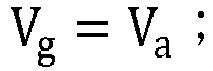


- The data signal Vdatal is at low voltage level, and the scanning signal Vsel1 is at low voltage level during the lighting stage S2 so that the first TFT T1 and the fourth TFT T4 are turned on, and the second TFT T2 and the third TFT T3 are disconnected. The gate-source voltage Vgs imposed on the first TFT T1 remains stable under the function of storage of the capacitor C1.
- The gate-source voltage Vgs for driving the OLED D1 to light includes a threshold voltage imposed on the first TFT T10. The electric current flowing through the OLED D1 and the square of the difference of the gate-source voltage Vgs and the threshold voltage imposed on the first TFT T10 are in direct proportion. Therefore, the electric current flowing through the OLED D1 is irrelevant to the threshold voltage imposed on the first TFT T10, that is, the driving TFT. In other words, the threshold voltage is compensated.
- At the compensation stage of threshold voltage S1 in the present embodiment, the gate of the fourth TFT T4 is controlled by the data signal at high voltage levelVDATA1, and the source is controlled by the second reference voltage Vb so the electric current flowing through the first TFT T10 is well controlled by the data signal at high voltage levelVDATA1 and the second reference voltage Vb. At the lighting stage S2, the third TFT T3 can prevent the second reference voltage Vb from affecting the voltage level of the gate of the first TFT T10.
- In the present embodiment, to ensure the first TFT T1 is turned on normally in the working process of the
pixel driving circuit 100, the second reference voltage Vb needs to satisfy the following equation:
- In the present embodiment, to ensure the first TFT T1 is turned on normally during the compensation stage of threshold voltage S1, the first TFT T1 is turned on normally while the OLED D1 cannot be turned on. The first reference voltage Va satisfies the following equation:

-
Fig. 5 is a circuit diagram of apixel driving circuit 200 according to a second embodiment of the present disclosure. The difference between thepixel driving circuit 200 and thepixel driving circuit 100 asFig. 3 illustrates is that a first reference voltage signal Vref1 is a power signal Vddl in thepixel driving circuit 200. - That is, no first reference signals Vref1 are in the
pixel driving circuit 200. A source of the second TFT T2 is directly connected to the power signal Vddl. - Please refer to
Fig. 6 as well.Fig. 6 illustrates a timing diagram of apixel driving circuit 200 as illustrated inFig. 5 . The difference between thepixel driving circuit 200 and thepixel driving circuit 100 asFig. 4 illustrates is the working process. In thepixel driving circuit 200 asFig. 6 illustrates, the power signal Vddl is at reference low voltage level during the compensation stage of threshold voltage S1. The reference low voltage level is a first reference voltage Va. The power signal Vddl is at high voltage level during the lighting stage S2. - The power signal Vddl, the data signal Vdatal, and the scanning signal Vsel1 all are generated through an external timing controller in the present embodiment. A second reference voltage signal Vref2 is generated through a constant voltage source.
- In the present embodiment, the voltage level of a gate of the first TFT T1, the voltage level of the source of the first TFT T1, and the gate-source voltage Vgs satisfy the equation (1). The first reference voltage Va satisfies the equation (3). The second reference voltage Vb satisfies the equation (2).
- Different from the first embodiment, the first reference voltage Va is the reference low voltage level of the power signal Vddl in the present embodiment.
- Please refer to
Fig. 7 andFig. 8 .Fig. 7 illustrates a relationship of the electric current IOLED flowing through the OLED when a drift value ΔVth of the threshold voltage Vth of the conventional 2T1C driving TFT (i.e., the first TFT T10) and a drift value ΔVoled of the threshold voltage Vth1 of the first TFT T1 are0 volts, +0.5V, and -0.5V.Fig. 8 illustrates a relationship of the electric current IOLED flowing through the OLED when a drift value ΔVth of the threshold voltage Vth of the driving TFT (i.e., the first TFT T10) 100 or 200 in the present disclosure and a drift value ΔVoled of the threshold voltage Vth1 of the first TFT T1 are0 volts, +0.5V, and -0.5V. ComparedFig. 7 andFig. 8 , the variation of the electric current flowing through the OLED in the present disclosure is obviously less than the variation of the electric current flowing through the OLED in the 2T1C driving TFT without any compensation. Therefore, the threshold voltage of the driving TFT can be effectively compensated. Not only lighting stability of the OLED is ensured but also the display brightness of the OLED display panel keeps stable. The threshold voltage does not vary with use time, which means that the display quality is improved. -
Fig. 9 is a schematic diagram of an organic light-emitting diode (OLED)display device 1 according to an embodiment of the present disclosure. TheOLED display device 1 includes apixel driving circuit 2. Thepixel driving circuit 2 is thepixel driving circuit 100 or thepixel driving circuit 200. - The present disclosure can bring beneficiary effects as describes: The fourth TFT is introduced in the pixel driving circuit and the OLED display device to control the electric current of the first TFT with the data signal and the second reference signal during the compensation stage of threshold voltage. Further, the compensation voltage of the first TFT (i.e., a driving TFT) is compensated. Because of the introduction of the third TFT, the voltage level of a gate of the first TFT prevents from being affected by the second reference voltage sign during the lighting stage.
- The present disclosure is described in detail in accordance with the above contents with the specific preferred examples. However, this present disclosure is not limited to the specific examples. For the ordinary technical personnel of the technical field of the present disclosure, on the premise of keeping the conception of the present disclosure, the technical personnel can also make simple deductions or replacements, and all of which should be considered to belong to the protection scope of the present disclosure.
Claims (20)
- A pixel driving circuit, comprising: a first thin-film transistor, TFT, a second TFT, a third TFT, a fourth TFT, a capacitor, and an organic light-emitting diode, OLED;
wherein a gate of the first TFT is electrically connected to a first node, a source of the first TFT is electrically connected to a second node, and a drain of the first TFT is electrically connected to a power signal;
wherein a gate of the second TFT is electrically connected to a scanning signal, a source of the second TFT is electrically connected to a first reference voltage signal, and a drain of the second TFT is electrically connected to the first node;
wherein a gate of the third TFT is electrically connected to the scanning signal; a source of the third TFT is electrically connected to a drain of the fourth TFT; and a drain of the third TFT is electrically connected to the second node;
wherein a gate of the fourth TFT is electrically connected to a data signal, and a source of the fourth is electrically connected to a second reference voltage signal;
wherein a terminal of the capacitor is electrically connected to the first node, and another terminal of the capacitor is electrically connected to the second node;
wherein an anode of the OLED is electrically connected to the second node, and a cathode of the OLED is electrically connected to a ground terminal;
wherein the first reference voltage signal is the power signal; and
wherein a voltage across the gate and the source of the first TFT satisfies a following equation:


- The pixel driving circuit of claim 1, wherein the second reference voltage signal is a constant low voltage, and a group of the power signal, the data signal, and the scanning signal corresponds to a threshold voltage compensating stage of and a lighting stage;
wherein the power signal is at a reference low voltage level, the data signal is a high voltage level of the display data signal, and the scanning signal is at a high voltage level during the threshold voltage compensating stage; and
wherein the power signal is at the high voltage level, the data signal is at a low voltage level, and the scanning signal is at the low voltage level during the lighting stage. - A pixel driving circuit, comprising: a first thin-film transistor, TFT, a second TFT, a third TFT, a fourth TFT, a capacitor, and an organic light-emitting diode, OLED,
wherein a gate of the first TFT is electrically connected to a first node, a source of the first TFT is electrically connected to a second node, and a drain of the first TFT is electrically connected to a power signal;
wherein a gate of the second TFT is electrically connected to a scanning signal, a source of the second TFT is electrically connected to a first reference voltage signal, and a drain of the second TFT is electrically connected to the first node;
wherein a gate of the third TFT is electrically connected to the scanning signal, a source of the third TFT is electrically connected to a drain of the fourth TFT, and a drain of the third TFT is electrically connected to the second node;
wherein a gate of the fourth TFT is electrically connected to a data signal, and a source of the fourth is electrically connected to a second reference voltage signal;
wherein a terminal of the capacitor is electrically connected to the first node, and another terminal of the capacitor is electrically connected to the second node; and
wherein an anode of the OLED is electrically connected to the second node, and a cathode of the OLED is electrically connected to a ground terminal. - The pixel driving circuit of claim 3, wherein the first reference voltage signal and the second reference voltage signal are constant low voltages, the power signal is a constant high voltage, and a group of the data signal and the scanning signal corresponds to a threshold voltage compensating stage and a lighting stage;
wherein the data signal is a high voltage level of a display data signal, and the scanning signal is at a high voltage level during the threshold voltage compensating stage; and
wherein the data signal is at a low voltage level, and the scanning signal is at the low voltage level during the lighting stage. - The pixel driving circuit of claim 4, wherein the data signal and the scanning signal are generated through an external timing controller.
- The pixel driving circuit of claim 3, wherein the first reference voltage signal is the power signal.
- The pixel driving circuit of claim 6, wherein the second reference voltage signal is a constant low voltage, and a group of the power signal, the data signal, and the scanning signal corresponds to a threshold voltage compensating stage and a lighting stage;
wherein the power signal is at a reference low voltage level, the data signal is a high voltage level of a display data signal, and the scanning signal is a high voltage level during the threshold voltage compensating stage; and
wherein the power signal is at the high voltage level, the data signal is at a low voltage level, and the scanning signal is at the low voltage level during the lighting stage. - The pixel driving circuit of claim 7, wherein the power signal, the data signal, and the scanning signal are generated through an external timing controller.
- The pixel driving circuit of claim 3, wherein a voltage across the gate and the source of the first TFT satisfies a following equation:


- The pixel driving circuit of claim 3, wherein a second reference voltage Vb provided by the second reference voltage signal satisfy a following equation:

- The pixel driving circuit of claim 3, wherein the first TFT, the second TFT, the third TFT, and the fourth TFT are low temperature poly-silicon, LTPS, TFTs, oxide semiconductor TFTs, or amorphous silicon, α-Si, TFTs.
- An organic light-emitting diode, OLED, display device comprising a pixel driving circuit, wherein the pixel driving circuit comprises: a first thin-film transistor, TFT, a second TFT, a third TFT, a fourth TFT, a capacitor, and an OLED;
wherein a gate of the first TFT is electrically connected to a first node, a source of the first TFT is electrically connected to a second node, and a drain of the first TFT is electrically connected to a power signal;
wherein a gate of the second TFT is electrically connected to a scanning signal, a source of the second TFT is electrically connected to a first reference voltage signal, and a drain of the second TFT is electrically connected to the first node;
wherein a gate of the third TFT is electrically connected to the scanning signal, a source of the third TFT is electrically connected to a drain of the fourth TFT, a drain of the third TFT is electrically connected to the second node;
wherein a gate of the fourth TFT is electrically connected to a data signal, and a source of the fourth is electrically connected to a second reference voltage signal;
wherein a terminal of the capacitor is electrically connected to the first node, and another terminal of the capacitor is electrically connected to the second node; and
wherein an anode of the OLED is electrically connected to the second node, and a cathode of the OLED is electrically connected to a ground terminal. - The OLED display device of claim 12, wherein the first reference voltage signal and the second reference voltage signal both are constant low voltage; the power signal is constant high voltage; the data signal and the scanning signal correspond to a compensation stage of threshold voltage and a lighting stage successively;
the data signal is a display data signal at high voltage level, and the scanning signal Vsel1 is at high voltage level during the compensation stage of threshold voltage;
the data signal is at low voltage level; the scanning signal is at low voltage level during the lighting stage. - The OLED display device of claim 13, wherein the data signal and the scanning signal both are generated through an external timing controller.
- The OLED display device of claim 12, wherein the first reference voltage signal is the power signal.
- The OLED display device of claim 15, wherein the second reference voltage signal is constant low voltage; the power signal, the data signal, and the scanning signal correspond to a compensation stage of threshold voltage and a lighting stage.
during the compensation stage of threshold voltage, the power signal is at reference low voltage level; the data signal is the display data signal at high voltage level; the scanning signal is at high voltage level;
during the lighting stage, the power signal is at high voltage level; the data signal is at low voltage level; the scanning signal is at low voltage level. - The OLED display device of claim 16, wherein the power signal, the data signal, and the scanning signal all are generated through an external timing controller.
- The OLED display device of claim 12, wherein a voltage across a gate and a source of the first TFT satisfies the following equation:


- The OLED display device of claim 12, wherein the second reference voltage Vb provided by the second reference signal needs to satisfy the following equation:

- The OLED display device of claim 12, wherein the TFT, the second TFT, the third TFT, and the fourth TFT all are low temperature poly-silicon, LTPS, TFTs, oxide semiconductor TFTs, or amorphous silicon, α-Si, TFTs.
Applications Claiming Priority (2)
| Application Number | Priority Date | Filing Date | Title |
|---|---|---|---|
| CN201710156977.6A CN106782340B (en) | 2017-03-16 | 2017-03-16 | A kind of pixel-driving circuit and OLED display |
| PCT/CN2017/081248 WO2018166037A1 (en) | 2017-03-16 | 2017-04-20 | Pixel driving circuit and oled display device |
Publications (2)
| Publication Number | Publication Date |
|---|---|
| EP3598427A1 true EP3598427A1 (en) | 2020-01-22 |
| EP3598427A4 EP3598427A4 (en) | 2020-11-25 |
Family
ID=58966921
Family Applications (1)
| Application Number | Title | Priority Date | Filing Date |
|---|---|---|---|
| EP17900438.7A Withdrawn EP3598427A4 (en) | 2017-03-16 | 2017-04-20 | PIXEL DRIVER CIRCUIT AND OLED DISPLAY DEVICE |
Country Status (6)
| Country | Link |
|---|---|
| US (1) | US10347658B2 (en) |
| EP (1) | EP3598427A4 (en) |
| JP (1) | JP6911276B2 (en) |
| KR (1) | KR20190129948A (en) |
| CN (1) | CN106782340B (en) |
| WO (1) | WO2018166037A1 (en) |
Families Citing this family (10)
| Publication number | Priority date | Publication date | Assignee | Title |
|---|---|---|---|---|
| CN107393466B (en) * | 2017-08-14 | 2019-01-15 | 深圳市华星光电半导体显示技术有限公司 | The OLED external compensation circuit of depletion type TFT |
| CN107507568B (en) | 2017-08-24 | 2019-08-13 | 深圳市华星光电半导体显示技术有限公司 | An OLED pixel circuit and a method for slowing down the aging of an OLED device |
| CN110060627B (en) * | 2019-04-08 | 2020-11-10 | 深圳市华星光电半导体显示技术有限公司 | Pixel driving circuit and display panel |
| CN111833817B (en) * | 2019-04-22 | 2021-10-08 | 成都辰显光电有限公司 | Pixel driving circuit, driving method and display panel |
| CN110706599B (en) * | 2019-10-25 | 2022-01-25 | Tcl华星光电技术有限公司 | Display panel and display device |
| CN111063305A (en) * | 2020-01-07 | 2020-04-24 | 深圳市华星光电半导体显示技术有限公司 | Pixel circuit, display panel and compensation method of pixel circuit reference voltage |
| CN112289266B (en) * | 2020-10-30 | 2021-11-16 | 维沃移动通信有限公司 | Pixel compensation circuit, display device and pixel compensation method |
| WO2022226733A1 (en) | 2021-04-26 | 2022-11-03 | 京东方科技集团股份有限公司 | Pixel circuit, pixel driving method and display device |
| TWI826107B (en) * | 2022-11-09 | 2023-12-11 | 友達光電股份有限公司 | Pixel circuit and driving method thereof |
| CN118379961B (en) * | 2024-05-24 | 2024-10-15 | 国鲸合创(青岛)科技有限公司 | Active organic light emitting display external compensation circuit and method |
Family Cites Families (17)
| Publication number | Priority date | Publication date | Assignee | Title |
|---|---|---|---|---|
| JP2004361753A (en) * | 2003-06-05 | 2004-12-24 | Chi Mei Electronics Corp | Image display device |
| JP4747552B2 (en) * | 2004-10-19 | 2011-08-17 | セイコーエプソン株式会社 | Electro-optical device, electronic apparatus and method |
| JP2008521033A (en) * | 2004-11-16 | 2008-06-19 | イグニス・イノベイション・インコーポレーテッド | System and driving method for active matrix light emitting device display |
| CA2495726A1 (en) * | 2005-01-28 | 2006-07-28 | Ignis Innovation Inc. | Locally referenced voltage programmed pixel for amoled displays |
| TWI485681B (en) * | 2005-08-12 | 2015-05-21 | 半導體能源研究所股份有限公司 | Display device |
| JP5240542B2 (en) * | 2006-09-25 | 2013-07-17 | カシオ計算機株式会社 | Display driving device and driving method thereof, and display device and driving method thereof |
| JP4222426B2 (en) | 2006-09-26 | 2009-02-12 | カシオ計算機株式会社 | Display driving device and driving method thereof, and display device and driving method thereof |
| JP5240544B2 (en) * | 2007-03-30 | 2013-07-17 | カシオ計算機株式会社 | Display device and driving method thereof, display driving device and driving method thereof |
| TWI421834B (en) * | 2009-10-26 | 2014-01-01 | Ind Tech Res Inst | Driving method for oled display panel |
| JP5627694B2 (en) * | 2010-09-06 | 2014-11-19 | パナソニック株式会社 | Display device |
| KR101985933B1 (en) * | 2011-11-15 | 2019-10-01 | 엘지디스플레이 주식회사 | Organic light emitting diode display device |
| CN103544917B (en) * | 2013-07-08 | 2016-01-06 | 京东方科技集团股份有限公司 | Light-emitting diode pixel element circuit, its driving method and display panel |
| US9231063B2 (en) * | 2014-02-24 | 2016-01-05 | International Business Machines Corporation | Boron rich nitride cap for total ionizing dose mitigation in SOI devices |
| CN104167177A (en) * | 2014-08-15 | 2014-11-26 | 合肥鑫晟光电科技有限公司 | Pixel circuit, organic electroluminescence display panel and display device |
| CN104680982B (en) * | 2015-03-27 | 2017-03-08 | 深圳市华星光电技术有限公司 | AMOLED pixel-driving circuit and image element driving method |
| CN104835453B (en) | 2015-05-28 | 2017-04-05 | 京东方科技集团股份有限公司 | A kind of image element circuit, driving method and display device |
| CN106205495A (en) * | 2016-09-09 | 2016-12-07 | 深圳市华星光电技术有限公司 | AMOLED pixel-driving circuit and image element driving method |
-
2017
- 2017-03-16 CN CN201710156977.6A patent/CN106782340B/en active Active
- 2017-04-20 JP JP2019550839A patent/JP6911276B2/en active Active
- 2017-04-20 EP EP17900438.7A patent/EP3598427A4/en not_active Withdrawn
- 2017-04-20 KR KR1020197030476A patent/KR20190129948A/en not_active Ceased
- 2017-04-20 WO PCT/CN2017/081248 patent/WO2018166037A1/en not_active Ceased
- 2017-04-20 US US15/533,445 patent/US10347658B2/en active Active
Also Published As
| Publication number | Publication date |
|---|---|
| KR20190129948A (en) | 2019-11-20 |
| JP6911276B2 (en) | 2021-07-28 |
| US10347658B2 (en) | 2019-07-09 |
| CN106782340A (en) | 2017-05-31 |
| WO2018166037A1 (en) | 2018-09-20 |
| CN106782340B (en) | 2018-09-07 |
| US20180269232A1 (en) | 2018-09-20 |
| EP3598427A4 (en) | 2020-11-25 |
| JP2020514821A (en) | 2020-05-21 |
Similar Documents
| Publication | Publication Date | Title |
|---|---|---|
| US11699394B2 (en) | Pixel circuit, driving method thereof and display device | |
| US10347658B2 (en) | Pixel driving circuit and OLED display device that effectively compensate for threshold voltage imposed on a driving TFT | |
| US11455960B2 (en) | Pixel driving circuit and display panel | |
| US10332451B2 (en) | AMOLED pixel driver circuit and pixel driving method | |
| US10157571B2 (en) | Display panel, method for driving the same and display device | |
| US9355595B2 (en) | Pixel unit driving circuit having an erasing transistor and matching transistor, and method thereof | |
| US20210327347A1 (en) | Pixel circuit and driving method thereof, and display panel | |
| EP3723077A1 (en) | Pixel circuit and drive method therefor, and display apparatus | |
| US12183262B2 (en) | Pixel compensation circuit, display panel, and pixel compensation method | |
| US9318540B2 (en) | Light emitting diode pixel unit circuit and display panel | |
| US12008957B2 (en) | Pixel compensation circuit, display panel and display device | |
| US11562699B2 (en) | Display device and method for driving the same | |
| US20170116919A1 (en) | Pixel circuit and driving method thereof, display device | |
| CN110036435A (en) | Pixel circuit, active-matrix organic LED display panel, display equipment and the method for compensating drive transistor threshold voltage | |
| US20190385521A1 (en) | Pixel driving circuit and liquid crystal display device | |
| US20190164500A1 (en) | Oled pixel circuit and method for driving the same, display apparatus | |
| US10565926B2 (en) | OLED pixel circuit and driving method and related display panel and display apparatus | |
| WO2016119304A1 (en) | Amoled pixel drive circuit and pixel drive method | |
| US20130088165A1 (en) | Light-emitting component driving circuit and related pixel circuit and applications using the same | |
| US10204561B2 (en) | Amoled pixel driving circuit and pixel driving method | |
| WO2016119305A1 (en) | Amoled pixel drive circuit and pixel drive method | |
| US20130265215A1 (en) | Light-emitting component driving circuit and related pixel circuit | |
| US10522078B2 (en) | OLED external compensation circuit of a depletion type TFT | |
| CN110349534A (en) | Pixel circuit and its driving method | |
| US20190333446A1 (en) | Pixel driving circuit and driving method thereof display panel and display apparatus |
Legal Events
| Date | Code | Title | Description |
|---|---|---|---|
| STAA | Information on the status of an ep patent application or granted ep patent |
Free format text: STATUS: THE INTERNATIONAL PUBLICATION HAS BEEN MADE |
|
| PUAI | Public reference made under article 153(3) epc to a published international application that has entered the european phase |
Free format text: ORIGINAL CODE: 0009012 |
|
| STAA | Information on the status of an ep patent application or granted ep patent |
Free format text: STATUS: REQUEST FOR EXAMINATION WAS MADE |
|
| 17P | Request for examination filed |
Effective date: 20191011 |
|
| AK | Designated contracting states |
Kind code of ref document: A1 Designated state(s): AL AT BE BG CH CY CZ DE DK EE ES FI FR GB GR HR HU IE IS IT LI LT LU LV MC MK MT NL NO PL PT RO RS SE SI SK SM TR |
|
| AX | Request for extension of the european patent |
Extension state: BA ME |
|
| DAV | Request for validation of the european patent (deleted) | ||
| DAX | Request for extension of the european patent (deleted) | ||
| A4 | Supplementary search report drawn up and despatched |
Effective date: 20201022 |
|
| RIC1 | Information provided on ipc code assigned before grant |
Ipc: G09G 3/3233 20160101AFI20201019BHEP Ipc: G09G 3/325 20160101ALI20201019BHEP Ipc: G09G 3/3291 20160101ALI20201019BHEP |
|
| STAA | Information on the status of an ep patent application or granted ep patent |
Free format text: STATUS: THE APPLICATION IS DEEMED TO BE WITHDRAWN |
|
| 18D | Application deemed to be withdrawn |
Effective date: 20210521 |