EP3597018B1 - Module électronique de contrôle et procédé de fabrication d'un module électronique de contrôle - Google Patents
Module électronique de contrôle et procédé de fabrication d'un module électronique de contrôle Download PDFInfo
- Publication number
- EP3597018B1 EP3597018B1 EP18701449.3A EP18701449A EP3597018B1 EP 3597018 B1 EP3597018 B1 EP 3597018B1 EP 18701449 A EP18701449 A EP 18701449A EP 3597018 B1 EP3597018 B1 EP 3597018B1
- Authority
- EP
- European Patent Office
- Prior art keywords
- circuit board
- sensor unit
- printed circuit
- board element
- subregion
- Prior art date
- Legal status (The legal status is an assumption and is not a legal conclusion. Google has not performed a legal analysis and makes no representation as to the accuracy of the status listed.)
- Active
Links
- 238000004519 manufacturing process Methods 0.000 title claims description 15
- 238000000034 method Methods 0.000 title claims description 11
- 239000000463 material Substances 0.000 claims description 19
- 230000005540 biological transmission Effects 0.000 claims description 9
- 238000007789 sealing Methods 0.000 claims description 4
- 238000005259 measurement Methods 0.000 claims description 3
- 239000011796 hollow space material Substances 0.000 claims 3
- 238000005538 encapsulation Methods 0.000 claims 2
- 229920001169 thermoplastic Polymers 0.000 claims 2
- 239000004416 thermosoftening plastic Substances 0.000 claims 2
- 229920001187 thermosetting polymer Polymers 0.000 claims 1
- 238000004382 potting Methods 0.000 description 10
- 239000003566 sealing material Substances 0.000 description 9
- 239000012815 thermoplastic material Substances 0.000 description 4
- 238000005452 bending Methods 0.000 description 2
- 238000010438 heat treatment Methods 0.000 description 2
- 238000005476 soldering Methods 0.000 description 2
- 238000004026 adhesive bonding Methods 0.000 description 1
- 230000002411 adverse Effects 0.000 description 1
- 230000000694 effects Effects 0.000 description 1
- 238000005516 engineering process Methods 0.000 description 1
- 239000012530 fluid Substances 0.000 description 1
- 238000003801 milling Methods 0.000 description 1
Images
Classifications
-
- H—ELECTRICITY
- H05—ELECTRIC TECHNIQUES NOT OTHERWISE PROVIDED FOR
- H05K—PRINTED CIRCUITS; CASINGS OR CONSTRUCTIONAL DETAILS OF ELECTRIC APPARATUS; MANUFACTURE OF ASSEMBLAGES OF ELECTRICAL COMPONENTS
- H05K5/00—Casings, cabinets or drawers for electric apparatus
- H05K5/0026—Casings, cabinets or drawers for electric apparatus provided with connectors and printed circuit boards [PCB], e.g. automotive electronic control units
- H05K5/0082—Casings, cabinets or drawers for electric apparatus provided with connectors and printed circuit boards [PCB], e.g. automotive electronic control units specially adapted for transmission control units, e.g. gearbox controllers
-
- B—PERFORMING OPERATIONS; TRANSPORTING
- B60—VEHICLES IN GENERAL
- B60K—ARRANGEMENT OR MOUNTING OF PROPULSION UNITS OR OF TRANSMISSIONS IN VEHICLES; ARRANGEMENT OR MOUNTING OF PLURAL DIVERSE PRIME-MOVERS IN VEHICLES; AUXILIARY DRIVES FOR VEHICLES; INSTRUMENTATION OR DASHBOARDS FOR VEHICLES; ARRANGEMENTS IN CONNECTION WITH COOLING, AIR INTAKE, GAS EXHAUST OR FUEL SUPPLY OF PROPULSION UNITS IN VEHICLES
- B60K23/00—Arrangement or mounting of control devices for vehicle transmissions, or parts thereof, not otherwise provided for
-
- G—PHYSICS
- G01—MEASURING; TESTING
- G01D—MEASURING NOT SPECIALLY ADAPTED FOR A SPECIFIC VARIABLE; ARRANGEMENTS FOR MEASURING TWO OR MORE VARIABLES NOT COVERED IN A SINGLE OTHER SUBCLASS; TARIFF METERING APPARATUS; MEASURING OR TESTING NOT OTHERWISE PROVIDED FOR
- G01D11/00—Component parts of measuring arrangements not specially adapted for a specific variable
- G01D11/24—Housings ; Casings for instruments
- G01D11/245—Housings for sensors
-
- H—ELECTRICITY
- H05—ELECTRIC TECHNIQUES NOT OTHERWISE PROVIDED FOR
- H05K—PRINTED CIRCUITS; CASINGS OR CONSTRUCTIONAL DETAILS OF ELECTRIC APPARATUS; MANUFACTURE OF ASSEMBLAGES OF ELECTRICAL COMPONENTS
- H05K1/00—Printed circuits
- H05K1/02—Details
- H05K1/14—Structural association of two or more printed circuits
- H05K1/147—Structural association of two or more printed circuits at least one of the printed circuits being bent or folded, e.g. by using a flexible printed circuit
-
- H—ELECTRICITY
- H05—ELECTRIC TECHNIQUES NOT OTHERWISE PROVIDED FOR
- H05K—PRINTED CIRCUITS; CASINGS OR CONSTRUCTIONAL DETAILS OF ELECTRIC APPARATUS; MANUFACTURE OF ASSEMBLAGES OF ELECTRICAL COMPONENTS
- H05K1/00—Printed circuits
- H05K1/18—Printed circuits structurally associated with non-printed electric components
- H05K1/181—Printed circuits structurally associated with non-printed electric components associated with surface mounted components
-
- H—ELECTRICITY
- H05—ELECTRIC TECHNIQUES NOT OTHERWISE PROVIDED FOR
- H05K—PRINTED CIRCUITS; CASINGS OR CONSTRUCTIONAL DETAILS OF ELECTRIC APPARATUS; MANUFACTURE OF ASSEMBLAGES OF ELECTRICAL COMPONENTS
- H05K1/00—Printed circuits
- H05K1/18—Printed circuits structurally associated with non-printed electric components
- H05K1/189—Printed circuits structurally associated with non-printed electric components characterised by the use of a flexible or folded printed circuit
-
- H—ELECTRICITY
- H05—ELECTRIC TECHNIQUES NOT OTHERWISE PROVIDED FOR
- H05K—PRINTED CIRCUITS; CASINGS OR CONSTRUCTIONAL DETAILS OF ELECTRIC APPARATUS; MANUFACTURE OF ASSEMBLAGES OF ELECTRICAL COMPONENTS
- H05K3/00—Apparatus or processes for manufacturing printed circuits
- H05K3/22—Secondary treatment of printed circuits
- H05K3/28—Applying non-metallic protective coatings
- H05K3/284—Applying non-metallic protective coatings for encapsulating mounted components
-
- H—ELECTRICITY
- H05—ELECTRIC TECHNIQUES NOT OTHERWISE PROVIDED FOR
- H05K—PRINTED CIRCUITS; CASINGS OR CONSTRUCTIONAL DETAILS OF ELECTRIC APPARATUS; MANUFACTURE OF ASSEMBLAGES OF ELECTRICAL COMPONENTS
- H05K3/00—Apparatus or processes for manufacturing printed circuits
- H05K3/30—Assembling printed circuits with electric components, e.g. with resistor
- H05K3/32—Assembling printed circuits with electric components, e.g. with resistor electrically connecting electric components or wires to printed circuits
-
- H—ELECTRICITY
- H05—ELECTRIC TECHNIQUES NOT OTHERWISE PROVIDED FOR
- H05K—PRINTED CIRCUITS; CASINGS OR CONSTRUCTIONAL DETAILS OF ELECTRIC APPARATUS; MANUFACTURE OF ASSEMBLAGES OF ELECTRICAL COMPONENTS
- H05K3/00—Apparatus or processes for manufacturing printed circuits
- H05K3/36—Assembling printed circuits with other printed circuits
- H05K3/361—Assembling flexible printed circuits with other printed circuits
-
- H—ELECTRICITY
- H05—ELECTRIC TECHNIQUES NOT OTHERWISE PROVIDED FOR
- H05K—PRINTED CIRCUITS; CASINGS OR CONSTRUCTIONAL DETAILS OF ELECTRIC APPARATUS; MANUFACTURE OF ASSEMBLAGES OF ELECTRICAL COMPONENTS
- H05K5/00—Casings, cabinets or drawers for electric apparatus
- H05K5/06—Hermetically-sealed casings
- H05K5/065—Hermetically-sealed casings sealed by encapsulation, e.g. waterproof resin forming an integral casing, injection moulding
-
- B—PERFORMING OPERATIONS; TRANSPORTING
- B60—VEHICLES IN GENERAL
- B60R—VEHICLES, VEHICLE FITTINGS, OR VEHICLE PARTS, NOT OTHERWISE PROVIDED FOR
- B60R16/00—Electric or fluid circuits specially adapted for vehicles and not otherwise provided for; Arrangement of elements of electric or fluid circuits specially adapted for vehicles and not otherwise provided for
- B60R16/02—Electric or fluid circuits specially adapted for vehicles and not otherwise provided for; Arrangement of elements of electric or fluid circuits specially adapted for vehicles and not otherwise provided for electric constitutive elements
- B60R16/023—Electric or fluid circuits specially adapted for vehicles and not otherwise provided for; Arrangement of elements of electric or fluid circuits specially adapted for vehicles and not otherwise provided for electric constitutive elements for transmission of signals between vehicle parts or subsystems
- B60R16/0231—Circuits relating to the driving or the functioning of the vehicle
-
- B—PERFORMING OPERATIONS; TRANSPORTING
- B60—VEHICLES IN GENERAL
- B60Y—INDEXING SCHEME RELATING TO ASPECTS CROSS-CUTTING VEHICLE TECHNOLOGY
- B60Y2200/00—Type of vehicle
- B60Y2200/90—Vehicles comprising electric prime movers
-
- F—MECHANICAL ENGINEERING; LIGHTING; HEATING; WEAPONS; BLASTING
- F16—ENGINEERING ELEMENTS AND UNITS; GENERAL MEASURES FOR PRODUCING AND MAINTAINING EFFECTIVE FUNCTIONING OF MACHINES OR INSTALLATIONS; THERMAL INSULATION IN GENERAL
- F16H—GEARING
- F16H57/00—General details of gearing
- F16H2057/0056—Mounting parts arranged in special position or by special sequence, e.g. for keeping particular parts in his position during assembly
-
- F—MECHANICAL ENGINEERING; LIGHTING; HEATING; WEAPONS; BLASTING
- F16—ENGINEERING ELEMENTS AND UNITS; GENERAL MEASURES FOR PRODUCING AND MAINTAINING EFFECTIVE FUNCTIONING OF MACHINES OR INSTALLATIONS; THERMAL INSULATION IN GENERAL
- F16H—GEARING
- F16H57/00—General details of gearing
-
- H—ELECTRICITY
- H05—ELECTRIC TECHNIQUES NOT OTHERWISE PROVIDED FOR
- H05K—PRINTED CIRCUITS; CASINGS OR CONSTRUCTIONAL DETAILS OF ELECTRIC APPARATUS; MANUFACTURE OF ASSEMBLAGES OF ELECTRICAL COMPONENTS
- H05K1/00—Printed circuits
- H05K1/02—Details
- H05K1/0277—Bendability or stretchability details
- H05K1/028—Bending or folding regions of flexible printed circuits
-
- H—ELECTRICITY
- H05—ELECTRIC TECHNIQUES NOT OTHERWISE PROVIDED FOR
- H05K—PRINTED CIRCUITS; CASINGS OR CONSTRUCTIONAL DETAILS OF ELECTRIC APPARATUS; MANUFACTURE OF ASSEMBLAGES OF ELECTRICAL COMPONENTS
- H05K1/00—Printed circuits
- H05K1/02—Details
- H05K1/11—Printed elements for providing electric connections to or between printed circuits
- H05K1/117—Pads along the edge of rigid circuit boards, e.g. for pluggable connectors
-
- H—ELECTRICITY
- H05—ELECTRIC TECHNIQUES NOT OTHERWISE PROVIDED FOR
- H05K—PRINTED CIRCUITS; CASINGS OR CONSTRUCTIONAL DETAILS OF ELECTRIC APPARATUS; MANUFACTURE OF ASSEMBLAGES OF ELECTRICAL COMPONENTS
- H05K2201/00—Indexing scheme relating to printed circuits covered by H05K1/00
- H05K2201/10—Details of components or other objects attached to or integrated in a printed circuit board
- H05K2201/10007—Types of components
- H05K2201/10151—Sensor
-
- H—ELECTRICITY
- H05—ELECTRIC TECHNIQUES NOT OTHERWISE PROVIDED FOR
- H05K—PRINTED CIRCUITS; CASINGS OR CONSTRUCTIONAL DETAILS OF ELECTRIC APPARATUS; MANUFACTURE OF ASSEMBLAGES OF ELECTRICAL COMPONENTS
- H05K2201/00—Indexing scheme relating to printed circuits covered by H05K1/00
- H05K2201/10—Details of components or other objects attached to or integrated in a printed circuit board
- H05K2201/10007—Types of components
- H05K2201/10189—Non-printed connector
-
- H—ELECTRICITY
- H05—ELECTRIC TECHNIQUES NOT OTHERWISE PROVIDED FOR
- H05K—PRINTED CIRCUITS; CASINGS OR CONSTRUCTIONAL DETAILS OF ELECTRIC APPARATUS; MANUFACTURE OF ASSEMBLAGES OF ELECTRICAL COMPONENTS
- H05K2201/00—Indexing scheme relating to printed circuits covered by H05K1/00
- H05K2201/10—Details of components or other objects attached to or integrated in a printed circuit board
- H05K2201/10227—Other objects, e.g. metallic pieces
- H05K2201/10265—Metallic coils or springs, e.g. as part of a connection element
-
- H—ELECTRICITY
- H05—ELECTRIC TECHNIQUES NOT OTHERWISE PROVIDED FOR
- H05K—PRINTED CIRCUITS; CASINGS OR CONSTRUCTIONAL DETAILS OF ELECTRIC APPARATUS; MANUFACTURE OF ASSEMBLAGES OF ELECTRICAL COMPONENTS
- H05K2203/00—Indexing scheme relating to apparatus or processes for manufacturing printed circuits covered by H05K3/00
- H05K2203/13—Moulding and encapsulation; Deposition techniques; Protective layers
- H05K2203/1305—Moulding and encapsulation
- H05K2203/1316—Moulded encapsulation of mounted components
-
- H—ELECTRICITY
- H05—ELECTRIC TECHNIQUES NOT OTHERWISE PROVIDED FOR
- H05K—PRINTED CIRCUITS; CASINGS OR CONSTRUCTIONAL DETAILS OF ELECTRIC APPARATUS; MANUFACTURE OF ASSEMBLAGES OF ELECTRICAL COMPONENTS
- H05K2203/00—Indexing scheme relating to apparatus or processes for manufacturing printed circuits covered by H05K3/00
- H05K2203/13—Moulding and encapsulation; Deposition techniques; Protective layers
- H05K2203/1305—Moulding and encapsulation
- H05K2203/1327—Moulding over PCB locally or completely
-
- H—ELECTRICITY
- H05—ELECTRIC TECHNIQUES NOT OTHERWISE PROVIDED FOR
- H05K—PRINTED CIRCUITS; CASINGS OR CONSTRUCTIONAL DETAILS OF ELECTRIC APPARATUS; MANUFACTURE OF ASSEMBLAGES OF ELECTRICAL COMPONENTS
- H05K3/00—Apparatus or processes for manufacturing printed circuits
- H05K3/22—Secondary treatment of printed circuits
- H05K3/28—Applying non-metallic protective coatings
-
- H—ELECTRICITY
- H05—ELECTRIC TECHNIQUES NOT OTHERWISE PROVIDED FOR
- H05K—PRINTED CIRCUITS; CASINGS OR CONSTRUCTIONAL DETAILS OF ELECTRIC APPARATUS; MANUFACTURE OF ASSEMBLAGES OF ELECTRICAL COMPONENTS
- H05K3/00—Apparatus or processes for manufacturing printed circuits
- H05K3/36—Assembling printed circuits with other printed circuits
- H05K3/361—Assembling flexible printed circuits with other printed circuits
- H05K3/365—Assembling flexible printed circuits with other printed circuits by abutting, i.e. without alloying process
-
- H—ELECTRICITY
- H05—ELECTRIC TECHNIQUES NOT OTHERWISE PROVIDED FOR
- H05K—PRINTED CIRCUITS; CASINGS OR CONSTRUCTIONAL DETAILS OF ELECTRIC APPARATUS; MANUFACTURE OF ASSEMBLAGES OF ELECTRICAL COMPONENTS
- H05K3/00—Apparatus or processes for manufacturing printed circuits
- H05K3/46—Manufacturing multilayer circuits
- H05K3/4688—Composite multilayer circuits, i.e. comprising insulating layers having different properties
- H05K3/4691—Rigid-flexible multilayer circuits comprising rigid and flexible layers, e.g. having in the bending regions only flexible layers
Definitions
- the invention relates to an electronic control module and a method for producing an electronic control module.
- the electronic control modules often include a sensor or a sensor element, by means of which measured values or measurement data are recorded.
- the sensor element can be part of a sensor unit.
- the sensor or the sensor unit must be arranged at predetermined positions or distances relative to the element or object to be measured.
- the position of the control module or a first printed circuit board element of the control module is also often predetermined.
- the sensor or the sensor unit must therefore be arranged at a predetermined distance or at a predetermined height from the first printed circuit board element.
- a sensor unit carrier is typically used, which is attached to the first printed circuit board element.
- the sensor unit is or will be fastened to the sensor unit carrier on a side of the sensor unit carrier which faces away from the first printed circuit board element.
- a cable or a stamped grid is generally used for the electrical connection between the first printed circuit board element and the sensor or the sensor unit.
- the production is very complex, among other things because many different contacting technologies are used.
- a stamped grid as an electrical connection element between the sensor and
- Sensor unit and the first circuit board element complex and expensive tools are required for production.
- the tools cannot be changed quickly, so that the position of the sensor unit cannot easily be changed during the manufacturing process, among other things because other tools are required and the manufacturing process has to be changed over in a complex manner.
- the angle between the sensor or the sensor unit and the printed circuit board element can only be changed with great effort in the manufacturing process.
- the DE 10 2014 205 386 A1 and the DE 10 2014 205 385 A1 each describe an electronic module, in particular for a transmission control unit, according to the prior art.
- Embodiments of the present invention can advantageously enable the distance of the sensor element from the first printed circuit board element and the angle of the sensor element relative to the first printed circuit board element to be changed in a technically simple manner or adapted during production.
- an electronic control module in particular for a transmission, comprising - a first printed circuit board element, - a sensor unit carrier fastened on the first printed circuit board element, with a sensor unit receptacle for receiving a sensor unit, - the sensor unit with a mounted on a second printed circuit board element and sensor element electrically connected to the second printed circuit board element for detecting at least one measured value, the sensor unit being fixed in the sensor unit receptacle, the second printed circuit board element having a flexible area, the flexible area separating a first partial area of the second printed circuit board element from a second partial area of the second printed circuit board element, wherein the first portion has a predetermined angle to the second portion, and the sensor element is electrically connected to the first printed circuit board element by means of the second portion of the second printed circuit board element, the sensor unit carrier having a cavity for receiving an electrical connection portion between the second portion of the second printed circuit board element and the first printed circuit board element, characterized in that the cavity is sealed oil
- One advantage of this is that typically the distance between the sensor unit or the sensor element and the first printed circuit board element can be adjusted or changed in a technically simple manner during the manufacturing process.
- the angle or the orientation between the sensor unit or the sensor element and the first printed circuit board element can usually be changed or adjusted in a technically simple manner during the manufacturing process, since the second printed circuit board element comprises a flexible or semi-flexible or bendable area.
- the sensor unit or the sensor element generally does not have to go through processes for covering electronic components on the first printed circuit board element, but can only be arranged after these processes. Therefore, the sensor unit or the sensor element typically does not have to be designed to be particularly resistant, in particular to heating or heat.
- the length of the second partial area of the second printed circuit board element can generally be adapted to the required connection length between the sensor unit or the sensor unit and the first printed circuit board element. Another advantage of this is that typically the electrical connection area between the second partial area of the second printed circuit board element and the first printed circuit board element is particularly well protected from the environment. In particular, even if the shape of the sensor unit carrier changes, the electrical connection area or the electrical connection is generally not adversely affected, since the material of the sensor unit carrier is at a distance from the electrical connection area.
- a method for producing an electronic control module comprising the following steps: providing a first printed circuit board element; - Providing a sensor unit, wherein the sensor unit comprises a second printed circuit board element which is separated into a first sub-area and a second sub-area by a flexible area, wherein the first sub-area has a predetermined angle to the second sub-area, the sensor unit also having a on the first sub-area sensor element attached to the second printed circuit board element and electrically connected to the second printed circuit board element for detecting at least one measured value, the sensor element being sealed off in an oil-tight manner from the environment by a sealing material; - arranging a sensor unit carrier on the first circuit board element and connecting the sensor unit carrier to the first circuit board element, wherein the sensor unit carrier has a sensor unit receptacle for receiving the sensor unit; and - arranging and fastening the sensor unit in the sensor unit receptacle in such a way that the
- the advantage here is that generally the height or the distance of the sensor or the sensor unit from the first printed circuit board element can be adjusted or changed in a technically simple manner by changing the height of the sensor unit carrier during the manufacturing process.
- the angle between the sensor or the sensor unit and the first printed circuit board element can typically be changed or adjusted in a technically simple manner, since the second printed circuit board element comprises a flexible or semi-flexible or bendable area. Any desired angle between the sensor and the first circuit board element can generally be achieved by bending the flexible or semi-flexible partial area of the second circuit board element (before the oil-tight sealing with sealing material).
- the adjustable length (to the height of the sensor unit carrier) of the second partial area of the second circuit board element typically ensures a secure electrical connection between the sensor or the sensor unit and the first printed circuit board element without additional elements such as cables and/or lead frames.
- Another advantage of this is that the electrical connection or the electrical connection area between the second partial area of the printed circuit board element and the first printed circuit board element is typically protected from the environment in a technically particularly simple manner. In particular, no additional steps and/or additional elements or components are generally required for sealing the cavity and the electrical connection.
- the sensor unit carrier comprises a thermoplastic material, in particular the sensor unit carrier consists of a thermoplastic material.
- the second partial area of the second printed circuit board element is electrically connected to the first printed circuit board element by means of a spring contact connection.
- the sensor element, in particular the sensor unit, and the flexible area of the second printed circuit board element are sealed against the environment in an oil-tight manner by a duroplastic material.
- a duroplastic material As a result, the electrical connection or the electrical connection area between the second partial area of the printed circuit board element and the first printed circuit board element is generally protected from the environment in a technically particularly simple manner.
- the following steps are carried out before the sensor unit is arranged and fastened in the sensor unit receptacle: application of a potting material for oil-tight sealing of electrical components on the first printed circuit board element from the environment; and curing the potting material.
- the advantage of this is that the sensor unit is typically attached to the sensor unit carrier only after the potting material has hardened. As a result, the sensor unit is generally spared the effects of hardening of the potting material or measures to harden the potting material (e.g. heating). Therefore, the sensor unit can generally consist of or comprise an inexpensive material, in particular a material that is heat-sensitive.
- the second partial area of the second printed circuit board element is electrically connected to the first printed circuit board element by means of a spring contact connection.
- a height of the sensor unit carrier is adjusted to a predetermined height by removing a part of the sensor unit carrier.
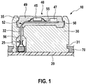
- the electronic control module 10 is, for example, part of a controller for a transmission. It is also conceivable that the control module 10 is used in an electric vehicle.
- the electronic control module 10 comprises a first circuit board element 20.
- the first circuit board element 20 can be a printed-circuit-board (PCB), for example. Electronic components can be arranged on the first circuit board element 20 .
- PCB printed-circuit-board
- At least part of the first circuit board element 20 is covered by a potting material 70 .
- the potting material 70 covers electronic components that are arranged on the first circuit board element 20 and protects them from the environment.
- the potting material 70 is oil-tight so that the electronic components are sealed from an oil environment in which the control module 10 may be located.
- a sensor unit carrier 30 is arranged on the first circuit board element 20 and fastened to the first circuit board element 20 .
- the sensor unit carrier 30 can be fastened to the first circuit board element 20 by means of the potting material 70 which is at least partially present in a (circumferential) lateral recess 31 of the sensor unit carrier 30 provided for this purpose.
- the sensor unit carrier 30 be attached to the first printed circuit board element 20 by soldering (in particular rewflow soldering).
- the position of the sensor unit carrier 30 on the first printed circuit board element 20 can be easily adjusted or changed during the manufacture of the electronic control module 10, since only the position of the electrical connection element (e.g. the spring contact element 25) between the second printed circuit board element 50 and the first printed circuit board element 20 on the first Circuit board element 20 must be changed.
- the electrical connection element e.g. the spring contact element 25
- the sensor unit carrier 30 can include or consist of a thermoplastic material (eg PPS).
- the height (which runs perpendicular to the first circuit board element 20; which in 1 runs from bottom to top) of the sensor unit carrier 30 is changeable. For this purpose, an in 1 Lower portion or area of the sensor unit carrier 30 are removed before arranging the sensor unit carrier 30 on the first circuit board element 20, for example, be cut off or milled.
- the sensor unit carrier 30 lies flat on the first circuit board element 20 .
- the sensor unit carrier 30 has a sensor unit receptacle 35 on the side facing away from the first circuit board element 20 .
- the sensor unit receptacle 35 can comprise or be a recess, for example.
- a sensor unit 40 is arranged in the sensor unit receptacle 35 and fastened to the sensor unit carrier 30 .
- the attachment can be achieved by gluing and/or plugging.
- the sensor unit 40 can be arranged and fixed after the application and curing of the potting material 70 .
- the sensor unit 40 has a second circuit board element 50 .
- the second printed circuit board element 50 can be a printed circuit board, for example.
- a sensor element 45 for detecting at least one measured value (eg a number of revolutions) and possibly other electronic components 47 are arranged and fastened on the second printed circuit board element 50 .
- the sensor element 45 and the additional electronic components 47 that may be present are surrounded by a sealing material 49, so that the sensor element 45 and the additional electronic components 47 are protected from the environment, oil-tight, in particular transmission oil-tight (tight with respect to automatic transmission fluid), are sealed.
- the sealing material 49 can in particular comprise or be a duroplastic material.
- the second printed circuit board element 50 has a flexible or semi-flexible bendable portion or area 52, which divides the second printed circuit board element 50 into a first portion 55 (in 1 running from top to bottom) and a second portion 56 (in 1 running from left to right) separates or divides.
- the flexible area 52 of the second circuit board element 50 can be formed in particular by removing part of the second circuit board element 50 .
- part of the second circuit board element 50 is removed at least on a first side of the second circuit board element 50 .
- the second circuit board element 50 is, so to speak, thinned in the flexible area 52 .
- part of the second circuit board element 50 can also be removed on a second side of the circuit board element 50 opposite the first side of the second circuit board element 50 . This can be done, for example, by milling.
- the second circuit board element 50 is flexible in the flexible area 52 .
- the maximum angle that can be reached between the first partial area 55 and the second partial area 56 can be, for example, approximately 120° or approximately 150°
- the length of the second partial area 56 of the second circuit board element 50 can be adjusted. This is adapted to the height of the sensor unit carrier 30 so that by inserting the second portion 56 of the second circuit board element 50 into the cavity 32 of the sensor unit carrier 30 an electrical connection to the first circuit board element 20 is securely established.
- the bending of the flexible area 52 is carried out before the sensor element 45 and the first portion 55 of the second circuit board element 50 are surrounded with the sealing material 49, ie before the sensor unit 40 is sealed.
- the surrounding can be carried out by overmolding, for example.
- the flexible area 52 is bent in such a way that a predetermined or desired angle between the first partial area 55 of the second circuit board element 50 and the second portion 56 of the second circuit board element 50 is achieved. Since the angle between the second partial area 56 of the second printed circuit board element 50 and the first printed circuit board element 20 is usually approx. 90°, this also sets the angle between the first printed circuit board element 20 and the sensor element 45 or the first partial area 55 of the second printed circuit board element 50.
- the second partial area 56 of the second printed circuit board element 50 can thus always have an angle of approximately 90° to the first printed circuit board element 20. This facilitates the electrical connection between the second circuit board element 50 and the first circuit board element 20.
- the sensor unit carrier 30 can be adapted to the angle between the first section 55 and the second section 56, so that the side of the sensor unit carrier 30 facing away from the first circuit board element 10 runs essentially parallel to the first section 55 of the second circuit board element 50.
- the sensor unit 40 can be adapted to the sensor unit carrier 30 accordingly.
- the sealing material 49 completely surrounds the flexible area 52 of the second circuit board element 50 .
- a part of the second portion 56 of the second circuit board element 50 may be surrounded by the sealing material 49 .
- the second partial area 56 of the second printed circuit board element 50 is free of sealing material 49 .
- An end of the second partial region 56 of the second circuit board element 50 that faces away from the flexible region 52 of the second circuit board element 50 is electrically connected to the first circuit board element 20 via an (SMD) spring contact connection. Since second portion 56 of second printed circuit board element 50 is electrically connected to sensor element 45 via flexible portion 52 of second printed circuit board element 50 and first portion 55 of second printed circuit board element 50, sensor element 45 is thereby electrically connected to first printed circuit board element 20.
- the sensor unit carrier 30 has a cavity 32 which is open to the first circuit board element 20 .
- the second partial area 56 of the second printed circuit board element 50 is inserted into the cavity 32 and, due to the guidance of the sensor unit carrier 30, reaches the spring contact element 25.
- the cavity 32 is sealed in the direction away from the first circuit board element 20 by the sensor unit 40, in particular by the sealing material 49 of the sensor unit 40, oil-tight relative to the environment.
- the cavity 32 and the electrical contact between the second partial area 56 of the second printed circuit board element 50 and the first printed circuit board element 20 are sealed in an oil-tight manner from the environment in a technically simple manner.
Landscapes
- Engineering & Computer Science (AREA)
- Microelectronics & Electronic Packaging (AREA)
- Manufacturing & Machinery (AREA)
- Physics & Mathematics (AREA)
- General Physics & Mathematics (AREA)
- Combustion & Propulsion (AREA)
- Chemical & Material Sciences (AREA)
- Transportation (AREA)
- Mechanical Engineering (AREA)
- Non-Metallic Protective Coatings For Printed Circuits (AREA)
- Control Of Transmission Device (AREA)
- Combinations Of Printed Boards (AREA)
- Structures For Mounting Electric Components On Printed Circuit Boards (AREA)
Claims (8)
- Module de commande électronique (10), en particulier pour une transmission, comprenant- un premier élément de carte de circuits imprimés (20),- un support d'unité de capteur (30) fixé sur le premier élément de carte de circuits imprimés (20), doté d'un logement d'unité de capteur (35) destiné à recevoir une unité de capteur (40),- l'unité de capteur (40) dotée d'un élément de capteur (45) fixé sur un deuxième élément de carte de circuits imprimés (50) et relié électriquement au deuxième élément de carte de circuits imprimés (50), destiné à détecter au moins une valeur de mesure, l'unité de capteur (40) étant fixée dans le logement d'unité de capteur (35), dans lequelle deuxième élément de carte de circuits imprimés (50) présente une zone flexible (52), la zone flexible (52) séparant une première zone partielle (55) du deuxième élément de carte de circuits imprimés (50) par rapport à une deuxième zone partielle (56) du deuxième élément de carte de circuits imprimés (50), la première zone partielle (55) présentant un angle prédéterminé par rapport à la deuxième zone partielle (56), etl'élément de capteur (45) est relié électriquement au premier élément de carte de circuits imprimés (20) au moyen de la deuxième zone partielle (56) du deuxième élément de carte de circuits imprimés (50),le support d'unité de capteur (30) présentant une cavité (32) destinée à recevoir une zone de liaison électrique entre la deuxième zone partielle (56) du deuxième élément de carte de circuits imprimés (50) et le premier élément de carte de circuits imprimés (20),caractérisé en ce que la cavité (32) est rendue étanche à l'huile par rapport à l'environnement par l'unité de capteur (40).
- Module de commande électronique (10) selon la revendication 1, dans lequel le support d'unité de capteur (30) comprend une matière thermoplastique, étant en particulier composé d'une matière thermoplastique.
- Module de commande électronique (10) selon la revendication 1 ou 2, dans lequel la deuxième zone partielle (56) du deuxième élément de carte de circuits imprimés (50) est reliée électriquement au premier élément de carte de circuits imprimés (20) au moyen d'une liaison par contact à ressort (25).
- Module de commande électronique (10) selon l'une quelconque des revendications précédentes, dans lequel l'élément de capteur (45), en particulier l'unité de capteur (40), et la zone flexible (52) du deuxième élément de carte de circuits imprimés (50) sont rendus étanches à l'huile par rapport à l'environnement par un matériau thermodurcissable.
- Procédé de fabrication d'un module de commande électronique (10), en particulier pour une transmission, le procédé comprenant les étapes suivantes consistant à :- prévoir un premier élément de carte de circuits imprimés (20) ;- prévoir une unité de capteur (40), l'unité de capteur (40) présentant un deuxième élément de carte de circuits imprimés (50) qui est séparé par une zone flexible (52) en une première zone partielle (55) et une deuxième zone partielle (56), la première zone partielle (55) présentant un angle prédéterminé par rapport à la deuxième zone partielle (56), l'unité de capteur (40) présentant en outre un élément de capteur (45) fixé sur la première zone partielle (55) du deuxième élément de carte de circuits imprimés (50) et relié électriquement au deuxième élément de carte de circuits imprimés (50), servant à détecter au moins une valeur de mesure, l'élément de capteur (45) étant rendu étanche à l'huile par rapport à l'environnement par un matériau d'étanchéité (49) ;- disposer un support d'unité de capteur (30) sur le premier élément de carte de circuits imprimés (20) et relier le support d'unité de capteur (30) au premier élément de carte de circuits imprimés (20), le support d'unité de capteur (30) présentant un logement d'unité de capteur (35) servant à recevoir l'unité de capteur (40) ; et- disposer et fixer l'unité de capteur (40) dans le logement d'unité de capteur (35) de telle sorte que l'élément de capteur (45) est relié électriquement au premier élément de carte de circuits imprimés (20) au moyen de la deuxième zone partielle (56),l'unité de capteur (40) étant disposée et reliée au support d'unité de capteur (30) de telle sorte qu'une cavité (32) du support d'unité de capteur (30) dans laquelle une liaison électrique de la deuxième zone partielle (56) au premier élément de carte de circuits imprimés (20) est établie, est fermé de manière étanche à l'huile par rapport à l'environnement par l'unité de capteur (40).
- Procédé selon la revendication 5, dans lequel, avant de disposer et fixer l'unité de capteur (40) dans le logement d'unité de capteur (35), les étapes suivantes sont exécutées, consistant à :appliquer un matériau de scellement (70) pour rendre des composants électriques (47) sur le premier élément de carte de circuits imprimés (20) étanches à l'huile par rapport à l'environnement ; etlaisser durcir le matériau (70).
- Procédé selon la revendication 5 ou 6, dans lequel la deuxième zone partielle (56) du deuxième élément de carte de circuits imprimés (50) est reliée électriquement au premier élément de carte de circuits imprimés (20) au moyen d'une liaison par contact à ressort.
- Procédé selon l'une quelconque des revendications 5 à 7, dans lequel une hauteur du support d'unité de capteur (30) est adaptée à une hauteur prédéfinie par enlèvement d'une partie du support d'unité de capteur (30) .
Applications Claiming Priority (2)
| Application Number | Priority Date | Filing Date | Title |
|---|---|---|---|
| DE102017204338.5A DE102017204338A1 (de) | 2017-03-15 | 2017-03-15 | Elektronisches Steuermodul und Verfahren zum Herstellen eines elektronischen Steuermoduls |
| PCT/EP2018/051455 WO2018166679A1 (fr) | 2017-03-15 | 2018-01-22 | Module de commande électronique et procédé de fabrication d'un module de commande électronique |
Publications (2)
| Publication Number | Publication Date |
|---|---|
| EP3597018A1 EP3597018A1 (fr) | 2020-01-22 |
| EP3597018B1 true EP3597018B1 (fr) | 2022-04-06 |
Family
ID=61027722
Family Applications (1)
| Application Number | Title | Priority Date | Filing Date |
|---|---|---|---|
| EP18701449.3A Active EP3597018B1 (fr) | 2017-03-15 | 2018-01-22 | Module électronique de contrôle et procédé de fabrication d'un module électronique de contrôle |
Country Status (5)
| Country | Link |
|---|---|
| US (1) | US11528816B2 (fr) |
| EP (1) | EP3597018B1 (fr) |
| CN (1) | CN110383960B (fr) |
| DE (1) | DE102017204338A1 (fr) |
| WO (1) | WO2018166679A1 (fr) |
Families Citing this family (3)
| Publication number | Priority date | Publication date | Assignee | Title |
|---|---|---|---|---|
| JP6565867B2 (ja) * | 2016-10-28 | 2019-08-28 | 株式会社デンソー | 空気物理量センサ |
| GB201814347D0 (en) * | 2018-09-04 | 2018-10-17 | Pilkington Group Ltd | Electrical device, interlayer ply including an electrical device and methods for making said electrical device and interlayer ply |
| EP3985350A1 (fr) * | 2020-10-13 | 2022-04-20 | Hirt Patent UG (haftungsbeschränkt) | Inclinomètre |
Family Cites Families (12)
| Publication number | Priority date | Publication date | Assignee | Title |
|---|---|---|---|---|
| EP0516149B1 (fr) * | 1991-05-31 | 1998-09-23 | Denso Corporation | Dispositif électronique |
| DE10110948A1 (de) | 2001-03-07 | 2002-09-19 | Siemens Ag | Mechatronische Getriebesteuerung |
| US6913472B2 (en) | 2002-06-28 | 2005-07-05 | Siemens Vdo Automotive Corporation | Method and apparatus for attaching a sensor assembly in a control unit |
| DE102005000655A1 (de) * | 2005-01-04 | 2006-07-13 | Robert Bosch Gmbh | Bilderfassungseinrichtung |
| KR100688989B1 (ko) * | 2005-12-09 | 2007-03-02 | 삼성전기주식회사 | 센서 고정장치 |
| DE102008028977A1 (de) * | 2008-06-18 | 2009-12-24 | Leopold Kostal Gmbh & Co. Kg | Sensoranordnung |
| DE102010026563A1 (de) * | 2010-07-08 | 2012-01-12 | Hella Kgaa Hueck & Co. | Sensoranordnung zur Erfassung von Zustandsgrößen |
| DE102013209296B4 (de) * | 2013-05-21 | 2024-04-18 | Vitesco Technologies GmbH | Elektronisches Modul, insbesondere Steuergerät für ein Fahrzeug |
| DE102013212940A1 (de) * | 2013-06-26 | 2014-12-31 | Zf Friedrichshafen Ag | Sensormodul, Mechatronik-Modul und Verfahren zum Herstellen eines Mechatronik-Moduls |
| DE102014205385A1 (de) | 2014-03-24 | 2015-09-24 | Robert Bosch Gmbh | Elektronikmodul, insbesondere für Getriebesteuergerät, mit zwei übereinander gestapelten Leiterplattenelementen |
| DE102014205386A1 (de) * | 2014-03-24 | 2015-09-24 | Robert Bosch Gmbh | Elektronikmodul, insbesondere für Getriebesteuergerät, mit integriertem elektronischem Sensorelement |
| KR102591365B1 (ko) * | 2016-09-12 | 2023-10-19 | 삼성디스플레이 주식회사 | 확장형 표시 장치 |
-
2017
- 2017-03-15 DE DE102017204338.5A patent/DE102017204338A1/de not_active Withdrawn
-
2018
- 2018-01-22 WO PCT/EP2018/051455 patent/WO2018166679A1/fr unknown
- 2018-01-22 US US16/494,225 patent/US11528816B2/en active Active
- 2018-01-22 CN CN201880017907.5A patent/CN110383960B/zh active Active
- 2018-01-22 EP EP18701449.3A patent/EP3597018B1/fr active Active
Also Published As
| Publication number | Publication date |
|---|---|
| US11528816B2 (en) | 2022-12-13 |
| DE102017204338A1 (de) | 2018-09-20 |
| EP3597018A1 (fr) | 2020-01-22 |
| CN110383960A (zh) | 2019-10-25 |
| WO2018166679A1 (fr) | 2018-09-20 |
| US20200045840A1 (en) | 2020-02-06 |
| CN110383960B (zh) | 2021-06-04 |
Similar Documents
| Publication | Publication Date | Title |
|---|---|---|
| DE19936300B4 (de) | Druckerkennungsvorrichtung und Druckerkennungsvorrichtung-Anordnung hiermit | |
| DE102014118044B4 (de) | Elektronische Steuervorrichtung für ein Kraftfahrzeug unter Verwendung eines Kopplungsgliedes sowie Verfahren zu deren Herstellung | |
| EP3597018B1 (fr) | Module électronique de contrôle et procédé de fabrication d'un module électronique de contrôle | |
| WO2006108534A1 (fr) | Dispositif et procede pour le passage universel de cables | |
| EP2950400B1 (fr) | Câble multi-fils et procédé de fabrication d'un câble multi-fils | |
| DE102014118043B4 (de) | Elektronische Steuervorrichtung für ein Kraftfahrzeug unter Verwendung eines Kopplungsgliedes sowie Verfahren zu deren Herstellung | |
| DE102008036399A1 (de) | Datenkabel | |
| DE102016210532B4 (de) | Sensoranordnung | |
| DE102016006978B4 (de) | Gehäuse | |
| EP3479663B1 (fr) | Unité appareil de commande, en particulier pour un véhicule automobile | |
| DE102013221239B4 (de) | Steuerungseinrichtung | |
| EP3289840B1 (fr) | Module électronique pour appareil de commande de transmission | |
| DE102013215365A1 (de) | Elektrische Getriebesteuervorrichtung und Herstellungsverfahren | |
| EP3555969B1 (fr) | Dispositif de commande de transmission, notamment pour un véhicule à moteur, et procédé de fabrication d'un boîtier de connexion | |
| DE112018005377T5 (de) | Mit einem Anschluss ausgerüsteter Draht | |
| DE102011003239B4 (de) | Sensormodul, Montageelement und Verfahren zum Herstellen eines Sensormoduls | |
| EP3520585B1 (fr) | Procédé de fabrication d'un composant électronique et composant électronique, en particulier pour un module de commande de boîte de vitesses | |
| DE202012012274U1 (de) | Temperaturmessanordnung | |
| EP2509168B1 (fr) | Connecteur à fiche avec aide à l'introduction de contacts | |
| WO2016184679A1 (fr) | Boîtier pour capteur radar, et capteur radar | |
| DE102016210550B4 (de) | Sensorvorrichtung und Verfahren zur Herstellung einer Sensorvorrichtung | |
| DE102014201331A1 (de) | Anordnung zum Verbinden von elektrischen Baugruppen, Verfahren zur Herstellung einer solchen Verbindungsanordnung und Steuergerät | |
| DE102006021560B4 (de) | Umspritzter Flachbandleiter mit heißgeprägter Schaltung | |
| EP3729564A1 (fr) | Connecteur enfichable | |
| EP2980464A1 (fr) | Corps d'étanchéité, procédé de fabrication du corps d'étanchéité et boîtier |
Legal Events
| Date | Code | Title | Description |
|---|---|---|---|
| STAA | Information on the status of an ep patent application or granted ep patent |
Free format text: STATUS: UNKNOWN |
|
| STAA | Information on the status of an ep patent application or granted ep patent |
Free format text: STATUS: THE INTERNATIONAL PUBLICATION HAS BEEN MADE |
|
| PUAI | Public reference made under article 153(3) epc to a published international application that has entered the european phase |
Free format text: ORIGINAL CODE: 0009012 |
|
| STAA | Information on the status of an ep patent application or granted ep patent |
Free format text: STATUS: REQUEST FOR EXAMINATION WAS MADE |
|
| 17P | Request for examination filed |
Effective date: 20191015 |
|
| AK | Designated contracting states |
Kind code of ref document: A1 Designated state(s): AL AT BE BG CH CY CZ DE DK EE ES FI FR GB GR HR HU IE IS IT LI LT LU LV MC MK MT NL NO PL PT RO RS SE SI SK SM TR |
|
| AX | Request for extension of the european patent |
Extension state: BA ME |
|
| RAP1 | Party data changed (applicant data changed or rights of an application transferred) |
Owner name: ROBERT BOSCH GMBH |
|
| DAV | Request for validation of the european patent (deleted) | ||
| DAX | Request for extension of the european patent (deleted) | ||
| GRAP | Despatch of communication of intention to grant a patent |
Free format text: ORIGINAL CODE: EPIDOSNIGR1 |
|
| STAA | Information on the status of an ep patent application or granted ep patent |
Free format text: STATUS: GRANT OF PATENT IS INTENDED |
|
| RIC1 | Information provided on ipc code assigned before grant |
Ipc: F16H 57/00 20120101ALN20211231BHEP Ipc: H05K 3/28 20060101ALN20211231BHEP Ipc: H05K 3/36 20060101ALN20211231BHEP Ipc: H05K 1/11 20060101ALN20211231BHEP Ipc: H05K 3/46 20060101ALN20211231BHEP Ipc: H05K 1/02 20060101ALN20211231BHEP Ipc: G01D 11/24 20060101ALI20211231BHEP Ipc: B60K 23/00 20060101ALI20211231BHEP Ipc: H05K 1/14 20060101ALI20211231BHEP Ipc: H05K 5/00 20060101AFI20211231BHEP |
|
| INTG | Intention to grant announced |
Effective date: 20220127 |
|
| GRAS | Grant fee paid |
Free format text: ORIGINAL CODE: EPIDOSNIGR3 |
|
| GRAA | (expected) grant |
Free format text: ORIGINAL CODE: 0009210 |
|
| STAA | Information on the status of an ep patent application or granted ep patent |
Free format text: STATUS: THE PATENT HAS BEEN GRANTED |
|
| AK | Designated contracting states |
Kind code of ref document: B1 Designated state(s): AL AT BE BG CH CY CZ DE DK EE ES FI FR GB GR HR HU IE IS IT LI LT LU LV MC MK MT NL NO PL PT RO RS SE SI SK SM TR |
|
| REG | Reference to a national code |
Ref country code: GB Ref legal event code: FG4D Free format text: NOT ENGLISH |
|
| REG | Reference to a national code |
Ref country code: CH Ref legal event code: EP |
|
| REG | Reference to a national code |
Ref country code: AT Ref legal event code: REF Ref document number: 1482651 Country of ref document: AT Kind code of ref document: T Effective date: 20220415 |
|
| REG | Reference to a national code |
Ref country code: DE Ref legal event code: R096 Ref document number: 502018009323 Country of ref document: DE |
|
| REG | Reference to a national code |
Ref country code: IE Ref legal event code: FG4D Free format text: LANGUAGE OF EP DOCUMENT: GERMAN |
|
| REG | Reference to a national code |
Ref country code: LT Ref legal event code: MG9D |
|
| REG | Reference to a national code |
Ref country code: NL Ref legal event code: MP Effective date: 20220406 |
|
| PG25 | Lapsed in a contracting state [announced via postgrant information from national office to epo] |
Ref country code: NL Free format text: LAPSE BECAUSE OF FAILURE TO SUBMIT A TRANSLATION OF THE DESCRIPTION OR TO PAY THE FEE WITHIN THE PRESCRIBED TIME-LIMIT Effective date: 20220406 |
|
| PG25 | Lapsed in a contracting state [announced via postgrant information from national office to epo] |
Ref country code: SE Free format text: LAPSE BECAUSE OF FAILURE TO SUBMIT A TRANSLATION OF THE DESCRIPTION OR TO PAY THE FEE WITHIN THE PRESCRIBED TIME-LIMIT Effective date: 20220406 Ref country code: PT Free format text: LAPSE BECAUSE OF FAILURE TO SUBMIT A TRANSLATION OF THE DESCRIPTION OR TO PAY THE FEE WITHIN THE PRESCRIBED TIME-LIMIT Effective date: 20220808 Ref country code: NO Free format text: LAPSE BECAUSE OF FAILURE TO SUBMIT A TRANSLATION OF THE DESCRIPTION OR TO PAY THE FEE WITHIN THE PRESCRIBED TIME-LIMIT Effective date: 20220706 Ref country code: LT Free format text: LAPSE BECAUSE OF FAILURE TO SUBMIT A TRANSLATION OF THE DESCRIPTION OR TO PAY THE FEE WITHIN THE PRESCRIBED TIME-LIMIT Effective date: 20220406 Ref country code: HR Free format text: LAPSE BECAUSE OF FAILURE TO SUBMIT A TRANSLATION OF THE DESCRIPTION OR TO PAY THE FEE WITHIN THE PRESCRIBED TIME-LIMIT Effective date: 20220406 Ref country code: GR Free format text: LAPSE BECAUSE OF FAILURE TO SUBMIT A TRANSLATION OF THE DESCRIPTION OR TO PAY THE FEE WITHIN THE PRESCRIBED TIME-LIMIT Effective date: 20220707 Ref country code: FI Free format text: LAPSE BECAUSE OF FAILURE TO SUBMIT A TRANSLATION OF THE DESCRIPTION OR TO PAY THE FEE WITHIN THE PRESCRIBED TIME-LIMIT Effective date: 20220406 Ref country code: ES Free format text: LAPSE BECAUSE OF FAILURE TO SUBMIT A TRANSLATION OF THE DESCRIPTION OR TO PAY THE FEE WITHIN THE PRESCRIBED TIME-LIMIT Effective date: 20220406 Ref country code: BG Free format text: LAPSE BECAUSE OF FAILURE TO SUBMIT A TRANSLATION OF THE DESCRIPTION OR TO PAY THE FEE WITHIN THE PRESCRIBED TIME-LIMIT Effective date: 20220706 |
|
| PG25 | Lapsed in a contracting state [announced via postgrant information from national office to epo] |
Ref country code: RS Free format text: LAPSE BECAUSE OF FAILURE TO SUBMIT A TRANSLATION OF THE DESCRIPTION OR TO PAY THE FEE WITHIN THE PRESCRIBED TIME-LIMIT Effective date: 20220406 Ref country code: PL Free format text: LAPSE BECAUSE OF FAILURE TO SUBMIT A TRANSLATION OF THE DESCRIPTION OR TO PAY THE FEE WITHIN THE PRESCRIBED TIME-LIMIT Effective date: 20220406 Ref country code: LV Free format text: LAPSE BECAUSE OF FAILURE TO SUBMIT A TRANSLATION OF THE DESCRIPTION OR TO PAY THE FEE WITHIN THE PRESCRIBED TIME-LIMIT Effective date: 20220406 Ref country code: IS Free format text: LAPSE BECAUSE OF FAILURE TO SUBMIT A TRANSLATION OF THE DESCRIPTION OR TO PAY THE FEE WITHIN THE PRESCRIBED TIME-LIMIT Effective date: 20220806 |
|
| REG | Reference to a national code |
Ref country code: DE Ref legal event code: R097 Ref document number: 502018009323 Country of ref document: DE |
|
| PG25 | Lapsed in a contracting state [announced via postgrant information from national office to epo] |
Ref country code: SM Free format text: LAPSE BECAUSE OF FAILURE TO SUBMIT A TRANSLATION OF THE DESCRIPTION OR TO PAY THE FEE WITHIN THE PRESCRIBED TIME-LIMIT Effective date: 20220406 Ref country code: SK Free format text: LAPSE BECAUSE OF FAILURE TO SUBMIT A TRANSLATION OF THE DESCRIPTION OR TO PAY THE FEE WITHIN THE PRESCRIBED TIME-LIMIT Effective date: 20220406 Ref country code: RO Free format text: LAPSE BECAUSE OF FAILURE TO SUBMIT A TRANSLATION OF THE DESCRIPTION OR TO PAY THE FEE WITHIN THE PRESCRIBED TIME-LIMIT Effective date: 20220406 Ref country code: EE Free format text: LAPSE BECAUSE OF FAILURE TO SUBMIT A TRANSLATION OF THE DESCRIPTION OR TO PAY THE FEE WITHIN THE PRESCRIBED TIME-LIMIT Effective date: 20220406 Ref country code: DK Free format text: LAPSE BECAUSE OF FAILURE TO SUBMIT A TRANSLATION OF THE DESCRIPTION OR TO PAY THE FEE WITHIN THE PRESCRIBED TIME-LIMIT Effective date: 20220406 Ref country code: CZ Free format text: LAPSE BECAUSE OF FAILURE TO SUBMIT A TRANSLATION OF THE DESCRIPTION OR TO PAY THE FEE WITHIN THE PRESCRIBED TIME-LIMIT Effective date: 20220406 |
|
| PLBE | No opposition filed within time limit |
Free format text: ORIGINAL CODE: 0009261 |
|
| STAA | Information on the status of an ep patent application or granted ep patent |
Free format text: STATUS: NO OPPOSITION FILED WITHIN TIME LIMIT |
|
| 26N | No opposition filed |
Effective date: 20230110 |
|
| PG25 | Lapsed in a contracting state [announced via postgrant information from national office to epo] |
Ref country code: AL Free format text: LAPSE BECAUSE OF FAILURE TO SUBMIT A TRANSLATION OF THE DESCRIPTION OR TO PAY THE FEE WITHIN THE PRESCRIBED TIME-LIMIT Effective date: 20220406 |
|
| PG25 | Lapsed in a contracting state [announced via postgrant information from national office to epo] |
Ref country code: SI Free format text: LAPSE BECAUSE OF FAILURE TO SUBMIT A TRANSLATION OF THE DESCRIPTION OR TO PAY THE FEE WITHIN THE PRESCRIBED TIME-LIMIT Effective date: 20220406 |
|
| PGFP | Annual fee paid to national office [announced via postgrant information from national office to epo] |
Ref country code: DE Payment date: 20230324 Year of fee payment: 6 |
|
| REG | Reference to a national code |
Ref country code: CH Ref legal event code: PL |
|
| GBPC | Gb: european patent ceased through non-payment of renewal fee |
Effective date: 20230122 |
|
| PG25 | Lapsed in a contracting state [announced via postgrant information from national office to epo] |
Ref country code: LU Free format text: LAPSE BECAUSE OF NON-PAYMENT OF DUE FEES Effective date: 20230122 |
|
| REG | Reference to a national code |
Ref country code: BE Ref legal event code: MM Effective date: 20230131 |
|
| PG25 | Lapsed in a contracting state [announced via postgrant information from national office to epo] |
Ref country code: LI Free format text: LAPSE BECAUSE OF NON-PAYMENT OF DUE FEES Effective date: 20230131 Ref country code: GB Free format text: LAPSE BECAUSE OF NON-PAYMENT OF DUE FEES Effective date: 20230122 Ref country code: CH Free format text: LAPSE BECAUSE OF NON-PAYMENT OF DUE FEES Effective date: 20230131 |
|
| PG25 | Lapsed in a contracting state [announced via postgrant information from national office to epo] |
Ref country code: FR Free format text: LAPSE BECAUSE OF NON-PAYMENT OF DUE FEES Effective date: 20230131 Ref country code: BE Free format text: LAPSE BECAUSE OF NON-PAYMENT OF DUE FEES Effective date: 20230131 |
|
| PG25 | Lapsed in a contracting state [announced via postgrant information from national office to epo] |
Ref country code: IT Free format text: LAPSE BECAUSE OF FAILURE TO SUBMIT A TRANSLATION OF THE DESCRIPTION OR TO PAY THE FEE WITHIN THE PRESCRIBED TIME-LIMIT Effective date: 20220406 Ref country code: IE Free format text: LAPSE BECAUSE OF NON-PAYMENT OF DUE FEES Effective date: 20230122 |
|
| REG | Reference to a national code |
Ref country code: AT Ref legal event code: MM01 Ref document number: 1482651 Country of ref document: AT Kind code of ref document: T Effective date: 20230122 |
|
| PG25 | Lapsed in a contracting state [announced via postgrant information from national office to epo] |
Ref country code: AT Free format text: LAPSE BECAUSE OF NON-PAYMENT OF DUE FEES Effective date: 20230122 |
|
| PG25 | Lapsed in a contracting state [announced via postgrant information from national office to epo] |
Ref country code: AT Free format text: LAPSE BECAUSE OF NON-PAYMENT OF DUE FEES Effective date: 20230122 |