EP3595413B1 - Konstantstrom-led-stromversorgungsschaltung mit maximaler ausgangsleistungsbegrenzungsschaltung - Google Patents
Konstantstrom-led-stromversorgungsschaltung mit maximaler ausgangsleistungsbegrenzungsschaltung Download PDFInfo
- Publication number
- EP3595413B1 EP3595413B1 EP19185437.1A EP19185437A EP3595413B1 EP 3595413 B1 EP3595413 B1 EP 3595413B1 EP 19185437 A EP19185437 A EP 19185437A EP 3595413 B1 EP3595413 B1 EP 3595413B1
- Authority
- EP
- European Patent Office
- Prior art keywords
- resistor
- circuit
- capacitor
- power supply
- constant current
- Prior art date
- Legal status (The legal status is an assumption and is not a legal conclusion. Google has not performed a legal analysis and makes no representation as to the accuracy of the status listed.)
- Active
Links
Images


Classifications
-
- H—ELECTRICITY
- H05—ELECTRIC TECHNIQUES NOT OTHERWISE PROVIDED FOR
- H05B—ELECTRIC HEATING; ELECTRIC LIGHT SOURCES NOT OTHERWISE PROVIDED FOR; CIRCUIT ARRANGEMENTS FOR ELECTRIC LIGHT SOURCES, IN GENERAL
- H05B45/00—Circuit arrangements for operating light-emitting diodes [LED]
- H05B45/30—Driver circuits
- H05B45/37—Converter circuits
- H05B45/3725—Switched mode power supply [SMPS]
- H05B45/385—Switched mode power supply [SMPS] using flyback topology
-
- H—ELECTRICITY
- H05—ELECTRIC TECHNIQUES NOT OTHERWISE PROVIDED FOR
- H05B—ELECTRIC HEATING; ELECTRIC LIGHT SOURCES NOT OTHERWISE PROVIDED FOR; CIRCUIT ARRANGEMENTS FOR ELECTRIC LIGHT SOURCES, IN GENERAL
- H05B45/00—Circuit arrangements for operating light-emitting diodes [LED]
- H05B45/30—Driver circuits
- H05B45/37—Converter circuits
-
- H—ELECTRICITY
- H02—GENERATION; CONVERSION OR DISTRIBUTION OF ELECTRIC POWER
- H02M—APPARATUS FOR CONVERSION BETWEEN AC AND AC, BETWEEN AC AND DC, OR BETWEEN DC AND DC, AND FOR USE WITH MAINS OR SIMILAR POWER SUPPLY SYSTEMS; CONVERSION OF DC OR AC INPUT POWER INTO SURGE OUTPUT POWER; CONTROL OR REGULATION THEREOF
- H02M3/00—Conversion of DC power input into DC power output
- H02M3/22—Conversion of DC power input into DC power output with intermediate conversion into AC
- H02M3/24—Conversion of DC power input into DC power output with intermediate conversion into AC by static converters
- H02M3/28—Conversion of DC power input into DC power output with intermediate conversion into AC by static converters using discharge tubes with control electrode or semiconductor devices with control electrode to produce the intermediate AC
- H02M3/325—Conversion of DC power input into DC power output with intermediate conversion into AC by static converters using discharge tubes with control electrode or semiconductor devices with control electrode to produce the intermediate AC using devices of a triode or a transistor type requiring continuous application of a control signal
- H02M3/335—Conversion of DC power input into DC power output with intermediate conversion into AC by static converters using discharge tubes with control electrode or semiconductor devices with control electrode to produce the intermediate AC using devices of a triode or a transistor type requiring continuous application of a control signal using semiconductor devices only
- H02M3/33507—Conversion of DC power input into DC power output with intermediate conversion into AC by static converters using discharge tubes with control electrode or semiconductor devices with control electrode to produce the intermediate AC using devices of a triode or a transistor type requiring continuous application of a control signal using semiconductor devices only with automatic control of the output voltage or current, e.g. flyback converters
-
- H—ELECTRICITY
- H05—ELECTRIC TECHNIQUES NOT OTHERWISE PROVIDED FOR
- H05B—ELECTRIC HEATING; ELECTRIC LIGHT SOURCES NOT OTHERWISE PROVIDED FOR; CIRCUIT ARRANGEMENTS FOR ELECTRIC LIGHT SOURCES, IN GENERAL
- H05B45/00—Circuit arrangements for operating light-emitting diodes [LED]
- H05B45/30—Driver circuits
- H05B45/34—Voltage stabilisation; Maintaining constant voltage
-
- H—ELECTRICITY
- H05—ELECTRIC TECHNIQUES NOT OTHERWISE PROVIDED FOR
- H05B—ELECTRIC HEATING; ELECTRIC LIGHT SOURCES NOT OTHERWISE PROVIDED FOR; CIRCUIT ARRANGEMENTS FOR ELECTRIC LIGHT SOURCES, IN GENERAL
- H05B45/00—Circuit arrangements for operating light-emitting diodes [LED]
- H05B45/50—Circuit arrangements for operating light-emitting diodes [LED] responsive to malfunctions or undesirable behaviour of LEDs; responsive to LED life; Protective circuits
- H05B45/54—Circuit arrangements for operating light-emitting diodes [LED] responsive to malfunctions or undesirable behaviour of LEDs; responsive to LED life; Protective circuits in a series array of LEDs
-
- H—ELECTRICITY
- H02—GENERATION; CONVERSION OR DISTRIBUTION OF ELECTRIC POWER
- H02M—APPARATUS FOR CONVERSION BETWEEN AC AND AC, BETWEEN AC AND DC, OR BETWEEN DC AND DC, AND FOR USE WITH MAINS OR SIMILAR POWER SUPPLY SYSTEMS; CONVERSION OF DC OR AC INPUT POWER INTO SURGE OUTPUT POWER; CONTROL OR REGULATION THEREOF
- H02M1/00—Details of apparatus for conversion
- H02M1/0003—Details of control, feedback or regulation circuits
- H02M1/0006—Arrangements for supplying an adequate voltage to the control circuit of converters
-
- H—ELECTRICITY
- H05—ELECTRIC TECHNIQUES NOT OTHERWISE PROVIDED FOR
- H05B—ELECTRIC HEATING; ELECTRIC LIGHT SOURCES NOT OTHERWISE PROVIDED FOR; CIRCUIT ARRANGEMENTS FOR ELECTRIC LIGHT SOURCES, IN GENERAL
- H05B45/00—Circuit arrangements for operating light-emitting diodes [LED]
- H05B45/30—Driver circuits
- H05B45/37—Converter circuits
- H05B45/3725—Switched mode power supply [SMPS]
-
- H—ELECTRICITY
- H05—ELECTRIC TECHNIQUES NOT OTHERWISE PROVIDED FOR
- H05B—ELECTRIC HEATING; ELECTRIC LIGHT SOURCES NOT OTHERWISE PROVIDED FOR; CIRCUIT ARRANGEMENTS FOR ELECTRIC LIGHT SOURCES, IN GENERAL
- H05B45/00—Circuit arrangements for operating light-emitting diodes [LED]
- H05B45/30—Driver circuits
- H05B45/37—Converter circuits
- H05B45/3725—Switched mode power supply [SMPS]
- H05B45/382—Switched mode power supply [SMPS] with galvanic isolation between input and output
Definitions
- the present invention relates to LED power supply, with particular emphasis on a constant current LED power supply circuit with maximum output power limiting circuit.
- the circuit structure of the constant current LED power supply on the market mainly adopts the mode of single-stage constant voltage circuit in the front stage and DC-DC step-down circuit in the rear stage.
- the constant current LED power supply adopting this circuit architecture has the characteristics of simple circuit, high cost performance and high efficiency, so that the LED power supply adopting such a circuit structure is relatively popular in the market.
- EP2782238A2 discloses a power supply circuit including a DC-DC converter and an overcurrent protection unit.
- the DC-DC converter converts a first DC voltage into a second DC voltage and supplies the voltage to a DC load.
- the overcurrent protection unit performs feedback control of the DC-DC converter based on current which flows through the DC load.
- the DC-DC converter includes a normally-on type switching element.
- the switching element includes a first electrode, a second electrode, and a third electrode for controlling current which flows between the first electrode and the second electrode, and includes a first state, and a second state where the current which flows between the first electrode and the second electrode is smaller than that of the first state.
- the overcurrent protection unit sets the switching element in the second sate, when the current which flows through the DC load is larger than a reference value.
- US9674908B1 discloses a secondary-side bucking and current-stabilizing flyback power converter adopting a dual-stage isolated circuit architecture and outputting a constant output current to drive a low-power LED module, and its primary stage adopts a flyback circuit architecture with a primary regulated voltage, and its secondary stage adopts of a buck circuit architecture of the current stabilizer, so that after the primary stage converts the constant voltage, the current stabilizer senses the load effect of the output current at the LED module to regulate the output cycle and maintain the total output of the output current constant and reduce the ripple amplitude, so as to achieve a non-strobe output result and improve the illumination effect of the LED module.
- CN107896402A discloses an LED lamp of a constant-current dimming driving circuit based on PWM input.
- the LED lamp comprises a PWM variable power input end, a PWM matching circuit, a voltage rectifying circuit and a DC-DC constant current output circuit and the LED lamp, wherein the voltage signal of the PWM variable power input end is provided by a PWM voltage output power supply, the PWM variable power supply input end is respectively connected with the PWM matching circuit and the voltage rectifying circuit, the PWM matching circuit is connected with the enabling end of the DC-DC constant current output circuit, the voltage rectifying circuit is connected with the power supply end of the DC-DC constant current output circuit, the voltage of the voltage rectifying circuit is changed along with the change of the duty ratio of the voltage of the PWM variable power input end, the voltage of the PWM variable power input end outputs a PWM control signal via divider resistor of the PWM matching circuit, and the PWM control signal passes through the DC-DC constant current output circuit to realize the LED lamp without stroboflash adjustment
- the first technical problem to be solved by the present invention is to provide a maximum output power limiting circuit of constant current LED power supply for the above prior art.
- a second technical problem to be solved by the present invention is to provide a constant current LED power supply circuit for the above prior art.
- the technical solution adopted by the present invention to solve the above first technical problem is a constant current LED power supply circuit according to claim 1.
- the present invention has advantages in that: in the present invention, by adding a voltage stabilizing source circuit for setting DC-DC output current and an output power limiting circuit to an existing constant current LED power supply circuit, the voltage stabilizing source circuit for setting the DC-DC output current is connected to the output end of the single-stage constant voltage power supply circuit, and the output power limiting circuit is connected to the constant current output end of the DC-DC constant current output circuit, thereby utilizing the clamping function between the two diodes of the output power limiting circuit to pull down the voltage of the voltage stabilizing input end of the voltage stabilizing source circuit, and the voltage of the control end D of the DC-DC constant current output circuit also drops in the same proportion, thus, the DC-DC output current corresponding to the DC-DC constant current output circuit is greatly reduced by utilizing the control end D, which limits the output load power.
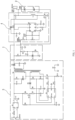
- the maximum output power limiting circuit of constant current LED power supply in the embodiment is used to cooperate with the single-stage constant voltage power supply circuit 3 and the DC-DC constant current output circuit 4 in the constant current LED power supply.
- the maximum output power limiting circuit of constant current LED power supply includes a voltage stabilizing source circuit 1 for setting DC-DC output current and an output power limiting circuit 2; wherein:
- the voltage stabilizing source circuit 1 for setting the DC-DC output current includes a first resistor R1, a second resistor R2, a third resistor R3, a first capacitor C1, a second capacitor C2, and a first voltage stabilizing integrated block D1;
- the first end of the first resistor R1 is connected to the output end of the single-stage constant voltage power supply circuit 3 and the input end of the DC-DC constant current output circuit 4.
- the second end of the first resistor R1 is respectively connected to the first end of the second resistor R2, the first end of the second capacitor C2 and the cathode of the first voltage stabilizing integrated block D1, and the second end of the first resistor R1 is used to connect the voltage stabilizing input end of the DC-DC constant current output circuit 4;
- the first end of the second resistor R2 is connected to the first end of the first capacitor C1, the second end of the second resistor R2 and the second end of the second capacitor C2 are respectively connected to the first end of the third resistor R3;
- the anode of the first voltage stabilizing integrated block D1 and the second end of the third resistor R3 is respectively connected to the internal grounding end of the voltage stabilizing source circuit;
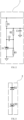
- the output power limiting circuit 2 includes a second diode D2 and a third diode D3; and the third diode D3 is a zener diode; the cathode of the second diode D2 is used to respectively connect the output end of the DC
- the output voltage of the single-stage constant voltage power supply circuit 3 is 55V
- the output voltage of the voltage stabilizing source circuit 1 for setting the DC-DC output current is 25V
- the output power of the DC-DC constant current output circuit 4 is 40W.
- the voltage accuracy of the voltage stabilizing source circuit 1 affects the accuracy of the current outputted by the DC-DC constant current output circuit 4.
- the second diode D2 in the output power limiting circuit 2 belongs to an isolation diode, and the second diode D2 can isolate the voltage at the output end B from flowing into the voltage stabilizing source circuit 1.
- the third diode D3 is a zener diode, and the voltage stabilizing value of the third diode D3 can be set to the maximum output power of the constant current LED power supply.
- the limiting circuit in the embodiment By connecting the limiting circuit in the embodiment to the single-stage constant voltage power supply circuit 3 and the DC-DC constant current output circuit 4 in the constant current LED power supply, the effect of limiting the maximum output power of constant current LED power supply can be achieved.
- the embodiment further provides a constant current LED power supply circuit including a single-stage constant voltage power supply circuit 3 and a DC-DC constant current output circuit 4 and the aforementioned maximum output power limiting circuit of constant current LED power supply, wherein the first end of the first resistor R1 of the limiting circuit is respectively connected to the output end of the single-stage constant voltage power supply circuit 3 and the input end of the DC-DC constant current output circuit 4;
- the second end of the first resistor R1 and the cathode of the third diode D3 are respectively connected to the voltage stabilizing input end of the DC-DC constant current output circuit 4;
- an output end of the DC-DC constant current output circuit 4 ie, the output end A in the figure
- the other output end of the DC-DC constant current output circuit 4 ie, the output end B in the figure
- the embodiment adopts the following technical solutions for the single-stage constant voltage power supply circuit and the DC-DC constant current output circuit:
- the first end of the DC-DC step-down control chip N2 is connected to the cathode of the seventh diode D7, and the second end of the DC-DC step-down control chip N2 is connected to the other end of the sixteenth resistor R16, the fifth end of the DC-DC step-down control chip N2 is connected to one end of the seventh resistor R7, the sixth end of the DC-DC step-down control chip N2 is connected to one end of the thirteenth capacitor C13, and the other end of the thirteenth capacitor C13 is connected to the internal grounding end of the DC-DC constant current output circuit; the other end of the seventeenth resistor R17 is connected to the grid of the third triode Q3, and the source of the third triode Q3 is connected to the internal grounding end of the DC-DC constant current output circuit; One end of the first inductor L1 is connected to one end of the eleventh capacitor C11, and the other end of the first inductor L1 is connected to the drain of the third triode Q3 and the anode of the seventh
- constant current LED power supply circuit other forms of single-stage constant voltage power supply circuit and DC-DC constant current output circuit can also be adopted to realize the functions of the single-stage constant voltage power supply circuit in this embodiment and the functions of the DC-DC constant current output circuit in this embodiment respectively.
- the magnitude of the output current corresponding to the constant current output circuit is set by R16, R14, and R15; the operating frequency of the DC-DC is determined by the first inductor L1 .
- the DC-DC constant current output circuit 4 is a DC-DC conversion circuit.
- the following describes the limitation principle of the limiting circuit on the maximum output power of the constant current LED power supply in the present embodiment with reference to FIG. 1 to FIG. 5 : Assume that the output voltage of the single-stage constant voltage power supply circuit 3 is 55V, the output voltage of the voltage stabilizing source circuit 1 for setting the DC-DC output current is 25V, and the rated output power of the DC-DC constant current output circuit 4 is set to be 40V*1A, that is, the output power is 40W; through the above settings, the voltage at the output end B of the DC-DC constant current output circuit 4 can be made to be about 15V:
- 43.5W here is the maximum output power of the constant current LED power supply, thereby reasonably limiting the output power of the constant current LED power supply. If it is necessary to continue to reduce the maximum output power of the load, it can be achieved by appropriately reducing the voltage stabilizing value of the third diode D3.
Landscapes
- Engineering & Computer Science (AREA)
- Power Engineering (AREA)
- Circuit Arrangement For Electric Light Sources In General (AREA)
- Continuous-Control Power Sources That Use Transistors (AREA)
- Dc-Dc Converters (AREA)
Claims (6)
- Konstantstrom-LED-Stromversorgungsschaltung mit einer Schaltung zur Begrenzung der maximalen Ausgangsleistung, die eine einstufige Konstantspannungs-Stromversorgungsschaltung (3), eine DC-DC-Konstantstrom-Ausgangsschaltung (4) und eine Schaltung zur Begrenzung der maximalen Ausgangsleistung der Konstantstrom-LED-Stromversorgung enthält, die mit der einstufigen Konstantspannungs-Stromversorgungsschaltung (3) und der DC-DC-Konstantstrom-Ausgangsschaltung (4) in der Konstantstrom-LED-Stromversorgung verbunden ist, wobei die Schaltung zur Begrenzung der maximalen Ausgangsleistung der Konstantstrom-LED-Stromversorgung die Spannungsstabilisierungsquellenschaltung (1) zum Einstellen des DC-DC-Ausgangsstroms und eine Ausgangsleistungsbegrenzungsschaltung (2) enthält dadurch gekennzeichnet, dass,
die Ausgangsleistungsbegrenzungsschaltung (2) eine zweite Diode (D2) und eine dritte Diode (D3) enthält; die Kathode der zweiten Diode (D2) verwendet wird, um jeweils ein Ausgangsende der DC-DC-Konstantstrom-Ausgangsschaltung (4) und das Spannungseingangsende der LED-Lampe zu verbinden; die Anode der zweiten Diode (D2) ist mit der Anode der dritten Diode (D3) verbunden, und die Kathode der dritten Diode (D3) ist mit einem ersten Ende eines ersten Kondensators (C1) der Spannungsstabilisierungsquellenschaltung (1) verbunden. - Die Konstantstrom-LED-Stromversorgungsschaltung mit einer Schaltung zur Begrenzung der maximalen Ausgangsleistung nach Anspruch 1, wobei die Spannungsstabilisierungsquellenschaltung (1) zur Einstellung des DC-DC-Ausgangsstroms einen ersten Widerstand (R1), einen zweiten Widerstand (R2), einen dritten Widerstand (R3), den ersten Kondensator (C1), einen zweiten Kondensator (C2) und einen ersten spannungsstabilisierenden integrierten Block (D1) umfasst; das erste Ende des ersten Widerstands (R1) mit dem Ausgangsende der einstufigen Konstantspannungs-Stromversorgungsschaltung (3) und dem Eingangsende der DC-DC-Konstantstrom-Ausgangsschaltung (4) verbunden ist, und das zweite Ende des ersten Widerstands (R1) jeweils mit dem ersten Ende des zweiten Widerstands (R2) verbunden ist, dem ersten Ende des zweiten Kondensators (C2) und der Kathode des ersten spannungsstabilisierenden integrierten Blocks (D1) verbunden ist, und das zweite Ende des ersten Widerstands (R1) verwendet wird, um das spannungsstabilisierende Eingangsende der DC-DC-Konstantstrom-Ausgangsschaltung (4) zu verbinden; das erste Ende des zweiten Widerstands (R2) mit dem ersten Ende des ersten Kondensators (C1) verbunden ist, das zweite Ende des zweiten Widerstands (R2) und das zweite Ende des zweiten Kondensators (C2) jeweils mit dem ersten Ende des dritten Widerstands (R3) verbunden sind; die Anode des ersten spannungsstabilisierenden integrierten Blocks (D1) und das zweite Ende des dritten Widerstands (R3) jeweils mit dem internen Erdungsende der spannungsstabilisierenden Quellenschaltung verbunden ist.
- Die Konstantstrom-LED-Stromversorgungsschaltung mit einer Schaltung zur Begrenzung der maximalen Ausgangsleistung nach Anspruch 1, wobei die dritte Diode (D3) eine Zenerdiode ist.
- Die Konstantstrom-LED-Stromversorgungsschaltung mit einer Schaltung zur Begrenzung der maximalen Ausgangsleistung nach Anspruch 1 oder 2, wobei ein erstes Ende eines ersten Widerstandes (R1) der Begrenzungsschaltung mit dem Ausgangsende der einstufigen Konstantspannungs-Stromversorgungsschaltung (3) bzw. dem Eingangsende der DC-DC-Konstantstrom-Ausgangsschaltung (4) verbunden ist; ein zweites Ende des ersten Widerstands (R1) und die Kathode einer dritten Diode (D3) sind jeweils mit dem spannungsstabilisierenden Eingangsende der DC-DC-Konstantstrom-Ausgangsschaltung (4) verbunden; ein Ausgangsende der DC-DC-Konstantstrom-Ausgangsschaltung (4) mit dem ersten Spannungseingangsende der LED-Lampe verbunden ist und das andere Ausgangsende der DC-DC-Konstantstrom-Ausgangsschaltung (4) jeweils mit der Kathode einer zweiten Diode (D2) und dem zweiten Spannungseingangsende der LED-Lampe in der Begrenzungsschaltung verbunden ist.
- Die Konstantstrom-LED-Stromversorgungsschaltung mit einer Schaltung zur Begrenzung der maximalen Ausgangsleistung nach Anspruch 1 oder 2 oder 4, wobei die einstufige Konstantspannungs-Stromversorgungsschaltung (3) eine Gleichrichterbrücke (B), einen Trenntransformator (TR) und einen Konstantspannungs-Stromversorgungssteuerchip (N1) enthält und das erste Eingangsende der Gleichrichterbrücke (B) über eine Sicherung (F) mit der Feuerleitung (L) der Stromleitung verbunden ist, und das zweite Eingangsende der Gleichrichterbrücke (B) mit der Nullleitung (N) der Stromleitung verbunden ist, und das erste Ausgangsende und das zweite Ausgangsende der Gleichrichterbrücke (B) jeweils an zwei Enden eines dritten Kondensators (C3) angeschlossen sind, und das erste Ausgangsende der Gleichrichterbrücke (B) jeweils mit einem vierten Kondensator (C4), einem vierten Widerstand (R4), einem fünften Widerstand (R5), einem sechsten Widerstand R6 und einem Eingangsende des Isolationstransformators (TR) verbunden ist;das andere Ende des vierten Kondensators (C4) und das andere Ende des vierten Widerstands (R4) jeweils mit der Kathode einer vierten Diode (D4) verbunden sind, und das andere Ende des sechsten Widerstands (R6) mit dem Drain der ersten Triode (Q1) verbunden ist, und das andere Ende des fünften Widerstandes (R5) mit dem Gitter der ersten Triode (Q1) verbunden ist, und das Gitter der ersten Triode (Q1) mit einem Ende des neunten Kondensators (C9) und dem dritten Ende des Konstantspannungs-Stromversorgungs-Steuerchips (N1) verbunden ist, und das andere Ende des neunten Kondensators (C9) geerdet ist; die Anode der vierten Diode (D4) ist mit dem Isolationstransformator (TR) bzw. dem Drain einer zweiten Triode (Q2) verbunden;das erste Ende des Konstantspannungs-Stromversorgungssteuerchips (N1) mit einem sechsten Kondensator (C6), einem siebten Kondensator (C7), einem siebten Widerstand (R7) und einem achten Widerstand (R8) verbunden ist, und das zweite Ende des Konstantspannungs-Stromversorgungssteuerchips (N1) mit einem neunten Widerstand (R9) und einem zehnten Widerstand (R10) verbunden ist, das vierte Ende des Konstantspannungs-Stromversorgungssteuerchips (N1) mit einem zwölften Widerstand (R12) verbunden ist, das fünfte Ende des Konstantspannungs-Stromversorgungssteuerchips (N1) geerdet ist und das sechste Ende des Konstantspannungs-Stromversorgungssteuerchips (N1) mit einem elften Widerstand (R11) verbunden ist; das andere Ende des siebten Widerstands (R7) ist mit der Source der ersten Triode (Q1) verbunden; der achte Widerstand (R8) ist mit der Kathode einer sechsten Diode (D6) verbunden, und der neunte Widerstand (R9) ist mit der Anode der sechsten Diode (D6) verbunden; das andere Ende des elften Widerstands (R11) mit dem Gitter der zweiten Triode (Q2) verbunden ist, und das andere Ende des zwölften Widerstands (R12) mit dem dreizehnten Widerstand (R13) bzw. der Source der zweiten Triode (Q2) verbunden ist, und das andere Ende des dreizehnten Widerstands (R13) geerdet ist;ein Ausgangsende des Isolationstransformators (TR) mit einer Anode einer fünften Diode (D5) verbunden ist, eine Kathode der fünften Diode (D5) mit einem fünften Kondensator (C5) verbunden ist, und das andere Ende des fünften Kondensators (C5) mit dem internen Erdungsende der einstufigen Konstantspannungs-Stromversorgungsschaltung verbunden ist, und ein achter Kondensator (C8) in der einstufigen Konstantspannungs-Stromversorgungsschaltung vorgesehen ist; ein Ende des achten Kondensators (C8) geerdet ist und das andere Ende des achten Kondensators (C8) mit dem internen Erdungsende des einstufigen Konstantspannungs-Stromversorgungskreises verbunden ist.
- Die Konstantstrom-LED-Stromversorgungsschaltung mit einer Schaltung zur Begrenzung der maximalen Ausgangsleistung nach Anspruch 1 oder 2 oder 4, wobei die DC-DC-Konstantstrom-Ausgangsschaltung (4) einen DC-DC-Abwärtssteuerchip (N2), eine dritte Triode (Q3) eine erste Induktivität (L1) und eine siebte Diode (D7), einen zehnten Kondensator (C10), einen zwölften Kondensator (C12), einen dreizehnten Kondensator (C13), einen vierzehnten Widerstand (R14), einen fünfzehnten Widerstand (R15), einen sechzehnten Widerstand (R16) und einen siebzehnten Widerstand (R17);das erste Ende des zehnten Kondensators (C10) mit der Kathode der siebten Diode (D7) und einem Ende des sechzehnten Widerstands (R16) verbunden ist, und dieses erste Ende des zehnten Kondensators (C10) verwendet wird, um den ersten Widerstand (R1) in der Begrenzungsschaltung anzuschließen, und das zweite Ende des zehnten Kondensators (C10) mit dem internen Erdungsende der DC-DC-Konstantstrom-Ausgangsschaltung verbunden ist;ein Ende des vierzehnten Widerstandes (R14) mit dem spannungsstabilisierenden Ausgangsende der spannungsstabilisierenden Quellenschaltung verbunden ist, und das andere Ende des vierzehnten Widerstandes (R14) jeweils mit einem Ende des fünfzehnten Widerstandes (R15), einem Ende des zwölften Kondensators (C12) und dem dritten Ende des DC-DC-Abwärtssteuerchips (N2) verbunden ist; das andere Ende des fünfzehnten Widerstands (R15), das andere Ende des zwölften Kondensators (C12) und das vierte Ende des DC-DC-Abwärtssteuerchips (N2) jeweils mit dem internen Erdungsende der DC-DC-Konstantstrom-Ausgangsschaltung verbunden sind;das erste Ende des DC-DC-Abwärtssteuerchips (N2) mit der Kathode der siebten Diode (D7) verbunden ist, und das zweite Ende des DC-DC-Abwärtssteuerchips (N2) mit dem anderen Ende des sechzehnten Widerstands (R16) verbunden ist, das fünfte Ende des DC-DC-Abwärtssteuerchips (N2) mit einem Ende des siebten Widerstands (R7) verbunden ist, das sechste Ende des DC-DC-Abwärtssteuerchips (N2) mit einem Ende des dreizehnten Kondensators (C13) verbunden ist und das andere Ende des dreizehnten Kondensators (C13) mit dem internen Erdungsende der DC-DC-Konstantstrom-Ausgangsschaltung verbunden ist; das andere Ende des siebzehnten Widerstands (R17) mit dem Gitter der dritten Triode (Q3) verbunden ist und die Source der dritten Triode (Q3) mit der internen Erdungsseite der DC-DC-Konstantstromausgangsschaltung verbunden ist; ein Ende der ersten Induktivität (L1) mit einem Ende des elften Kondensators (C11) verbunden ist und das andere Ende der ersten Induktivität (L1) mit dem Drain der dritten Triode (Q3) bzw. der Anode der siebten Diode (D7) verbunden ist.
Applications Claiming Priority (1)
| Application Number | Priority Date | Filing Date | Title |
|---|---|---|---|
| CN201810751111.4A CN108882450B (zh) | 2018-07-10 | 2018-07-10 | 恒流led电源最高输出功率的限制电路及恒流led电源电路 |
Publications (2)
| Publication Number | Publication Date |
|---|---|
| EP3595413A1 EP3595413A1 (de) | 2020-01-15 |
| EP3595413B1 true EP3595413B1 (de) | 2023-10-18 |
Family
ID=64300615
Family Applications (1)
| Application Number | Title | Priority Date | Filing Date |
|---|---|---|---|
| EP19185437.1A Active EP3595413B1 (de) | 2018-07-10 | 2019-07-10 | Konstantstrom-led-stromversorgungsschaltung mit maximaler ausgangsleistungsbegrenzungsschaltung |
Country Status (2)
| Country | Link |
|---|---|
| EP (1) | EP3595413B1 (de) |
| CN (1) | CN108882450B (de) |
Families Citing this family (8)
| Publication number | Priority date | Publication date | Assignee | Title |
|---|---|---|---|---|
| CN209982783U (zh) * | 2019-03-06 | 2020-01-21 | 厦门赢科光电有限公司 | 一种led驱动电路及驱动装置 |
| CN111491423B (zh) * | 2020-03-27 | 2022-07-05 | 普联技术有限公司 | 单火开关电路及单火开关装置 |
| CA3173764A1 (en) | 2020-04-03 | 2021-10-07 | Myriota Pty Ltd | System and method for adaptive communications |
| CN113301688B (zh) * | 2021-05-10 | 2024-04-12 | 赛尔富电子有限公司 | 可限制电源输出功率和空载电压的恒流led电源电路 |
| CN113709937B (zh) * | 2021-08-20 | 2024-09-20 | 深圳市明微电子股份有限公司 | 一种相对相位的控制电路及led恒流系统 |
| GB2613405A (en) * | 2021-12-02 | 2023-06-07 | Petalite Ltd | A flyback converter |
| CN114415769B (zh) * | 2021-12-09 | 2023-06-02 | 华荣科技股份有限公司 | 一种保护电感快关断的恒流源电路 |
| CN116546341A (zh) * | 2022-01-26 | 2023-08-04 | 陕西智引科技有限公司 | 一种5g矿用本安型无线信号转换器 |
Family Cites Families (5)
| Publication number | Priority date | Publication date | Assignee | Title |
|---|---|---|---|---|
| JP6257022B2 (ja) * | 2013-03-22 | 2018-01-10 | 東芝ライテック株式会社 | 電源回路及び照明装置 |
| CN104580959A (zh) * | 2013-10-25 | 2015-04-29 | 西安群丰电子信息科技有限公司 | 一种led电视电源电路 |
| TWM533373U (en) * | 2016-07-26 | 2016-12-01 | Unity Opto Technology Co Ltd | Flyback power converter with step-down voltage and constant flow at secondary side |
| CN107896402A (zh) * | 2017-12-18 | 2018-04-10 | 赛尔富电子有限公司 | 一种基于pwm输入的恒流调光驱动电路的led灯 |
| CN208572499U (zh) * | 2018-07-10 | 2019-03-01 | 赛尔富电子有限公司 | 恒流led电源最高输出功率的限制电路及恒流led电源电路 |
-
2018
- 2018-07-10 CN CN201810751111.4A patent/CN108882450B/zh active Active
-
2019
- 2019-07-10 EP EP19185437.1A patent/EP3595413B1/de active Active
Also Published As
| Publication number | Publication date |
|---|---|
| CN108882450B (zh) | 2023-08-01 |
| EP3595413A1 (de) | 2020-01-15 |
| CN108882450A (zh) | 2018-11-23 |
Similar Documents
| Publication | Publication Date | Title |
|---|---|---|
| EP3595413A1 (de) | Konstantstrom-led-stromversorgungsschaltung mit maximaler ausgangsleistungsbegrenzungsschaltung | |
| CN106488607B (zh) | 开关电源及电视机 | |
| CN105322803B (zh) | 恒压恒流同步输出电源及电视机 | |
| CN102474189B (zh) | 低成本电源电路和方法 | |
| CN106793293B (zh) | 调光装置及led调光驱动电源 | |
| CN104253960B (zh) | 一种低功耗的稳压背光控制电路和电视机 | |
| WO2021249332A1 (zh) | 一种电荷泵控制电路及驱动电源 | |
| CN108336815A (zh) | 供电装置和车用控制器备用电源 | |
| CN103944416A (zh) | 一种电路简单的多输出开关直流稳压电源 | |
| JP2015053225A (ja) | Led駆動回路 | |
| CN104124862A (zh) | 无需环路补偿的高pfc恒流控制装置及电压变换器 | |
| CN105958825B (zh) | 一种原边电流控制驱动电路 | |
| CN110247563A (zh) | 交流-直流转换电路和方法以及充电器 | |
| CN112383220A (zh) | 控制电路以及应用其的开关变换器 | |
| CN217240990U (zh) | Led驱动电路及led照明装置 | |
| CN113394983B (zh) | 一种反激式变换器的电压反馈电路及其控制方法 | |
| CN115002971A (zh) | Led驱动电路及led照明装置 | |
| CN112117899B (zh) | 一种电流模式控制的boost转换器 | |
| CN106655749B (zh) | 一种电源控制电路及应用其的开关电源 | |
| CN110391749A (zh) | 一种高电压宽输入开关电源 | |
| CN208572499U (zh) | 恒流led电源最高输出功率的限制电路及恒流led电源电路 | |
| CN107820347A (zh) | 一种驱动电源和照明装置 | |
| WO2021248266A1 (en) | Ripple suppression circuit, controlling method and driving equipment | |
| CN206412069U (zh) | 一种反馈保护电路和背光电源电路 | |
| CN210113708U (zh) | 一种交流输入电压转换电路 |
Legal Events
| Date | Code | Title | Description |
|---|---|---|---|
| PUAI | Public reference made under article 153(3) epc to a published international application that has entered the european phase |
Free format text: ORIGINAL CODE: 0009012 |
|
| STAA | Information on the status of an ep patent application or granted ep patent |
Free format text: STATUS: THE APPLICATION HAS BEEN PUBLISHED |
|
| AK | Designated contracting states |
Kind code of ref document: A1 Designated state(s): AL AT BE BG CH CY CZ DE DK EE ES FI FR GB GR HR HU IE IS IT LI LT LU LV MC MK MT NL NO PL PT RO RS SE SI SK SM TR |
|
| AX | Request for extension of the european patent |
Extension state: BA ME |
|
| STAA | Information on the status of an ep patent application or granted ep patent |
Free format text: STATUS: REQUEST FOR EXAMINATION WAS MADE |
|
| 17P | Request for examination filed |
Effective date: 20200713 |
|
| RBV | Designated contracting states (corrected) |
Designated state(s): AL AT BE BG CH CY CZ DE DK EE ES FI FR GB GR HR HU IE IS IT LI LT LU LV MC MK MT NL NO PL PT RO RS SE SI SK SM TR |
|
| STAA | Information on the status of an ep patent application or granted ep patent |
Free format text: STATUS: EXAMINATION IS IN PROGRESS |
|
| 17Q | First examination report despatched |
Effective date: 20210728 |
|
| REG | Reference to a national code |
Ref country code: DE Ref legal event code: R079 Free format text: PREVIOUS MAIN CLASS: H05B0033080000 Ipc: H02M0001320000 Ref document number: 602019039479 Country of ref document: DE |
|
| GRAP | Despatch of communication of intention to grant a patent |
Free format text: ORIGINAL CODE: EPIDOSNIGR1 |
|
| STAA | Information on the status of an ep patent application or granted ep patent |
Free format text: STATUS: GRANT OF PATENT IS INTENDED |
|
| RIC1 | Information provided on ipc code assigned before grant |
Ipc: H02M 1/32 20070101AFI20230628BHEP |
|
| INTG | Intention to grant announced |
Effective date: 20230713 |
|
| RAP3 | Party data changed (applicant data changed or rights of an application transferred) |
Owner name: LIN, WANJIONG Owner name: SELF ELECTRONICS GERMANY GMBH Owner name: SELF ELECTRONICS CO., LTD. |
|
| GRAS | Grant fee paid |
Free format text: ORIGINAL CODE: EPIDOSNIGR3 |
|
| GRAA | (expected) grant |
Free format text: ORIGINAL CODE: 0009210 |
|
| STAA | Information on the status of an ep patent application or granted ep patent |
Free format text: STATUS: THE PATENT HAS BEEN GRANTED |
|
| AK | Designated contracting states |
Kind code of ref document: B1 Designated state(s): AL AT BE BG CH CY CZ DE DK EE ES FI FR GB GR HR HU IE IS IT LI LT LU LV MC MK MT NL NO PL PT RO RS SE SI SK SM TR |
|
| REG | Reference to a national code |
Ref country code: GB Ref legal event code: FG4D |
|
| REG | Reference to a national code |
Ref country code: CH Ref legal event code: EP |
|
| REG | Reference to a national code |
Ref country code: IE Ref legal event code: FG4D |
|
| REG | Reference to a national code |
Ref country code: DE Ref legal event code: R096 Ref document number: 602019039479 Country of ref document: DE |
|
| REG | Reference to a national code |
Ref country code: LT Ref legal event code: MG9D |
|
| REG | Reference to a national code |
Ref country code: NL Ref legal event code: MP Effective date: 20231018 |
|
| REG | Reference to a national code |
Ref country code: AT Ref legal event code: MK05 Ref document number: 1623354 Country of ref document: AT Kind code of ref document: T Effective date: 20231018 |
|
| PG25 | Lapsed in a contracting state [announced via postgrant information from national office to epo] |
Ref country code: NL Free format text: LAPSE BECAUSE OF FAILURE TO SUBMIT A TRANSLATION OF THE DESCRIPTION OR TO PAY THE FEE WITHIN THE PRESCRIBED TIME-LIMIT Effective date: 20231018 |
|
| PG25 | Lapsed in a contracting state [announced via postgrant information from national office to epo] |
Ref country code: GR Free format text: LAPSE BECAUSE OF FAILURE TO SUBMIT A TRANSLATION OF THE DESCRIPTION OR TO PAY THE FEE WITHIN THE PRESCRIBED TIME-LIMIT Effective date: 20240119 |
|
| PG25 | Lapsed in a contracting state [announced via postgrant information from national office to epo] |
Ref country code: IS Free format text: LAPSE BECAUSE OF FAILURE TO SUBMIT A TRANSLATION OF THE DESCRIPTION OR TO PAY THE FEE WITHIN THE PRESCRIBED TIME-LIMIT Effective date: 20240218 |
|
| PG25 | Lapsed in a contracting state [announced via postgrant information from national office to epo] |
Ref country code: LT Free format text: LAPSE BECAUSE OF FAILURE TO SUBMIT A TRANSLATION OF THE DESCRIPTION OR TO PAY THE FEE WITHIN THE PRESCRIBED TIME-LIMIT Effective date: 20231018 |
|
| PG25 | Lapsed in a contracting state [announced via postgrant information from national office to epo] |
Ref country code: AT Free format text: LAPSE BECAUSE OF FAILURE TO SUBMIT A TRANSLATION OF THE DESCRIPTION OR TO PAY THE FEE WITHIN THE PRESCRIBED TIME-LIMIT Effective date: 20231018 |
|
| PG25 | Lapsed in a contracting state [announced via postgrant information from national office to epo] |
Ref country code: ES Free format text: LAPSE BECAUSE OF FAILURE TO SUBMIT A TRANSLATION OF THE DESCRIPTION OR TO PAY THE FEE WITHIN THE PRESCRIBED TIME-LIMIT Effective date: 20231018 |
|
| PG25 | Lapsed in a contracting state [announced via postgrant information from national office to epo] |
Ref country code: LT Free format text: LAPSE BECAUSE OF FAILURE TO SUBMIT A TRANSLATION OF THE DESCRIPTION OR TO PAY THE FEE WITHIN THE PRESCRIBED TIME-LIMIT Effective date: 20231018 Ref country code: IS Free format text: LAPSE BECAUSE OF FAILURE TO SUBMIT A TRANSLATION OF THE DESCRIPTION OR TO PAY THE FEE WITHIN THE PRESCRIBED TIME-LIMIT Effective date: 20240218 Ref country code: GR Free format text: LAPSE BECAUSE OF FAILURE TO SUBMIT A TRANSLATION OF THE DESCRIPTION OR TO PAY THE FEE WITHIN THE PRESCRIBED TIME-LIMIT Effective date: 20240119 Ref country code: ES Free format text: LAPSE BECAUSE OF FAILURE TO SUBMIT A TRANSLATION OF THE DESCRIPTION OR TO PAY THE FEE WITHIN THE PRESCRIBED TIME-LIMIT Effective date: 20231018 Ref country code: BG Free format text: LAPSE BECAUSE OF FAILURE TO SUBMIT A TRANSLATION OF THE DESCRIPTION OR TO PAY THE FEE WITHIN THE PRESCRIBED TIME-LIMIT Effective date: 20240118 Ref country code: AT Free format text: LAPSE BECAUSE OF FAILURE TO SUBMIT A TRANSLATION OF THE DESCRIPTION OR TO PAY THE FEE WITHIN THE PRESCRIBED TIME-LIMIT Effective date: 20231018 Ref country code: PT Free format text: LAPSE BECAUSE OF FAILURE TO SUBMIT A TRANSLATION OF THE DESCRIPTION OR TO PAY THE FEE WITHIN THE PRESCRIBED TIME-LIMIT Effective date: 20240219 |
|
| PG25 | Lapsed in a contracting state [announced via postgrant information from national office to epo] |
Ref country code: SE Free format text: LAPSE BECAUSE OF FAILURE TO SUBMIT A TRANSLATION OF THE DESCRIPTION OR TO PAY THE FEE WITHIN THE PRESCRIBED TIME-LIMIT Effective date: 20231018 Ref country code: RS Free format text: LAPSE BECAUSE OF FAILURE TO SUBMIT A TRANSLATION OF THE DESCRIPTION OR TO PAY THE FEE WITHIN THE PRESCRIBED TIME-LIMIT Effective date: 20231018 Ref country code: PL Free format text: LAPSE BECAUSE OF FAILURE TO SUBMIT A TRANSLATION OF THE DESCRIPTION OR TO PAY THE FEE WITHIN THE PRESCRIBED TIME-LIMIT Effective date: 20231018 Ref country code: NO Free format text: LAPSE BECAUSE OF FAILURE TO SUBMIT A TRANSLATION OF THE DESCRIPTION OR TO PAY THE FEE WITHIN THE PRESCRIBED TIME-LIMIT Effective date: 20240118 Ref country code: LV Free format text: LAPSE BECAUSE OF FAILURE TO SUBMIT A TRANSLATION OF THE DESCRIPTION OR TO PAY THE FEE WITHIN THE PRESCRIBED TIME-LIMIT Effective date: 20231018 Ref country code: HR Free format text: LAPSE BECAUSE OF FAILURE TO SUBMIT A TRANSLATION OF THE DESCRIPTION OR TO PAY THE FEE WITHIN THE PRESCRIBED TIME-LIMIT Effective date: 20231018 |
|
| PG25 | Lapsed in a contracting state [announced via postgrant information from national office to epo] |
Ref country code: DK Free format text: LAPSE BECAUSE OF FAILURE TO SUBMIT A TRANSLATION OF THE DESCRIPTION OR TO PAY THE FEE WITHIN THE PRESCRIBED TIME-LIMIT Effective date: 20231018 |
|
| REG | Reference to a national code |
Ref country code: DE Ref legal event code: R097 Ref document number: 602019039479 Country of ref document: DE |
|
| PG25 | Lapsed in a contracting state [announced via postgrant information from national office to epo] |
Ref country code: CZ Free format text: LAPSE BECAUSE OF FAILURE TO SUBMIT A TRANSLATION OF THE DESCRIPTION OR TO PAY THE FEE WITHIN THE PRESCRIBED TIME-LIMIT Effective date: 20231018 |
|
| PG25 | Lapsed in a contracting state [announced via postgrant information from national office to epo] |
Ref country code: SK Free format text: LAPSE BECAUSE OF FAILURE TO SUBMIT A TRANSLATION OF THE DESCRIPTION OR TO PAY THE FEE WITHIN THE PRESCRIBED TIME-LIMIT Effective date: 20231018 |
|
| PG25 | Lapsed in a contracting state [announced via postgrant information from national office to epo] |
Ref country code: SM Free format text: LAPSE BECAUSE OF FAILURE TO SUBMIT A TRANSLATION OF THE DESCRIPTION OR TO PAY THE FEE WITHIN THE PRESCRIBED TIME-LIMIT Effective date: 20231018 Ref country code: SK Free format text: LAPSE BECAUSE OF FAILURE TO SUBMIT A TRANSLATION OF THE DESCRIPTION OR TO PAY THE FEE WITHIN THE PRESCRIBED TIME-LIMIT Effective date: 20231018 Ref country code: RO Free format text: LAPSE BECAUSE OF FAILURE TO SUBMIT A TRANSLATION OF THE DESCRIPTION OR TO PAY THE FEE WITHIN THE PRESCRIBED TIME-LIMIT Effective date: 20231018 Ref country code: IT Free format text: LAPSE BECAUSE OF FAILURE TO SUBMIT A TRANSLATION OF THE DESCRIPTION OR TO PAY THE FEE WITHIN THE PRESCRIBED TIME-LIMIT Effective date: 20231018 Ref country code: EE Free format text: LAPSE BECAUSE OF FAILURE TO SUBMIT A TRANSLATION OF THE DESCRIPTION OR TO PAY THE FEE WITHIN THE PRESCRIBED TIME-LIMIT Effective date: 20231018 Ref country code: DK Free format text: LAPSE BECAUSE OF FAILURE TO SUBMIT A TRANSLATION OF THE DESCRIPTION OR TO PAY THE FEE WITHIN THE PRESCRIBED TIME-LIMIT Effective date: 20231018 Ref country code: CZ Free format text: LAPSE BECAUSE OF FAILURE TO SUBMIT A TRANSLATION OF THE DESCRIPTION OR TO PAY THE FEE WITHIN THE PRESCRIBED TIME-LIMIT Effective date: 20231018 |
|
| PLBE | No opposition filed within time limit |
Free format text: ORIGINAL CODE: 0009261 |
|
| STAA | Information on the status of an ep patent application or granted ep patent |
Free format text: STATUS: NO OPPOSITION FILED WITHIN TIME LIMIT |
|
| 26N | No opposition filed |
Effective date: 20240719 |
|
| PG25 | Lapsed in a contracting state [announced via postgrant information from national office to epo] |
Ref country code: SI Free format text: LAPSE BECAUSE OF FAILURE TO SUBMIT A TRANSLATION OF THE DESCRIPTION OR TO PAY THE FEE WITHIN THE PRESCRIBED TIME-LIMIT Effective date: 20231018 |
|
| PG25 | Lapsed in a contracting state [announced via postgrant information from national office to epo] |
Ref country code: SI Free format text: LAPSE BECAUSE OF FAILURE TO SUBMIT A TRANSLATION OF THE DESCRIPTION OR TO PAY THE FEE WITHIN THE PRESCRIBED TIME-LIMIT Effective date: 20231018 |
|
| PG25 | Lapsed in a contracting state [announced via postgrant information from national office to epo] |
Ref country code: MC Free format text: LAPSE BECAUSE OF FAILURE TO SUBMIT A TRANSLATION OF THE DESCRIPTION OR TO PAY THE FEE WITHIN THE PRESCRIBED TIME-LIMIT Effective date: 20231018 |
|
| REG | Reference to a national code |
Ref country code: CH Ref legal event code: PL |
|
| PG25 | Lapsed in a contracting state [announced via postgrant information from national office to epo] |
Ref country code: LU Free format text: LAPSE BECAUSE OF NON-PAYMENT OF DUE FEES Effective date: 20240710 |
|
| GBPC | Gb: european patent ceased through non-payment of renewal fee |
Effective date: 20240710 |
|
| PG25 | Lapsed in a contracting state [announced via postgrant information from national office to epo] |
Ref country code: LU Free format text: LAPSE BECAUSE OF NON-PAYMENT OF DUE FEES Effective date: 20240710 |
|
| PG25 | Lapsed in a contracting state [announced via postgrant information from national office to epo] |
Ref country code: BE Free format text: LAPSE BECAUSE OF NON-PAYMENT OF DUE FEES Effective date: 20240731 Ref country code: CH Free format text: LAPSE BECAUSE OF NON-PAYMENT OF DUE FEES Effective date: 20240731 |
|
| PG25 | Lapsed in a contracting state [announced via postgrant information from national office to epo] |
Ref country code: FR Free format text: LAPSE BECAUSE OF NON-PAYMENT OF DUE FEES Effective date: 20240731 |
|
| PG25 | Lapsed in a contracting state [announced via postgrant information from national office to epo] |
Ref country code: GB Free format text: LAPSE BECAUSE OF NON-PAYMENT OF DUE FEES Effective date: 20240710 |
|
| REG | Reference to a national code |
Ref country code: BE Ref legal event code: MM Effective date: 20240731 |
|
| PG25 | Lapsed in a contracting state [announced via postgrant information from national office to epo] |
Ref country code: IE Free format text: LAPSE BECAUSE OF NON-PAYMENT OF DUE FEES Effective date: 20240710 |
|
| PG25 | Lapsed in a contracting state [announced via postgrant information from national office to epo] |
Ref country code: FI Free format text: LAPSE BECAUSE OF FAILURE TO SUBMIT A TRANSLATION OF THE DESCRIPTION OR TO PAY THE FEE WITHIN THE PRESCRIBED TIME-LIMIT Effective date: 20231019 |
|
| PGFP | Annual fee paid to national office [announced via postgrant information from national office to epo] |
Ref country code: DE Payment date: 20250731 Year of fee payment: 7 |
|
| PG25 | Lapsed in a contracting state [announced via postgrant information from national office to epo] |
Ref country code: CY Free format text: LAPSE BECAUSE OF FAILURE TO SUBMIT A TRANSLATION OF THE DESCRIPTION OR TO PAY THE FEE WITHIN THE PRESCRIBED TIME-LIMIT; INVALID AB INITIO Effective date: 20190710 |
|
| PG25 | Lapsed in a contracting state [announced via postgrant information from national office to epo] |
Ref country code: HU Free format text: LAPSE BECAUSE OF FAILURE TO SUBMIT A TRANSLATION OF THE DESCRIPTION OR TO PAY THE FEE WITHIN THE PRESCRIBED TIME-LIMIT; INVALID AB INITIO Effective date: 20190710 |