EP3595044A1 - Secondary battery and electrode plate - Google Patents
Secondary battery and electrode plate Download PDFInfo
- Publication number
- EP3595044A1 EP3595044A1 EP18248114.3A EP18248114A EP3595044A1 EP 3595044 A1 EP3595044 A1 EP 3595044A1 EP 18248114 A EP18248114 A EP 18248114A EP 3595044 A1 EP3595044 A1 EP 3595044A1
- Authority
- EP
- European Patent Office
- Prior art keywords
- section
- conductive
- conductive member
- layer
- electrode plate
- Prior art date
- Legal status (The legal status is an assumption and is not a legal conclusion. Google has not performed a legal analysis and makes no representation as to the accuracy of the status listed.)
- Granted
Links
Images




Classifications
-
- H—ELECTRICITY
- H01—ELECTRIC ELEMENTS
- H01M—PROCESSES OR MEANS, e.g. BATTERIES, FOR THE DIRECT CONVERSION OF CHEMICAL ENERGY INTO ELECTRICAL ENERGY
- H01M4/00—Electrodes
- H01M4/02—Electrodes composed of, or comprising, active material
-
- H—ELECTRICITY
- H01—ELECTRIC ELEMENTS
- H01M—PROCESSES OR MEANS, e.g. BATTERIES, FOR THE DIRECT CONVERSION OF CHEMICAL ENERGY INTO ELECTRICAL ENERGY
- H01M4/00—Electrodes
- H01M4/02—Electrodes composed of, or comprising, active material
- H01M4/64—Carriers or collectors
-
- H—ELECTRICITY
- H01—ELECTRIC ELEMENTS
- H01M—PROCESSES OR MEANS, e.g. BATTERIES, FOR THE DIRECT CONVERSION OF CHEMICAL ENERGY INTO ELECTRICAL ENERGY
- H01M10/00—Secondary cells; Manufacture thereof
- H01M10/04—Construction or manufacture in general
-
- H—ELECTRICITY
- H01—ELECTRIC ELEMENTS
- H01M—PROCESSES OR MEANS, e.g. BATTERIES, FOR THE DIRECT CONVERSION OF CHEMICAL ENERGY INTO ELECTRICAL ENERGY
- H01M10/00—Secondary cells; Manufacture thereof
- H01M10/04—Construction or manufacture in general
- H01M10/0431—Cells with wound or folded electrodes
-
- H—ELECTRICITY
- H01—ELECTRIC ELEMENTS
- H01M—PROCESSES OR MEANS, e.g. BATTERIES, FOR THE DIRECT CONVERSION OF CHEMICAL ENERGY INTO ELECTRICAL ENERGY
- H01M4/00—Electrodes
- H01M4/02—Electrodes composed of, or comprising, active material
- H01M4/04—Processes of manufacture in general
-
- H—ELECTRICITY
- H01—ELECTRIC ELEMENTS
- H01M—PROCESSES OR MEANS, e.g. BATTERIES, FOR THE DIRECT CONVERSION OF CHEMICAL ENERGY INTO ELECTRICAL ENERGY
- H01M4/00—Electrodes
- H01M4/02—Electrodes composed of, or comprising, active material
- H01M4/64—Carriers or collectors
- H01M4/66—Selection of materials
- H01M4/665—Composites
- H01M4/667—Composites in the form of layers, e.g. coatings
-
- H—ELECTRICITY
- H01—ELECTRIC ELEMENTS
- H01M—PROCESSES OR MEANS, e.g. BATTERIES, FOR THE DIRECT CONVERSION OF CHEMICAL ENERGY INTO ELECTRICAL ENERGY
- H01M4/00—Electrodes
- H01M4/02—Electrodes composed of, or comprising, active material
- H01M4/64—Carriers or collectors
- H01M4/66—Selection of materials
- H01M4/668—Composites of electroconductive material and synthetic resins
-
- H—ELECTRICITY
- H01—ELECTRIC ELEMENTS
- H01M—PROCESSES OR MEANS, e.g. BATTERIES, FOR THE DIRECT CONVERSION OF CHEMICAL ENERGY INTO ELECTRICAL ENERGY
- H01M4/00—Electrodes
- H01M4/02—Electrodes composed of, or comprising, active material
- H01M4/64—Carriers or collectors
- H01M4/70—Carriers or collectors characterised by shape or form
-
- H—ELECTRICITY
- H01—ELECTRIC ELEMENTS
- H01M—PROCESSES OR MEANS, e.g. BATTERIES, FOR THE DIRECT CONVERSION OF CHEMICAL ENERGY INTO ELECTRICAL ENERGY
- H01M50/00—Constructional details or processes of manufacture of the non-active parts of electrochemical cells other than fuel cells, e.g. hybrid cells
- H01M50/10—Primary casings; Jackets or wrappings
- H01M50/116—Primary casings; Jackets or wrappings characterised by the material
-
- H—ELECTRICITY
- H01—ELECTRIC ELEMENTS
- H01M—PROCESSES OR MEANS, e.g. BATTERIES, FOR THE DIRECT CONVERSION OF CHEMICAL ENERGY INTO ELECTRICAL ENERGY
- H01M50/00—Constructional details or processes of manufacture of the non-active parts of electrochemical cells other than fuel cells, e.g. hybrid cells
- H01M50/20—Mountings; Secondary casings or frames; Racks, modules or packs; Suspension devices; Shock absorbers; Transport or carrying devices; Holders
- H01M50/247—Mountings; Secondary casings or frames; Racks, modules or packs; Suspension devices; Shock absorbers; Transport or carrying devices; Holders specially adapted for portable devices, e.g. mobile phones, computers, hand tools or pacemakers
-
- H—ELECTRICITY
- H01—ELECTRIC ELEMENTS
- H01M—PROCESSES OR MEANS, e.g. BATTERIES, FOR THE DIRECT CONVERSION OF CHEMICAL ENERGY INTO ELECTRICAL ENERGY
- H01M50/00—Constructional details or processes of manufacture of the non-active parts of electrochemical cells other than fuel cells, e.g. hybrid cells
- H01M50/50—Current conducting connections for cells or batteries
- H01M50/531—Electrode connections inside a battery casing
- H01M50/533—Electrode connections inside a battery casing characterised by the shape of the leads or tabs
-
- H—ELECTRICITY
- H01—ELECTRIC ELEMENTS
- H01M—PROCESSES OR MEANS, e.g. BATTERIES, FOR THE DIRECT CONVERSION OF CHEMICAL ENERGY INTO ELECTRICAL ENERGY
- H01M4/00—Electrodes
- H01M4/02—Electrodes composed of, or comprising, active material
- H01M2004/021—Physical characteristics, e.g. porosity, surface area
-
- H—ELECTRICITY
- H01—ELECTRIC ELEMENTS
- H01M—PROCESSES OR MEANS, e.g. BATTERIES, FOR THE DIRECT CONVERSION OF CHEMICAL ENERGY INTO ELECTRICAL ENERGY
- H01M50/00—Constructional details or processes of manufacture of the non-active parts of electrochemical cells other than fuel cells, e.g. hybrid cells
- H01M50/50—Current conducting connections for cells or batteries
- H01M50/531—Electrode connections inside a battery casing
- H01M50/538—Connection of several leads or tabs of wound or folded electrode stacks
-
- Y—GENERAL TAGGING OF NEW TECHNOLOGICAL DEVELOPMENTS; GENERAL TAGGING OF CROSS-SECTIONAL TECHNOLOGIES SPANNING OVER SEVERAL SECTIONS OF THE IPC; TECHNICAL SUBJECTS COVERED BY FORMER USPC CROSS-REFERENCE ART COLLECTIONS [XRACs] AND DIGESTS
- Y02—TECHNOLOGIES OR APPLICATIONS FOR MITIGATION OR ADAPTATION AGAINST CLIMATE CHANGE
- Y02E—REDUCTION OF GREENHOUSE GAS [GHG] EMISSIONS, RELATED TO ENERGY GENERATION, TRANSMISSION OR DISTRIBUTION
- Y02E60/00—Enabling technologies; Technologies with a potential or indirect contribution to GHG emissions mitigation
- Y02E60/10—Energy storage using batteries
-
- Y—GENERAL TAGGING OF NEW TECHNOLOGICAL DEVELOPMENTS; GENERAL TAGGING OF CROSS-SECTIONAL TECHNOLOGIES SPANNING OVER SEVERAL SECTIONS OF THE IPC; TECHNICAL SUBJECTS COVERED BY FORMER USPC CROSS-REFERENCE ART COLLECTIONS [XRACs] AND DIGESTS
- Y02—TECHNOLOGIES OR APPLICATIONS FOR MITIGATION OR ADAPTATION AGAINST CLIMATE CHANGE
- Y02P—CLIMATE CHANGE MITIGATION TECHNOLOGIES IN THE PRODUCTION OR PROCESSING OF GOODS
- Y02P70/00—Climate change mitigation technologies in the production process for final industrial or consumer products
- Y02P70/50—Manufacturing or production processes characterised by the final manufactured product
Definitions
- the present disclosure relates to battery technologies, and more particularly to a secondary battery and an electrode plate.
- a typical secondary battery includes an electrode plate, and the electrode plate generally includes a current collector and an active material layer coated on a surface of the current collector. Further, the current collector includes a sandwich structure that has a conductive layer, an insulating layer and a conductive layer. To allow a current channel between the sandwich structure and an electrode terminal of the secondary battery, two additional metal sheets are arranged to connect to the sandwich structure.
- Some embodiments of the present disclosure provide a secondary battery and an electrode plate, which can reduce the space of a conductive structure and improve energy density of the secondary battery.
- the electrode plate includes a current collector, an active material layer and a conductive structure.
- the current collector includes an insulating layer, a first conductive layer and a second conductive layer, and the first conductive layer and the second conductive layer are respectively arranged on two surfaces of the insulating layer.
- the first conductive layer has a first body section and a first protruding section arranged to connect to the first body section, and a surface of the first body section that is away from the insulating layer is covered by the active material layer, while a surface of the first protruding section that is away from the insulating layer is not covered by the active material layer.
- the second conductive layer has a second body section and a second protruding section arranged to connect to the second body section, and a surface of the second body section which is away from the insulating layer is covered by the active material layer, while a surface of the second protruding section that is away from the insulating layer is not covered by the active material layer.
- the conductive structure includes a first conductive member arranged to connect to the first protruding section and a second conductive member arranged to connect to the second protruding section.
- the second conductive member is bent towards the first conductive member and connects to the first conductive member, and wherein the first conductive member extends away from the active material layer and is beyond the second conductive member.
- the second conductive member includes a first connecting section arranged to connect to the second protruding section, a bent section bent towards the first conductive member relatively to the first connecting section, and a second connecting section arranged to connect to the first conductive member.
- the bent section connects the first connecting section with the second connecting section.
- the bent section is located at a side of the second protruding section away from the active material layer.
- the second connecting section connects the first conductive member with the first protruding section, the second connecting section is bent towards the active material layer relatively to the bent portion.
- the conductive structure is integrally formed, and an end of the first conductive member that is closer to the active material layer connects to an end of the second connecting section, the end of the second connecting section is closer to the active material layer.
- a fusion region is formed to connect the first conductive member, the second connecting section and the first protruding section.
- the first conductive member connects to a section of the first protruding section, the section being located between the second connecting section and the active material layer.
- the second connecting section connects to an end of the bent section that is closer to the first conductive member and extends away from the current collector.
- the first conductive layer has a thickness of 0.7-0.9 um.
- the second conductive layer has a thickness of 0.7-0.9 um.
- the secondary battery has an electrode assembly including the electrode plate described above.
- the first protruding section, the second protruding section and a section of the insulating layer located between the first protruding section and the second protruding section form an electric guiding section.
- the electrode assembly has at least two electric guiding sections and at least two conductive structures, and the at least two electrical guiding sections are laminated.
- the section of the first conductive member beyond the second conductive member is a current collecting section, and a current collecting section of one conductive structure contacts a current collecting section of an adjacent conductive structure.
- the secondary battery includes an electrode terminal and an adapter sheet arranged to connect to the electrode terminal, each current collecting section of the at least two conductive structures connects to the adapter sheet, and each second conductive member of the at least two conductive structures are located on a side of the current collecting section that is away from the adapter sheet.
- the current in the first conductive layer and the second conductive layer may be collected to the adapter sheet simply by connecting the current collector of the first conductive member to the adapter sheet without connecting the second conductive member to the adapter sheet. Therefore, compared with the existing technologies, the embodiments of the present application may reduce an overall thickness after the adapter sheet and conductive structure are connected together, so that the space taken by a conductive structure is reduced and the energy density of the secondary battery is improved.
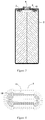
- Figure 1 shows an exemplary electrode plate in the existing technologies.
- a current collector 11 of a multilayer structure is selected for some electrode plates 1.
- the current collector 11 includes an insulating layer 111, a first conductive layer 112 and a second conductive layer 113, where the first layer 112 and the second conductive layer 113 are respectively provided to two surfaces of the insulating layer 111.
- the first conductive layer 112 includes a first body section 1121 covered by an active material layer 12 and a first protruding section 1122 protruding to an outside of the active material layer 12.
- the second conductive layer 113 includes a second body section 1131 covered by the active material layer 12 and a second protruding section 1132 protruding to an outside of the active material layer 12.
- the first protruding section 1122, the second protruding section 1132, and a section of the insulating layer 111 between the first protruding section 1122 and the second protruding section 1132 form an electric guiding section P. Since the first conductive layer 112 and the second conductive layer 113 are separated by the insulating layer 111, current cannot be transmitted between the first conductive layer 112 and the second conductive layer 113, resulting in poor current passing capacity of the electric guiding section P.
- a first conductive member 131 is usually soldered onto the first conductive layer 112
- a second conductive member 132 is usually soldered onto the second conductive layer 113
- the first conductive member 131 and the second conductive member 132 are both soldered to an adapter sheet 6 fixed to an electrode terminal.
- currents in the first conductive layer 112 and second conductive layer 113 are collected to the electrode terminal.
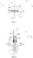
- both the first conductive member 131 and the second conductive member 132 need to be laminated together and soldered to the adapter sheet 6. This, however, will cause the first conductive member 131 and the second conductive member 132 to take a large amount of space, resulting in a reduced energy density for the secondary battery.
- the secondary battery includes an electrode assembly, a case 2, a top cap 3, an electrode terminal 4 and an adapter sheet 6.
- the electrode assembly includes a positive electrode plate 1A, a negative electrode plate 1B and a separator 5 arranged between the positive electrode plate 1A and the negative electrode plate 1B.
- the positive electrode plate 1A, the separator 5, and the negative electrode plate 1B are sequentially laminated and wound to form a jelly roll-shaped electrode assembly.
- the positive electrode plate 1A, the separator 5, and the negative electrode plate 1B may also be sequentially laminated to form a laminated electrode assembly.
- the case 2 may be of a hexahedron shape or another shape.
- An accommodating cavity is formed inside the case 2 to accommodate the electrode assembly and electrolyte.
- An opening is formed at one end of the case 2, through which the electrode assembly may be placed in the accommodating cavity of the case 2.
- the case 2 may be made of either such conductive metals as aluminum or aluminum alloy or such insulating materials as plastic.
- the top cap 3 is arranged at the case 2, covering the opening of the case 2, so that the electrode assembly is sealed inside the case 2.
- the electrode terminal 4 is arranged at the top cap 3, and an upper end of the electrode terminal 4 protrudes upwards from the top cap 3, while a lower end of the electrode terminal 4 may pass through the top cap 3 and extend into the case 2.
- the adapter sheet 6 is arranged inside the case 2, fixed to the electrode terminal 4. There are two electrode terminals 4 and two adapter sheets 6, and the positive electrode plate 1A connects to one electrode terminal 4 via one adapter sheet 6, while the negative electrode plate 1B connects to the other electrode terminal 4 via the other adapter 6.
- At least one of the positive electrode plate 1A and the negative electrode plate 1B uses an electrode plate 1 described below.
- the electrode plate 1 includes a current collector 11, an active material layer 12 and a conductive structure 13.
- the current collector 11 includes an insulating layer 111, a first conductive layer 112 and a second conductive layer 113.
- the first conductive 112 and the second conductive layer 113 are respectively arranged on two surfaces of the insulating layer 111.
- the first conductive layer 112 has a first body section 1121 and a first protruding section 1122 connected to the first body portion 1121.
- the surface of the first body section 1121 away from the insulating layer 111 is covered by the active material layer 12, while the surface of the first protruding section 1122 away from the insulating layer 111 is not covered by the active material layer 12.
- the second conductive layer 113 has a second body section 1131 and a second protruding section 1132 connected to the second body section 1131.
- the surface of the second body section 1131 away from the insulating layer 111 is covered by the active material layer 12, while the surface of the second protruding section 1132 away from the insulating layer 111 is not covered by the active material layer 12.
- a conductive structure 13 includes a first conductive member 131 connected to the first protruding section 1122 and a second conductive member 132 connected to the second protruding section 1132.
- the second conductive member 132 is bent towards and connected to the first conductive member 131.
- the second conductive member 132 may either directly connect the first conductive member 131, or indirectly connect the first conductive member 131 via the first protruding section 1122.
- the first conductive member 131 extends away from the active material layer 12 beyond the second conductive member 132.
- a part of the first conductive member 131 extends beyond the second conductive member 132 in the direction away from the active material layer 12, the part of the first conductive member 131 beyond the second conductive member 132 is defined as a current collecting section C.
- the first protruding section 1122, the second protruding section 1132, and a section of the insulating layer 111 between the first protruding section 1122 and the second protruding section 1132 form an electric guiding section P.
- the electrode assembly has a plurality of electric guiding sections P and a plurality of conductive structures 13, the plurality of electric guiding sections P are arranged to be laminated.
- the current collecting section C of one conductive structure 13 contacts with the current collecting section C of another conductive structure 13.
- each current collecting section C of the plurality of conductive structures 13 are connected to the adapter sheet 6, and each second conductive member 132 of the plurality of conductive structures 13 is located at a side of the current collecting section C away from the adapter sheet 6.
- the current collecting section C of the plurality of conductive structures 13 may be soldered to the adapter sheet 6 in the first place. Then with reference to Figures 3 and 9 , the second conductive member 132 is flipped to the lower side of the adapter sheet 6 via the bent current collecting section C.
- the first and/or conductive layer has a thickness of 0.1 ⁇ 10um, for example, 0.1um, 1um, 2 um, 3 um, 4 um, 5 um, 6 um, 7 um, 8 um, 9 um, 10 um. In some embodiments, the first and/or conductive layer has a thickness of 0.7-0.9 um, for example, 0.7 um, 0.8 um, 0.9 um.
- the first conductive member 131 and the second conductive member 132 may collect current in the first conductive layer 112 and the second conductive layer 113 to the adapter sheet 6, thereby improving current passing capacity.
- the currents in the first conductive layer 112 and the second conductive layer 113 may be collected to the adapter sheet 6 by simply connecting the current collecting section C of the first conductive member 131 to the adapter sheet 6 without the need for the second conductive member 132 to be connected to the adapter sheet 6. Therefore, the present application may reduce the overall thickness after the adapter sheet 6 and the conductive structure 13 are connected together and the space taken by the conductive structure 13, and improves energy density of the secondary battery, as compared with existing technologies.
- the second conductive member 132 includes a first connecting section 1321 connected to the second protruding section 1132, second connecting section 1323 connected to the first conductive member 131, and a bent section 1322 bent towards the first conductive member 131 relatively to the first connecting section 1321.
- the bent section 1322 is connected between the first connecting section 1321 and the second connecting section 1323.
- the electrode plate 1 can be formed differently, as explained below.
- first metal foils are soldered to the first conductive layer 112 and the second conductive layer 113. Then the two metal foils are bent and connected. Finally, the first protruding section 1122, the second protruding section 1132, the first conductive member 131 and the second conductive member 132 of desired shapes are formed by cutting the first conductive layer 112, the second conductive layer 113 and the two metal foils. At this time, the bent portion 1322 is preferably located on the side of the second protruding section 1132 away from the active material layer 12, so that the bending of the second conductive member 132 may be completed before the cutting process.
- the forming method may simultaneously form at least two first conductive members 131 and second conductive members 132 to facilitate continuous production.
- first conductive layer 112 and the second conductive layer 113 are firstly cut to form a first protruding section 1122 and a second protruding section 1132 of desired shapes. Then the cut first conductive member 131 and the cut second conductive member 132 are respectively soldered to the first protruding section 1122 and the second protruding section 1132. Finally, the second conductive member 132 is folded and connected to the first conductive member 131.
- the bent section 1322 may be located on the side of the electric guiding section P in the length direction X. At this time, the end of the electric guiding section P away from the active material layer 12 may extend beyond the end of the second conductive member 132 away from the active material layer 12.
- the second conductive member 132 does not take additional space in the height direction Z.
- electrode plate 1 of the present disclosure will now be described below.
- Figure 8 shows a first exemplary electrode plate according to some embodiments of the present disclosure.
- the second connecting section 1323 is bent towards the active material layer 12 relatively to the bent section 1322, and the second connecting section 1323 is connected between the first conductive member 131 and the first protruding section 1122.
- the second connecting section 1323 is located on the side of the bent section 1322 closer to the active material layer 12, and the section of the first conductive member 131 beyond the bent section 1322 is the current collecting section C. Accordingly, the length of the current collecting section C may be increased relatively.
- the first conductive member 131, the second connecting section 1323, and the first protruding section 1122 may be integrally soldered together, therefore a first fusion region W1 is formed.
- Insulating cement may be disposed on the surface of the first fusion region W1 and the surface of the first fusion region W1 is away from the insulating layer 111.
- the first connecting section 1321 may also be fixed to the second protruding section 1132 by soldering. It can be understood by the skilled person that in one example after the soldering, particles of the soldering materials may be formed onto the surface of the first fusion region W1 which is away from the insulating layer 111. Due to the insulating cement, the particles can be fixed in the insulating cement, and thus the particles are prevented from moving onto other parts of the electrode plate. Therefore, undesired short circuit caused by the particles can be effectively avoided.
- Figure 10 shows a second exemplary electrode plate according to some embodiments of the present disclosure.
- the second connecting section 1323 is bent towards the active material layer 12 relatively to the bent section 1322, and the second connecting section 1323 is connected between the first conductive member 131 and the first protruding section 1122.
- the conductive structure 13 is an integrally formed piece, and an end of the first conductive member 131 closer to the active material layer 12 is connected to an end of the second connecting section 1323 that is closer to the active material layer 12.
- the strength of the conductive structure 13 can be improved and it is easier to manufacture and assemble the electrode plate.
- the conductive structure 13 may be assembled according to the following steps. First, the conductive structure 13 is soldered to the second protruding section 1132. Then the section of the conductive structure 13 beyond the electric guiding section P is bent onto the first protruding section 1122, and the conductive structure 13 is soldered to the first protruding section 1122. Finally, the conductive structure 13 is bent again to form the first conductive member 131.
- Figure 11 shows a third exemplary electrode plate according to some embodiments of the present disclosure.
- the second connecting section 1323 is bent towards the active material layer 12 relatively to the bent section 1322, and the second connecting portion 1323 is connected between the first conductive member 131 and the first protruding section 1122.
- the conductive structure 13 is integrally formed, and an end of the first conductive member 131 closer to the active material layer 12 is connected to an end of the second connecting portion 1323 closer to the active material layer 12.
- the first conductive member 131, the second connecting portion 1323, and the first protruding section 1122 are integrally soldered together, and the first fusion region W1 can be formed.
- the third exemplary electrode plate can increase the current passing area between the first conductive member 131 and the second connecting section 1323.
- Figure 12 shows a fourth exemplary electrode plate according to some embodiments of the present disclosure.
- the second connecting section 1323 is bent towards the active material layer 12 relatively to the bent section 1322, and the second connecting portion 1323 is connected between the first conductive member 131 and the first protruding section 1122.
- the first conductive member 131 is connected to a section of the first protruding section 1122 between the second connecting section 1323 and the active material layer 12, and the first conductive member 131 is indirectly connected to the second connecting section 1323 via the first protruding section 1122.
- the first conductive member 131 is soldered to the first protruding section 1122 and forms a second fusion region W2, and the second connecting section 1323 is located on a side of the second fusion region W2 away from the active material layer 12.
- an effect of the exemplary electrode plate is to further increase the current passing area between the first conductive member 131 and the second connecting section 1323. This is due to the presence of the second fusion region W2 and the close contact between first conductive member 131 and the second connecting section 1323.
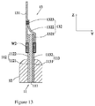
- Figure 13 shows a fifth exemplary electrode plate according to some embodiments of the present disclosure.
- the second connecting section 1323 is connected to an end of the bent section 1322 that is closer to the first conductive member 131, and extends away from the current collector 11.
- the first conductive member 131 and the second conductive member 132 are firstly soldered to the first protruding region 1122 and the second protruding region 1132, respectively.
- the section of the second conductive member 132 beyond the electric guiding section P is bent onto the first conductive member 131.
- the first conductive member 131 and the second conductive member 132 are soldered together.
- the manufacturing process of bending the second conductive member 132 is simple.
- the current in the first conductive layer and the second conductive layer may be collected to the adapter sheet simply by connecting the current collector of the first conductive member to the adapter sheet without connecting the second conductive member to the adapter sheet. Therefore, compared with the existing technologies, the present application may reduce an overall thickness after the adapter sheet and conductive structure are connected together, so that the space taken by a conductive structure is reduced and the energy density of the secondary battery is improved.
Landscapes
- Chemical & Material Sciences (AREA)
- Chemical Kinetics & Catalysis (AREA)
- Electrochemistry (AREA)
- General Chemical & Material Sciences (AREA)
- Engineering & Computer Science (AREA)
- Manufacturing & Machinery (AREA)
- Materials Engineering (AREA)
- Composite Materials (AREA)
- Life Sciences & Earth Sciences (AREA)
- Biophysics (AREA)
- Computer Hardware Design (AREA)
- Connection Of Batteries Or Terminals (AREA)
- Secondary Cells (AREA)
Abstract
Description
- The present disclosure relates to battery technologies, and more particularly to a secondary battery and an electrode plate.
- A typical secondary battery includes an electrode plate, and the electrode plate generally includes a current collector and an active material layer coated on a surface of the current collector. Further, the current collector includes a sandwich structure that has a conductive layer, an insulating layer and a conductive layer. To allow a current channel between the sandwich structure and an electrode terminal of the secondary battery, two additional metal sheets are arranged to connect to the sandwich structure.
- Some embodiments of the present disclosure provide a secondary battery and an electrode plate, which can reduce the space of a conductive structure and improve energy density of the secondary battery.
- The electrode plate includes a current collector, an active material layer and a conductive structure. The current collector includes an insulating layer, a first conductive layer and a second conductive layer, and the first conductive layer and the second conductive layer are respectively arranged on two surfaces of the insulating layer. The first conductive layer has a first body section and a first protruding section arranged to connect to the first body section, and a surface of the first body section that is away from the insulating layer is covered by the active material layer, while a surface of the first protruding section that is away from the insulating layer is not covered by the active material layer. The second conductive layer has a second body section and a second protruding section arranged to connect to the second body section, and a surface of the second body section which is away from the insulating layer is covered by the active material layer, while a surface of the second protruding section that is away from the insulating layer is not covered by the active material layer.
- The conductive structure includes a first conductive member arranged to connect to the first protruding section and a second conductive member arranged to connect to the second protruding section. The second conductive member is bent towards the first conductive member and connects to the first conductive member, and wherein the first conductive member extends away from the active material layer and is beyond the second conductive member.
- In some embodiments, the second conductive member includes a first connecting section arranged to connect to the second protruding section, a bent section bent towards the first conductive member relatively to the first connecting section, and a second connecting section arranged to connect to the first conductive member. The bent section connects the first connecting section with the second connecting section.
- In some embodiments, the bent section is located at a side of the second protruding section away from the active material layer.
- In some embodiments, the second connecting section connects the first conductive member with the first protruding section, the second connecting section is bent towards the active material layer relatively to the bent portion.
- In some embodiments, the conductive structure is integrally formed, and an end of the first conductive member that is closer to the active material layer connects to an end of the second connecting section, the end of the second connecting section is closer to the active material layer.
- In some embodiments, a fusion region is formed to connect the first conductive member, the second connecting section and the first protruding section.
- In some embodiments, the first conductive member connects to a section of the first protruding section, the section being located between the second connecting section and the active material layer.
- In some embodiments, the second connecting section connects to an end of the bent section that is closer to the first conductive member and extends away from the current collector.
- In some embodiments, the first conductive layer has a thickness of 0.7-0.9 um.
- In some embodiments, the second conductive layer has a thickness of 0.7-0.9 um.
- The secondary battery has an electrode assembly including the electrode plate described above.
- In some embodiments, the first protruding section, the second protruding section and a section of the insulating layer located between the first protruding section and the second protruding section form an electric guiding section. The electrode assembly has at least two electric guiding sections and at least two conductive structures, and the at least two electrical guiding sections are laminated. The section of the first conductive member beyond the second conductive member is a current collecting section, and a current collecting section of one conductive structure contacts a current collecting section of an adjacent conductive structure.
- In some embodiments, the secondary battery includes an electrode terminal and an adapter sheet arranged to connect to the electrode terminal, each current collecting section of the at least two conductive structures connects to the adapter sheet, and each second conductive member of the at least two conductive structures are located on a side of the current collecting section that is away from the adapter sheet.
- Advantageous effects of some embodiments of the present disclosure lie in the following. In the secondary battery of some embodiments of the present application, the current in the first conductive layer and the second conductive layer may be collected to the adapter sheet simply by connecting the current collector of the first conductive member to the adapter sheet without connecting the second conductive member to the adapter sheet. Therefore, compared with the existing technologies, the embodiments of the present application may reduce an overall thickness after the adapter sheet and conductive structure are connected together, so that the space taken by a conductive structure is reduced and the energy density of the secondary battery is improved.
-
-
Figure 1 is a schematic view of an exemplary electrode plate in the existing technologies. -
Figure 2 is a schematic view showing a connection between an exemplary electrode plate and an exemplary adapter sheet in the existing technologies. -
Figure 3 is a schematic view of an exemplary secondary battery according to some embodiment of the present disclosure. -
Figure 4 is a schematic view of an electrode assembly for an exemplary secondary battery according to some embodiments of the present disclosure. -
Figure 5 is a schematic view of an exemplary electrode plate according to some embodiments of the present disclosure. -
Figure 6 is another schematic view of an electrode plate of an embodiment of the present disclosure. -
Figure 7 is an enlarged view of the dotted line part ofFigure 6 . -
Figure 8 is a sectional view along the A-A line. -
Figure 9 is a schematic view showing a connection between the exemplary electrode plate and the exemplary adapter sheet inFigure 8 . -
Figures 10 to 13 are schematic views of exemplary electrode plates according to some embodiments of the present disclosure. - The following detailed description is merely exemplary in nature and is not intended to limit the application and uses. Furthermore, there is no intention to be bound by any theory presented in the preceding background or summary or the following detailed description.
- In the description of the present disclosure, it should be understood that the singular forms, "a," "an," and "the" are intended to include the plural forms as well, unless context clearly indicates otherwise.
-
Figure 1 shows an exemplary electrode plate in the existing technologies. In order to improve safety performance of the secondary battery, acurrent collector 11 of a multilayer structure is selected for someelectrode plates 1. With reference toFigure 1 , thecurrent collector 11 includes aninsulating layer 111, a firstconductive layer 112 and a secondconductive layer 113, where thefirst layer 112 and the secondconductive layer 113 are respectively provided to two surfaces of theinsulating layer 111. The firstconductive layer 112 includes afirst body section 1121 covered by anactive material layer 12 and afirst protruding section 1122 protruding to an outside of theactive material layer 12. The secondconductive layer 113 includes asecond body section 1131 covered by theactive material layer 12 and asecond protruding section 1132 protruding to an outside of theactive material layer 12. Thefirst protruding section 1122, thesecond protruding section 1132, and a section of theinsulating layer 111 between thefirst protruding section 1122 and thesecond protruding section 1132 form an electric guiding section P. Since the firstconductive layer 112 and the secondconductive layer 113 are separated by theinsulating layer 111, current cannot be transmitted between the firstconductive layer 112 and the secondconductive layer 113, resulting in poor current passing capacity of the electric guiding section P. In order to improve the current passing capacity thereof, a firstconductive member 131 is usually soldered onto the firstconductive layer 112, a secondconductive member 132 is usually soldered onto the secondconductive layer 113, and the firstconductive member 131 and the secondconductive member 132 are both soldered to anadapter sheet 6 fixed to an electrode terminal. Thereby, currents in the firstconductive layer 112 and secondconductive layer 113 are collected to the electrode terminal. In the secondary battery, in order to improve the current passing capacity, there are generally a plurality of the electric guiding sections P that are laminated, on each of which the firstconductive member 131 and the secondconductive member 132 are required to be soldered. With reference toFigure 2 , both the firstconductive member 131 and the secondconductive member 132 need to be laminated together and soldered to theadapter sheet 6. This, however, will cause the firstconductive member 131 and the secondconductive member 132 to take a large amount of space, resulting in a reduced energy density for the secondary battery. - A secondary battery and an electrode thereof according to some embodiments of the present disclosure will be described in details below with reference to the drawings.
- With reference to
Figure 3 , the secondary battery includes an electrode assembly, acase 2, atop cap 3, an electrode terminal 4 and anadapter sheet 6. - With reference to
Figure 4 , the electrode assembly includes apositive electrode plate 1A, anegative electrode plate 1B and aseparator 5 arranged between thepositive electrode plate 1A and thenegative electrode plate 1B. In one embodiment, thepositive electrode plate 1A, theseparator 5, and thenegative electrode plate 1B are sequentially laminated and wound to form a jelly roll-shaped electrode assembly. In another embodiment, thepositive electrode plate 1A, theseparator 5, and thenegative electrode plate 1B may also be sequentially laminated to form a laminated electrode assembly. - The
case 2 may be of a hexahedron shape or another shape. An accommodating cavity is formed inside thecase 2 to accommodate the electrode assembly and electrolyte. An opening is formed at one end of thecase 2, through which the electrode assembly may be placed in the accommodating cavity of thecase 2. Thecase 2 may be made of either such conductive metals as aluminum or aluminum alloy or such insulating materials as plastic. - The
top cap 3 is arranged at thecase 2, covering the opening of thecase 2, so that the electrode assembly is sealed inside thecase 2. The electrode terminal 4 is arranged at thetop cap 3, and an upper end of the electrode terminal 4 protrudes upwards from thetop cap 3, while a lower end of the electrode terminal 4 may pass through thetop cap 3 and extend into thecase 2. Theadapter sheet 6 is arranged inside thecase 2, fixed to the electrode terminal 4. There are two electrode terminals 4 and twoadapter sheets 6, and thepositive electrode plate 1A connects to one electrode terminal 4 via oneadapter sheet 6, while thenegative electrode plate 1B connects to the other electrode terminal 4 via theother adapter 6. - In the secondary battery, at least one of the
positive electrode plate 1A and thenegative electrode plate 1B uses anelectrode plate 1 described below. - With reference to
Figures 5 to 8 , theelectrode plate 1 includes acurrent collector 11, anactive material layer 12 and aconductive structure 13. Thecurrent collector 11 includes an insulatinglayer 111, a firstconductive layer 112 and a secondconductive layer 113. The first conductive 112 and the secondconductive layer 113 are respectively arranged on two surfaces of the insulatinglayer 111. The firstconductive layer 112 has afirst body section 1121 and afirst protruding section 1122 connected to thefirst body portion 1121. The surface of thefirst body section 1121 away from the insulatinglayer 111 is covered by theactive material layer 12, while the surface of the first protrudingsection 1122 away from the insulatinglayer 111 is not covered by theactive material layer 12. The secondconductive layer 113 has asecond body section 1131 and asecond protruding section 1132 connected to thesecond body section 1131. The surface of thesecond body section 1131 away from the insulatinglayer 111 is covered by theactive material layer 12, while the surface of thesecond protruding section 1132 away from the insulatinglayer 111 is not covered by theactive material layer 12. - A
conductive structure 13 includes a firstconductive member 131 connected to the first protrudingsection 1122 and a secondconductive member 132 connected to thesecond protruding section 1132. The secondconductive member 132 is bent towards and connected to the firstconductive member 131. The secondconductive member 132 may either directly connect the firstconductive member 131, or indirectly connect the firstconductive member 131 via the first protrudingsection 1122. The firstconductive member 131 extends away from theactive material layer 12 beyond the secondconductive member 132. In other words, with reference toFigure 8 , a part of the firstconductive member 131 extends beyond the secondconductive member 132 in the direction away from theactive material layer 12, the part of the firstconductive member 131 beyond the secondconductive member 132 is defined as a current collecting section C. - With reference to
Figure 9 , the first protrudingsection 1122, thesecond protruding section 1132, and a section of the insulatinglayer 111 between the first protrudingsection 1122 and thesecond protruding section 1132 form an electric guiding section P. In the secondary battery, the electrode assembly has a plurality of electric guiding sections P and a plurality ofconductive structures 13, the plurality of electric guiding sections P are arranged to be laminated. The current collecting section C of oneconductive structure 13 contacts with the current collecting section C of anotherconductive structure 13. - With reference to
Figure 9 , each current collecting section C of the plurality ofconductive structures 13 are connected to theadapter sheet 6, and each secondconductive member 132 of the plurality ofconductive structures 13 is located at a side of the current collecting section C away from theadapter sheet 6. In a forming process of the secondary battery, the current collecting section C of the plurality ofconductive structures 13 may be soldered to theadapter sheet 6 in the first place. Then with reference toFigures 3 and9 , the secondconductive member 132 is flipped to the lower side of theadapter sheet 6 via the bent current collecting section C. - In the secondary battery, since the
current collector 11 of theelectrode plate 1 is provided with the insulatinglayer 111, the thicknesses of the firstconductive layer 112 and secondconductive layer 113 can be reduced. In some embodiments, the first and/or conductive layer has a thickness of 0.1∼10um, for example, 0.1um, 1um, 2 um, 3 um, 4 um, 5 um, 6 um, 7 um, 8 um, 9 um, 10 um. In some embodiments, the first and/or conductive layer has a thickness of 0.7-0.9 um, for example, 0.7 um, 0.8 um, 0.9 um. When an external object pierces theelectrode plate 1, due to small thicknesses of the firstconductive layer 112 and secondconductive layer 113, the firstconductive layer 112 and the secondconductive layer 113 have small burrs generated at the portion pierced by the external object. It is therefore difficult to pierce theseparator 5, and consequently short circuit is avoided and safety performance is improved. The firstconductive member 131 and the secondconductive member 132 may collect current in the firstconductive layer 112 and the secondconductive layer 113 to theadapter sheet 6, thereby improving current passing capacity. - With reference to
Figure 9 , in the secondary battery of the present application, the currents in the firstconductive layer 112 and the secondconductive layer 113 may be collected to theadapter sheet 6 by simply connecting the current collecting section C of the firstconductive member 131 to theadapter sheet 6 without the need for the secondconductive member 132 to be connected to theadapter sheet 6. Therefore, the present application may reduce the overall thickness after theadapter sheet 6 and theconductive structure 13 are connected together and the space taken by theconductive structure 13, and improves energy density of the secondary battery, as compared with existing technologies. - With reference to
Figure 8 , the secondconductive member 132 includes a first connectingsection 1321 connected to thesecond protruding section 1132, second connectingsection 1323 connected to the firstconductive member 131, and abent section 1322 bent towards the firstconductive member 131 relatively to the first connectingsection 1321. Thebent section 1322 is connected between the first connectingsection 1321 and the second connectingsection 1323. By bending the secondconductive member 132, the secondconductive member 132 may be connected to the firstconductive member 131, and the space taken by the secondconductive member 132 in the height direction Z may also be reduced, so as to ensure that the current collecting section C is reserved for the firstconductive member 131. - As two examples, the
electrode plate 1 can be formed differently, as explained below. - In one example, two metal foils are soldered to the first
conductive layer 112 and the secondconductive layer 113. Then the two metal foils are bent and connected. Finally, the first protrudingsection 1122, thesecond protruding section 1132, the firstconductive member 131 and the secondconductive member 132 of desired shapes are formed by cutting the firstconductive layer 112, the secondconductive layer 113 and the two metal foils. At this time, thebent portion 1322 is preferably located on the side of thesecond protruding section 1132 away from theactive material layer 12, so that the bending of the secondconductive member 132 may be completed before the cutting process. The forming method may simultaneously form at least two firstconductive members 131 and secondconductive members 132 to facilitate continuous production. - In another example, the first
conductive layer 112 and the secondconductive layer 113 are firstly cut to form afirst protruding section 1122 and asecond protruding section 1132 of desired shapes. Then the cut firstconductive member 131 and the cut secondconductive member 132 are respectively soldered to the first protrudingsection 1122 and thesecond protruding section 1132. Finally, the secondconductive member 132 is folded and connected to the firstconductive member 131. When this forming method is adopted, thebent section 1322 may be located on the side of the electric guiding section P in the length direction X. At this time, the end of the electric guiding section P away from theactive material layer 12 may extend beyond the end of the secondconductive member 132 away from theactive material layer 12. The secondconductive member 132 does not take additional space in the height direction Z. - Some examples the
electrode plate 1 of the present disclosure will now be described below. -
Figure 8 shows a first exemplary electrode plate according to some embodiments of the present disclosure. With reference toFigure 8 , the second connectingsection 1323 is bent towards theactive material layer 12 relatively to thebent section 1322, and the second connectingsection 1323 is connected between the firstconductive member 131 and the first protrudingsection 1122. At this time, the second connectingsection 1323 is located on the side of thebent section 1322 closer to theactive material layer 12, and the section of the firstconductive member 131 beyond thebent section 1322 is the current collecting section C. Accordingly, the length of the current collecting section C may be increased relatively. - The first
conductive member 131, the second connectingsection 1323, and the first protrudingsection 1122 may be integrally soldered together, therefore a first fusion region W1 is formed. Insulating cement may be disposed on the surface of the first fusion region W1 and the surface of the first fusion region W1 is away from the insulatinglayer 111. The first connectingsection 1321 may also be fixed to thesecond protruding section 1132 by soldering. It can be understood by the skilled person that in one example after the soldering, particles of the soldering materials may be formed onto the surface of the first fusion region W1 which is away from the insulatinglayer 111. Due to the insulating cement, the particles can be fixed in the insulating cement, and thus the particles are prevented from moving onto other parts of the electrode plate. Therefore, undesired short circuit caused by the particles can be effectively avoided. -
Figure 10 shows a second exemplary electrode plate according to some embodiments of the present disclosure. With reference toFigure 10 , the second connectingsection 1323 is bent towards theactive material layer 12 relatively to thebent section 1322, and the second connectingsection 1323 is connected between the firstconductive member 131 and the first protrudingsection 1122. Theconductive structure 13 is an integrally formed piece, and an end of the firstconductive member 131 closer to theactive material layer 12 is connected to an end of the second connectingsection 1323 that is closer to theactive material layer 12. In this example, due to the integral form the strength of theconductive structure 13 can be improved and it is easier to manufacture and assemble the electrode plate. - The
conductive structure 13 may be assembled according to the following steps. First, theconductive structure 13 is soldered to thesecond protruding section 1132. Then the section of theconductive structure 13 beyond the electric guiding section P is bent onto the first protrudingsection 1122, and theconductive structure 13 is soldered to the first protrudingsection 1122. Finally, theconductive structure 13 is bent again to form the firstconductive member 131. -
Figure 11 shows a third exemplary electrode plate according to some embodiments of the present disclosure. With reference toFigure 11 , the second connectingsection 1323 is bent towards theactive material layer 12 relatively to thebent section 1322, and the second connectingportion 1323 is connected between the firstconductive member 131 and the first protrudingsection 1122. Theconductive structure 13 is integrally formed, and an end of the firstconductive member 131 closer to theactive material layer 12 is connected to an end of the second connectingportion 1323 closer to theactive material layer 12. The firstconductive member 131, the second connectingportion 1323, and the first protrudingsection 1122 are integrally soldered together, and the first fusion region W1 can be formed. Compared with the second exemplary electrode plate, the third exemplary electrode plate can increase the current passing area between the firstconductive member 131 and the second connectingsection 1323. -
Figure 12 shows a fourth exemplary electrode plate according to some embodiments of the present disclosure. With reference toFigure 12 , the second connectingsection 1323 is bent towards theactive material layer 12 relatively to thebent section 1322, and the second connectingportion 1323 is connected between the firstconductive member 131 and the first protrudingsection 1122. The firstconductive member 131 is connected to a section of the first protrudingsection 1122 between the second connectingsection 1323 and theactive material layer 12, and the firstconductive member 131 is indirectly connected to the second connectingsection 1323 via the first protrudingsection 1122. The firstconductive member 131 is soldered to the first protrudingsection 1122 and forms a second fusion region W2, and the second connectingsection 1323 is located on a side of the second fusion region W2 away from theactive material layer 12. In one example, an effect of the exemplary electrode plate is to further increase the current passing area between the firstconductive member 131 and the second connectingsection 1323. This is due to the presence of the second fusion region W2 and the close contact between firstconductive member 131 and the second connectingsection 1323. -
Figure 13 shows a fifth exemplary electrode plate according to some embodiments of the present disclosure. With reference toFigure 13 , the second connectingsection 1323 is connected to an end of thebent section 1322 that is closer to the firstconductive member 131, and extends away from thecurrent collector 11. During assembling, the firstconductive member 131 and the secondconductive member 132 are firstly soldered to the firstprotruding region 1122 and the secondprotruding region 1132, respectively. Then, the section of the secondconductive member 132 beyond the electric guiding section P is bent onto the firstconductive member 131. Finally, the firstconductive member 131 and the secondconductive member 132 are soldered together. In this example, the manufacturing process of bending the secondconductive member 132 is simple. - Advantageous effects of the present disclosure lie in the following. In the secondary battery of the present application, the current in the first conductive layer and the second conductive layer may be collected to the adapter sheet simply by connecting the current collector of the first conductive member to the adapter sheet without connecting the second conductive member to the adapter sheet. Therefore, compared with the existing technologies, the present application may reduce an overall thickness after the adapter sheet and conductive structure are connected together, so that the space taken by a conductive structure is reduced and the energy density of the secondary battery is improved.
- While specific embodiments of the invention have been described above, it will be appreciated that the invention may be practiced otherwise than as described. The descriptions above are intended to be illustrative, not limiting. Thus, it will be apparent to one skilled in the art that modifications may be made to the invention as described without departing from the scope of the claims set out below.
- It is to be appreciated that the Detailed Description section, and not the Summary and Abstract sections, is intended to be used to interpret the claims. The Summary and Abstract sections may set forth one or more but not all exemplary embodiments of the present invention as contemplated by the inventor(s), and thus, are not intended to limit the present invention and the appended claims in any way.
- The foregoing description of the specific embodiments will so fully reveal the general nature of the invention that others can, by applying knowledge within the skill of the art, readily modify and/or adapt for various applications such specific embodiments, without undue experimentation, without departing from the general concept of the present invention. Therefore, such adaptations and modifications are intended to be within the meaning and range of equivalents of the disclosed embodiments, based on the teaching and guidance presented herein. It is to be understood that the phraseology or terminology herein is for the purpose of description and not of limitation, such that the terminology or phraseology of the present specification is to be interpreted by the skilled artisan in light of the teachings and guidance.
- The breadth and scope of the present invention should not be limited by any of the above-described exemplary embodiments, but should be defined only in accordance with the following claims and their equivalents.
| 1 | |
1323 | second connecting |
|
| 11 | |
1A | |
|
| 111 | |
1B | |
|
| 112 | first |
2 | |
|
| 1121 | |
3 | |
|
| 1122 | first protruding section | 4 | |
|
| 113 | second |
5 | |
|
| 1131 | |
6 | |
|
| 1132 | second protruding section | C | current collecting |
|
| 12 | active material layer | P | electric guiding |
|
| 13 | conductive structure | W1 | |
|
| 131 | first conductive member | W2 | |
|
| 132 | second conductive member | | length direction | |
| 1321 | first connecting section | | thickness direction | |
| 1322 | bent section | Z | height direction |
Claims (12)
- An electrode plate (1) for a secondary battery, comprising:an active material layer (12);a current collector (11), comprising:an insulating layer (111);a first conductive layer (112), comprising;a first body section (1121), wherein a surface of the first body section (1121) that is away from the insulating layer (111) is covered by the active material layer (12);a first protruding section (1122) arranged to connect to the first body section (1121), wherein a surface of the first protruding section (1122) that is away from the insulating layer (111) is not covered by the active material layer (12);a second conductive layer (113), comprising:a second body section (1131), wherein a surface of the second body section (1131) that is away from the insulating layer (111) is covered by the active material layer (12);a second protruding section (1132) arranged to connect to the second body section (1131), wherein a surface of the second protruding section (1132) that is away from the insulating layer (111) is not covered by the active material layer (12);wherein the first conductive layer (112) and the second conductive layer (113) are respectively arranged on two surfaces of the insulating layer (111);a conductive structure (13), comprising:a first conductive member (131) arranged to connect to the first protruding section (1122);a second conductive member (132) arranged to connect to the second protruding section (1132);wherein, the second conductive member (132) is bent towards the first conductive member (131) and connects to the first conductive member (131), and wherein the first conductive member (131) extends away from the active material layer (12) and is beyond the second conductive member (132).
- The electrode plate (1) according to claim 1, wherein, the second conductive member (132) comprises:a first connecting section (1321) arranged to connect to the second protruding section (1132);a bent section (1322), bent towards the first conductive member (131) relatively to the first connecting section (1321); anda second connecting section (1323) arranged to connect to the first conductive member (131);wherein, the bent section (1322) connects the first connecting section (1321) with the second connecting section (1323).
- The electrode plate (1) according to claim 2, wherein the bent section (1322) is located at a side of the second protruding section (1132), the side being away from the active material layer (12).
- The electrode plate (1) according to claim 2 or 3, wherein the second connecting section (1323) is bent towards the active material layer (12) relatively to the bent portion (1322) and connects the first conductive member (131) with the first protruding section (1122).
- The electrode plate (1) according to any one of claims 2 to 4, wherein the conductive structure (13) is integrally formed, and an end of the first conductive member (131) that is closer to the active material layer (12) connects to an end of the second connecting section (1323) that is closer to the active material layer (12).
- The electrode plate (1) according to any one of claims 2 to 4, wherein the first conductive member (131) connects to a section of the first protruding section (1122), the section being located between the second connecting section (1323) and the active material layer (12).
- The electrode plate (1) according to claim 2 or 3, wherein the second connecting section (1323) connects to an end of the bent section (1322), the end of the bent section (1322) is closer to the first conductive member (131) and extends away from the current collector (11).
- The electrode plate (1) according to any one of the preceding claims, wherein the first conductive layer (112) has a thickness of 0.7-0.9 um.
- The electrode plate (1) according to any one of the preceding claims, wherein the second conductive layer (113) has a thickness of 0.7-0.9 um.
- A secondary battery, comprising an electrode assembly that comprises the electrode plate (1) according to any one of claims 1 to 9.
- The secondary battery according to claim 10, wherein the first protruding section (1122), the second protruding section (1132) and a section of the insulating layer (111) located between the first protruding section (1122) and the second protruding section (1132) form an electric guiding section (P);
wherein the electrode assembly has at least two electric guiding sections (P) and at least two conductive structures (13), and the at least two electrical guiding sections (P) are laminated;
wherein the section of the first conductive member (131) beyond the second conductive member (132) is a current collecting section (C), and a current collecting section (C) of one of the at least two conductive structure (13) contacts a current collecting section (C) of an adjacent conductive structure (13). - The secondary battery according to claim 11, wherein the secondary battery further includes an electrode terminal (4) and an adapter sheet (6) that is arranged to connect to the electrode terminal (4), each current collecting section (C) of the at least two conductive structures (13) is connected to the adapter sheet (6), and each second conductive member (132) of the at least two conductive structures (13) is located on a side of the current collecting section (C) away from the adapter sheet (6).
Priority Applications (1)
| Application Number | Priority Date | Filing Date | Title |
|---|---|---|---|
| PL18248114T PL3595044T3 (en) | 2018-07-13 | 2018-12-28 | BATTERY AND ELECTRODE PLATE |
Applications Claiming Priority (1)
| Application Number | Priority Date | Filing Date | Title |
|---|---|---|---|
| CN201810768859.5A CN108963311B (en) | 2018-07-13 | 2018-07-13 | Secondary battery and pole piece thereof |
Publications (2)
| Publication Number | Publication Date |
|---|---|
| EP3595044A1 true EP3595044A1 (en) | 2020-01-15 |
| EP3595044B1 EP3595044B1 (en) | 2021-07-28 |
Family
ID=64483194
Family Applications (1)
| Application Number | Title | Priority Date | Filing Date |
|---|---|---|---|
| EP18248114.3A Active EP3595044B1 (en) | 2018-07-13 | 2018-12-28 | Secondary battery and electrode plate |
Country Status (5)
| Country | Link |
|---|---|
| US (3) | US20200020952A1 (en) |
| EP (1) | EP3595044B1 (en) |
| CN (2) | CN111244388B (en) |
| HU (1) | HUE056627T2 (en) |
| PL (1) | PL3595044T3 (en) |
Cited By (2)
| Publication number | Priority date | Publication date | Assignee | Title |
|---|---|---|---|---|
| EP4576241A4 (en) * | 2022-11-14 | 2025-12-31 | Contemporary Amperex Technology Hong Kong Ltd | Electrode component, battery cell, battery and electrical device |
| EP4618301A4 (en) * | 2023-11-01 | 2026-04-22 | Lg Energy Solution Ltd | ELECTRODE ARRANGEMENT FOR SECONDARY BATTERY AND BATTERY CELL SO THAT |
Families Citing this family (18)
| Publication number | Priority date | Publication date | Assignee | Title |
|---|---|---|---|---|
| KR102112227B1 (en) * | 2018-07-27 | 2020-05-18 | 주식회사 유앤에스에너지 | Current collector for electrodes |
| CN210805919U (en) | 2019-10-16 | 2020-06-19 | 宁德时代新能源科技股份有限公司 | Secondary battery and electrode member thereof, battery module, and device using secondary battery |
| US20220416372A1 (en) * | 2019-11-19 | 2022-12-29 | Xiamen Hithium New Energy Technology Co., Ltd. | Electrode plate of secondary battery and preparation method thereof, secondary battery |
| CN112825381A (en) * | 2019-11-19 | 2021-05-21 | 深圳市海鸿新能源技术有限公司 | Pole piece of secondary battery, preparation method of pole piece and secondary battery |
| CA3163083A1 (en) * | 2019-11-27 | 2021-06-03 | Soteria Battery Innovation Group Inc. | Battery connections and metalized film components in energy storage devices having internal fuses |
| CN111509180B (en) * | 2020-03-26 | 2022-04-12 | 合肥国轩高科动力能源有限公司 | Lithium battery cell with conductive tabs |
| CN114583178A (en) * | 2020-11-30 | 2022-06-03 | 比亚迪股份有限公司 | A battery current collector and lithium ion battery |
| CN115117462B (en) * | 2021-03-18 | 2025-04-22 | 宁德新能源科技有限公司 | Cells, battery packs and electronic devices |
| WO2022205011A1 (en) * | 2021-03-30 | 2022-10-06 | 宁德新能源科技有限公司 | Battery and electronic device applying same |
| HUE070435T2 (en) * | 2021-04-22 | 2025-06-28 | Contemporary Amperex Technology Hong Kong Ltd | Electrode assembly and manufacturing method and manufacturing system therefor, battery cell, and battery |
| CN113708018B (en) * | 2021-09-02 | 2023-10-20 | 北京卫蓝新能源科技有限公司 | Welding structure and welding method for composite current collector tab and battery |
| CN115995562A (en) * | 2021-10-20 | 2023-04-21 | 华为技术有限公司 | First electrode sheet, bare cell, battery and electronic equipment |
| CN114665101B (en) * | 2022-03-02 | 2024-07-16 | 东莞新能安科技有限公司 | Electrochemical devices and electronic devices |
| WO2024148486A1 (en) * | 2023-01-09 | 2024-07-18 | 宁德时代新能源科技股份有限公司 | Electrode sheet, electrode assembly, battery cell, battery, and electrical device |
| CN117996369A (en) * | 2024-02-06 | 2024-05-07 | 宁德新能源科技有限公司 | Secondary battery and electronic device |
| WO2025245896A1 (en) * | 2024-05-31 | 2025-12-04 | 宁德时代新能源科技股份有限公司 | Battery cell, battery, and electrical apparatus |
| KR20260021490A (en) * | 2024-08-06 | 2026-02-13 | 삼성에스디아이 주식회사 | Secondary battery including electrode-tab-to-terminal connecting member and method of manufacturing the same |
| WO2026084387A1 (en) * | 2024-10-16 | 2026-04-23 | 삼성에스디아이 주식회사 | Electrode and secondary battery comprising same |
Citations (3)
| Publication number | Priority date | Publication date | Assignee | Title |
|---|---|---|---|---|
| US20050014036A1 (en) * | 2003-06-24 | 2005-01-20 | Samsung Sdi Co., Ltd. | Pouched lithium secondary battery |
| EP2892103A1 (en) * | 2012-08-29 | 2015-07-08 | Showa Denko K.K. | Electricity storage device and method for producing same |
| DE112013004251T5 (en) * | 2012-08-28 | 2015-07-09 | Kabushiki Kaisha Toyota Jidoshokki | Electricity storage device |
Family Cites Families (29)
| Publication number | Priority date | Publication date | Assignee | Title |
|---|---|---|---|---|
| JPH10255754A (en) * | 1997-03-12 | 1998-09-25 | Japan Storage Battery Co Ltd | Connection structure between current collector and lead of battery electrode plate and battery |
| US6849358B2 (en) | 2001-04-06 | 2005-02-01 | Ngk Spark Plug Co., Ltd. | Lithium ion battery |
| US7749652B2 (en) | 2004-09-30 | 2010-07-06 | Sumitomo Electric Industries, Ltd. | Lead and nonaqueous electrolyte battery including same |
| JP2006236960A (en) * | 2005-01-28 | 2006-09-07 | Fujikura Ltd | Dye-sensitized solar cell and method for producing the same |
| EP2002495B1 (en) * | 2006-04-03 | 2015-09-09 | LG Chem, Ltd. | Lithium secondary battery improved safety and capacity |
| KR100846071B1 (en) * | 2006-07-18 | 2008-07-14 | 주식회사 엘지화학 | Novel electrode assembly consisting of a novel electrode lead-electrode tab coupling and an electrochemical cell comprising the same |
| US20090035657A1 (en) * | 2006-10-23 | 2009-02-05 | Buiel Edward R | Electrode for Hybrid Energy Storage Device and Method of Making Same |
| JP5353032B2 (en) * | 2007-07-11 | 2013-11-27 | 日産自動車株式会社 | Stacked battery |
| US8734986B2 (en) | 2007-07-11 | 2014-05-27 | Nissan Motor Co., Ltd. | Laminate type battery |
| JP2009187675A (en) * | 2008-02-01 | 2009-08-20 | Sharp Corp | Multilayer secondary battery and manufacturing method thereof |
| US20100178559A1 (en) | 2009-01-14 | 2010-07-15 | Ou Mao | Nickel-copper clad tabs for rechargeable battery electrodes and methods of manufacturing |
| KR20110123462A (en) * | 2010-05-07 | 2011-11-15 | 에스비리모티브 주식회사 | Secondary battery |
| KR101127615B1 (en) | 2010-07-19 | 2012-07-12 | 삼성에스디아이 주식회사 | Battery pack |
| JP5690575B2 (en) | 2010-12-16 | 2015-03-25 | シャープ株式会社 | Non-aqueous secondary battery |
| WO2012093588A1 (en) * | 2011-01-07 | 2012-07-12 | シャープ株式会社 | Non-aqueous secondary battery |
| JP5784928B2 (en) * | 2011-03-03 | 2015-09-24 | シャープ株式会社 | Non-aqueous secondary battery |
| JP2013008564A (en) * | 2011-06-24 | 2013-01-10 | Sharp Corp | Nonaqueous secondary battery, and method of manufacturing the same |
| JP2013012405A (en) * | 2011-06-29 | 2013-01-17 | Sharp Corp | Nonaqueous secondary battery |
| JP2013016321A (en) * | 2011-07-01 | 2013-01-24 | Sharp Corp | Collector and nonaqueous secondary battery |
| KR20130138371A (en) * | 2012-06-11 | 2013-12-19 | 주식회사 엘지화학 | Electrode assembly having noble structure and electrochemical cell containing the same |
| JP2014053230A (en) | 2012-09-10 | 2014-03-20 | Sumitomo Electric Ind Ltd | Lead member for nonaqueous electrolyte power storage device and method of manufacturing the same |
| US9748552B2 (en) | 2012-12-25 | 2017-08-29 | Byd Company Limited | Battery having protection components |
| KR101794427B1 (en) * | 2012-12-25 | 2017-11-06 | 비와이디 컴퍼니 리미티드 | Battery |
| CN106972144B (en) * | 2016-01-14 | 2023-03-17 | 宁德时代新能源科技股份有限公司 | Secondary battery |
| KR102465163B1 (en) * | 2016-06-22 | 2022-11-08 | 가부시키가이샤 한도오따이 에네루기 켄큐쇼 | Battery and manufacturing method of the same |
| CN108281662B (en) * | 2017-01-12 | 2020-05-05 | 宁德时代新能源科技股份有限公司 | Current collector, pole piece and battery thereof and application |
| WO2018235428A1 (en) * | 2017-06-23 | 2018-12-27 | 株式会社 豊田自動織機 | Power storage device |
| US11201318B2 (en) * | 2017-09-15 | 2021-12-14 | Honda Motor Co., Ltd. | Method for battery tab attachment to a self-standing electrode |
| CN207542313U (en) * | 2017-11-22 | 2018-06-26 | 宁德时代新能源科技股份有限公司 | Electrode member, electrode assembly and rechargeable battery |
-
2018
- 2018-07-13 CN CN202010157355.7A patent/CN111244388B/en active Active
- 2018-07-13 CN CN201810768859.5A patent/CN108963311B/en active Active
- 2018-12-27 US US16/233,296 patent/US20200020952A1/en not_active Abandoned
- 2018-12-28 EP EP18248114.3A patent/EP3595044B1/en active Active
- 2018-12-28 PL PL18248114T patent/PL3595044T3/en unknown
- 2018-12-28 HU HUE18248114A patent/HUE056627T2/en unknown
-
2023
- 2023-11-23 US US18/518,597 patent/US12463222B2/en active Active
- 2023-11-24 US US18/518,604 patent/US20240088396A1/en active Pending
Patent Citations (3)
| Publication number | Priority date | Publication date | Assignee | Title |
|---|---|---|---|---|
| US20050014036A1 (en) * | 2003-06-24 | 2005-01-20 | Samsung Sdi Co., Ltd. | Pouched lithium secondary battery |
| DE112013004251T5 (en) * | 2012-08-28 | 2015-07-09 | Kabushiki Kaisha Toyota Jidoshokki | Electricity storage device |
| EP2892103A1 (en) * | 2012-08-29 | 2015-07-08 | Showa Denko K.K. | Electricity storage device and method for producing same |
Cited By (2)
| Publication number | Priority date | Publication date | Assignee | Title |
|---|---|---|---|---|
| EP4576241A4 (en) * | 2022-11-14 | 2025-12-31 | Contemporary Amperex Technology Hong Kong Ltd | Electrode component, battery cell, battery and electrical device |
| EP4618301A4 (en) * | 2023-11-01 | 2026-04-22 | Lg Energy Solution Ltd | ELECTRODE ARRANGEMENT FOR SECONDARY BATTERY AND BATTERY CELL SO THAT |
Also Published As
| Publication number | Publication date |
|---|---|
| CN111244388A (en) | 2020-06-05 |
| CN108963311B (en) | 2020-04-07 |
| US20200020952A1 (en) | 2020-01-16 |
| CN111244388B (en) | 2022-02-25 |
| US12463222B2 (en) | 2025-11-04 |
| HUE056627T2 (en) | 2022-02-28 |
| US20240088395A1 (en) | 2024-03-14 |
| CN108963311A (en) | 2018-12-07 |
| US20240088396A1 (en) | 2024-03-14 |
| PL3595044T3 (en) | 2021-12-27 |
| EP3595044B1 (en) | 2021-07-28 |
Similar Documents
| Publication | Publication Date | Title |
|---|---|---|
| EP3595044B1 (en) | Secondary battery and electrode plate | |
| US11631862B2 (en) | Electrode plate of a secondary battery and a secondary battery | |
| EP3588620B1 (en) | Secondary battery and electrode plate thereof | |
| CN111106300B (en) | Battery cells and battery modules | |
| EP3633766B1 (en) | Electrode member, electrode assembly, and secondary battery | |
| US7326261B2 (en) | Surface-mount capacitor and method of producing the same | |
| KR101915825B1 (en) | Negative electrode terminal for battery and method for producing negative electrode terminal for battery | |
| KR20090132494A (en) | Electrode tab and lithium secondary battery comprising same | |
| KR102327940B1 (en) | Manufacturing method of laminated metal foil | |
| US20080232027A1 (en) | Solid electrolytic capacitor | |
| JP2016081873A (en) | Power storage element and method of manufacturing the same, and power storage device | |
| CN113097661A (en) | Battery with a battery cell | |
| CN108604505A (en) | Electric energy storage device and its manufacturing method | |
| CN115966852A (en) | Battery with a battery cell | |
| US6979514B2 (en) | Collector used for an alkali storage battery | |
| JP5229440B2 (en) | Electrochemical devices | |
| US11342618B2 (en) | Secondary battery, method of manufacturing the same, and method of manufacturing conductive member for the same | |
| JP2003289023A (en) | Solid electrolytic capacitor and method of manufacturing the same | |
| JP2003243257A (en) | Solid electrolytic capacitors | |
| CN112247388A (en) | Tab fixing structure and tab processing method | |
| JP2006190925A (en) | Solid electrolytic capacitor and manufacturing method thereof | |
| EP4037092B1 (en) | Secondary battery | |
| JP2010198842A (en) | Metal-pressed molding body and battery using the same | |
| WO2024202139A1 (en) | Battery and method for manufacturing battery | |
| KR20250094329A (en) | Secondary Battery |
Legal Events
| Date | Code | Title | Description |
|---|---|---|---|
| PUAI | Public reference made under article 153(3) epc to a published international application that has entered the european phase |
Free format text: ORIGINAL CODE: 0009012 |
|
| STAA | Information on the status of an ep patent application or granted ep patent |
Free format text: STATUS: REQUEST FOR EXAMINATION WAS MADE |
|
| 17P | Request for examination filed |
Effective date: 20190605 |
|
| AK | Designated contracting states |
Kind code of ref document: A1 Designated state(s): AL AT BE BG CH CY CZ DE DK EE ES FI FR GB GR HR HU IE IS IT LI LT LU LV MC MK MT NL NO PL PT RO RS SE SI SK SM TR |
|
| AX | Request for extension of the european patent |
Extension state: BA ME |
|
| REG | Reference to a national code |
Ref country code: DE Ref legal event code: R079 Ref document number: 602018020748 Country of ref document: DE Free format text: PREVIOUS MAIN CLASS: H01M0002260000 Ipc: H01M0004640000 |
|
| GRAP | Despatch of communication of intention to grant a patent |
Free format text: ORIGINAL CODE: EPIDOSNIGR1 |
|
| STAA | Information on the status of an ep patent application or granted ep patent |
Free format text: STATUS: GRANT OF PATENT IS INTENDED |
|
| RIC1 | Information provided on ipc code assigned before grant |
Ipc: H01M 4/64 20060101AFI20210311BHEP Ipc: H01M 4/70 20060101ALI20210311BHEP Ipc: H01M 50/531 20210101ALI20210311BHEP Ipc: H01M 50/116 20210101ALI20210311BHEP Ipc: H01M 50/247 20210101ALI20210311BHEP |
|
| INTG | Intention to grant announced |
Effective date: 20210401 |
|
| GRAS | Grant fee paid |
Free format text: ORIGINAL CODE: EPIDOSNIGR3 |
|
| GRAA | (expected) grant |
Free format text: ORIGINAL CODE: 0009210 |
|
| STAA | Information on the status of an ep patent application or granted ep patent |
Free format text: STATUS: THE PATENT HAS BEEN GRANTED |
|
| AK | Designated contracting states |
Kind code of ref document: B1 Designated state(s): AL AT BE BG CH CY CZ DE DK EE ES FI FR GB GR HR HU IE IS IT LI LT LU LV MC MK MT NL NO PL PT RO RS SE SI SK SM TR |
|
| REG | Reference to a national code |
Ref country code: GB Ref legal event code: FG4D |
|
| REG | Reference to a national code |
Ref country code: CH Ref legal event code: EP |
|
| REG | Reference to a national code |
Ref country code: AT Ref legal event code: REF Ref document number: 1415510 Country of ref document: AT Kind code of ref document: T Effective date: 20210815 |
|
| REG | Reference to a national code |
Ref country code: IE Ref legal event code: FG4D |
|
| REG | Reference to a national code |
Ref country code: DE Ref legal event code: R096 Ref document number: 602018020748 Country of ref document: DE |
|
| REG | Reference to a national code |
Ref country code: SE Ref legal event code: TRGR |
|
| REG | Reference to a national code |
Ref country code: LT Ref legal event code: MG9D |
|
| REG | Reference to a national code |
Ref country code: NL Ref legal event code: MP Effective date: 20210728 |
|
| REG | Reference to a national code |
Ref country code: AT Ref legal event code: MK05 Ref document number: 1415510 Country of ref document: AT Kind code of ref document: T Effective date: 20210728 |
|
| PG25 | Lapsed in a contracting state [announced via postgrant information from national office to epo] |
Ref country code: PT Free format text: LAPSE BECAUSE OF FAILURE TO SUBMIT A TRANSLATION OF THE DESCRIPTION OR TO PAY THE FEE WITHIN THE PRESCRIBED TIME-LIMIT Effective date: 20211129 Ref country code: NL Free format text: LAPSE BECAUSE OF FAILURE TO SUBMIT A TRANSLATION OF THE DESCRIPTION OR TO PAY THE FEE WITHIN THE PRESCRIBED TIME-LIMIT Effective date: 20210728 Ref country code: NO Free format text: LAPSE BECAUSE OF FAILURE TO SUBMIT A TRANSLATION OF THE DESCRIPTION OR TO PAY THE FEE WITHIN THE PRESCRIBED TIME-LIMIT Effective date: 20211028 Ref country code: AT Free format text: LAPSE BECAUSE OF FAILURE TO SUBMIT A TRANSLATION OF THE DESCRIPTION OR TO PAY THE FEE WITHIN THE PRESCRIBED TIME-LIMIT Effective date: 20210728 Ref country code: BG Free format text: LAPSE BECAUSE OF FAILURE TO SUBMIT A TRANSLATION OF THE DESCRIPTION OR TO PAY THE FEE WITHIN THE PRESCRIBED TIME-LIMIT Effective date: 20211028 Ref country code: LT Free format text: LAPSE BECAUSE OF FAILURE TO SUBMIT A TRANSLATION OF THE DESCRIPTION OR TO PAY THE FEE WITHIN THE PRESCRIBED TIME-LIMIT Effective date: 20210728 Ref country code: RS Free format text: LAPSE BECAUSE OF FAILURE TO SUBMIT A TRANSLATION OF THE DESCRIPTION OR TO PAY THE FEE WITHIN THE PRESCRIBED TIME-LIMIT Effective date: 20210728 Ref country code: HR Free format text: LAPSE BECAUSE OF FAILURE TO SUBMIT A TRANSLATION OF THE DESCRIPTION OR TO PAY THE FEE WITHIN THE PRESCRIBED TIME-LIMIT Effective date: 20210728 Ref country code: FI Free format text: LAPSE BECAUSE OF FAILURE TO SUBMIT A TRANSLATION OF THE DESCRIPTION OR TO PAY THE FEE WITHIN THE PRESCRIBED TIME-LIMIT Effective date: 20210728 Ref country code: ES Free format text: LAPSE BECAUSE OF FAILURE TO SUBMIT A TRANSLATION OF THE DESCRIPTION OR TO PAY THE FEE WITHIN THE PRESCRIBED TIME-LIMIT Effective date: 20210728 |
|
| PG25 | Lapsed in a contracting state [announced via postgrant information from national office to epo] |
Ref country code: LV Free format text: LAPSE BECAUSE OF FAILURE TO SUBMIT A TRANSLATION OF THE DESCRIPTION OR TO PAY THE FEE WITHIN THE PRESCRIBED TIME-LIMIT Effective date: 20210728 Ref country code: GR Free format text: LAPSE BECAUSE OF FAILURE TO SUBMIT A TRANSLATION OF THE DESCRIPTION OR TO PAY THE FEE WITHIN THE PRESCRIBED TIME-LIMIT Effective date: 20211029 |
|
| REG | Reference to a national code |
Ref country code: HU Ref legal event code: AG4A Ref document number: E056627 Country of ref document: HU |
|
| PG25 | Lapsed in a contracting state [announced via postgrant information from national office to epo] |
Ref country code: DK Free format text: LAPSE BECAUSE OF FAILURE TO SUBMIT A TRANSLATION OF THE DESCRIPTION OR TO PAY THE FEE WITHIN THE PRESCRIBED TIME-LIMIT Effective date: 20210728 |
|
| REG | Reference to a national code |
Ref country code: DE Ref legal event code: R097 Ref document number: 602018020748 Country of ref document: DE |
|
| PG25 | Lapsed in a contracting state [announced via postgrant information from national office to epo] |
Ref country code: SM Free format text: LAPSE BECAUSE OF FAILURE TO SUBMIT A TRANSLATION OF THE DESCRIPTION OR TO PAY THE FEE WITHIN THE PRESCRIBED TIME-LIMIT Effective date: 20210728 Ref country code: SK Free format text: LAPSE BECAUSE OF FAILURE TO SUBMIT A TRANSLATION OF THE DESCRIPTION OR TO PAY THE FEE WITHIN THE PRESCRIBED TIME-LIMIT Effective date: 20210728 Ref country code: RO Free format text: LAPSE BECAUSE OF FAILURE TO SUBMIT A TRANSLATION OF THE DESCRIPTION OR TO PAY THE FEE WITHIN THE PRESCRIBED TIME-LIMIT Effective date: 20210728 Ref country code: EE Free format text: LAPSE BECAUSE OF FAILURE TO SUBMIT A TRANSLATION OF THE DESCRIPTION OR TO PAY THE FEE WITHIN THE PRESCRIBED TIME-LIMIT Effective date: 20210728 Ref country code: CZ Free format text: LAPSE BECAUSE OF FAILURE TO SUBMIT A TRANSLATION OF THE DESCRIPTION OR TO PAY THE FEE WITHIN THE PRESCRIBED TIME-LIMIT Effective date: 20210728 Ref country code: AL Free format text: LAPSE BECAUSE OF FAILURE TO SUBMIT A TRANSLATION OF THE DESCRIPTION OR TO PAY THE FEE WITHIN THE PRESCRIBED TIME-LIMIT Effective date: 20210728 |
|
| PLBE | No opposition filed within time limit |
Free format text: ORIGINAL CODE: 0009261 |
|
| STAA | Information on the status of an ep patent application or granted ep patent |
Free format text: STATUS: NO OPPOSITION FILED WITHIN TIME LIMIT |
|
| 26N | No opposition filed |
Effective date: 20220429 |
|
| PG25 | Lapsed in a contracting state [announced via postgrant information from national office to epo] |
Ref country code: MC Free format text: LAPSE BECAUSE OF FAILURE TO SUBMIT A TRANSLATION OF THE DESCRIPTION OR TO PAY THE FEE WITHIN THE PRESCRIBED TIME-LIMIT Effective date: 20210728 |
|
| REG | Reference to a national code |
Ref country code: CH Ref legal event code: PL |
|
| PG25 | Lapsed in a contracting state [announced via postgrant information from national office to epo] |
Ref country code: LU Free format text: LAPSE BECAUSE OF NON-PAYMENT OF DUE FEES Effective date: 20211228 Ref country code: IE Free format text: LAPSE BECAUSE OF NON-PAYMENT OF DUE FEES Effective date: 20211228 |
|
| PG25 | Lapsed in a contracting state [announced via postgrant information from national office to epo] |
Ref country code: LI Free format text: LAPSE BECAUSE OF NON-PAYMENT OF DUE FEES Effective date: 20211231 Ref country code: CH Free format text: LAPSE BECAUSE OF NON-PAYMENT OF DUE FEES Effective date: 20211231 |
|
| P01 | Opt-out of the competence of the unified patent court (upc) registered |
Effective date: 20230516 |
|
| PG25 | Lapsed in a contracting state [announced via postgrant information from national office to epo] |
Ref country code: CY Free format text: LAPSE BECAUSE OF FAILURE TO SUBMIT A TRANSLATION OF THE DESCRIPTION OR TO PAY THE FEE WITHIN THE PRESCRIBED TIME-LIMIT Effective date: 20210728 |
|
| PG25 | Lapsed in a contracting state [announced via postgrant information from national office to epo] |
Ref country code: MK Free format text: LAPSE BECAUSE OF FAILURE TO SUBMIT A TRANSLATION OF THE DESCRIPTION OR TO PAY THE FEE WITHIN THE PRESCRIBED TIME-LIMIT Effective date: 20210728 |
|
| PG25 | Lapsed in a contracting state [announced via postgrant information from national office to epo] |
Ref country code: TR Free format text: LAPSE BECAUSE OF FAILURE TO SUBMIT A TRANSLATION OF THE DESCRIPTION OR TO PAY THE FEE WITHIN THE PRESCRIBED TIME-LIMIT Effective date: 20210728 |
|
| REG | Reference to a national code |
Ref country code: DE Ref legal event code: R081 Ref document number: 602018020748 Country of ref document: DE Owner name: CONTEMPORARY AMPEREX TECHNOLOGY (HONG KONG) LI, HK Free format text: FORMER OWNER: CONTEMPORARY AMPEREX TECHNOLOGY CO., LTD., NINGDE CITY, FUJIAN, CN |
|
| REG | Reference to a national code |
Ref country code: GB Ref legal event code: 732E Free format text: REGISTERED BETWEEN 20240815 AND 20240821 |
|
| REG | Reference to a national code |
Ref country code: HU Ref legal event code: GB9C Owner name: CONTEMPORARY AMPEREX TECHNOLOGY (HONG KONG) LIMITED, HK Free format text: FORMER OWNER(S): CONTEMPORARY AMPEREX TECHNOLOGY CO., LIMITED, CN Ref country code: HU Ref legal event code: FH1C Free format text: FORMER REPRESENTATIVE(S): SBGK SZABADALMI UEGYVIVOEI IRODA, HU Representative=s name: DANUBIA SZABADALMI ES JOGI IRODA KFT., HU |
|
| PG25 | Lapsed in a contracting state [announced via postgrant information from national office to epo] |
Ref country code: MT Free format text: LAPSE BECAUSE OF FAILURE TO SUBMIT A TRANSLATION OF THE DESCRIPTION OR TO PAY THE FEE WITHIN THE PRESCRIBED TIME-LIMIT Effective date: 20210728 |
|
| REG | Reference to a national code |
Ref country code: BE Ref legal event code: PD Owner name: CONTEMPORARY AMPEREX TECHNOLOGY (HONG KONG) LIMITED; CN Free format text: DETAILS ASSIGNMENT: CHANGE OF OWNER(S), ASSIGNMENT; FORMER OWNER NAME: CONTEMPORARY AMPEREX TECHNOLOGY CO., LIMITED Effective date: 20240807 |
|
| PGFP | Annual fee paid to national office [announced via postgrant information from national office to epo] |
Ref country code: DE Payment date: 20250930 Year of fee payment: 8 |
|
| PGFP | Annual fee paid to national office [announced via postgrant information from national office to epo] |
Ref country code: GB Payment date: 20251001 Year of fee payment: 8 |
|
| PGFP | Annual fee paid to national office [announced via postgrant information from national office to epo] |
Ref country code: IT Payment date: 20251121 Year of fee payment: 8 |
|
| PGFP | Annual fee paid to national office [announced via postgrant information from national office to epo] |
Ref country code: HU Payment date: 20251127 Year of fee payment: 8 Ref country code: FR Payment date: 20251110 Year of fee payment: 8 |
|
| PGFP | Annual fee paid to national office [announced via postgrant information from national office to epo] |
Ref country code: BE Payment date: 20251003 Year of fee payment: 8 |
|
| PGFP | Annual fee paid to national office [announced via postgrant information from national office to epo] |
Ref country code: SE Payment date: 20251001 Year of fee payment: 8 |
|
| PGFP | Annual fee paid to national office [announced via postgrant information from national office to epo] |
Ref country code: PL Payment date: 20251014 Year of fee payment: 8 |