EP3594999A1 - Puce électronique protégée - Google Patents
Puce électronique protégée Download PDFInfo
- Publication number
- EP3594999A1 EP3594999A1 EP19184586.6A EP19184586A EP3594999A1 EP 3594999 A1 EP3594999 A1 EP 3594999A1 EP 19184586 A EP19184586 A EP 19184586A EP 3594999 A1 EP3594999 A1 EP 3594999A1
- Authority
- EP
- European Patent Office
- Prior art keywords
- box
- region
- potential
- circuit
- contact
- Prior art date
- Legal status (The legal status is an assumption and is not a legal conclusion. Google has not performed a legal analysis and makes no representation as to the accuracy of the status listed.)
- Granted
Links
Images
Classifications
-
- H—ELECTRICITY
- H10—SEMICONDUCTOR DEVICES; ELECTRIC SOLID-STATE DEVICES NOT OTHERWISE PROVIDED FOR
- H10W—GENERIC PACKAGES, INTERCONNECTIONS, CONNECTORS OR OTHER CONSTRUCTIONAL DETAILS OF DEVICES COVERED BY CLASS H10
- H10W42/00—Arrangements for protection of devices
- H10W42/40—Arrangements for protection of devices protecting against tampering, e.g. unauthorised inspection or reverse engineering
- H10W42/405—Arrangements for protection of devices protecting against tampering, e.g. unauthorised inspection or reverse engineering using active circuits
-
- G—PHYSICS
- G09—EDUCATION; CRYPTOGRAPHY; DISPLAY; ADVERTISING; SEALS
- G09C—CIPHERING OR DECIPHERING APPARATUS FOR CRYPTOGRAPHIC OR OTHER PURPOSES INVOLVING THE NEED FOR SECRECY
- G09C1/00—Apparatus or methods whereby a given sequence of signs, e.g. an intelligible text, is transformed into an unintelligible sequence of signs by transposing the signs or groups of signs or by replacing them by others according to a predetermined system
-
- H—ELECTRICITY
- H04—ELECTRIC COMMUNICATION TECHNIQUE
- H04L—TRANSMISSION OF DIGITAL INFORMATION, e.g. TELEGRAPHIC COMMUNICATION
- H04L9/00—Cryptographic mechanisms or cryptographic arrangements for secret or secure communications; Network security protocols
- H04L9/002—Countermeasures against attacks on cryptographic mechanisms
- H04L9/004—Countermeasures against attacks on cryptographic mechanisms for fault attacks
-
- H—ELECTRICITY
- H10—SEMICONDUCTOR DEVICES; ELECTRIC SOLID-STATE DEVICES NOT OTHERWISE PROVIDED FOR
- H10D—INORGANIC ELECTRIC SEMICONDUCTOR DEVICES
- H10D84/00—Integrated devices formed in or on semiconductor substrates that comprise only semiconducting layers, e.g. on Si wafers or on GaAs-on-Si wafers
- H10D84/80—Integrated devices formed in or on semiconductor substrates that comprise only semiconducting layers, e.g. on Si wafers or on GaAs-on-Si wafers characterised by the integration of at least one component covered by groups H10D12/00 or H10D30/00, e.g. integration of IGFETs
- H10D84/82—Integrated devices formed in or on semiconductor substrates that comprise only semiconducting layers, e.g. on Si wafers or on GaAs-on-Si wafers characterised by the integration of at least one component covered by groups H10D12/00 or H10D30/00, e.g. integration of IGFETs of only field-effect components
- H10D84/83—Integrated devices formed in or on semiconductor substrates that comprise only semiconducting layers, e.g. on Si wafers or on GaAs-on-Si wafers characterised by the integration of at least one component covered by groups H10D12/00 or H10D30/00, e.g. integration of IGFETs of only field-effect components of only insulated-gate FETs [IGFET]
- H10D84/85—Complementary IGFETs, e.g. CMOS
- H10D84/859—Complementary IGFETs, e.g. CMOS comprising both N-type and P-type wells, e.g. twin-tub
-
- H—ELECTRICITY
- H10—SEMICONDUCTOR DEVICES; ELECTRIC SOLID-STATE DEVICES NOT OTHERWISE PROVIDED FOR
- H10D—INORGANIC ELECTRIC SEMICONDUCTOR DEVICES
- H10D84/00—Integrated devices formed in or on semiconductor substrates that comprise only semiconducting layers, e.g. on Si wafers or on GaAs-on-Si wafers
- H10D84/01—Manufacture or treatment
- H10D84/0123—Integrating together multiple components covered by H10D12/00 or H10D30/00, e.g. integrating multiple IGBTs
- H10D84/0126—Integrating together multiple components covered by H10D12/00 or H10D30/00, e.g. integrating multiple IGBTs the components including insulated gates, e.g. IGFETs
- H10D84/0165—Integrating together multiple components covered by H10D12/00 or H10D30/00, e.g. integrating multiple IGBTs the components including insulated gates, e.g. IGFETs the components including complementary IGFETs, e.g. CMOS devices
- H10D84/0191—Manufacturing their doped wells
-
- H—ELECTRICITY
- H10—SEMICONDUCTOR DEVICES; ELECTRIC SOLID-STATE DEVICES NOT OTHERWISE PROVIDED FOR
- H10D—INORGANIC ELECTRIC SEMICONDUCTOR DEVICES
- H10D84/00—Integrated devices formed in or on semiconductor substrates that comprise only semiconducting layers, e.g. on Si wafers or on GaAs-on-Si wafers
- H10D84/01—Manufacture or treatment
- H10D84/02—Manufacture or treatment characterised by using material-based technologies
- H10D84/03—Manufacture or treatment characterised by using material-based technologies using Group IV technology, e.g. silicon technology or silicon-carbide [SiC] technology
- H10D84/038—Manufacture or treatment characterised by using material-based technologies using Group IV technology, e.g. silicon technology or silicon-carbide [SiC] technology using silicon technology, e.g. SiGe
-
- H—ELECTRICITY
- H10—SEMICONDUCTOR DEVICES; ELECTRIC SOLID-STATE DEVICES NOT OTHERWISE PROVIDED FOR
- H10W—GENERIC PACKAGES, INTERCONNECTIONS, CONNECTORS OR OTHER CONSTRUCTIONAL DETAILS OF DEVICES COVERED BY CLASS H10
- H10W42/00—Arrangements for protection of devices
Definitions
- the present description relates generally to electronic chips, or integrated circuit chips, and in particular the protection of a chip against attacks.
- Chips containing information whose access is reserved for authorized persons, such as credit card chips, are likely to be the target of attacks.
- Various types of attacks can be carried out from the rear face of a chip, opposite to that where circuits containing the information are located.
- the attacker disturbs the operation of the circuits, by means of a laser or by application against the rear face of a probe brought to a high voltage.
- the potential of the probe can be positive or negative, for example greater than several tens of volts, for example greater than around 50 V.
- the attacker then deduces the desired information from the effect of these disturbances, commonly called "faults".
- One embodiment overcomes all or part of the drawbacks of known electronic chips.
- One embodiment overcomes all or part of the disadvantages of known devices for protection against attacks.
- the first region is located at least partially under the second box.
- the first region is located on the second box.
- the chip comprises at least one contact zone with the first region, connected to said circuit.
- said circuit is configured to compare a potential of the contact area with the first region with a bias potential of the first region.
- said circuit is configured to supply a logic signal.
- the chip comprises a second doped region forming a third PN junction with the second box, the circuit being configured so that the first signal is also a function of at least one potential difference within the second region .
- the second region is located under and around the second box.
- said circuit is configured to compare a potential of a contact area with the second region at a potential for polarization of the second region.
- the circuit is configured to further supply a second signal as a function of at least one potential difference within the second well.
- said circuit is configured to compare a potential of a contact zone with the second well with a bias potential of the second well.
- the contact zone with the second box extends vertically over and from a peripheral part of the second box.
- the zone of contact with the second box forms on the second box a peripheral annular wall.
- the contact zone with the first box forms a stud on the second box.
- the chip further comprises an additional buried box, located above and separated from the second box, forming an additional PN junction with the first box.
- One embodiment provides a method of detecting an attack on an electronic chip, in which a logic level of the first signal corresponds to an absence of attack.
- a logic level of the second signal corresponds to an absence of attack.
- the terms “approximately”, “approximately”, “substantially”, and “on the order of” mean to the nearest 10%, preferably to the nearest 5%.
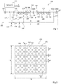
- the figure 1 is a sectional, partial and schematic view of an embodiment of an electronic chip 100.
- the chip 100 preferably comprises a semiconductor substrate 102, for example made of silicon.
- the substrate 102 is for example doped of type P.
- the chip includes chip circuits to protect against attack.
- the circuits comprise for example semiconductor components such as transistors 104.
- the transistors 104 are preferably formed in and on juxtaposed boxes 106 and 108 of alternating conductivity types.
- the boxes 106 and 108 extend into the substrate 102 from its upper face (located on the side of the front face of the chip).
- the chip also comprises a buried box 110, for example doped with type N.
- the box N 110 is located under the boxes 106 and 108.
- the box N 110 is surmounted, for example at its periphery, by contact zones 112 and 114
- the contact areas 112 and 114 are for example N-type doped wells which extend vertically from the front face of the substrate to the N well 110.
- the contact area 112 is connected, for example connected, to a node for applying a bias potential of the box 110, for example a high supply potential VDD.
- the buried caisson 110 is separated from the caissons 106 and 108 by a P-type doped region 120 situated on the buried caisson 110.
- the P region 120 is in contact with the caisson N 110 and thus forms with it a PN 122 junction.
- the region P 120 extends to the front face of the substrate outside the wells 106 and 108.
- Contact areas 124 and 126 with the region P 120 are located outside the wells 106 and 108 The contact areas 124 and 126 are preferably more heavily doped P-type areas than the P region 120.
- the contact area 124 is connected to a circuit 130 (DETECT).
- the circuit 130 emits a signal A as a function of the potential difference between the contact areas 124 and 126.
- the circuit 130 is preferably integrated in and on the chip.
- the contact area 126 is connected to a node for applying a bias potential of the region 120, for example a reference potential such as that of the GND ground.
- the signal A can then be obtained by comparison with a threshold Th1 of the difference between the potential of the area 124 and the bias potential.
- the signal A assumes a high logic level when the potential of the contact area 124 is greater than the threshold Th1.
- Signal A can take a low logic level when this potential is below the threshold Th1.
- the potential of the region 120 remains of the order of that of the GND ground, and the signal A has the low logic level.
- the laser During an attempt to attack from the rear side by means of a laser beam 140, the laser generates a current 142 through the PN junction 122. The current 142 then flows towards the contact area 126 connected to ground. . The passage of current 142 in region 120, due to the electrical resistance of this region, causes a difference in potential between the contact zones 124 and 126.
- the doping levels and the arrangement of the regions 110 and 120 and of the zones 124 and 126, as well as the threshold Th1 are provided so that this potential difference then exceeds the threshold Th1 , taking into account the properties of the laser beam used.
- the laser beam has a wavelength between 900 nm and 1200 nm, an intensity for example between 50 mW and 2000 mW, and a diameter for example between 1 micrometer and 30 micrometers.
- Signal A goes to the high logic level, thus corresponding to the detection of an attack.
- the chip can thus be provided to verify, during startup and / or in operation, that the value of signal A is the low logic level. This makes it possible to verify the absence of an attack.
- the chip can be designed to take any usual countermeasure to counter the attack, such as stopping its operation or destroying information wished by the attacker.
- the region of the substrate 102 located under the box 110 extends outside of the plumb of the box 110 to the front face of the substrate.
- Contact zones 162 and 164 with the region 160 are located outside of the plumb of the box 110.
- the contact zone 164 is connected to a circuit 130.
- the circuit 130 emits a signal A as a function of the potential difference between the contact areas 164 and 162.
- the contact area 162 is connected to ground.
- the signal A assumes a high logic level when the potential of the contact area 164 is greater than a threshold Th2.
- Signal A can take a low logic level when this potential is below the Th2 threshold.
- the operation is similar to that of the first embodiment.
- a current 144 flows through the PN junction between the box 110 and the region 160.
- the current reaches the contact zone 162 connected to ground. Due to the resistance of the substrate, a potential difference ensues between the contact zones 164 and 162, and the signal A changes to the high logic value.
- the first and second embodiments can be combined.
- the chip then comprises both contact zones 124 and 126 with the region 120, and contact zones 162 and 164 with the region 160.
- the contact zones 124 and 164 are connected to the circuit 130.
- the circuit 130 puts the signal A at a high level if at least one of the potentials of the contact areas 124 and 164 becomes greater than the respective threshold Th1, Th2.
- Thresholds Th1 and Th2 can have the same value.
- the circuit 130 gives the signal A a value corresponding to the detection of an attack, for example a high logic level.
- the stack of the region P 160, of the well N 110 and of the region P 120 forms a transistor. As soon as the potential of region 160 in contact with the box 110 exceeds the potential VDD (to the PN junction threshold voltage near), this transistor becomes conducting, and a current 146 passes from region 160 to region 120. This current joins the contact zone 126, and the resistance of the region 120 causes an increase in the potential of the zone 124, which makes it possible to detect the attack.
- the contact zone 114 with the buried box 110 is preferably connected to the circuit 130.
- the circuit 130 provides besides a signal A1 as a function of the potential difference between the contact area 114 and the contact area 112 (connected to the high potential application node VDD).
- the signal A1 has a high logic level when the potential of the contact area 114 is greater than a threshold Th3, and a low logic level when the contact area 114 has its potential less than the threshold Th3.
- the threshold Th3 is for example between the potential of the ground and the potential VDD.
- the circuit 130 supplies the signal A1 as a function of the potential difference between two contact zones 114 with the buried box 110.
- the potential of the region 120 is of the order of VDD, and the signal A1 has the high logic level.
- the potential of the contact zone 114 becomes lower than the potential VDD.
- a current 148 then flows from the box 110 to the region 160. This current comes from the contact area 112 at the potential VDD, and causes, due to the resistance of the box 110, a potential difference within the box 110. It is possible to also provide that this potential difference is related to the depletion of a part of the box N 110 located between the contact zones 112 and 114.
- the signal A1 goes to the low logic level, which thus corresponds to the detection of an attack. .
- the chip is designed to take any countermeasures to counter the attack.
- the chip is designed to take one or more countermeasures when the signal A is at the high logic level as well as when the signal A1 is at the low logic level. This protects the chip against any attack by the back side by laser or by applying a high positive or negative potential on the back side.
- the contact areas 112 and 114 can be pads which are disjoint from each other.
- the contact areas 112 and 114 are parts of an N-type doped peripheral annular wall.
- the annular wall is for example situated on and in contact with the periphery of the box 110.
- the region P 120 is then by example isolated from the region P 160 by the annular wall and therefore defines a box P.
- the boxes 106 and 108 are located in one or more parts 170 of the chip.
- two parts 170 are shown, and, in each part 170, three N-type doped wells 106 are alternated with two P-type 108 wells.
- a number of wells different from that shown is possible, for example only one box 108.
- the number of boxes 106 and 108 can be high, for example more than 100.
- the area 126 can be located between two parts 170 or surrounded by a part 170.
- the contact area 124 is located between two parts 170 or surrounded by a part 170.
- the chip comprises a buried caisson 172 situated under and in contact with some of the caissons 106 and 108.
- the buried caisson 110 is located under the assembly of one of the parts 170.
- the puce can include several buried boxes 172, or be devoid of buried boxes 172.
- Each transistor 104 includes doped zones 180 defining its source and its drain.
- Each doped area 180 has a conductivity type opposite to that of the box 106 or 108 in which the doped area is located.
- such a PN junction can be formed by any component, such as a diode or a thyristor, comprising doped zones located in the box and having a conductivity type opposite to that of the box.
- the wells 106 and 108 reach a depth in the substrate 102, for example between about 0.5 micrometer and about 2 micrometers, for example about 1 micrometer.
- the buried box 172 preferably has a thickness of between around 0.5 micrometer and around 2 micrometers, for example around 1 micrometer.
- the buried box is preferably located at depths of the order of a few micrometers.
- the buried box 110 preferably has a higher level situated at a depth of, for example, between about 3 micrometers and about 10 micrometers, for example between 3 micrometers and 10 micrometers.
- the buried box preferably has a thickness of between around 1 micrometer and around 4 micrometers, for example between 1 micrometer and 4 micrometers.
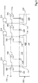
- the figure 2 is a partial and schematic top view of an embodiment of an electronic chip.
- the chip of the figure 2 includes elements identical or similar to those of the chip of the figure 1 , arranged identically or similarly.
- the chip comprises several buried boxes 110, preferably arranged in a matrix.
- Nine boxes 110 are shown by way of example, other numbers of boxes 110 being possible.
- each box 110 seen from above has a rectangular or square shape.
- the distances d1 separating the neighboring wells are preferably between 2 micrometers and 4 micrometers, for example of the order of 3 micrometers.
- the distances d1 are represented at a exaggerated scale compared to that of the boxes 110 and the substrate 102.
- the portion of substrate 102 comprising the boxes 110 has for example a length L and a width W.
- the length L is between 0.5 mm and 2 mm, for example of the order of 1 mm.
- the width W is between 0.5 mm and 2 mm, for example of the order of 1 mm.
- the portion of substrate thus defined has the shape of a square.
- the chip comprises several contact zones 124 with the regions 120 covering the regions 110.
- the chip comprises ten contact zones 124 above each buried box 110.
- the contact zones 124 are arranged in staggered rows.
- the adjacent contact areas 124 for example located in the same row, are separated by a distance d2 of between 75 micrometers and 150 micrometers, for example of the order of 100 micrometers.
- the rows are separated by a distance d3 for example between 30 micrometers and 70 micrometers, for example of the order of 50 micrometers.
- the contact areas 124 have a top view, for example in the form of squares.
- the length d4 of the sides of the squares is between 2 micrometers and 4 micrometers, for example of the order of 3 micrometers.
- the lengths d4 are shown on an exaggerated scale compared to that of the boxes 110 and the substrate 102.
- Each contact area 124 is connected to the circuit 130, not shown in figure 2 .
- the circuit 130 is configured to give the signal A a value corresponding to an attack detection when the potential of at least one of the zones 124 is greater than a threshold. We can thus detect attacks that occur at any position on the rear face.
- the pads 124 and the distances between buried boxes 110 make it possible to protect the circuits of the chip by using a particularly small substrate surface, for example less than 3% of the surface of the substrate.
- the figure 3 shows schematically and in section a part of an embodiment of an electronic chip associated with an example of circuit 130.
- the chip of the figure 3 includes elements identical or similar to those of the chip of the figure 1 , arranged identically or similarly.
- the chip comprises several buried boxes 110.
- the chip comprises for example several contact zones 164 with the regions 160 of the substrate 102 situated under the boxes 110. Some of the contact zones 164 may be located between the boxes 110 neighbors.
- the chip comprises several contact zones 124 with the region 120 situated above each buried box 110.
- Circuit 130 includes a chain of OR 300 logic gates.
- Each OR gate 300 has first and second inputs.
- Each OR gate 300 other than the last gate of the chain has its output connected, for example connected, to the first input of the following OR gate.
- the first input of the first OR gate of the chain is connected to a node '0' for applying a low logic level, for example ground.
- the last OR gate of the chain supplies the signal A.
- Each of the contact zones 164 and 124 is connected, for example connected, to one of the second inputs of the OR gates 300.
- the signal A thus obtained goes to the high logic level as soon as the potential of only one of the contact zones 124 or 164 exceeds a threshold.
- This threshold is here included between the potentials of the low and high logic levels. We thus detect attacks from various positions on the rear side.
- the OR logic gates 300 can then be arranged so as to avoid tracks connecting each contact area to the same place on the chip, for example tracks connecting the contact areas to the inputs of a common OR gate. .
- the chip further comprises several contact zones 114 with the buried caissons 110, where appropriate on each buried caisson 110.
- the contact zones 114 are for example distributed around the periphery of the buried caisson 110.
- the circuit 130 can then further comprise a chain of ET 310 logic gates.
- Each AND gate 310 has a first and a second input.
- Each AND gate 310 other than the last door in the chain has its output connected, for example connected, to the first input of the next AND gate.
- the first input of the first AND gate of the chain is connected to a node '1' for applying a high logic level, for example the potential VDD.
- the last AND gate of the chain provides the signal A1.
- Each of the contact areas 114 is connected, for example connected, to one of the second inputs of the AND doors 310.
- the signal A1 thus obtained goes to the low logic level as soon as the potential of only one of the contact zones 114 is below a threshold. Attacks are thus detected by applying a high negative potential to various positions on the rear face.
Landscapes
- Engineering & Computer Science (AREA)
- Computer Security & Cryptography (AREA)
- Physics & Mathematics (AREA)
- General Physics & Mathematics (AREA)
- Theoretical Computer Science (AREA)
- Computer Networks & Wireless Communication (AREA)
- Signal Processing (AREA)
- Semiconductor Integrated Circuits (AREA)
- Metal-Oxide And Bipolar Metal-Oxide Semiconductor Integrated Circuits (AREA)
Abstract
Description
- La présente description concerne de façon générale les puces électroniques, ou puces de circuit intégré, et en particulier la protection d'une puce contre des attaques.
- Des puces contenant des informations dont l'accès est réservé à des personnes autorisées, telles que des puces de carte bancaire, sont susceptibles d'être la cible d'attaques.
- Divers types d'attaques peuvent être menées à partir de la face arrière d'une puce, opposée à celle où sont situés des circuits contenant les informations. Dans un type d'attaque par la face arrière, l'attaquant perturbe le fonctionnement des circuits, au moyen d'un laser ou par application contre la face arrière d'une sonde portée à une tension élevée. Dans ce dernier cas, le potentiel de la sonde peut être positif ou négatif, par exemple supérieur à plusieurs dizaines de volts, par exemple supérieur à de l'ordre de 50 V. L'attaquant déduit alors les informations convoitées de l'effet de ces perturbations, couramment appelées "fautes".
- Un mode de réalisation pallie tout ou partie des inconvénients des puces électroniques connues.
- Un mode de réalisation pallie tout ou partie des inconvénients des dispositifs connus de protection contre des attaques.
- Un mode de réalisation prévoit une puce électronique comprenant :
- un premier caisson à l'intérieur duquel est située une première jonction PN ;
- un deuxième caisson enterré au-dessous et disjoint du premier caisson ;
- une première région formant une deuxième jonction PN avec le deuxième caisson ; et
- un circuit pour fournir un premier signal en fonction d'au moins une différence de potentiel au sein de la première région.
- Selon un mode de réalisation, la première région est située au moins en partie sous le deuxième caisson.
- Selon un mode de réalisation, la première région est située sur le deuxième caisson.
- Selon un mode de réalisation, la puce comprend au moins une zone de contact avec la première région, reliée audit circuit.
- Selon un mode de réalisation, ledit circuit est configuré pour comparer un potentiel de la zone de contact avec la première région à un potentiel de polarisation de la première région.
- Selon un mode de réalisation, ledit circuit est configuré pour fournir un signal logique.
- Selon un mode de réalisation, la puce comprend une deuxième région dopée formant une troisième jonction PN avec le deuxième caisson, le circuit étant configuré pour que le premier signal soit en outre fonction d'au moins une différence de potentiel au sein de la deuxième région.
- Selon un mode de réalisation, la deuxième région est située sous et autour du deuxième caisson.
- Selon un mode de réalisation, ledit circuit est configuré pour comparer un potentiel d'une zone de contact avec la deuxième région à un potentiel de polarisation de la deuxième région.
- Selon un mode de réalisation, le circuit est configuré pour fournir en outre un deuxième signal en fonction d'au moins une différence de potentiel au sein du deuxième caisson.
- Selon un mode de réalisation, ledit circuit est configuré pour comparer un potentiel d'une zone de contact avec le deuxième caisson à un potentiel de polarisation du deuxième caisson.
- Selon un mode de réalisation, la zone de contact avec le deuxième caisson s'étend verticalement sur et à partir d'une partie périphérique du deuxième caisson.
- Selon un mode de réalisation, la zone de contact avec le deuxième caisson forme sur le deuxième caisson un mur annulaire périphérique.
- Selon un mode de réalisation, la zone de contact avec le premier caisson forme un plot sur le deuxième caisson.
- Selon un mode de réalisation, la puce comprend en outre un caisson enterré supplémentaire, situé au-dessus et disjoint du deuxième caisson, formant une jonction PN supplémentaire avec le premier caisson.
- Un mode de réalisation prévoit un procédé de détection d'attaque d'une puce électronique, dans lequel un niveau logique du premier signal correspond à une absence d'attaque.
- Selon un mode de réalisation, un niveau logique du deuxième signal correspond à une absence d'attaque.
- Ces caractéristiques et avantages, ainsi que d'autres, seront exposés en détail dans la description suivante de modes de réalisation particuliers faite à titre non limitatif en relation avec les figures jointes parmi lesquelles :
- la
figure 1 est une vue en coupe, partielle et schématique, d'un mode de réalisation d'une puce électronique ; - la
figure 2 est une vue de dessus partielle et schématique d'un mode de réalisation d'une puce électronique ; et - la
figure 3 représente schématiquement et en coupe une partie d'un mode de réalisation d'une puce électronique associée à un circuit de détection. - De mêmes éléments ont été désignés par de mêmes références dans les différentes figures. En particulier, les éléments structurels et/ou fonctionnels communs aux différents modes de réalisation peuvent présenter les mêmes références et peuvent disposer de propriétés structurelles, dimensionnelles et matérielles identiques.
- Par souci de clarté, seuls les étapes et éléments utiles à la compréhension des modes de réalisation décrits ont été représentés et sont détaillés. En particulier, des circuits de puce électronique ne sont pas représentés, les modes de réalisation décrits étant compatibles avec la plupart des circuits courants.
- Sauf précision contraire, lorsque l'on fait référence à deux éléments connectés entre eux, cela signifie directement connectés sans éléments intermédiaires autres que des conducteurs, et lorsque l'on fait référence à deux éléments reliés ou couplés entre eux, cela signifie que ces deux éléments peuvent être connectés ou être reliés ou couplés par l'intermédiaire d'un ou plusieurs autres éléments.
- Dans la description qui suit, lorsque l'on fait référence à des qualificatifs de position absolue, tels que les termes "haut", "bas", "gauche", "droite", etc., ou relative, tels que les termes "dessus", "dessous", "supérieur", "inférieur", etc., ou à des qualificatifs d'orientation, tels que les termes "horizontal", "vertical", etc., il est fait référence sauf précision contraire à l'orientation des vues en coupe dans les figures.
- Sauf précision contraire, les expressions "environ", "approximativement", "sensiblement", et "de l'ordre de" signifient à 10 % près, de préférence à 5 % près.
- La
figure 1 est une vue en coupe, partielle et schématique, d'un mode de réalisation d'une puce électronique 100. - La puce 100 comprend de préférence un substrat semiconducteur 102, par exemple en silicium. Le substrat 102 est par exemple dopé de type P.
- La puce comprend des circuits de la puce à protéger contre les attaques. Les circuits comprennent par exemple des composants semiconducteurs tels que des transistors 104. Les transistors 104 sont de préférence formés dans et sur des caissons 106 et 108 juxtaposés de types de conductivité alternés. Les caissons 106 et 108 s'étendent dans le substrat 102 à partir de sa face supérieure (située du côté de la face avant de la puce).
- La puce comprend en outre un caisson enterré 110, par exemple dopé de type N. Le caisson N 110 est situé sous les caissons 106 et 108. Le caisson N 110 est surmonté, par exemple à sa périphérie, de zones de contact 112 et 114. Les zones de contact 112 et 114 sont par exemple des caissons dopés de type N qui s'étendent verticalement de la face avant du substrat au caisson N 110. De préférence, la zone de contact 112 est reliée, par exemple connectée, à un noeud d'application d'un potentiel de polarisation du caisson 110, par exemple un potentiel haut d'alimentation VDD.
- Le caisson enterré 110 est séparé des caissons 106 et 108 par une région 120 dopée de type P située sur le caisson enterré 110. La région P 120 est en contact avec le caisson N 110 et forme ainsi avec lui une jonction PN 122.
- Dans un premier mode de réalisation, la région P 120 se prolonge jusqu'à la face avant du substrat en dehors des caissons 106 et 108. Des zones de contact 124 et 126 avec la région P 120 sont situées en dehors des caissons 106 et 108. Les zones de contact 124 et 126 sont de préférence des zones plus fortement dopées de type P que la région P 120. La zone de contact 124 est reliée à un circuit 130 (DETECT). Le circuit 130 émet un signal A en fonction de la différence de potentiel entre les zones de contact 124 et 126. Le circuit 130 est de préférence intégré dans et sur la puce.
- De préférence, la zone de contact 126 est connectée à un noeud d'application d'un potentiel de polarisation de la région 120, par exemple un potentiel de référence tel que celui de la masse GND. Le signal A peut alors être obtenu par comparaison à un seuil Th1 de la différence entre le potentiel de la zone 124 et le potentiel de polarisation. A titre d'exemple, le signal A prend un niveau logique haut lorsque le potentiel de la zone de contact 124 est supérieur au seuil Th1. Le signal A peut prendre un niveau logique bas lorsque ce potentiel est inférieur au seuil Th1.
- En l'absence d'attaque, le potentiel de la région 120 reste de l'ordre de celui de la masse GND, et le signal A a le niveau logique bas.
- Lors d'une tentative d'attaque par la face arrière au moyen d'un faisceau laser 140, le laser génère un courant 142 à travers la jonction PN 122. Le courant 142 se dirige alors vers la zone de contact 126 reliée à la masse. Le passage du courant 142 dans la région 120, du fait de la résistance électrique de cette région, provoque une différence de potentiel entre les zones de contact 124 et 126. Les niveaux de dopage et l'agencement des régions 110 et 120 et des zones 124 et 126, ainsi que le seuil Th1, sont prévus de sorte que cette différence de potentiel dépasse alors le seuil Th1, compte tenu des propriétés du faisceau laser utilisé. A titre d'exemple, le faisceau laser a une longueur d'onde comprise entre 900 nm et 1200 nm, une intensité par exemple comprise entre 50 mW et 2000 mW, et un diamètre par exemple compris entre 1 micromètre et 30 micromètres. Le signal A passe au niveau logique haut, correspondant ainsi à la détection d'une attaque.
- La puce peut ainsi être prévue pour vérifier, en cours de démarrage et/ou en fonctionnement, que la valeur du signal A est le niveau logique bas. Ceci permet de vérifier l'absence d'attaque. Lorsqu'une attaque provoque le passage au niveau logique haut du signal A, la puce peut être prévue pour prendre toute contre-mesure usuelle pour contrer l'attaque, telle que stopper son fonctionnement ou détruire des informations convoitées par l'attaquant.
- Dans un deuxième mode de réalisation, la région du substrat 102 située sous le caisson 110 (région 160) se prolonge en dehors de l'aplomb du caisson 110 jusqu'à la face avant du substrat. Des zones de contact 162 et 164 avec la région 160 sont situées en dehors de l'aplomb du caisson 110. La zone de contact 164 est reliée à un circuit 130. Le circuit 130 émet un signal A en fonction de la différence de potentiel entre les zones de contact 164 et 162. De préférence, la zone de contact 162 est reliée à la masse. A titre d'exemple, le signal A prend un niveau logique haut lorsque le potentiel de la zone de contact 164 est supérieur à un seuil Th2. Le signal A peut prendre un niveau logique bas lorsque ce potentiel est inférieur au seuil Th2.
- Le fonctionnement est similaire à celui du premier mode de réalisation. En cas d'attaque par la face arrière par un laser 140, un courant 144 s'écoule à travers la jonction PN entre le caisson 110 et la région 160. Le courant rejoint la zone de contact 162 reliée à la masse. Du fait de la résistance du substrat, il s'ensuit une différence de potentiel entre les zones de contact 164 et 162, et le signal A passe à la valeur logique haute.
- Les premier et deuxième modes de réalisation peuvent être combinés. La puce comprend alors à la fois des zones de contact 124 et 126 avec la région 120, et des zones de contact 162 et 164 avec la région 160. Les zones de contact 124 et 164 sont reliées au circuit 130. Le circuit 130 met le signal A à un niveau haut si au moins l'un des potentiels des zones de contact 124 et 164 devient supérieur au seuil respectif Th1, Th2. Les seuils Th1 et Th2 peuvent avoir la même valeur.
- En cas d'attaque par application d'un potentiel positif sur la face arrière de la puce, le potentiel de la zone de contact 164 s'élève, tandis que celui de la région 162 reste le potentiel nul de la masse. De ce fait, le circuit 130 donne au signal A une valeur correspondant à la détection d'une attaque, par exemple un niveau logique haut. De plus, l'empilement de la région P 160, du caisson N 110 et de la région P 120 forme un transistor. Dès que le potentiel de la région 160 au contact du caisson 110 dépasse le potentiel VDD (à la tension de seuil de jonction PN près), ce transistor devient passant, et un courant 146 passe de la région 160 à la région 120. Ce courant rejoint la zone de contact 126, et la résistance de la région 120 provoque une élévation du potentiel de la zone 124, ce qui permet de détecter l'attaque.
- Dans les modes de réalisation décrits ci-dessus, la zone de contact 114 avec le caisson enterré 110 est de préférence reliée au circuit 130. Le circuit 130 fournit en outre un signal A1 en fonction de la différence de potentiel entre la zone de contact 114 et la zone de contact 112 (reliée au noeud d'application du potentiel haut VDD). A titre d'exemple, le signal A1 a un niveau logique haut lorsque le potentiel de la zone de contact 114 est supérieur à un seuil Th3, et un niveau logique bas lorsque la zone de contact 114 a son potentiel inférieur au seuil Th3. Le seuil Th3 est par exemple compris entre le potentiel de la masse et le potentiel VDD. A titre de variante, le circuit 130 fournit le signal A1 en fonction de la différence de potentiel entre deux zones de contact 114 avec le caisson enterré 110.
- En l'absence d'attaque, le potentiel de la région 120 est de l'ordre de VDD, et le signal A1 a le niveau logique haut.
- En cas d'attaque par application d'un potentiel négatif élevé sur la face arrière, le potentiel de la zone de contact 114 devient inférieur au potentiel VDD. Pour cela, on peut prévoir que la jonction PN entre le caisson 110 et la région 160 entre en avalanche en cas d'une telle attaque. Un courant 148 circule alors du caisson 110 à la région 160. Ce courant provient de la zone de contact 112 au potentiel VDD, et provoque, du fait de la résistance du caisson 110, une différence de potentiel au sein du caisson 110. On peut aussi prévoir que cette différence de potentiel soit liée à la déplétion d'une partie du caisson N 110 située entre les zones de contact 112 et 114. Le signal A1 passe au niveau logique bas, ce qui correspond ainsi à la détection d'une attaque. La puce est prévue pour prendre alors toute contre-mesure permettant de contrer l'attaque.
- De préférence, la puce est prévue pour prendre une ou des contre-mesures lorsque le signal A est au niveau logique haut ainsi que lorsque le signal A1 est au niveau logique bas. Ceci permet de protéger la puce contre toute attaque par la face arrière par laser ou par application d'un potentiel positif ou négatif élevé sur la face arrière.
- Les zones de contact 112 et 114 peuvent être des plots disjoints les uns des autres. Dans une variante, les zones de contact 112 et 114 sont des parties d'un mur annulaire périphérique dopé de type N. Le mur annulaire est par exemple situé sur et en contact avec la périphérie du caisson 110. La région P 120 est alors par exemple isolée de la région P 160 par le mur annulaire et définit donc un caisson P.
- Dans l'exemple représenté en
figure 1 , les caissons 106 et 108 sont situés dans une ou plusieurs parties 170 de la puce. A titre illustratif, deux parties 170 sont représentées, et, dans chaque partie 170, trois caissons 106 dopés de type N sont alternés avec deux caissons 108 dopés de type P. Un nombre de caissons différent de celui représenté est possible, par exemple un seul caisson 108. En pratique, le nombre de caissons 106 et 108 peut être élevé, par exemple supérieur à 100. La zone 126 peut être située entre deux parties 170 ou entourée d'une partie 170. A titre de variante, la zone de contact 124 est située entre deux parties 170 ou entourée d'une partie 170. - A titre d'exemple, la puce comprend un caisson enterré 172 situé sous et en contact avec certains des caissons 106 et 108. Dans l'exemple illustré, le caisson enterré 110 est situé sous l'ensemble d'une des parties 170. La puce peut comprendre plusieurs caissons enterrés 172, ou être dépourvue de caisson enterré 172.
- Chaque transistor 104 comprend des zones dopées 180 définissant sa source et son drain. Chaque zone dopée 180 a un type de conductivité opposé à celui du caisson 106 ou 108 dans lequel la zone dopée est située. Ceci forme une jonction PN dans le caisson 106 ou 108 concerné. A titre de variante, une telle jonction PN peut être formée par tout composant, tel qu'une diode ou un thyristor, comprenant des zones dopées situées dans le caisson et ayant un type de conductivité opposé à celui du caisson.
- De préférence, les caissons 106 et 108 atteignent dans le substrat 102 une profondeur par exemple comprise entre de l'ordre de 0,5 micromètre et de l'ordre de 2 micromètres, par exemple de l'ordre de 1 micromètre. Le caisson enterré 172 a de préférence une épaisseur comprise entre de l'ordre de 0,5 micromètre et de l'ordre de 2 micromètres, par exemple de l'ordre de 1 micromètre. Le caisson enterré est de préférence situé à des profondeurs de l'ordre de quelques micromètres. Le caisson enterré 110 a de préférence un niveau supérieur situé à une profondeur comprise par exemple entre de l'ordre de 3 micromètres et de l'ordre de 10 micromètres, par exemple entre 3 micromètres et 10 micromètres. Le caisson enterré a de préférence une épaisseur comprise entre de l'ordre de 1 micromètre et de l'ordre de 4 micromètres, par exemple entre 1 micromètre et 4 micromètres.
- La
figure 2 est une vue de dessus partielle et schématique d'un mode de réalisation d'une puce électronique. La puce de lafigure 2 comprend des éléments identiques ou similaires à ceux de la puce de lafigure 1 , agencés de manière identique ou similaire. - Dans une portion du substrat 102, la puce comprend plusieurs caissons enterrés 110, de préférence disposés en matrice. Neuf caissons 110 sont représentés à titre d'exemple, d'autres nombres de caissons 110 étant possibles. De préférence, chaque caisson 110 vu de dessus a une forme rectangulaire ou carrée. Les distances d1 séparant les caissons voisins sont de préférence comprises entre 2 micromètres et 4 micromètres, par exemple de l'ordre de 3 micromètres. Les distances d1 sont représentées à une échelle exagérée par rapport à celle des caissons 110 et du substrat 102.
- La portion de substrat 102 comprenant les caissons 110 a par exemple une longueur L et une largeur W. De préférence, la longueur L est comprise entre 0,5 mm et 2 mm, par exemple de l'ordre de 1 mm. De préférence, la largeur W est comprise entre 0,5 mm et 2 mm, par exemple de l'ordre de 1 mm. De préférence, la portion de substrat ainsi définie a la forme d'un carré.
- La puce comprend plusieurs zones de contact 124 avec les régions 120 recouvrant les régions 110. Dans l'exemple illustré, la puce comprend dix zones de contact 124 au-dessus de chaque caisson enterré 110. A titre d'exemple, les zones de contact 124 sont disposées en quinconce selon des rangées. De préférence, les zones de contact 124 voisines, par exemple situées dans une même rangée, sont séparées d'une distance d2 comprise entre 75 micromètres et 150 micromètres, par exemple de l'ordre de 100 micromètres. Les rangées sont séparées d'une distance d3 par exemple comprise entre 30 micromètres et 70 micromètres, par exemple de l'ordre de 50 micromètres. Les zones de contact 124 ont en vue de dessus par exemple la forme de carrés. De préférence, la longueur d4 des côtés des carrés est comprise entre 2 micromètres et 4 micromètres, par exemple de l'ordre de 3 micromètres. Les longueurs d4 sont représentées à une échelle exagérée par rapport à celle des caissons 110 et du substrat 102.
- Chaque zone de contact 124 est reliée au circuit 130, non représenté en
figure 2 . De préférence, le circuit 130 est configuré pour donner au signal A une valeur correspondant à une détection d'attaque lorsque le potentiel d'au moins une des zones 124 est supérieur à un seuil. On peut ainsi détecter les attaques qui se produisent à n'importe quelle position sur la face arrière. - Selon un avantage, les plots 124 et les distances entre caissons enterrés 110 permettent de protéger les circuits de la puce en utilisant une surface de substrat particulièrement faible, par exemple inférieure à 3 % de la surface du substrat.
- La
figure 3 représente schématiquement et en coupe une partie d'un mode de réalisation d'une puce électronique associée à un exemple de circuit 130. La puce de lafigure 3 comprend des éléments identiques ou similaires à ceux de la puce de lafigure 1 , agencés de manière identique ou similaire. - A titre d'exemple, la puce comprend plusieurs caissons enterrés 110. La puce comprend par exemple plusieurs zones de contact 164 avec les régions 160 du substrat 102 situées sous les caissons 110. Certaines des zones de contact 164 peuvent être situées entre les caissons 110 voisins. De préférence, la puce comprend plusieurs zones de contact 124 avec la région 120 située au-dessus de chaque caisson enterré 110.
- Le circuit 130 comprend une chaîne de portes logiques OU 300. Chaque porte OU 300 a une première et une deuxième entrée. Chaque porte OU 300 autre que la dernière porte de la chaîne a sa sortie reliée, par exemple connectée, à la première entrée de la porte OU suivante. La première entrée de la première porte OU de la chaîne est reliée à un noeud '0' d'application d'un niveau logique bas, par exemple la masse. La dernière porte OU de la chaîne fournit le signal A. Chacune des zones de contact 164 et 124 est reliée, par exemple connectée, à une des deuxièmes entrées des portes OU 300.
- Le signal A ainsi obtenu passe au niveau logique haut dès que le potentiel d'une seule des zones de contact 124 ou 164 dépasse un seuil. Ce seuil est ici compris entre les potentiels des niveaux logiques bas et haut. On détecte ainsi les attaques menées à partir de diverses positions sur la face arrière.
- Selon un avantage, les portes logiques OU 300 peuvent alors être disposées en sorte d'éviter des pistes reliant chaque zone de contact à un même endroit de la puce, par exemple des pistes reliant les zones de contact aux entrées d'une porte OU commune.
- De préférence, la puce comprend en outre plusieurs zones de contact 114 avec les caissons enterrés 110, le cas échéant sur chaque caisson enterré 110. Les zones de contact 114 sont par exemple réparties à la périphérie du caisson enterré 110.
- Le circuit 130 peut alors comprendre en outre une chaîne de portes logiques ET 310. Chaque porte ET 310 a une première et une deuxième entrée. Chaque porte ET 310 autre que la dernière porte de la chaîne a sa sortie reliée, par exemple connectée, à la première entrée de la porte ET suivante. La première entrée de la première porte ET de la chaîne est reliée à un noeud '1' d'application d'un niveau logique haut, par exemple le potentiel VDD. La dernière porte ET de la chaîne fournit le signal A1. Chacune des zones de contact 114 est reliée, par exemple connectée, à une des deuxièmes entrées des portes ET 310.
- Le signal A1 ainsi obtenu passe au niveau logique bas dès que le potentiel d'une seule des zones de contact 114 est en deçà d'un seuil. On détecte ainsi les attaques par application d'un potentiel négatif élevé à diverses positions sur la face arrière.
- Divers modes de réalisation et variantes ont été décrits. L'homme de l'art comprendra que certaines caractéristiques de ces divers modes de réalisation et variantes pourraient être combinées, et d'autres variantes apparaitront à l'homme de l'art. En particulier, les types de dopage des modes de réalisation décrits peuvent être inversés en échangeant les sens des différences de potentiel.
- Enfin, la mise en oeuvre pratique des modes de réalisation et variantes décrits est à la portée de l'homme du métier à partir des indications fonctionnelles données ci-dessus.
Claims (17)
- Puce électronique comprenant :un premier caisson (106, 108) à l'intérieur duquel est située une première jonction PN ;un deuxième caisson (110) enterré au-dessous et disjoint du premier caisson ;une première région (120 ; 160) formant une deuxième jonction PN avec le deuxième caisson ; etun circuit (130) pour fournir un premier signal (A) en fonction d'au moins une différence de potentiel au sein de la première région.
- Puce électronique selon la revendication 1, dans laquelle la première région (160) est située au moins en partie sous le deuxième caisson (110).
- Puce électronique selon la revendication 1, dans laquelle la première région (160) est située sur le deuxième caisson (110) .
- Puce électronique selon l'une quelconque des revendications 1 à 3, comprenant au moins une zone de contact avec la première région (124 ; 164), reliée audit circuit (130).
- Puce électronique selon la revendication 4, dans laquelle ledit circuit (130) est configuré pour comparer un potentiel de la zone de contact avec la première région (124 ; 164) à un potentiel de polarisation de la première région (GND).
- Puce électronique selon la revendication 5, dans laquelle ledit circuit (130) est configuré pour fournir un signal logique (A) .
- Puce électronique selon l'une quelconque des revendications 1 à 6, comprenant une deuxième région (160) dopée formant une troisième jonction PN avec le deuxième caisson (110), le circuit (130) étant configuré pour que le premier signal (A) soit en outre fonction d'au moins une différence de potentiel au sein de la deuxième région.
- Puce électronique selon la revendication 7, dans laquelle la deuxième région (160) est située sous et autour du deuxième caisson (110).
- Puce électronique selon la revendication 7 ou 8, dans laquelle ledit circuit est configuré pour comparer un potentiel d'une zone de contact avec la deuxième région (164) à un potentiel de polarisation de la deuxième région (GND).
- Puce électronique selon l'une quelconque des revendications 1 à 9, dans laquelle le circuit (130) est configuré pour fournir en outre un deuxième signal (A1) en fonction d'au moins une différence de potentiel au sein du deuxième caisson (110).
- Puce électronique selon la revendication 10, dans laquelle ledit circuit (130) est configuré pour comparer un potentiel d'une zone de contact avec le deuxième caisson (114) à un potentiel de polarisation du deuxième caisson (VDD).
- Puce électronique selon la revendication 11, dans laquelle la zone de contact avec le deuxième caisson (114) s'étend verticalement sur et à partir d'une partie périphérique du deuxième caisson (110).
- Puce électronique selon la revendication 12, dans laquelle la zone de contact avec le deuxième caisson (114) forme sur le deuxième caisson (110) un mur annulaire périphérique.
- Puce électronique selon la revendication 12, dans laquelle la zone de contact avec le premier caisson (114) forme un plot sur le deuxième caisson (110).
- Puce électronique selon l'une quelconque des revendications 1 à 14, comprenant en outre un caisson enterré supplémentaire (172), situé au-dessus et disjoint du deuxième caisson (110), formant une jonction PN supplémentaire avec le premier caisson (108) .
- Procédé de détection d'attaque d'une puce électronique selon l'une quelconque des revendications 1 à 15, dans lequel un niveau logique du premier signal (A) correspond à une absence d'attaque.
- Procédé selon la revendication 16 dans son rattachement à la revendication 10, dans lequel un niveau logique du deuxième signal (A1) correspond à une absence d'attaque.
Applications Claiming Priority (1)
| Application Number | Priority Date | Filing Date | Title |
|---|---|---|---|
| FR1856507A FR3083919A1 (fr) | 2018-07-13 | 2018-07-13 | Puce electronique protegee |
Publications (2)
| Publication Number | Publication Date |
|---|---|
| EP3594999A1 true EP3594999A1 (fr) | 2020-01-15 |
| EP3594999B1 EP3594999B1 (fr) | 2025-04-09 |
Family
ID=65494190
Family Applications (1)
| Application Number | Title | Priority Date | Filing Date |
|---|---|---|---|
| EP19184586.6A Active EP3594999B1 (fr) | 2018-07-13 | 2019-07-05 | Puce électronique protégée |
Country Status (3)
| Country | Link |
|---|---|
| US (1) | US11011479B2 (fr) |
| EP (1) | EP3594999B1 (fr) |
| FR (1) | FR3083919A1 (fr) |
Citations (2)
| Publication number | Priority date | Publication date | Assignee | Title |
|---|---|---|---|---|
| EP3159872A1 (fr) * | 2015-10-22 | 2017-04-26 | Stmicroelectronics (Rousset) Sas | Puce électronique sécurisée au moyen de de multiple caissons |
| EP3236496A1 (fr) * | 2016-04-19 | 2017-10-25 | Stmicroelectronics (Rousset) Sas | Puce électronique protégée contre des attaques en face arrière |
Family Cites Families (8)
| Publication number | Priority date | Publication date | Assignee | Title |
|---|---|---|---|---|
| IT1231894B (it) * | 1987-10-15 | 1992-01-15 | Sgs Microelettronica Spa | Dispositivo integrato per schermare l'iniezione di cariche nel substrato. |
| IT1252623B (it) * | 1991-12-05 | 1995-06-19 | Sgs Thomson Microelectronics | Dispositivo a semiconduttore comprendente almeno un transistor di potenza e almeno un circuito di comando, con circuito di isolamento dinamico,integrati in maniera monolitica nella stessa piastrina |
| EP0734070B1 (fr) * | 1995-03-22 | 2000-07-19 | Consorzio per la Ricerca sulla Microelettronica nel Mezzogiorno - CoRiMMe | Procédé et dispositif pour autopolariser dynamiquement des régions de circuits intégrés |
| EP0847089B1 (fr) * | 1996-12-09 | 2002-10-23 | STMicroelectronics S.r.l. | Méthode et dispositif pour supprimer des effets parasites dans un circuit integré avec des jonctions d'isolation |
| JP3886590B2 (ja) * | 1997-03-12 | 2007-02-28 | 株式会社ルネサステクノロジ | 半導体装置およびその製造方法 |
| US8373497B2 (en) * | 2011-01-11 | 2013-02-12 | Infineon Technologies Ag | System and method for preventing bipolar parasitic activation in a semiconductor circuit |
| JP5935274B2 (ja) * | 2011-09-22 | 2016-06-15 | ソニー株式会社 | 固体撮像装置、固体撮像装置の制御方法および固体撮像装置の制御プログラム |
| FR3057087B1 (fr) * | 2016-09-30 | 2018-11-16 | Stmicroelectronics (Rousset) Sas | Puce electronique protegee |
-
2018
- 2018-07-13 FR FR1856507A patent/FR3083919A1/fr not_active Ceased
-
2019
- 2019-07-05 EP EP19184586.6A patent/EP3594999B1/fr active Active
- 2019-07-05 US US16/503,876 patent/US11011479B2/en active Active
Patent Citations (2)
| Publication number | Priority date | Publication date | Assignee | Title |
|---|---|---|---|---|
| EP3159872A1 (fr) * | 2015-10-22 | 2017-04-26 | Stmicroelectronics (Rousset) Sas | Puce électronique sécurisée au moyen de de multiple caissons |
| EP3236496A1 (fr) * | 2016-04-19 | 2017-10-25 | Stmicroelectronics (Rousset) Sas | Puce électronique protégée contre des attaques en face arrière |
Also Published As
| Publication number | Publication date |
|---|---|
| FR3083919A1 (fr) | 2020-01-17 |
| US11011479B2 (en) | 2021-05-18 |
| EP3594999B1 (fr) | 2025-04-09 |
| US20200020650A1 (en) | 2020-01-16 |
Similar Documents
| Publication | Publication Date | Title |
|---|---|---|
| EP2535932B1 (fr) | Puce de circuit intégré comprenant un dispositif de protection contre des attaques | |
| EP3151290B1 (fr) | Photodiode de type spad | |
| FR2981783A1 (fr) | Systeme de detection d'une attaque par laser d'une puce de circuit integre | |
| EP3301605B1 (fr) | Puce électronique protégée | |
| EP2535933B1 (fr) | Puce de circuit intégré comprenant un dispositif de protection contre des attaques | |
| FR2991083A1 (fr) | Procede et dispositif de protection d'un circuit integre contre des attaques par sa face arriere | |
| EP3159872B1 (fr) | Puce électronique sécurisée au moyen de multiple caissons | |
| FR2986356A1 (fr) | Dispositif de protection d'un circuit integre contre des attaques en face arriere | |
| FR2812972A1 (fr) | Dispositif a semiconducteur consistant en un thyristor pour la protection contre les decharges electrostatiques | |
| FR2998419A1 (fr) | Protection d'un circuit integre contre des attaques | |
| FR2993404A1 (fr) | Circuit integre sur soi comprenant un thyristor (scr) de protection contre des decharges electrostatiques | |
| EP3291293B1 (fr) | Puce protégée contre les attaques face arrière | |
| EP3236496B1 (fr) | Puce électronique protégée contre des attaques en face arrière | |
| EP3016141A1 (fr) | Capteur d'image à électrodes verticales | |
| EP3151277B1 (fr) | Circuit intégré sécurisé | |
| EP3629380A1 (fr) | Structure de diode | |
| EP3594999B1 (fr) | Puce électronique protégée | |
| FR3072211A1 (fr) | Procede de detection d'une injection de fautes et d'un amincissement du substrat dans un circuit integre, et circuit integre associe | |
| EP3373330B1 (fr) | Architecture de puce électronique | |
| EP1691413A1 (fr) | Composant électronique protégé contre les attaques. | |
| FR3057088A1 (fr) | Detecteur laser picosecondes | |
| EP3361498B1 (fr) | Condensateur de découplage | |
| EP3593380A1 (fr) | Puce electronique | |
| FR3069703A1 (fr) | Puce electronique | |
| EP3739622A1 (fr) | Procédé de détection d'une atteinte éventuelle à l'intégrité d'un substrat semi-conducteur d'un circuit intégré depuis sa face arrière, et circuit intégré correspondant |
Legal Events
| Date | Code | Title | Description |
|---|---|---|---|
| PUAI | Public reference made under article 153(3) epc to a published international application that has entered the european phase |
Free format text: ORIGINAL CODE: 0009012 |
|
| STAA | Information on the status of an ep patent application or granted ep patent |
Free format text: STATUS: REQUEST FOR EXAMINATION WAS MADE |
|
| 17P | Request for examination filed |
Effective date: 20190705 |
|
| AK | Designated contracting states |
Kind code of ref document: A1 Designated state(s): AL AT BE BG CH CY CZ DE DK EE ES FI FR GB GR HR HU IE IS IT LI LT LU LV MC MK MT NL NO PL PT RO RS SE SI SK SM TR |
|
| AX | Request for extension of the european patent |
Extension state: BA ME |
|
| RIC1 | Information provided on ipc code assigned before grant |
Ipc: G09C 1/00 20060101ALI20200324BHEP Ipc: H04L 9/00 20060101ALI20200324BHEP Ipc: H01L 23/00 20060101AFI20200324BHEP Ipc: H01L 21/8238 20060101ALI20200324BHEP Ipc: H01L 27/04 20060101ALI20200324BHEP Ipc: H01L 27/092 20060101ALI20200324BHEP Ipc: H01L 23/58 20060101ALI20200324BHEP |
|
| STAA | Information on the status of an ep patent application or granted ep patent |
Free format text: STATUS: EXAMINATION IS IN PROGRESS |
|
| 17Q | First examination report despatched |
Effective date: 20201015 |
|
| REG | Reference to a national code |
Ref country code: DE Ref legal event code: R079 Free format text: PREVIOUS MAIN CLASS: H01L0023000000 Ipc: G09C0001000000 Ref country code: DE Ref legal event code: R079 Ref document number: 602019068335 Country of ref document: DE Free format text: PREVIOUS MAIN CLASS: H01L0023000000 Ipc: G09C0001000000 |
|
| GRAP | Despatch of communication of intention to grant a patent |
Free format text: ORIGINAL CODE: EPIDOSNIGR1 |
|
| STAA | Information on the status of an ep patent application or granted ep patent |
Free format text: STATUS: GRANT OF PATENT IS INTENDED |
|
| RIC1 | Information provided on ipc code assigned before grant |
Ipc: H01L 21/8238 20060101ALN20241120BHEP Ipc: H04L 9/00 20060101ALI20241120BHEP Ipc: H01L 27/04 20060101ALI20241120BHEP Ipc: H01L 27/092 20060101ALI20241120BHEP Ipc: H01L 23/58 20060101ALI20241120BHEP Ipc: G09C 1/00 20060101AFI20241120BHEP |
|
| INTG | Intention to grant announced |
Effective date: 20241205 |
|
| GRAS | Grant fee paid |
Free format text: ORIGINAL CODE: EPIDOSNIGR3 |
|
| GRAA | (expected) grant |
Free format text: ORIGINAL CODE: 0009210 |
|
| STAA | Information on the status of an ep patent application or granted ep patent |
Free format text: STATUS: THE PATENT HAS BEEN GRANTED |
|
| AK | Designated contracting states |
Kind code of ref document: B1 Designated state(s): AL AT BE BG CH CY CZ DE DK EE ES FI FR GB GR HR HU IE IS IT LI LT LU LV MC MK MT NL NO PL PT RO RS SE SI SK SM TR |
|
| REG | Reference to a national code |
Ref country code: GB Ref legal event code: FG4D Free format text: NOT ENGLISH |
|
| REG | Reference to a national code |
Ref country code: CH Ref legal event code: EP |
|
| REG | Reference to a national code |
Ref country code: DE Ref legal event code: R096 Ref document number: 602019068335 Country of ref document: DE |
|
| REG | Reference to a national code |
Ref country code: IE Ref legal event code: FG4D Free format text: LANGUAGE OF EP DOCUMENT: FRENCH |
|
| REG | Reference to a national code |
Ref country code: NL Ref legal event code: MP Effective date: 20250409 |
|
| PG25 | Lapsed in a contracting state [announced via postgrant information from national office to epo] |
Ref country code: NL Free format text: LAPSE BECAUSE OF FAILURE TO SUBMIT A TRANSLATION OF THE DESCRIPTION OR TO PAY THE FEE WITHIN THE PRESCRIBED TIME-LIMIT Effective date: 20250409 |
|
| REG | Reference to a national code |
Ref country code: AT Ref legal event code: MK05 Ref document number: 1784275 Country of ref document: AT Kind code of ref document: T Effective date: 20250409 |
|
| PG25 | Lapsed in a contracting state [announced via postgrant information from national office to epo] |
Ref country code: ES Free format text: LAPSE BECAUSE OF FAILURE TO SUBMIT A TRANSLATION OF THE DESCRIPTION OR TO PAY THE FEE WITHIN THE PRESCRIBED TIME-LIMIT Effective date: 20250409 Ref country code: PT Free format text: LAPSE BECAUSE OF FAILURE TO SUBMIT A TRANSLATION OF THE DESCRIPTION OR TO PAY THE FEE WITHIN THE PRESCRIBED TIME-LIMIT Effective date: 20250811 Ref country code: FI Free format text: LAPSE BECAUSE OF FAILURE TO SUBMIT A TRANSLATION OF THE DESCRIPTION OR TO PAY THE FEE WITHIN THE PRESCRIBED TIME-LIMIT Effective date: 20250409 |
|
| PGFP | Annual fee paid to national office [announced via postgrant information from national office to epo] |
Ref country code: DE Payment date: 20250630 Year of fee payment: 7 |
|
| REG | Reference to a national code |
Ref country code: LT Ref legal event code: MG9D |
|
| PG25 | Lapsed in a contracting state [announced via postgrant information from national office to epo] |
Ref country code: GR Free format text: LAPSE BECAUSE OF FAILURE TO SUBMIT A TRANSLATION OF THE DESCRIPTION OR TO PAY THE FEE WITHIN THE PRESCRIBED TIME-LIMIT Effective date: 20250710 Ref country code: NO Free format text: LAPSE BECAUSE OF FAILURE TO SUBMIT A TRANSLATION OF THE DESCRIPTION OR TO PAY THE FEE WITHIN THE PRESCRIBED TIME-LIMIT Effective date: 20250709 |
|
| PG25 | Lapsed in a contracting state [announced via postgrant information from national office to epo] |
Ref country code: PL Free format text: LAPSE BECAUSE OF FAILURE TO SUBMIT A TRANSLATION OF THE DESCRIPTION OR TO PAY THE FEE WITHIN THE PRESCRIBED TIME-LIMIT Effective date: 20250409 |
|
| PG25 | Lapsed in a contracting state [announced via postgrant information from national office to epo] |
Ref country code: BG Free format text: LAPSE BECAUSE OF FAILURE TO SUBMIT A TRANSLATION OF THE DESCRIPTION OR TO PAY THE FEE WITHIN THE PRESCRIBED TIME-LIMIT Effective date: 20250409 |
|
| PG25 | Lapsed in a contracting state [announced via postgrant information from national office to epo] |
Ref country code: HR Free format text: LAPSE BECAUSE OF FAILURE TO SUBMIT A TRANSLATION OF THE DESCRIPTION OR TO PAY THE FEE WITHIN THE PRESCRIBED TIME-LIMIT Effective date: 20250409 |
|
| PG25 | Lapsed in a contracting state [announced via postgrant information from national office to epo] |
Ref country code: AT Free format text: LAPSE BECAUSE OF FAILURE TO SUBMIT A TRANSLATION OF THE DESCRIPTION OR TO PAY THE FEE WITHIN THE PRESCRIBED TIME-LIMIT Effective date: 20250409 |
|
| PG25 | Lapsed in a contracting state [announced via postgrant information from national office to epo] |
Ref country code: RS Free format text: LAPSE BECAUSE OF FAILURE TO SUBMIT A TRANSLATION OF THE DESCRIPTION OR TO PAY THE FEE WITHIN THE PRESCRIBED TIME-LIMIT Effective date: 20250709 |
|
| PG25 | Lapsed in a contracting state [announced via postgrant information from national office to epo] |
Ref country code: IS Free format text: LAPSE BECAUSE OF FAILURE TO SUBMIT A TRANSLATION OF THE DESCRIPTION OR TO PAY THE FEE WITHIN THE PRESCRIBED TIME-LIMIT Effective date: 20250809 |
|
| PG25 | Lapsed in a contracting state [announced via postgrant information from national office to epo] |
Ref country code: LV Free format text: LAPSE BECAUSE OF FAILURE TO SUBMIT A TRANSLATION OF THE DESCRIPTION OR TO PAY THE FEE WITHIN THE PRESCRIBED TIME-LIMIT Effective date: 20250409 |
|
| REG | Reference to a national code |
Ref country code: DE Ref legal event code: R097 Ref document number: 602019068335 Country of ref document: DE |
|
| PG25 | Lapsed in a contracting state [announced via postgrant information from national office to epo] |
Ref country code: SM Free format text: LAPSE BECAUSE OF FAILURE TO SUBMIT A TRANSLATION OF THE DESCRIPTION OR TO PAY THE FEE WITHIN THE PRESCRIBED TIME-LIMIT Effective date: 20250409 Ref country code: DK Free format text: LAPSE BECAUSE OF FAILURE TO SUBMIT A TRANSLATION OF THE DESCRIPTION OR TO PAY THE FEE WITHIN THE PRESCRIBED TIME-LIMIT Effective date: 20250409 |
|
| PG25 | Lapsed in a contracting state [announced via postgrant information from national office to epo] |
Ref country code: CZ Free format text: LAPSE BECAUSE OF FAILURE TO SUBMIT A TRANSLATION OF THE DESCRIPTION OR TO PAY THE FEE WITHIN THE PRESCRIBED TIME-LIMIT Effective date: 20250409 |
|
| PG25 | Lapsed in a contracting state [announced via postgrant information from national office to epo] |
Ref country code: EE Free format text: LAPSE BECAUSE OF FAILURE TO SUBMIT A TRANSLATION OF THE DESCRIPTION OR TO PAY THE FEE WITHIN THE PRESCRIBED TIME-LIMIT Effective date: 20250409 |
|
| PG25 | Lapsed in a contracting state [announced via postgrant information from national office to epo] |
Ref country code: RO Free format text: LAPSE BECAUSE OF FAILURE TO SUBMIT A TRANSLATION OF THE DESCRIPTION OR TO PAY THE FEE WITHIN THE PRESCRIBED TIME-LIMIT Effective date: 20250409 Ref country code: SK Free format text: LAPSE BECAUSE OF FAILURE TO SUBMIT A TRANSLATION OF THE DESCRIPTION OR TO PAY THE FEE WITHIN THE PRESCRIBED TIME-LIMIT Effective date: 20250409 |
|
| PG25 | Lapsed in a contracting state [announced via postgrant information from national office to epo] |
Ref country code: IT Free format text: LAPSE BECAUSE OF FAILURE TO SUBMIT A TRANSLATION OF THE DESCRIPTION OR TO PAY THE FEE WITHIN THE PRESCRIBED TIME-LIMIT Effective date: 20250409 |
|
| PLBE | No opposition filed within time limit |
Free format text: ORIGINAL CODE: 0009261 |
|
| STAA | Information on the status of an ep patent application or granted ep patent |
Free format text: STATUS: NO OPPOSITION FILED WITHIN TIME LIMIT |
|
| REG | Reference to a national code |
Ref country code: CH Ref legal event code: L10 Free format text: ST27 STATUS EVENT CODE: U-0-0-L10-L00 (AS PROVIDED BY THE NATIONAL OFFICE) Effective date: 20260218 |
|
| REG | Reference to a national code |
Ref country code: CH Ref legal event code: H13 Free format text: ST27 STATUS EVENT CODE: U-0-0-H10-H13 (AS PROVIDED BY THE NATIONAL OFFICE) Effective date: 20260224 |
|
| PG25 | Lapsed in a contracting state [announced via postgrant information from national office to epo] |
Ref country code: LU Free format text: LAPSE BECAUSE OF NON-PAYMENT OF DUE FEES Effective date: 20250705 |
|
| 26N | No opposition filed |
Effective date: 20260112 |
|
| GBPC | Gb: european patent ceased through non-payment of renewal fee |
Effective date: 20250709 |
|
| REG | Reference to a national code |
Ref country code: BE Ref legal event code: MM Effective date: 20250731 |
|
| PG25 | Lapsed in a contracting state [announced via postgrant information from national office to epo] |
Ref country code: GB Free format text: LAPSE BECAUSE OF NON-PAYMENT OF DUE FEES Effective date: 20250709 |
|
| PG25 | Lapsed in a contracting state [announced via postgrant information from national office to epo] |
Ref country code: BE Free format text: LAPSE BECAUSE OF NON-PAYMENT OF DUE FEES Effective date: 20250731 |
|
| PG25 | Lapsed in a contracting state [announced via postgrant information from national office to epo] |
Ref country code: FR Free format text: LAPSE BECAUSE OF NON-PAYMENT OF DUE FEES Effective date: 20250731 |
|
| PG25 | Lapsed in a contracting state [announced via postgrant information from national office to epo] |
Ref country code: CH Free format text: LAPSE BECAUSE OF NON-PAYMENT OF DUE FEES Effective date: 20250731 |
|
| PG25 | Lapsed in a contracting state [announced via postgrant information from national office to epo] |
Ref country code: LT Free format text: LAPSE BECAUSE OF FAILURE TO SUBMIT A TRANSLATION OF THE DESCRIPTION OR TO PAY THE FEE WITHIN THE PRESCRIBED TIME-LIMIT Effective date: 20250409 |
|
| PG25 | Lapsed in a contracting state [announced via postgrant information from national office to epo] |
Ref country code: IE Free format text: LAPSE BECAUSE OF NON-PAYMENT OF DUE FEES Effective date: 20250705 |
|
| PG25 | Lapsed in a contracting state [announced via postgrant information from national office to epo] |
Ref country code: MC Free format text: LAPSE BECAUSE OF FAILURE TO SUBMIT A TRANSLATION OF THE DESCRIPTION OR TO PAY THE FEE WITHIN THE PRESCRIBED TIME-LIMIT Effective date: 20250409 |
|
| PG25 | Lapsed in a contracting state [announced via postgrant information from national office to epo] |
Ref country code: CY Free format text: LAPSE BECAUSE OF FAILURE TO SUBMIT A TRANSLATION OF THE DESCRIPTION OR TO PAY THE FEE WITHIN THE PRESCRIBED TIME-LIMIT Effective date: 20250409 Ref country code: SE Free format text: LAPSE BECAUSE OF FAILURE TO SUBMIT A TRANSLATION OF THE DESCRIPTION OR TO PAY THE FEE WITHIN THE PRESCRIBED TIME-LIMIT Effective date: 20250409 |