EP3594997A1 - Method for manufacturing at least one semiconductor structure comprising a step of separation from the growth substrate - Google Patents
Method for manufacturing at least one semiconductor structure comprising a step of separation from the growth substrate Download PDFInfo
- Publication number
- EP3594997A1 EP3594997A1 EP19185598.0A EP19185598A EP3594997A1 EP 3594997 A1 EP3594997 A1 EP 3594997A1 EP 19185598 A EP19185598 A EP 19185598A EP 3594997 A1 EP3594997 A1 EP 3594997A1
- Authority
- EP
- European Patent Office
- Prior art keywords
- nucleation layer
- support substrate
- semiconductor structure
- electrode
- semiconductor
- Prior art date
- Legal status (The legal status is an assumption and is not a legal conclusion. Google has not performed a legal analysis and makes no representation as to the accuracy of the status listed.)
- Granted
Links
- 239000004065 semiconductor Substances 0.000 title claims abstract description 96
- 239000000758 substrate Substances 0.000 title claims abstract description 77
- 238000000926 separation method Methods 0.000 title claims abstract description 23
- 238000000034 method Methods 0.000 title claims abstract description 22
- 238000004519 manufacturing process Methods 0.000 title claims abstract description 20
- 230000006911 nucleation Effects 0.000 claims abstract description 93
- 238000010899 nucleation Methods 0.000 claims abstract description 93
- 238000000407 epitaxy Methods 0.000 claims abstract description 22
- 239000003792 electrolyte Substances 0.000 claims abstract description 15
- 239000010410 layer Substances 0.000 claims description 111
- 239000000463 material Substances 0.000 claims description 56
- 239000002356 single layer Substances 0.000 claims description 26
- 150000001875 compounds Chemical class 0.000 claims description 16
- 230000015572 biosynthetic process Effects 0.000 claims description 8
- 239000004020 conductor Substances 0.000 claims description 7
- OKTJSMMVPCPJKN-UHFFFAOYSA-N Carbon Chemical compound [C] OKTJSMMVPCPJKN-UHFFFAOYSA-N 0.000 claims description 6
- 229910021389 graphene Inorganic materials 0.000 claims description 6
- -1 transition metal chalcogenides Chemical class 0.000 claims description 6
- 229910052582 BN Inorganic materials 0.000 claims description 4
- PZNSFCLAULLKQX-UHFFFAOYSA-N Boron nitride Chemical compound N#B PZNSFCLAULLKQX-UHFFFAOYSA-N 0.000 claims description 4
- 229910052723 transition metal Inorganic materials 0.000 claims description 4
- 229910052751 metal Inorganic materials 0.000 claims description 3
- 239000002184 metal Substances 0.000 claims description 3
- 230000008569 process Effects 0.000 claims description 3
- 230000000593 degrading effect Effects 0.000 claims 1
- 239000013078 crystal Substances 0.000 description 13
- 229910002601 GaN Inorganic materials 0.000 description 11
- 238000002679 ablation Methods 0.000 description 10
- 101100269850 Caenorhabditis elegans mask-1 gene Proteins 0.000 description 6
- 230000003287 optical effect Effects 0.000 description 6
- 229910052710 silicon Inorganic materials 0.000 description 6
- XUIMIQQOPSSXEZ-UHFFFAOYSA-N Silicon Chemical compound [Si] XUIMIQQOPSSXEZ-UHFFFAOYSA-N 0.000 description 5
- 230000015556 catabolic process Effects 0.000 description 5
- 238000006243 chemical reaction Methods 0.000 description 5
- 238000006731 degradation reaction Methods 0.000 description 5
- 239000010703 silicon Substances 0.000 description 5
- 230000007847 structural defect Effects 0.000 description 5
- PXHVJJICTQNCMI-UHFFFAOYSA-N Nickel Chemical compound [Ni] PXHVJJICTQNCMI-UHFFFAOYSA-N 0.000 description 4
- VYPSYNLAJGMNEJ-UHFFFAOYSA-N Silicium dioxide Chemical compound O=[Si]=O VYPSYNLAJGMNEJ-UHFFFAOYSA-N 0.000 description 4
- ATJFFYVFTNAWJD-UHFFFAOYSA-N Tin Chemical compound [Sn] ATJFFYVFTNAWJD-UHFFFAOYSA-N 0.000 description 4
- HBMJWWWQQXIZIP-UHFFFAOYSA-N silicon carbide Chemical compound [Si+]#[C-] HBMJWWWQQXIZIP-UHFFFAOYSA-N 0.000 description 4
- 229910010271 silicon carbide Inorganic materials 0.000 description 4
- 229910052718 tin Inorganic materials 0.000 description 4
- 238000000231 atomic layer deposition Methods 0.000 description 3
- 239000002178 crystalline material Substances 0.000 description 3
- 238000001903 differential pulse voltammetry Methods 0.000 description 3
- 230000001939 inductive effect Effects 0.000 description 3
- 238000002488 metal-organic chemical vapour deposition Methods 0.000 description 3
- 238000001451 molecular beam epitaxy Methods 0.000 description 3
- 230000005693 optoelectronics Effects 0.000 description 3
- TWNQGVIAIRXVLR-UHFFFAOYSA-N oxo(oxoalumanyloxy)alumane Chemical compound O=[Al]O[Al]=O TWNQGVIAIRXVLR-UHFFFAOYSA-N 0.000 description 3
- BASFCYQUMIYNBI-UHFFFAOYSA-N platinum Substances [Pt] BASFCYQUMIYNBI-UHFFFAOYSA-N 0.000 description 3
- 230000003595 spectral effect Effects 0.000 description 3
- 229910002704 AlGaN Inorganic materials 0.000 description 2
- IJGRMHOSHXDMSA-UHFFFAOYSA-N Atomic nitrogen Chemical compound N#N IJGRMHOSHXDMSA-UHFFFAOYSA-N 0.000 description 2
- 230000009471 action Effects 0.000 description 2
- 229910045601 alloy Inorganic materials 0.000 description 2
- 239000000956 alloy Substances 0.000 description 2
- 229910052782 aluminium Inorganic materials 0.000 description 2
- XAGFODPZIPBFFR-UHFFFAOYSA-N aluminium Chemical compound [Al] XAGFODPZIPBFFR-UHFFFAOYSA-N 0.000 description 2
- 238000003877 atomic layer epitaxy Methods 0.000 description 2
- 230000008901 benefit Effects 0.000 description 2
- 239000002800 charge carrier Substances 0.000 description 2
- 238000005234 chemical deposition Methods 0.000 description 2
- 238000005229 chemical vapour deposition Methods 0.000 description 2
- 238000000151 deposition Methods 0.000 description 2
- 239000012777 electrically insulating material Substances 0.000 description 2
- 238000005530 etching Methods 0.000 description 2
- 229910052732 germanium Inorganic materials 0.000 description 2
- 229910052737 gold Inorganic materials 0.000 description 2
- 229910052738 indium Inorganic materials 0.000 description 2
- APFVFJFRJDLVQX-UHFFFAOYSA-N indium atom Chemical compound [In] APFVFJFRJDLVQX-UHFFFAOYSA-N 0.000 description 2
- 238000002347 injection Methods 0.000 description 2
- 239000007924 injection Substances 0.000 description 2
- 239000011229 interlayer Substances 0.000 description 2
- KWGKDLIKAYFUFQ-UHFFFAOYSA-M lithium chloride Chemical compound [Li+].[Cl-] KWGKDLIKAYFUFQ-UHFFFAOYSA-M 0.000 description 2
- 239000007769 metal material Substances 0.000 description 2
- 238000004377 microelectronic Methods 0.000 description 2
- 239000000203 mixture Substances 0.000 description 2
- 229910052759 nickel Inorganic materials 0.000 description 2
- 150000004767 nitrides Chemical class 0.000 description 2
- 230000001590 oxidative effect Effects 0.000 description 2
- 238000000206 photolithography Methods 0.000 description 2
- 229910052697 platinum Inorganic materials 0.000 description 2
- 230000005855 radiation Effects 0.000 description 2
- 229910052594 sapphire Inorganic materials 0.000 description 2
- 239000010980 sapphire Substances 0.000 description 2
- 229910001258 titanium gold Inorganic materials 0.000 description 2
- 150000003624 transition metals Chemical class 0.000 description 2
- JBRZTFJDHDCESZ-UHFFFAOYSA-N AsGa Chemical compound [As]#[Ga] JBRZTFJDHDCESZ-UHFFFAOYSA-N 0.000 description 1
- 229910017214 AsGa Inorganic materials 0.000 description 1
- 229910004613 CdTe Inorganic materials 0.000 description 1
- FKLJPTJMIBLJAV-UHFFFAOYSA-N Compound IV Chemical compound O1N=C(C)C=C1CCCCCCCOC1=CC=C(C=2OCCN=2)C=C1 FKLJPTJMIBLJAV-UHFFFAOYSA-N 0.000 description 1
- GYHNNYVSQQEPJS-UHFFFAOYSA-N Gallium Chemical compound [Ga] GYHNNYVSQQEPJS-UHFFFAOYSA-N 0.000 description 1
- JMASRVWKEDWRBT-UHFFFAOYSA-N Gallium nitride Chemical compound [Ga]#N JMASRVWKEDWRBT-UHFFFAOYSA-N 0.000 description 1
- 229910004262 HgTe Inorganic materials 0.000 description 1
- 229910000661 Mercury cadmium telluride Inorganic materials 0.000 description 1
- 229910016001 MoSe Inorganic materials 0.000 description 1
- 229910052581 Si3N4 Inorganic materials 0.000 description 1
- 229910004298 SiO 2 Inorganic materials 0.000 description 1
- 229910000577 Silicon-germanium Inorganic materials 0.000 description 1
- 229910021607 Silver chloride Inorganic materials 0.000 description 1
- NRTOMJZYCJJWKI-UHFFFAOYSA-N Titanium nitride Chemical compound [Ti]#N NRTOMJZYCJJWKI-UHFFFAOYSA-N 0.000 description 1
- 229910003363 ZnMgO Inorganic materials 0.000 description 1
- 230000002378 acidificating effect Effects 0.000 description 1
- 239000007864 aqueous solution Substances 0.000 description 1
- NWAIGJYBQQYSPW-UHFFFAOYSA-N azanylidyneindigane Chemical compound [In]#N NWAIGJYBQQYSPW-UHFFFAOYSA-N 0.000 description 1
- 230000004888 barrier function Effects 0.000 description 1
- 230000000903 blocking effect Effects 0.000 description 1
- 229940075397 calomel Drugs 0.000 description 1
- 229910052799 carbon Inorganic materials 0.000 description 1
- 150000004770 chalcogenides Chemical class 0.000 description 1
- 230000006835 compression Effects 0.000 description 1
- 238000007906 compression Methods 0.000 description 1
- 230000007547 defect Effects 0.000 description 1
- 230000008021 deposition Effects 0.000 description 1
- ZOMNIUBKTOKEHS-UHFFFAOYSA-L dimercury dichloride Chemical compound Cl[Hg][Hg]Cl ZOMNIUBKTOKEHS-UHFFFAOYSA-L 0.000 description 1
- 239000010411 electrocatalyst Substances 0.000 description 1
- 238000006056 electrooxidation reaction Methods 0.000 description 1
- 230000008030 elimination Effects 0.000 description 1
- 238000003379 elimination reaction Methods 0.000 description 1
- 230000008020 evaporation Effects 0.000 description 1
- 238000001704 evaporation Methods 0.000 description 1
- 238000004299 exfoliation Methods 0.000 description 1
- 239000000446 fuel Substances 0.000 description 1
- 229910052733 gallium Inorganic materials 0.000 description 1
- 239000007789 gas Substances 0.000 description 1
- GNPVGFCGXDBREM-UHFFFAOYSA-N germanium atom Chemical compound [Ge] GNPVGFCGXDBREM-UHFFFAOYSA-N 0.000 description 1
- 239000011521 glass Substances 0.000 description 1
- 229910000449 hafnium oxide Inorganic materials 0.000 description 1
- WIHZLLGSGQNAGK-UHFFFAOYSA-N hafnium(4+);oxygen(2-) Chemical compound [O-2].[O-2].[Hf+4] WIHZLLGSGQNAGK-UHFFFAOYSA-N 0.000 description 1
- 238000001534 heteroepitaxy Methods 0.000 description 1
- 238000002248 hydride vapour-phase epitaxy Methods 0.000 description 1
- 125000002887 hydroxy group Chemical group [H]O* 0.000 description 1
- 230000000977 initiatory effect Effects 0.000 description 1
- 239000011810 insulating material Substances 0.000 description 1
- 239000012212 insulator Substances 0.000 description 1
- 150000002500 ions Chemical class 0.000 description 1
- 230000004048 modification Effects 0.000 description 1
- 238000012986 modification Methods 0.000 description 1
- 229910003465 moissanite Inorganic materials 0.000 description 1
- MHWZQNGIEIYAQJ-UHFFFAOYSA-N molybdenum diselenide Chemical compound [Se]=[Mo]=[Se] MHWZQNGIEIYAQJ-UHFFFAOYSA-N 0.000 description 1
- CWQXQMHSOZUFJS-UHFFFAOYSA-N molybdenum disulfide Chemical compound S=[Mo]=S CWQXQMHSOZUFJS-UHFFFAOYSA-N 0.000 description 1
- 230000007935 neutral effect Effects 0.000 description 1
- 229910052757 nitrogen Inorganic materials 0.000 description 1
- 125000002524 organometallic group Chemical group 0.000 description 1
- 230000003647 oxidation Effects 0.000 description 1
- 238000007254 oxidation reaction Methods 0.000 description 1
- 230000000737 periodic effect Effects 0.000 description 1
- 230000010287 polarization Effects 0.000 description 1
- 239000002243 precursor Substances 0.000 description 1
- 230000000750 progressive effect Effects 0.000 description 1
- 238000006862 quantum yield reaction Methods 0.000 description 1
- 239000010453 quartz Substances 0.000 description 1
- 230000000284 resting effect Effects 0.000 description 1
- 239000000377 silicon dioxide Substances 0.000 description 1
- HQVNEWCFYHHQES-UHFFFAOYSA-N silicon nitride Chemical compound N12[Si]34N5[Si]62N3[Si]51N64 HQVNEWCFYHHQES-UHFFFAOYSA-N 0.000 description 1
- 229910052814 silicon oxide Inorganic materials 0.000 description 1
- HKZLPVFGJNLROG-UHFFFAOYSA-M silver monochloride Chemical compound [Cl-].[Ag+] HKZLPVFGJNLROG-UHFFFAOYSA-M 0.000 description 1
- 239000007787 solid Substances 0.000 description 1
- 238000001179 sorption measurement Methods 0.000 description 1
- 125000006850 spacer group Chemical group 0.000 description 1
- 238000004544 sputter deposition Methods 0.000 description 1
- 239000000126 substance Substances 0.000 description 1
- 238000003786 synthesis reaction Methods 0.000 description 1
- 239000010936 titanium Substances 0.000 description 1
- 229910052719 titanium Inorganic materials 0.000 description 1
- WFKWXMTUELFFGS-UHFFFAOYSA-N tungsten Chemical compound [W] WFKWXMTUELFFGS-UHFFFAOYSA-N 0.000 description 1
- 229910052721 tungsten Inorganic materials 0.000 description 1
- 239000010937 tungsten Substances 0.000 description 1
- ITRNXVSDJBHYNJ-UHFFFAOYSA-N tungsten disulfide Chemical compound S=[W]=S ITRNXVSDJBHYNJ-UHFFFAOYSA-N 0.000 description 1
- 229910052727 yttrium Inorganic materials 0.000 description 1
- XLOMVQKBTHCTTD-UHFFFAOYSA-N zinc oxide Inorganic materials [Zn]=O XLOMVQKBTHCTTD-UHFFFAOYSA-N 0.000 description 1
Images


Classifications
-
- H—ELECTRICITY
- H01—ELECTRIC ELEMENTS
- H01L—SEMICONDUCTOR DEVICES NOT COVERED BY CLASS H10
- H01L21/00—Processes or apparatus adapted for the manufacture or treatment of semiconductor or solid state devices or of parts thereof
- H01L21/70—Manufacture or treatment of devices consisting of a plurality of solid state components formed in or on a common substrate or of parts thereof; Manufacture of integrated circuit devices or of parts thereof
- H01L21/77—Manufacture or treatment of devices consisting of a plurality of solid state components or integrated circuits formed in, or on, a common substrate
- H01L21/78—Manufacture or treatment of devices consisting of a plurality of solid state components or integrated circuits formed in, or on, a common substrate with subsequent division of the substrate into plural individual devices
- H01L21/7806—Manufacture or treatment of devices consisting of a plurality of solid state components or integrated circuits formed in, or on, a common substrate with subsequent division of the substrate into plural individual devices involving the separation of the active layers from a substrate
-
- H—ELECTRICITY
- H01—ELECTRIC ELEMENTS
- H01L—SEMICONDUCTOR DEVICES NOT COVERED BY CLASS H10
- H01L21/00—Processes or apparatus adapted for the manufacture or treatment of semiconductor or solid state devices or of parts thereof
- H01L21/02—Manufacture or treatment of semiconductor devices or of parts thereof
- H01L21/02104—Forming layers
- H01L21/02365—Forming inorganic semiconducting materials on a substrate
- H01L21/02436—Intermediate layers between substrates and deposited layers
- H01L21/02439—Materials
- H01L21/02455—Group 13/15 materials
- H01L21/02458—Nitrides
-
- H—ELECTRICITY
- H01—ELECTRIC ELEMENTS
- H01L—SEMICONDUCTOR DEVICES NOT COVERED BY CLASS H10
- H01L21/00—Processes or apparatus adapted for the manufacture or treatment of semiconductor or solid state devices or of parts thereof
- H01L21/02—Manufacture or treatment of semiconductor devices or of parts thereof
- H01L21/02104—Forming layers
- H01L21/02365—Forming inorganic semiconducting materials on a substrate
- H01L21/02367—Substrates
- H01L21/0237—Materials
- H01L21/02387—Group 13/15 materials
- H01L21/02389—Nitrides
-
- H—ELECTRICITY
- H01—ELECTRIC ELEMENTS
- H01L—SEMICONDUCTOR DEVICES NOT COVERED BY CLASS H10
- H01L21/00—Processes or apparatus adapted for the manufacture or treatment of semiconductor or solid state devices or of parts thereof
- H01L21/02—Manufacture or treatment of semiconductor devices or of parts thereof
- H01L21/02104—Forming layers
- H01L21/02365—Forming inorganic semiconducting materials on a substrate
- H01L21/02367—Substrates
- H01L21/02428—Structure
- H01L21/0243—Surface structure
-
- H—ELECTRICITY
- H01—ELECTRIC ELEMENTS
- H01L—SEMICONDUCTOR DEVICES NOT COVERED BY CLASS H10
- H01L21/00—Processes or apparatus adapted for the manufacture or treatment of semiconductor or solid state devices or of parts thereof
- H01L21/02—Manufacture or treatment of semiconductor devices or of parts thereof
- H01L21/02104—Forming layers
- H01L21/02365—Forming inorganic semiconducting materials on a substrate
- H01L21/02436—Intermediate layers between substrates and deposited layers
- H01L21/02494—Structure
- H01L21/02496—Layer structure
- H01L21/02499—Monolayers
-
- H—ELECTRICITY
- H01—ELECTRIC ELEMENTS
- H01L—SEMICONDUCTOR DEVICES NOT COVERED BY CLASS H10
- H01L21/00—Processes or apparatus adapted for the manufacture or treatment of semiconductor or solid state devices or of parts thereof
- H01L21/02—Manufacture or treatment of semiconductor devices or of parts thereof
- H01L21/02104—Forming layers
- H01L21/02365—Forming inorganic semiconducting materials on a substrate
- H01L21/02436—Intermediate layers between substrates and deposited layers
- H01L21/02494—Structure
- H01L21/02496—Layer structure
- H01L21/02502—Layer structure consisting of two layers
-
- H—ELECTRICITY
- H01—ELECTRIC ELEMENTS
- H01L—SEMICONDUCTOR DEVICES NOT COVERED BY CLASS H10
- H01L21/00—Processes or apparatus adapted for the manufacture or treatment of semiconductor or solid state devices or of parts thereof
- H01L21/02—Manufacture or treatment of semiconductor devices or of parts thereof
- H01L21/02104—Forming layers
- H01L21/02365—Forming inorganic semiconducting materials on a substrate
- H01L21/02518—Deposited layers
- H01L21/02521—Materials
- H01L21/02538—Group 13/15 materials
- H01L21/0254—Nitrides
-
- H—ELECTRICITY
- H01—ELECTRIC ELEMENTS
- H01L—SEMICONDUCTOR DEVICES NOT COVERED BY CLASS H10
- H01L33/00—Semiconductor devices with at least one potential-jump barrier or surface barrier specially adapted for light emission; Processes or apparatus specially adapted for the manufacture or treatment thereof or of parts thereof; Details thereof
- H01L33/005—Processes
- H01L33/0062—Processes for devices with an active region comprising only III-V compounds
- H01L33/0066—Processes for devices with an active region comprising only III-V compounds with a substrate not being a III-V compound
- H01L33/007—Processes for devices with an active region comprising only III-V compounds with a substrate not being a III-V compound comprising nitride compounds
-
- H—ELECTRICITY
- H01—ELECTRIC ELEMENTS
- H01L—SEMICONDUCTOR DEVICES NOT COVERED BY CLASS H10
- H01L33/00—Semiconductor devices with at least one potential-jump barrier or surface barrier specially adapted for light emission; Processes or apparatus specially adapted for the manufacture or treatment thereof or of parts thereof; Details thereof
- H01L33/005—Processes
- H01L33/0062—Processes for devices with an active region comprising only III-V compounds
- H01L33/0075—Processes for devices with an active region comprising only III-V compounds comprising nitride compounds
-
- H—ELECTRICITY
- H01—ELECTRIC ELEMENTS
- H01L—SEMICONDUCTOR DEVICES NOT COVERED BY CLASS H10
- H01L33/00—Semiconductor devices with at least one potential-jump barrier or surface barrier specially adapted for light emission; Processes or apparatus specially adapted for the manufacture or treatment thereof or of parts thereof; Details thereof
- H01L33/005—Processes
- H01L33/0093—Wafer bonding; Removal of the growth substrate
-
- H—ELECTRICITY
- H01—ELECTRIC ELEMENTS
- H01L—SEMICONDUCTOR DEVICES NOT COVERED BY CLASS H10
- H01L33/00—Semiconductor devices with at least one potential-jump barrier or surface barrier specially adapted for light emission; Processes or apparatus specially adapted for the manufacture or treatment thereof or of parts thereof; Details thereof
- H01L33/02—Semiconductor devices with at least one potential-jump barrier or surface barrier specially adapted for light emission; Processes or apparatus specially adapted for the manufacture or treatment thereof or of parts thereof; Details thereof characterised by the semiconductor bodies
- H01L33/12—Semiconductor devices with at least one potential-jump barrier or surface barrier specially adapted for light emission; Processes or apparatus specially adapted for the manufacture or treatment thereof or of parts thereof; Details thereof characterised by the semiconductor bodies with a stress relaxation structure, e.g. buffer layer
Definitions
- the field of the invention relates to the manufacture of at least one semiconductor structure by van der Waals type epitaxy, comprising a step of separation of the epitaxial semiconductor structure (s) from the growth substrate.
- the epitaxy of a crystalline material from a nucleation layer of a growth substrate corresponds to the growth of this material so that its crystal lattice has an epitaxy relationship with that of underlying material.
- the epitaxial material has an alignment of the crystallographic orientations of its crystal lattice, in at least one direction included in the plane of the material, and in at least one direction orthogonal to the plane of the material, with those of the crystal lattice of the nucleating material .
- the plane of the epitaxial material is here parallel to the nucleation plane. This results in the fact that there is an agreement of orientation and crystallographic position between the crystal lattice of the epitaxial material and that of the nucleating material.
- the epitaxial material when the crystalline material has a different lattice parameter from that of the nucleation material, the epitaxial material then has a deformation of its crystal lattice, so that it then undergoes mechanical stresses in tension or in compression. Furthermore, when the thickness of the epitaxial material exceeds a value known as the critical thickness, the mechanical stresses can relax in a plastic manner, resulting then in the formation of structural defects such as dislocations of mesh detuning. The crystalline quality of the epitaxial layer can then be degraded.
- the epitaxial growth of a crystalline layer into a III-N compound can be made, among other things, from a sapphire (Al 2 O 3 ) or silicon substrate.
- GaN has a mesh mismatch of around 15% with sapphire, as well as a significant difference in the coefficient of thermal expansion.
- the epitaxial GaN then presents mechanical stresses which, starting from a critical thickness of the layer, can relax in a plastic way by forming dislocations. Such structural defects are liable to degrade the optical and / or electronic properties of a microelectronic or optoelectronic device comprising such an epitaxial layer.
- the article by Kim et al. entitled Principle of direct van der Waals epitaxy of single-crystalline films on epitaxial graphene, Nat. Comm. 2014, 5: 4836 describes the manufacture of a GaN-based light-emitting diode by epitaxy from a nucleation layer of a two-dimensional material, here graphene, the latter being formed on a support substrate made of silicon carbide SiC.
- the epitaxial growth is said to be of the van der Waals type insofar as the layer of GaN epitaxied from the nucleation layer does not exhibit any epitaxy relationships with the latter.
- the light-emitting diode obtained is then separated from its growth substrate by a mechanical separation step. More specifically, a stress layer made of nickel is deposited on the upper surface of the light-emitting diode, as well as a handling layer. The nickel layer then imposes mechanical stresses in the light-emitting diode which cause the mechanical separation of the latter from the growth substrate.
- the separation is said to be mechanical insofar as it is obtained by the generation of mechanical stresses in the light-emitting diode such that their energy is greater than the energy of the van der Waals bonds between the light-emitting diode and the growth substrate.
- the mechanical stresses generated in the light-emitting diode by a stressing layer are capable of inducing a degradation of the optical and / or electronic properties of the light-emitting diode.
- the invention aims to remedy at least in part the drawbacks of the prior art, and more particularly to propose a manufacturing process at least one semiconductor structure by van der Waals type epitaxy, comprising a step of separating the semiconductor structure from its growth substrate, so that the optical and / or electronic properties of the semiconductor structure are substantially preserved following the separation step.
- the two-dimensional material is formed from a stack of at least three monolayers, at least one of which is an intermediate monolayer. Each monolayer, or sheet, is formed of a two-dimensional crystal lattice. Furthermore, an upper face of the support substrate, on which the nucleation layer rests, has a first surface not covered by the nucleation layer. Also, the free surface of the nucleation layer has an upper face (parallel to the upper face of the support substrate) and a lateral border.
- an upper face of the support substrate, on which the nucleation layer rests has a first surface not covered by the nucleation layer.
- step iii) of obtaining the conductive surface comprises the production of a metal portion forming the first electrode, located in the lateral zone and in contact with the first surface of the support substrate.
- the conductive surface of the first electrode may be located at a distance from the free surface of the nucleation layer.
- the first surface can be defined by an electrically conductive material of the support substrate which forms the first electrode, the first surface then forming the conductive surface.
- the two-dimensional material can be electrically conductive and the nucleation layer can form the first electrode, the free surface of the nucleation layer then forming the conductive surface.
- step ii) of producing the semiconductor structure the latter can partially cover the nucleation layer, so that the free surface of the nucleation layer is formed at least in part by part of its so-called upper face opposite the support substrate.
- the two-dimensional material of the nucleation layer can be chosen from transition metal chalcogenides, graphene, and boron nitride.
- the semiconductor structure can be a diode adapted to emit or detect light, and can be produced based on a III-V semiconductor compound or based on a II-VI semiconductor compound.
- a plurality of semiconductor structures can be produced from nucleation layers formed of the two-dimensional material and distinct from each other, each semiconductor structure being bordered by a lateral zone in which is located: a surface conductive, and a first surface of the upper face of the support substrate, the first surface being not covered by the nucleation layer.
- a plurality of semiconductor structures can be produced, then at least one of said semiconductor structures can be separated from the support substrate selectively, by applying a potential difference between a first electrode situated in the lateral zone which borders the semiconductor structure to be separated, and the second electrode.
- selective separation is meant that the semiconductor structure is separated while other semiconductor structures are not. Only the first electrode located in the lateral zone of the semiconductor structure to be separated is polarized. The first electrodes located in the lateral zones of the non-separated semiconductor structures are then not polarized. The first electrodes are thus distinct and can be polarized independently of each other.
- the invention relates to a method for manufacturing at least one semiconductor structure by van der Waals type epitaxy, from a growth substrate comprising a nucleation layer of a two-dimensional material.
- the method comprises a step of separating the semiconductor structure (s) from the growth substrate, and in particular from a support substrate for the latter. As described in detail below, the separation step uses an electrochemical ablation phenomenon of the nucleation layer.
- van der Waals type epitaxy also called van der Waals epitaxy
- van der Waals epitaxy is a heteroepitaxy technique by which a crystalline semiconductor layer is linked to a nucleation layer formed by one or more monolayers of a two-dimensional material by van der Waals type bonds and not by covalent bonds.
- Van der Waals epitaxy makes it possible in particular to overcome the mesh mismatch that may exist between the two-dimensional material and the epitaxial crystal layer, this mesh mismatch being derived from the difference between the mesh parameters of the two materials, which thus allows to obtain a relaxed or quasi-relaxed epitaxial crystalline layer.
- Such a crystalline layer obtained by van der Waals epitaxy then exhibits a reduced density of structural defects such as dislocations of mesh mismatch, thereby optimizing the optical and / or electronic properties of the semiconductor structure comprising such an epitaxial crystalline layer.
- the material of the nucleation layer is a so-called two-dimensional crystalline material insofar as it is formed of a monolayer or of several monolayers stacked on each other, each monolayer (also called sheet or sheet) being formed of atoms or molecules arranged to form a two-dimensional crystal lattice.
- each monolayer also called sheet or sheet
- the crystal lattice of each monolayer extends in two directions and not in the three directions of space.
- the crystal lattice of a monolayer is therefore distinct from that of an adjacent monolayer.
- a monolayer is a two-dimensional crystal structure of monoatomic thickness, and is linked to the adjacent monolayer (s) by a Van der Waals-type force and not by a covalent bond.
- the two-dimensional material can be chosen from chalcogenides of transition metals, such as molybdenum sulfide or selenide (MoS 2 , MoSe 2 ) or tungsten (WS 2 ), graphene, boron nitride (especially hexagonal boron nitride), among others.
- the two-dimensional material comprises at least three monolayers, that is to say that it is formed of a stack of at least three monolayers, namely a monolayer known as lower than the contact of a support substrate, a so-called upper monolayer in contact with the semiconductor structure or structures, and one or more so-called interlayer monolayers, situated between the lower and upper monolayers.
- Such a two-dimensional material is therefore different from crystalline compounds whose crystal lattice is three-dimensional.
- the separation of the semiconductor structure (s) from the growth substrate is carried out by electrochemical ablation of the nucleation layer.
- electrochemical ablation is meant a reaction between a species formed electrochemically and driven by a potential and the two-dimensional material of the nucleation layer resulting in the partial or total removal of at least one monolayer from the nucleation layer, in particular d '' at least one intermediate monolayer.
- This electrochemical ablation reaction is thus distinguished from a mechanical exfoliation action, in which the semiconductor structure is mechanically detached or separated from the growth substrate by generating in the latter mechanical stresses, which are capable of inducing degradation of the optical and / or electronic properties of the semiconductor structure.
- the semiconductor structure or structures can be microelectronic or optoelectronic devices. It can thus be, purely by way of illustration, light-emitting diodes or photodiodes, for example produced mainly based on a III-V semiconductor compound such as GaN.
- the semiconductor structure is made of a material of which at least 50% of its volume is formed or comprises GaN or a GaN alloy, for example InGaN or AlGaN.
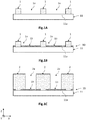
- the Figures 1A to 1K are schematic and partial views, in section, of different steps of a collective manufacturing process of semiconductor structures 20 according to one embodiment.
- the semiconductor structure 20 is a light-emitting diode produced on the basis of InGaN.
- a growth substrate 10 is produced which comprises a support substrate 11 coated at least in part with a nucleation layer 13.
- the support substrate 11 has an upper face 11a intended to receive the nucleation layer 13. It can be made of the same material, and thus be a solid substrate ( bulk substrate, in English), or be formed of a stack of several layers of different materials, such as a SOI type substrate ( Silicon On Insulator, in English).
- the material defining the upper face 11a can be electrically insulating or conductive.
- such an insulating material can be chosen from sapphire (Al 2 O 3 ), borosilicate, silica, glass, quartz, an oxide or a nitride of silicon or aluminum, among others.
- III-V compounds can be III-N compounds, such as GaN, InGaN, AlN, InN or AlInGaN, or compounds comprising an element of column V, for example AsGa or the InP.
- Compounds II-VI can be CdTe, HgTe, CdHgTe, ZnO, ZnMgO, CdZnO or CdZnMgO.
- elements or compounds IV can be Si, C, Ge, SiC, SiGe, GeC, among others.
- the semiconductor material can be doped to increase its electrical conductivity.
- the material of the support substrate 11 defining the upper face 11a can be chosen from metallic materials (Ti, Au, TiAu, etc.) and semi-metallic materials (TiN, etc.).
- the support substrate 11 is here a monobloc substrate made of sapphire.
- a first growth mask 1 is produced on the upper face 11a, intended to subsequently define a free surface of the upper face 11a of the support substrate 11 capable of receiving a working electrode.
- a dielectric layer is deposited on the upper face 11a of the support substrate 11.
- the dielectric layer is made of at least one electrically insulating material, for example a silicon oxide or nitride, such as SiO 2 or Si 3 N 4 , or even a silicon oxynitride, an aluminum oxide, or a hafnium oxide. It may have a dimension along the Z axis, ie a thickness of between a few hundred nanometers and a few microns or tens of microns, for example equal to around 10 ⁇ m.
- the first localized growth mask 1 then forms a mesh of dielectric bands.
- the free surfaces can have, in the XY plane, a circular, oval or polygonal shape, for example square or rectangular. For example, they have a square shape of approximately 100 ⁇ m per side. The dimensions of the free surface depend in particular on those of the semiconductor structures that it is desired to manufacture.
- Each dielectric strip 1 has an initial width, i.e.
- the dielectric strips 1 have an initial thickness equal to approximately 15 ⁇ m and an initial width equal to approximately 15 ⁇ m.
- the initial width of the dielectric strips depends in particular on the dimensions of the working electrode intended to be produced subsequently.
- the nucleation layer 13 is then deposited on the free surfaces of the upper face 11a of the support substrate 11 (fig.iB).
- the nucleation layer 13 can be deposited by epitaxial growth by molecular jets (MBE, for Molecular Beam Epitaxy, in English).
- MBE molecular jets
- Other deposition techniques are possible, for example by chemical vapor deposition (CVD, for Chemical Vapor Deposition, in English) such as chemical deposition with organometallic precursors (MOCVD), or any other suitable deposit technique.
- the nucleation layer 13 is made of tungsten sulfide WS 2 which is particularly suitable for the nucleation of a semiconductor compound based on InGaN.
- the nucleation layer 13 preferably has a number of monolayers chosen such that the separation of the semiconductor structures 20 from the support substrate 11 by electrochemical ablation is carried out before they oxidize, if necessary applicable.
- the semiconductor structures 20 are then produced by van der Waals epitaxy. These are made so as to define a lateral zone 3 which surrounds the semiconductor structures 20 in which are intended to be located a free surface 14 of the nucleation layer 13 and a conductive surface 31 of a working electrode 30.
- the growth mask 2 here has a final thickness greater than the initial thickness of the growth mask 1, the value of the final thickness being a function of the desired dimensions of the semiconductor structures 20.
- a second dielectric layer is deposited so as to completely cover the nucleation layer 13 and the first growth mask 1.
- the second dielectric layer is preferably made of a material identical to that of the first growth mask, and has a thickness substantially equal to the desired final value.
- each dielectric strip 2 has the final thickness and a width final greater than the initial width of the growth mask 1.
- each dielectric strip 2 of the growth mask covers laterally, that is to say transversely to its longitudinal extent, part of the nucleation layer 13 . This part covered is intended to form the free surface 14 of the nucleation layer 13.
- the dielectric strips 2 are intended to subsequently form the lateral zone 3 in which the free surface 14 of the nucleation layer 13 and the conductive surface will be located 31 of the working electrode 30.
- the section of the through openings 2a in the XY plane can have different shapes, for example circular, oval, polygonal, for example square or rectangular.
- the through openings 2a can have lateral dimensions, in the XY plane, of between a few hundred nanometers and a few millimeters, depending on the intended applications.
- the nucleation surface has a square shape with a side of 50 ⁇ m, and the dielectric strips 2 have a final width of approximately 65 ⁇ m.
- the semiconductor structures 20 are then produced in the through openings 2a of the growth mask 2, by epitaxial growth of the van der Waals type from the nucleation surfaces (FIG. ID).
- the semiconductor structures 20 are stacks of semiconductor layers produced on the basis of InGaN and forming a pn junction, intended to form light-emitting diodes.
- the epitaxial growth of the semiconductor structures 20 can be carried out by conventional epitaxy techniques, such as CVD deposition, for example MOCVD, MBE epitaxy, HVPE epitaxy, atomic layer epitaxy (ALE, for Atomic Layer). Epitaxy ) , atomic layer deposition (ALD, for Atomic Layer Deposition ) , or even by evaporation or sputtering .
- CVD deposition for example MOCVD, MBE epitaxy, HVPE epitaxy, atomic layer epitaxy (ALE, for Atomic Layer).
- ALE atomic layer epitaxy
- Epitaxy atomic layer deposition
- ALD atomic layer deposition
- the semiconductor structures 20 are produced based on InGaN by chemical deposition MOCVD.
- each semiconductor structure 20 here comprises, from the nucleation surface, a portion of intrinsic InGaN 21 (not intentionally doped), a first portion 22 doped according to a first type of conductivity, for example of type n, an active area 23 formed of several quantum wells each inserted between two barrier layers, and a second portion 24 doped according to a second type of conductivity opposite to the first type, for example of p type.
- the conductivity types can be reversed.
- Other layers may be provided, for example an electron blocking layer located between the active area and the p-doped portion, and an overdoped portion p intended to facilitate the injection of charge carriers from an electrical contact.
- the semiconductor structures 20 are here produced collectively, that is to say simultaneously, so that the doped portions 22, 24 and the active area 23 of each semiconductor structure 20 advantageously have substantially the same characteristics in terms of dimensions, composition, and doping level.
- the portion 21 of intrinsic InGaN being produced by van der Waals epitaxy from the two-dimensional material of the nucleation layer 13, it has a crystal lattice which is not mechanically constrained by that of the nucleation layer 13, nor by that of the support substrate 11.
- the effective lattice parameter of the material of the portion 21 of intrinsic InGaN is substantially equal to its value in the natural state (unconstrained). This results in a good relaxation of the mechanical stresses of the material of the intrinsic InGaN portion along its entire thickness, thus leading to a low density of structural defects such as dislocations of mesh detuning resulting from a possible plastic relaxation of the stresses. .
- the base material of the semiconductor structure 20 is a ternary or quaternary compound based on GaN, such as InGaN
- a high atomic proportion of aluminum makes it possible to absorb light radiation in the ultraviolet (spectral band between 100nm and 400nm).
- the electrical contacts 25, 26 allowing the injection of the charge carriers into the semiconductor structure 20.
- the lateral flanks of the p-doped portion 24, of the active area 23, and a part of the n-doped portion 22 are etched so as to form a recess receiving a first electrical contact 26.
- lateral flank is meant a surface which laterally delimits, in the XY plane, an element, this surface being able to be oriented in a substantially parallel to the axis Z.
- a second electrical contact 25, for example made of a material transparent to the light radiation emitting from the diode, is deposited on the upper face of the p-doped portion 24.
- the semiconductor structure 20 has an aspect ratio which does not necessarily correspond to the actual aspect ratio.
- the growth mask 2 is not shown.
- the semiconductor structure 20 can have a thickness of the order of a few microns to tens or hundreds of microns, while its lateral dimensions can range up to a few millimeters.
- the growth mask 2 is then removed (fig.iF).
- a plurality of semiconductor structures 20 are obtained which are distinct from each other. They are bordered, i.e. surrounded, by a lateral zone 3 which extends between the lateral flanks facing two adjacent semiconductor structures 20.
- the semiconductor structures 20 cover only part of the nucleation layers 13, so that the latter have a free surface 14 in each lateral zone 3.
- the upper face 11a of the support substrate 11 has a free surface 12 located between two adjacent nucleation layers 13. This free surface 12 is intended to receive a working electrode 30.
- the free surface 14 of each nucleation layer 13 has an upper face 14a opposite the support substrate 11, and a lateral border 14b which defines the periphery of the nucleation layer 13 .
- the working electrode 30 resting on the support substrate 11 is then produced (fig.iG). This is located in the lateral zone 3, and arranged so as to leave free, partially or totally, the free surface 14 of the nucleation layer 13.
- the working electrode 30 thus comprises a conductive surface 31, distinct from the nucleation layer 13 and semiconductor structures 20.
- the working electrode 30 is made of an electrically conductive material.
- the material can be a metal, for example chosen from Au, Pt, TiAu, TiN etc. It can also be the two-dimensional material of the nucleation layer 13 when it is electrically conductive, or even the material of the support substrate 11 defining the upper face 11a when it is electrically conductive.
- the working electrode 30 forms a mesh of conductive strips (FIG. 1H) deposited in contact with the upper face 11a of the support substrate 11 and here at a distance from the nucleation layer 13.
- the thickness and width dimensions of the conductive strips can be between a few hundred nanometers and a few microns.
- the working electrode 30 is electrically connected to a voltage source adapted to impose on it a determined electrical potential.
- the semiconductor structures 20 are bordered, here surrounded, by lateral zones in which are located a conductive surface 31 of the working electrode 30, and a free surface 14 of the nucleation layer 13.
- the free surface 14 is here formed by a part of the upper face 14a and by the lateral flanks 14b (lateral border) of the nucleation layer 13.
- the conductive surface 31 is formed by the upper face and by the lateral flanks of the working electrode 30.
- the structure thus obtained is placed in an aqueous electrolyte bath 50, in which is disposed a second electrode, called reference electrode 40, which has a fixed electrical potential.
- the aqueous electrolyte 50 comes into contact, in the lateral zone 3, of the conductive surface 31 of the working electrode 30, and of the free surface 14 of the nucleation layer 13.
- the aqueous electrolyte 50 is a aqueous solution containing ions. It is chosen so as to have sufficient electrical conductivity. In addition, it is chosen so as to be inert with respect to the material or materials of the semiconductor structures 20, so as not to induce structural degradation.
- the aqueous electrolyte 50 may be acidic and have a pH, for example, of about 2. It can be LiCl 1M with a conductivity equal to 70mS.cm.
- a counter electrode, for example. in platinum can be used (assembly with three electrodes), and the reference electrode 40 can be made of Ag / AgCl or calomel (or any other reference electrode compatible with the electrolyte).
- the semiconductor structures 20 are then separated from the growth substrate 10.
- a potential difference is applied between the working electrode 30 and the reference electrode 40.
- the potential can be applied in continuous mode or in pulsed mode.
- the potential has a value sufficient to generate hydroxyl radicals HO • in the aqueous electrolyte 50, at the interface with the conductive surface 31 of the working electrode 30. This value varies depending on the nature of the electrode and the composition and pH of the electrolyte.
- the hydroxyl radicals correspond to the free radicals HO •, that is to say to the neutral form of the hydroxide ions OH - .
- This formation of hydroxyl radicals can be accompanied by oxidation of the conductive surface 31, as indicated in the article of Avasarala et al. entitled Electrochemical oxidation behavior of titanium nitride based electrocatalysts under PEM fuel cell conditions, Electrochimica Acta, 55 (2010) 9024-9034 , in the case of a TiN electrode under oxidizing conditions at a DC voltage of the order of 1.0V to 1.5V.
- the generation of hydroxyl radicals can be accompanied by the formation of nitrogen N 2 gas capable of inducing a localized separation of the nucleation layer 13, which can then improve the separation of the semiconductor structures 20 from the growth substrate 10.
- the separation is carried out by partial or total degradation of at least one intermediate monolayer 13.2 of the two-dimensional material of the nucleation layer 13, to from the free surface 14, and here from at least its lateral border 14b, by an electrochemical ablation phenomenon similar to that described in the article by Das et al. entitled A Self-Limiting Electro-Ablation Technique for the Top-Down Synthesis of Large-Area Monolayer Flakes of 2D Materials, Sci. Rep. 6, 28195 (2016 ).
- the minimum value of the electric potential imposed on the working electrode 30 to cause the generation of hydroxyl radicals can be predetermined by a method of differential pulse voltammetry (DPV for Differential Pulse Voltammetry, in English).
- the hydroxyl radicals As the fig.1J , due to the strong oxidizing power of the hydroxyl radicals, the latter directly attack the chemical bonds of the two-dimensional material (on the edge of the monolayers) from the free surface 14 of the nucleation layer 13, and here from its lateral edge 14b .
- the hydroxyl radicals are adsorbed by the monolayers of the two-dimensional material, here at from the lateral flank and from the free upper face of the nucleation layer 13, in particular via structural surface defects such as dislocations.
- the adsorption of hydroxyl radicals causes progressive degradation of the interlayer monolayer (s) 13.2, by the formation of a plurality of sheets dissociating from the nucleation layer 13.
- the sheets coming from the intermediate monolayers 13.2 dissociate from the nucleation layer 13 all the more easily as their bonding energy with the other monolayers is lower than that connecting the lower monolayer 13.1 to the support substrate 11, and that connecting the upper monolayer 13.3 to the semiconductor structure 20.
- the binding energy between a lower MOS 2 monolayer and a TiN surface in absolute value, is around 1.25eV, while it is around 0.16eV between monolayers spacers of this two-dimensional MoS 2 material.
- the separation of the semiconductor structures 20 is thus obtained with respect to the support substrate 11.
- the semiconductor structures 20 can then be retrieved in order to finalize the manufacture of a functional optoelectronic system.
- the manufacturing process makes it possible to produce one or more semiconductor structures 20 by van der Waals epitaxy and to separate them from their growth substrate 10.
- the separation step takes advantage of an electrochemical ablation reaction of the nucleation layer 13 in two-dimensional material.
- the semiconductor structures 20 do not undergo mechanical action as in the example of the prior art mentioned above, which makes it possible to preserve their optical and / or electronic properties.
- the upper face 11a of the support substrate 11 can be defined by an electrically conductive material.
- the free surface 12 of the support substrate 11, located in the lateral zone 3, can therefore form the conductive surface 31 of the working electrode 30.
- the latter can thus be the conductive material of the support substrate 11, electrically connected to the voltage source.
- the conductive surface 31 can be defined by the free surface 14 of the nucleation layer 13, in the case where the two-dimensional material is made of an electrically conductive material, such as for example. graphene.
- the nucleation layer 13, in the lateral zone 3, can be distinct from the adjacent nucleation layer 13, but as a variant, the different nucleation layers can form the same continuous nucleation layer 13.
- the various semiconductor structures 20 can, before the separation step, be assembled together to the same secondary substrate (not shown), making it possible in particular to subsequently carry out the steps of structuring and forming the electrical contacts.
- the assembly obtained, formed of the growth substrate 10, the semiconductor structures 20 and the secondary substrate is placed in the aqueous electrolyte 50 and the separation step is carried out as described above.
- a plurality of semiconductor structures 20 are thus obtained, separated from the growth substrate 10, and assembled with the secondary substrate.
- the working electrode 30 is formed of a plurality of conductive strips distinct from each other.
- the polarization of one or more conductive strips adjacent to the identified semiconductor structure 20 makes it possible to separate said semiconductor structure 20 selectively.
- the sum of the voltages applied to the conductive strips adjacent to the chosen semiconductor structure makes it possible to reach the potential necessary for the initiation of the electrochemical ablation reaction (therefore in the vicinity of the chosen structure).
Abstract
L'invention porte sur un procédé de fabrication d'au moins une structure semiconductrice (20) séparée d'un substrat support (11), comportant les étapes suivantes :- réalisation d'une couche de nucléation (13) bidimensionnelle à partir du substrat support (11) ;- réalisation de la structure semiconductrice (20) par épitaxie à partir de la couche de nucléation ;- obtention d'une première électrode (30) située dans une zone latérale (3) qui borde la structure semiconductrice ;- disposition de la structure ainsi obtenue dans un bain d'électrolyte aqueux (50) ;- application d'une différence de potentiel entre les électrodes (30, 40), jusqu'à provoquer la séparation de la structure semiconductrice (20) vis-à-vis du substrat support (11).The invention relates to a method for manufacturing at least one semiconductor structure (20) separate from a support substrate (11), comprising the following steps: - producing a two-dimensional nucleation layer (13) from the substrate support (11); - production of the semiconductor structure (20) by epitaxy from the nucleation layer; - production of a first electrode (30) located in a lateral zone (3) which borders the semiconductor structure; - arrangement of the structure thus obtained in an aqueous electrolyte bath (50); - application of a potential difference between the electrodes (30, 40), until the separation of the semiconductor structure (20) from support substrate screw (11).
Description
Le domaine de l'invention porte sur la fabrication d'au moins une structure semiconductrice par épitaxie de type van der Waals, comportant une étape de séparation de la ou des structures semiconductrices épitaxiées vis-à-vis du substrat de croissance.The field of the invention relates to the manufacture of at least one semiconductor structure by van der Waals type epitaxy, comprising a step of separation of the epitaxial semiconductor structure (s) from the growth substrate.
D'une manière générale, l'épitaxie d'un matériau cristallin à partir d'une couche de nucléation d'un substrat de croissance correspond à la croissance de ce matériau de sorte que son réseau cristallin présente une relation d'épitaxie avec celui du matériau sous-jacent. Autrement dit, le matériau épitaxié présente un alignement des orientations cristallographiques de son réseau cristallin, dans au moins une direction comprise dans le plan du matériau, et dans au moins une direction orthogonale au plan du matériau, avec celles du réseau cristallin du matériau de nucléation. Le plan du matériau épitaxié est ici parallèle au plan de nucléation. Cela se traduit par le fait qu'il y a un accord d'orientation et de position cristallographique entre le réseau cristallin du matériau épitaxié et celui du matériau de nucléation.In general, the epitaxy of a crystalline material from a nucleation layer of a growth substrate corresponds to the growth of this material so that its crystal lattice has an epitaxy relationship with that of underlying material. In other words, the epitaxial material has an alignment of the crystallographic orientations of its crystal lattice, in at least one direction included in the plane of the material, and in at least one direction orthogonal to the plane of the material, with those of the crystal lattice of the nucleating material . The plane of the epitaxial material is here parallel to the nucleation plane. This results in the fact that there is an agreement of orientation and crystallographic position between the crystal lattice of the epitaxial material and that of the nucleating material.
Cependant, lorsque le matériau cristallin présente un paramètre de maille différent de celui du matériau de nucléation, le matériau épitaxié présente alors une déformation de son réseau cristallin, de sorte qu'il subit alors des contraintes mécaniques en tension ou en compression. Par ailleurs, lorsque l'épaisseur du matériau épitaxié dépasse une valeur dite épaisseur critique, les contraintes mécaniques peuvent relaxer de manière plastique, se traduisant alors par la formation de défauts structuraux tels que des dislocations de désaccord de maille. La qualité cristalline de la couche épitaxiée peut alors être dégradée.However, when the crystalline material has a different lattice parameter from that of the nucleation material, the epitaxial material then has a deformation of its crystal lattice, so that it then undergoes mechanical stresses in tension or in compression. Furthermore, when the thickness of the epitaxial material exceeds a value known as the critical thickness, the mechanical stresses can relax in a plastic manner, resulting then in the formation of structural defects such as dislocations of mesh detuning. The crystalline quality of the epitaxial layer can then be degraded.
A titre d'exemple, la croissance épitaxiale d'une couche cristalline en un composé III-N, par exemple du nitrure de gallium GaN ou du nitrure d'indium et de gallium InGaN, peut être effectuée, entre autres, à partir d'un substrat en saphir (Al2O3) ou en silicium. Cependant, le GaN présente un désaccord de maille de l'ordre de 15% avec le saphir, ainsi qu'une importante différence du coefficient de dilatation thermique. Le GaN épitaxié présente alors des contraintes mécaniques qui, à partir d'une épaisseur critique de la couche, peuvent relaxer de manière plastique en formant des dislocations. De tels défauts structuraux sont susceptibles de dégrader les propriétés optiques et/ou électroniques d'un dispositif microélectronique ou optoélectronique comportant une telle couche épitaxiée.By way of example, the epitaxial growth of a crystalline layer into a III-N compound, for example gallium nitride GaN or indium nitride and gallium InGaN, can be made, among other things, from a sapphire (Al 2 O 3 ) or silicon substrate. However, GaN has a mesh mismatch of around 15% with sapphire, as well as a significant difference in the coefficient of thermal expansion. The epitaxial GaN then presents mechanical stresses which, starting from a critical thickness of the layer, can relax in a plastic way by forming dislocations. Such structural defects are liable to degrade the optical and / or electronic properties of a microelectronic or optoelectronic device comprising such an epitaxial layer.
Dans le but de diminuer la densité des défauts structuraux, l'article de
La diode électroluminescente obtenue est ensuite séparée de son substrat de croissance par une étape de séparation mécanique. Plus précisément, une couche de mise en contrainte réalisée en nickel est déposée sur la surface supérieure de la diode électroluminescente, ainsi qu'une couche de manipulation. La couche de nickel impose alors des contraintes mécaniques dans la diode électroluminescente qui provoquent la séparation mécanique de cette dernière vis-à-vis du substrat de croissance. La séparation est dite mécanique dans la mesure où elle est obtenue par la génération de contraintes mécaniques dans la diode électroluminescente telles que leur énergie est supérieure à l'énergie des liaisons van der Waals entre la diode électroluminescente et le substrat de croissance. Cependant, les contraintes mécaniques générées dans la diode électroluminescente par une couche de mise en contrainte sont susceptibles d'induire une dégradation des propriétés optiques et/ou électroniques de la diode électroluminescente.The light-emitting diode obtained is then separated from its growth substrate by a mechanical separation step. More specifically, a stress layer made of nickel is deposited on the upper surface of the light-emitting diode, as well as a handling layer. The nickel layer then imposes mechanical stresses in the light-emitting diode which cause the mechanical separation of the latter from the growth substrate. The separation is said to be mechanical insofar as it is obtained by the generation of mechanical stresses in the light-emitting diode such that their energy is greater than the energy of the van der Waals bonds between the light-emitting diode and the growth substrate. However, the mechanical stresses generated in the light-emitting diode by a stressing layer are capable of inducing a degradation of the optical and / or electronic properties of the light-emitting diode.
L'invention a pour objectif de remédier au moins en partie aux inconvénients de l'art antérieur, et plus particulièrement de proposer un procédé de fabrication d'au moins une structure semiconductrice par épitaxie de type van der Waals, comportant une étape de séparation de la structure semiconductrice vis-à-vis de son substrat de croissance, de sorte que les propriétés optiques et/ou électroniques de la structure semiconductrice soient sensiblement préservées à la suite de l'étape de séparation.The invention aims to remedy at least in part the drawbacks of the prior art, and more particularly to propose a manufacturing process at least one semiconductor structure by van der Waals type epitaxy, comprising a step of separating the semiconductor structure from its growth substrate, so that the optical and / or electronic properties of the semiconductor structure are substantially preserved following the separation step.
Plus précisément, l'objet de l'invention est un procédé de fabrication d'au moins une structure semiconductrice séparée d'un substrat support, comportant les étapes suivantes :
- i) réalisation, à partir d'un substrat support, d'une couche de nucléation formée d'un matériau bidimensionnel comportant au moins trois monocouches ;
- ii) réalisation, par épitaxie à partir de la couche de nucléation, d'au moins une structure semiconductrice, de manière à être bordée par une zone latérale dans laquelle la couche de nucléation présente une surface libre ;
- iii) obtention d'une surface conductrice d'une première électrode, située dans ladite zone latérale et distincte de ladite surface libre ;
- iv) disposition de la structure ainsi obtenue dans un bain d'électrolyte aqueux, dans lequel est disposée une deuxième électrode, l'électrolyte aqueux venant alors au contact, dans la zone latérale, de la surface libre de la couche de nucléation et de la surface conductrice de la première électrode ;
- v) application d'une différence de potentiel entre lesdites électrodes, adaptée à provoquer la formation de radicaux hydroxyles à l'interface entre la surface conductrice et l'électrolyte aqueux, lesquels réagissent alors avec la surface libre de la couche de nucléation jusqu'à provoquer la séparation de la structure semiconductrice vis-à-vis du substrat support.
- i) production, from a support substrate, of a nucleation layer formed of a two-dimensional material comprising at least three monolayers;
- ii) producing, by epitaxy from the nucleation layer, at least one semiconductor structure, so as to be bordered by a lateral zone in which the nucleation layer has a free surface;
- iii) obtaining a conductive surface of a first electrode, located in said lateral zone and distinct from said free surface;
- iv) arrangement of the structure thus obtained in an aqueous electrolyte bath, in which a second electrode is arranged, the aqueous electrolyte then coming into contact, in the lateral zone, with the free surface of the nucleation layer and the conductive surface of the first electrode;
- v) application of a potential difference between said electrodes, adapted to cause the formation of hydroxyl radicals at the interface between the conductive surface and the aqueous electrolyte, which then react with the free surface of the nucleation layer up to cause separation of the semiconductor structure from the support substrate.
Le matériau bidimensionnel est formé d'un empilement d'au moins trois monocouches, dont au moins une monocouche intercalaire. Chaque monocouche, ou feuillet, est formée d'un réseau cristallin bidimensionnel. Par ailleurs, une face supérieure du substrat support, sur laquelle repose la couche de nucléation, comporte une première surface non recouverte par la couche de nucléation. Aussi, la surface libre de la couche de nucléation présente une face supérieure (parallèle à la face supérieure du substrat support) et une bordure latérale.The two-dimensional material is formed from a stack of at least three monolayers, at least one of which is an intermediate monolayer. Each monolayer, or sheet, is formed of a two-dimensional crystal lattice. Furthermore, an upper face of the support substrate, on which the nucleation layer rests, has a first surface not covered by the nucleation layer. Also, the free surface of the nucleation layer has an upper face (parallel to the upper face of the support substrate) and a lateral border.
Certains aspects préférés mais non limitatifs de ce procédé sont les suivants.Some preferred but non-limiting aspects of this process are as follows.
De préférence, à la suite de l'étape i) de réalisation de la couche de nucléation, une face supérieure du substrat support, sur laquelle repose la couche de nucléation, comporte une première surface non recouverte par la couche de nucléation.Preferably, following step i) of producing the nucleation layer, an upper face of the support substrate, on which the nucleation layer rests, has a first surface not covered by the nucleation layer.
De préférence, l'étape iii) d'obtention de la surface conductrice comporte la réalisation d'une portion métallique formant la première électrode, située dans la zone latérale et au contact de la première surface du substrat support.Preferably, step iii) of obtaining the conductive surface comprises the production of a metal portion forming the first electrode, located in the lateral zone and in contact with the first surface of the support substrate.
La surface conductrice de la première électrode peut être située à distance de la surface libre de la couche de nucléation.The conductive surface of the first electrode may be located at a distance from the free surface of the nucleation layer.
La première surface peut être définie par un matériau électriquement conducteur du substrat support lequel forme la première électrode, la première surface formant alors la surface conductrice.The first surface can be defined by an electrically conductive material of the support substrate which forms the first electrode, the first surface then forming the conductive surface.
Le matériau bidimensionnel peut être électriquement conducteur et la couche de nucléation peut former la première électrode, la surface libre de la couche de nucléation formant alors la surface conductrice.The two-dimensional material can be electrically conductive and the nucleation layer can form the first electrode, the free surface of the nucleation layer then forming the conductive surface.
Lors de l'étape ii) de réalisation de la structure semiconductrice, celle-ci peut recouvrir partiellement la couche de nucléation, de sorte que la surface libre de la couche de nucléation est formée au moins en partie par une partie de sa face dite supérieure opposée au substrat support.During step ii) of producing the semiconductor structure, the latter can partially cover the nucleation layer, so that the free surface of the nucleation layer is formed at least in part by part of its so-called upper face opposite the support substrate.
Le matériau bidimensionnel de la couche de nucléation peut être choisi parmi les chalcogénures de métaux de transition, le graphène, et le nitrure de bore.The two-dimensional material of the nucleation layer can be chosen from transition metal chalcogenides, graphene, and boron nitride.
La structure semiconductrice peut être une diode adaptée à émettre ou à détecter de la lumière, et peut être réalisée à base d'un composé semiconducteur III-V ou à base d'un composé semiconducteur II-VI.The semiconductor structure can be a diode adapted to emit or detect light, and can be produced based on a III-V semiconductor compound or based on a II-VI semiconductor compound.
Lors de l'étape ii), une pluralité de structures semiconductrices peuvent être réalisées à partir de couches de nucléation formées en le matériau bidimensionnel et distinctes les unes des autres, chaque structure semiconductrice étant bordée par une zone latérale dans laquelle est située : une surface conductrice, et une première surface de la face supérieure du substrat support, la première surface étant non recouverte par la couche de nucléation.During step ii), a plurality of semiconductor structures can be produced from nucleation layers formed of the two-dimensional material and distinct from each other, each semiconductor structure being bordered by a lateral zone in which is located: a surface conductive, and a first surface of the upper face of the support substrate, the first surface being not covered by the nucleation layer.
Lors de l'étape ii), une pluralité de structures semiconductrices peuvent être réalisées, puis, au moins l'une desdites structures semiconductrices peut être séparée du substrat support de manière sélective, par l'application d'une différence de potentiel entre une première électrode située dans la zone latérale qui borde la structure semiconductrice à séparer, et la deuxième électrode. Par séparation sélective, on entend que la structure semiconductrice est séparée alors que d'autres structures semiconductrices ne le sont pas. Seule la première électrode située dans la zone latérale de la structure semiconductrice à séparer est polarisée. Les premières électrodes situées dans les zones latérales des structures semiconductrices non séparées ne sont alors pas polarisées. Les premières électrodes sont ainsi distinctes et peuvent être polarisées indépendamment les unes des autres.During step ii), a plurality of semiconductor structures can be produced, then at least one of said semiconductor structures can be separated from the support substrate selectively, by applying a potential difference between a first electrode situated in the lateral zone which borders the semiconductor structure to be separated, and the second electrode. By selective separation is meant that the semiconductor structure is separated while other semiconductor structures are not. Only the first electrode located in the lateral zone of the semiconductor structure to be separated is polarized. The first electrodes located in the lateral zones of the non-separated semiconductor structures are then not polarized. The first electrodes are thus distinct and can be polarized independently of each other.
D'autres aspects, buts, avantages et caractéristiques de l'invention apparaîtront mieux à la lecture de la description détaillée suivante de formes de réalisation préférées de celle-ci, donnée à titre d'exemple non limitatif, et faite en référence aux dessins annexés sur lesquels :
- les
figures 1A à 1K illustrent différentes étapes d'un procédé de fabrication collective de plusieurs structures semiconductrices, selon un mode de réalisation, comportant une étape de séparation de celles-ci vis-à-vis du substrat de croissance ; - la
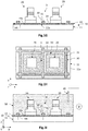
figure 2 est une vue schématique et partielle, en coupe transversale, d'une variante de la fig.iG, dans laquelle la surface conductrice d'une électrode de travail est formée par le substrat support.
- the
Figures 1A to 1K illustrate different steps of a process for the collective production of several semiconductor structures, according to one embodiment, comprising a step of separating them from the growth substrate; - the
figure 2 is a schematic and partial view, in cross section, of a variant of FIG. iG, in which the conductive surface of a working electrode is formed by the support substrate.
Sur les figures et dans la suite de la description, les mêmes références représentent les éléments identiques ou similaires. De plus, les différents éléments ne sont pas représentés à l'échelle de manière à privilégier la clarté des figures. Par ailleurs, les différents modes de réalisation et variantes ne sont pas exclusifs les uns des autres et peuvent être combinés entre eux. Sauf indication contraire, les termes « sensiblement », « environ », « de l'ordre de » signifient à 10% près. Par ailleurs, l'expression « comportant un » doit être comprise comme « comportant au moins un », sauf indication contraire.In the figures and in the following description, the same references represent the same or similar elements. In addition, the different elements are not shown to scale so as to favor the clarity of the figures. Furthermore, the different embodiments and variants are not mutually exclusive and can be combined with one another. Unless otherwise indicated, the terms "substantially", "approximately", "of the order of" mean to within 10%. Furthermore, the expression "comprising a" should be understood as "comprising at least one", unless otherwise indicated.
L'invention porte sur un procédé de fabrication d'au moins une structure semiconductrice par épitaxie de type van der Waals, à partir d'un substrat de croissance comportant une couche de nucléation en un matériau bidimensionnel. Le procédé comprend une étape de séparation de la ou des structures semiconductrices vis-à-vis du substrat de croissance, et en particulier d'un substrat support de ce dernier. Comme décrit en détail plus loin, l'étape de séparation met en oeuvre un phénomène d'ablation électrochimique de la couche de nucléation.The invention relates to a method for manufacturing at least one semiconductor structure by van der Waals type epitaxy, from a growth substrate comprising a nucleation layer of a two-dimensional material. The method comprises a step of separating the semiconductor structure (s) from the growth substrate, and in particular from a support substrate for the latter. As described in detail below, the separation step uses an electrochemical ablation phenomenon of the nucleation layer.
D'une manière générale, l'épitaxie de type van der Waals, également appelée épitaxie van der Waals, est une technique d'hétéroépitaxie par laquelle une couche semiconductrice cristalline est liée à une couche de nucléation formée d'une ou plusieurs monocouches d'un matériau bidimensionnel par des liaisons de type van der Waals et non pas par des liaisons covalentes. L'épitaxie van der Waals permet notamment de s'affranchir du désaccord de maille pouvant exister entre le matériau bidimensionnel et la couche cristalline épitaxiée, ce désaccord de maille étant issu de la différence entre les paramètres de maille des deux matériaux, ce qui permet ainsi d'obtenir une couche cristalline épitaxiée relaxée ou quasi-relaxée. Une telle couche cristalline obtenue par épitaxie van der Waals présente alors une densité réduite de défauts structuraux tels que des dislocations de désaccord de maille, optimisant ainsi les propriétés optiques et/ou électroniques de la structure semiconductrice comportant une telle couche cristalline épitaxiée.In general, van der Waals type epitaxy, also called van der Waals epitaxy, is a heteroepitaxy technique by which a crystalline semiconductor layer is linked to a nucleation layer formed by one or more monolayers of a two-dimensional material by van der Waals type bonds and not by covalent bonds. Van der Waals epitaxy makes it possible in particular to overcome the mesh mismatch that may exist between the two-dimensional material and the epitaxial crystal layer, this mesh mismatch being derived from the difference between the mesh parameters of the two materials, which thus allows to obtain a relaxed or quasi-relaxed epitaxial crystalline layer. Such a crystalline layer obtained by van der Waals epitaxy then exhibits a reduced density of structural defects such as dislocations of mesh mismatch, thereby optimizing the optical and / or electronic properties of the semiconductor structure comprising such an epitaxial crystalline layer.
Le matériau de la couche de nucléation est un matériau cristallin dit bidimensionnel dans la mesure où il est formé d'une monocouche ou de plusieurs monocouches empilées les unes sur les autres, chaque monocouche (également appelée feuille ou feuillet) étant formée d'atomes ou de molécules agencés de manière à former un réseau cristallin bidimensionnel. Autrement dit, le réseau cristallin de chaque monocouche s'étend suivant deux directions et non pas suivant les trois directions de l'espace. Le réseau cristallin d'une monocouche est donc distinct de celui d'une monocouche adjacente. Une monocouche est une structure cristalline bidimensionnelle d'épaisseur monoatomique, et est liée à la ou les monocouches adjacentes par une force de type Van der Waals et non pas par une liaison covalente. Le matériau bidimensionnel peut être choisi parmi les chalcogénures de métaux de transition, tels que le sulfure ou séléniure de molybdène (MoS2, MoSe2) ou de tungstène (WS2), le graphène, le nitrure de bore (en particulier le nitrure de bore hexagonal), entre autres. Dans le cadre de l'invention, le matériau bidimensionnel comporte au moins trois monocouches, c'est-à-dire qu'il est formé d'un empilement d'au moins trois monocouches, à savoir une monocouche dite inférieure au contact d'un substrat support, une monocouche dite supérieure au contact de la ou des structures semiconductrices, et une ou plusieurs monocouches dites intercalaires, situées entre les monocouches inférieure et supérieure. Un tel matériau bidimensionnel est donc différent des composés cristallins dont le réseau cristallin est tridimensionnel.The material of the nucleation layer is a so-called two-dimensional crystalline material insofar as it is formed of a monolayer or of several monolayers stacked on each other, each monolayer (also called sheet or sheet) being formed of atoms or molecules arranged to form a two-dimensional crystal lattice. In other words, the crystal lattice of each monolayer extends in two directions and not in the three directions of space. The crystal lattice of a monolayer is therefore distinct from that of an adjacent monolayer. A monolayer is a two-dimensional crystal structure of monoatomic thickness, and is linked to the adjacent monolayer (s) by a Van der Waals-type force and not by a covalent bond. The two-dimensional material can be chosen from chalcogenides of transition metals, such as molybdenum sulfide or selenide (MoS 2 , MoSe 2 ) or tungsten (WS 2 ), graphene, boron nitride (especially hexagonal boron nitride), among others. In the context of the invention, the two-dimensional material comprises at least three monolayers, that is to say that it is formed of a stack of at least three monolayers, namely a monolayer known as lower than the contact of a support substrate, a so-called upper monolayer in contact with the semiconductor structure or structures, and one or more so-called interlayer monolayers, situated between the lower and upper monolayers. Such a two-dimensional material is therefore different from crystalline compounds whose crystal lattice is three-dimensional.
Comme détaillé plus loin, la séparation de la ou des structures semiconductrices vis-à-vis du substrat de croissance est réalisée par ablation électrochimique de la couche de nucléation. Par ablation électrochimique, on entend une réaction entre une espèce formée de manière électrochimique et pilotée par un potentiel et le matériau bidimensionnel de la couche de nucléation entraînant la suppression partielle ou totale d'au moins une monocouche de la couche de nucléation, en particulier d'au moins une monocouche intercalaire. Cette réaction d'ablation électrochimique se distingue ainsi d'une action d'exfoliation mécanique, dans laquelle on détache ou sépare mécaniquement la structure semiconductrice du substrat de croissance en générant dans cette dernière des contraintes mécaniques, lesquelles sont susceptibles d'induire une dégradation des propriétés optiques et/ou électroniques de la structure semiconductrice.As detailed below, the separation of the semiconductor structure (s) from the growth substrate is carried out by electrochemical ablation of the nucleation layer. By electrochemical ablation is meant a reaction between a species formed electrochemically and driven by a potential and the two-dimensional material of the nucleation layer resulting in the partial or total removal of at least one monolayer from the nucleation layer, in particular d '' at least one intermediate monolayer. This electrochemical ablation reaction is thus distinguished from a mechanical exfoliation action, in which the semiconductor structure is mechanically detached or separated from the growth substrate by generating in the latter mechanical stresses, which are capable of inducing degradation of the optical and / or electronic properties of the semiconductor structure.
Dans la suite de la description, la ou les structures semiconductrices peuvent être des dispositifs microélectroniques ou optoélectroniques. Il peut ainsi s'agir, à titre purement illustratif, de diodes électroluminescentes ou de photodiodes, par exemple réalisées majoritairement à base d'un composé semiconducteur III-V tel que du GaN. Autrement dit, la structure semiconductrice est réalisée en un matériau dont au moins 50% de son volume est formé ou comporte du GaN ou un alliage de GaN, par exemple de l'InGaN ou de l'AlGaN.In the following description, the semiconductor structure or structures can be microelectronic or optoelectronic devices. It can thus be, purely by way of illustration, light-emitting diodes or photodiodes, for example produced mainly based on a III-V semiconductor compound such as GaN. In other words, the semiconductor structure is made of a material of which at least 50% of its volume is formed or comprises GaN or a GaN alloy, for example InGaN or AlGaN.
Les
On définit ici et pour la suite de la description un repère direct tridimensionnel orthogonal (X,Y,Z), où les axes X et Y forment un plan parallèle au plan principal du substrat support 11, et où l'axe Z est orienté de manière sensiblement orthogonale au plan principal du substrat support 11. Dans la suite de la description, les termes « inférieur » et « supérieur » s'entendent comme étant relatifs à un positionnement croissant lorsqu'on s'éloigne du substrat support 11 suivant la direction +Z.We define here and for the rest of the description a direct three-dimensional orthogonal coordinate system (X, Y, Z), where the axes X and Y form a plane parallel to the main plane of the
En référence aux
Le substrat support 11 comporte une face supérieure 11a destinée à recevoir la couche de nucléation 13. Il peut être réalisé en un même matériau, et être ainsi un substrat massif (bulk substrate, en anglais), ou être formé d'un empilement de plusieurs couches de matériaux différents, tel qu'un substrat de type SOI (Silicon On Insulator, en anglais). Le matériau définissant la face supérieure 11a peut être électriquement isolant ou conducteur. A titre d'exemple, un tel matériau isolant peut être choisi parmi le saphir (Al2O3), le borosilicate, la silice, le verre, le quartz, un oxyde ou un nitrure de silicium ou d'aluminium, entre autres.The
Il peut être réalisé en un matériau conducteur tel qu'un semiconducteur éventuellement dopé. A titre d'exemple, un tel matériau semiconducteur peut être choisi parmi le silicium, en germanium, en carbure de silicium, ou plus largement en un composé III-V comportant au moins un élément de la colonne III et au moins un élément de la colonne V du tableau périodique, un composé II-VI, ou en un élément ou un composé IV. A titre d'exemple, des composés III-V peuvent être des composés III-N, tels que le GaN, InGaN, AlN, InN ou l'AlInGaN, ou des composés comportant un élément de la colonne V, par exemple l'AsGa ou l'InP. Des composés II-VI peuvent être le CdTe, HgTe, CdHgTe, ZnO, ZnMgO, CdZnO ou CdZnMgO. Enfin, des éléments ou composés IV peuvent être le Si, C, Ge, SiC, SiGe, GeC, entre autres. Le matériau semiconducteur peut être dopé pour augmenter sa conductivité électrique. Enfin, le matériau du substrat support 11 définissant la face supérieure 11a peut être choisi parmi les matériaux métalliques (Ti, Au, TiAu...) et les matériaux semi-métalliques (TiN...). De préférence, le substrat support 11 est ici un substrat monobloc réalisé en saphir.It can be made of a conductive material such as an optionally doped semiconductor. By way of example, such a semiconductor material can be chosen from silicon, germanium, silicon carbide, or more broadly a III-V compound comprising at least one element from column III and at least one element from the column V of the periodic table, a compound II-VI, or an element or a compound IV. By way of example, III-V compounds can be III-N compounds, such as GaN, InGaN, AlN, InN or AlInGaN, or compounds comprising an element of column V, for example AsGa or the InP. Compounds II-VI can be CdTe, HgTe, CdHgTe, ZnO, ZnMgO, CdZnO or CdZnMgO. Finally, elements or compounds IV can be Si, C, Ge, SiC, SiGe, GeC, among others. The semiconductor material can be doped to increase its electrical conductivity. Finally, the material of the
On réalise ensuite, sur la face supérieure 11a, un premier masque de croissance 1, destiné à définir ultérieurement une surface libre de la face supérieure 11a du substrat support 11 pouvant recevoir une électrode de travail. Pour cela, on dépose une couche diélectrique sur la face supérieure 11a du substrat support 11. La couche diélectrique est réalisée en au moins un matériau électriquement isolant, par exemple un oxyde ou un nitrure de silicium, tel que du SiO2 ou du Si3N4, voire un oxynitrure de silicium, un oxyde d'aluminium, ou un oxyde d'hafnium. Elle peut présenter une dimension suivant l'axe Z, i.e. une épaisseur comprise entre quelques centaines de nanomètres et quelques microns ou dizaines de microns, par exemple égale à 10µm environ.Next, a
On réalise ensuite, par des techniques de photolithographie et de gravure, des ouvertures traversantes 1a dans la couche diélectrique, de manière à rendre localement libre des surfaces de la face supérieure 11a du substrat support 11, destinées à recevoir la couche de nucléation 13. Par surface libre, on entend une surface non revêtue par un autre matériau. Le premier masque de croissance 1 localisée forme alors un maillage de bandes diélectriques. Les surfaces libres peuvent présenter, dans le plan XY, une forme circulaire, ovale ou polygonale, par exemple carrée ou rectangulaire. A titre d'exemple, elles présentent une forme carrée de 100µm environ de côté. Les dimensions de la surface libre dépendent notamment de celles des structures semiconductrices que l'on souhaite fabriquer. Chaque bande diélectrique 1 présente une largeur initiale, i.e. sa dimension transversale dans le plan XY et orthogonale à sa dimension longitudinale, de l'ordre de quelques microns ou dizaines de microns. A titre d'exemple, les bandes diélectriques 1 présentent une épaisseur initiale égale à 15µm environ et une largeur initiale égale à 15µm environ. La largeur initiale des bandes diélectriques dépend notamment des dimensions de l'électrode de travail destinée à être réalisée ultérieurement.Then, by photolithography and etching techniques, through
On dépose ensuite la couche de nucléation 13 sur les surfaces libres de la face supérieure 11a du substrat support 11 (fig.iB). La couche de nucléation 13 peut être déposée par croissance épitaxiale par jets moléculaires (MBE, pour Molecular Beam Epitaxy, en anglais). D'autres techniques de dépôt sont possibles, par exemple par dépôt chimique en phase vapeur (CVD, pour Chemical Vapor Deposition, en anglais) tel que le dépôt chimique aux précurseurs organométalliques (MOCVD), ou tout autre technique de dépôt adaptée. Dans cet exemple, la couche de nucléation 13 est réalisée en sulfure de tungstène WS2 qui est particulièrement adapté à la nucléation d'un composé semiconducteur à base d'InGaN. Elle est formée d'un empilement d'au moins trois monocouches, à savoir une monocouche inférieure au contact de la face supérieure 11a, au moins une monocouche intercalaire, et une monocouche supérieure. La couche de nucléation 13 présente, de préférence, un nombre de monocouches choisi de sorte que la séparation des structures semiconductrices 20 vis-à-vis du substrat support 11 par ablation électrochimique est effectuée avant que celles-ci ne s'oxydent, le cas échéant.The
En référence aux
Pour cela, on réalise ensuite un élargissement du premier masque de croissance 1 de manière à recouvrir partiellement la face supérieure de la couche de nucléation 13 (fig.iC). Cet élargissement est avantageux pour obtenir une surface libre 14 de la couche de nucléation 13 permettant d'optimiser la réaction d'ablation électrochimique lors de l'étape de séparation. De plus, le masque de croissance 2 présente ici une épaisseur finale supérieure à l'épaisseur initiale du masque de croissance 1, la valeur de l'épaisseur finale étant fonction des dimensions souhaitées des structures semiconductrices 20. Aussi, une deuxième couche diélectrique est déposée de manière à recouvrir entièrement la couche de nucléation 13 et le premier masque de croissance 1. La deuxième couche diélectrique est de préférence réalisée en un matériau identique à celui du premier masque de croissance, et présente une épaisseur sensiblement égale à la valeur finale souhaitée.For this, an enlargement of the
On réalise ensuite, par des techniques de photolithographie et de gravure, des ouvertures traversantes 2a dans la deuxième couche diélectrique, de manière à rendre localement libre une surface des couches de nucléation 13. Chaque bande diélectrique 2 présente l'épaisseur finale, et une largeur finale supérieure à la largeur initiale du masque de croissance 1. En d'autres termes, chaque bande diélectrique 2 du masque de croissance recouvre latéralement, c'est-à-dire transversalement à son étendue longitudinale, une partie de la couche de nucléation 13. Cette partie recouverte est destinée à former la surface libre 14 de la couche de nucléation 13. Par ailleurs, les bandes diélectriques 2 sont destinées à former ultérieurement la zone latérale 3 dans laquelle seront situées la surface libre 14 de la couche de nucléation 13 et la surface conductrice 31 de l'électrode de travail 30.Then, by photolithography and etching techniques, through
La section des ouvertures traversantes 2a dans le plan XY peut présenter différentes formes, par exemple circulaire, ovale, polygonale, par exemple carrée ou rectangulaire. Les ouvertures traversantes 2a peuvent présenter des dimensions latérales, dans le plan XY, comprises entre quelques centaines de nanomètres et quelques millimètres, selon les applications visées. Dans cet exemple, la surface de nucléation présente une forme carrée de 50µm de côté, et les bandes diélectriques 2 présentent une largeur finale de 65µm environ.The section of the through
On réalise ensuite les structures semiconductrices 20 dans les ouvertures traversantes 2a du masque de croissance 2, par croissance épitaxiale de type van der Waals à partir des surfaces de nucléation (fig.iD). Dans cet exemple, les structures semiconductrices 20 sont des empilements de couches semiconductrices réalisées à base d'InGaN et formant une jonction pn, destinés à former des diodes électroluminescentes.The
La croissance épitaxiale des structures semiconductrices 20 peut être effectuée par des techniques classiques d'épitaxie, telle que le dépôt CVD, par exemple MOCVD, l'épitaxie MBE, l'épitaxie HVPE, l'épitaxie par couche atomique (ALE, pour Atomic Layer Epitaxy), le dépôt par couche atomique (ALD, pour Atomic Layer Deposition), voire par évaporation ou pulvérisation cathodique (sputtering, en anglais). A titre illustratif, les structures semiconductrices 20 sont réalisées à base d'InGaN par dépôt chimique MOCVD.The epitaxial growth of the
A titre illustratif, chaque structure semiconductrice 20 comporte ici, à partir de la surface de nucléation, une portion d'InGaN intrinsèque 21 (non intentionnellement dopé), une première portion 22 dopée selon un premier type de conductivité, par exemple de type n, une zone active 23 formée de plusieurs puits quantiques intercalés chacun entre deux couches barrières, et une deuxième portion 24 dopée selon un deuxième type de conductivité opposé au premier type, par exemple de type p. Les types de conductivité peuvent être inversés. D'autres couches (non représentées) peuvent être prévues, par exemple une couche de blocage d'électrons située entre la zone active et la portion dopée p, et une portion surdopée p destinée à faciliter l'injection des porteurs de charge à partir d'un contact électrique.By way of illustration, each
Les structures semiconductrices 20 sont ici réalisées de manière collective, c'est-à-dire simultanément, de sorte que les portions dopées 22, 24 et la zone active 23 de chaque structure semiconductrice 20 présentent avantageusement sensiblement les mêmes caractéristiques en termes de dimensions, de composition, et de niveau de dopage.The
La portion 21 d'InGaN intrinsèque étant réalisée par épitaxie van der Waals à partir du matériau bidimensionnel de la couche de nucléation 13, elle présente un réseau cristallin qui n'est pas contraint mécaniquement par celui de la couche de nucléation 13, ni par celui du substrat support 11. Ainsi, le paramètre de maille effectif du matériau de la portion 21 d'InGaN intrinsèque est sensiblement égal à sa valeur à l'état naturel (non contraint). Cela se traduit par une bonne relaxation des contraintes mécaniques du matériau de la portion d'InGaN intrinsèque suivant toute son épaisseur, conduisant ainsi à une faible densité de défauts structuraux tels que les dislocations de désaccord de maille issues d'une éventuelle relaxation plastique des contraintes. Ainsi, il est alors possible de réaliser des portions dopées 22, 23, 24 formant la jonction pn dont l'épaisseur n'est plus limitée par l'épaisseur critique à partir de laquelle une relaxation plastique des contraintes mécaniques apparaît habituellement, améliorant ainsi le rendement quantique interne des structures semiconductrices 20 de type diode électroluminescente ou photodiode. Par ailleurs, dans le cas où le matériau de base de la structure semiconductrice 20 est un composé ternaire ou quaternaire à base de GaN, tel que l'InGaN, il est alors possible d'incorporer une forte quantité d'indium et ainsi obtenir un alliage dont la proportion atomique d'indium est particulièrement élevée, permettant alors d'émettre dans le vert (bande spectrale comprise entre 495nm et 560nm), voire dans le rouge (bande spectrale comprise entre 600nm et 650nm). Dans le cas d'une photodiode à base d'AlGaN, une proportion atomique d'aluminium élevée permet d'absorber un rayonnement lumineux dans l'ultraviolet (bande spectrale comprise entre 100nm et 400nm).The
On peut ensuite réaliser (fig.iE) les contacts électriques 25, 26 permettant l'injection des porteurs de charge dans la structure semiconductrice 20. Dans cet exemple, les flancs latéraux de la portion 24 dopée p, de la zone active 23, et d'une partie de la portion 22 dopée n sont gravées de manière à former un décrochement recevant un premier contact électrique 26. Par flanc latéral, on entend une surface qui délimite latéralement, dans le plan XY, un élément, cette surface pouvant être orientée de manière sensiblement parallèle à l'axe Z. De plus, un deuxième contact électrique 25, par exemple réalisée en un matériau transparent au rayonnement lumineux d'émission de la diode, est déposé sur la face supérieure de la portion 24 dopée p. Sur la
On effectue ensuite le retrait du masque de croissance 2 (fig.iF). Ainsi, on obtient une pluralité de structures semiconductrices 20 distinctes les unes des autres. Elles sont bordées, i.e. entourées, par une zone latérale 3 qui s'étend entre les flancs latéraux se faisant face de deux structures semiconductrices 20 adjacentes. Les structures semiconductrices 20 ne recouvrent qu'une partie des couches de nucléation 13, de sorte que ces dernières présentent une surface libre 14 dans chaque zone latérale 3. De plus, la face supérieure 11a du substrat support 11 présente une surface libre 12 située entre deux couches de nucléation 13 adjacentes. Cette surface libre 12 est destinée à recevoir une électrode de travail 30. La surface libre 14 de chaque couche de nucléation 13 présente une face supérieure 14a opposée au substrat support 11, et une bordure latérale 14b qui définit la périphérie de la couche de nucléation 13.The
En référence aux fig.iG et 1H, on réalise ensuite l'électrode de travail 30 reposant sur le substrat support 11 (fig.iG). Celle-ci est située dans la zone latérale 3, et agencée de manière à laisser libre, partiellement ou totalement, la surface libre 14 de la couche de nucléation 13. L'électrode de travail 30 comporte ainsi une surface conductrice 31, distincte de la couche de nucléation 13 et des structures semiconductrices 20. Dans cet exemple, il n'y a pas contact physique entre l'électrode de travail 30 et les couches de nucléation 13, de sorte que la surface libre 14 n'est pas revêtue par l'électrode de travail 30, ni au niveau de sa face supérieure 14a ni au niveau de sa bordure latérale 14b.With reference to fig.iG and 1H, the working
L'électrode de travail 30 est réalisée en un matériau électriquement conducteur. Le matériau peut être un métal, par exemple choisi parmi Au, Pt, TiAu, TiN etc... Il peut également s'agir du matériau bidimensionnel de la couche de nucléation 13 lorsqu'il est électriquement conducteur, voire le matériau du substrat support 11 définissant la face supérieure 11a lorsqu'il est électriquement conducteur.The working
Dans cet exemple, l'électrode de travail 30 forme un maillage de bandes conductrices (fig.iH) déposées au contact de la face supérieure 11a du substrat support 11 et ici à distance de la couche de nucléation 13. A titre d'exemple, les dimensions en épaisseur et en largeur des bandes conductrices peuvent être comprises entre quelques centaines de nanomètres et quelques microns. L'électrode de travail 30 est électriquement reliée à une source de tension adaptée à lui imposer un potentiel électrique déterminé. Ainsi, les structures semiconductrices 20 sont bordées, ici entourées, par des zones latérales dans lesquelles sont situées une surface conductrice 31 de l'électrode de travail 30, et une surface libre 14 de la couche de nucléation 13. La surface libre 14 est ici formée par une partie de la face supérieure 14a et par les flancs latéraux 14b (bordure latérale) de la couche de nucléation 13. La surface conductrice 31 est formée par la face supérieure et par les flancs latéraux de l'électrode de travail 30.In this example, the working
En référence à la
En référence aux
Comme l'illustre la
De manière similaire au phénomène décrit dans l'article de Das 2016, l'adsorption des radicaux hydroxyles provoque la dégradation progressive de la ou des monocouches intercalaires 13.2, par la formation d'une pluralité de feuillets se dissociant de la couche de nucléation 13. Les feuillets issus des monocouches intercalaires 13.2 se dissocient de la couche de nucléation 13 d'autant plus aisément que leur énergie de liaison avec les autres monocouches est inférieure à celle reliant la monocouche inférieure 13.1 au substrat support 11, et à celle reliant la monocouche supérieure 13.3 à la structure semiconductrice 20. Ainsi, comme l'indique la publication de Das et al. 2016, l'énergie de liaison entre une monocouche inférieure en MOS2 et une surface en TiN, en valeur absolue, est de l'ordre de 1,25eV, alors qu'elle est de l'ordre de 0,16eV entre les monocouches intercalaires de ce matériau bidimensionnel MoS2.Similar to the phenomenon described in the article in Das 2016, the adsorption of hydroxyl radicals causes progressive degradation of the interlayer monolayer (s) 13.2, by the formation of a plurality of sheets dissociating from the
Comme l'illustre la
Ainsi, le procédé de fabrication permet de réaliser une ou plusieurs structures semiconductrices 20 par épitaxie van der Waals et de les séparer de leur substrat de croissance 10. L'étape de séparation met à profit une réaction d'ablation électrochimique de la couche de nucléation 13 en le matériau bidimensionnel. Ainsi, les structures semiconductrices 20 ne subissent pas d'action mécanique comme dans l'exemple de l'art antérieur mentionné précédemment, ce qui permet de préserver leurs propriétés optiques et/ou électroniques.Thus, the manufacturing process makes it possible to produce one or
Des modes de réalisation particuliers viennent d'être décrits. Différentes variantes et modifications apparaîtront à l'homme du métier.Particular embodiments have just been described. Different variants and modifications will appear to those skilled in the art.
Ainsi, comme l'illustre la
Par ailleurs, dans le cas où la face supérieure 11a du substrat support 11 est définie par un matériau électriquement isolant, la surface conductrice 31 peut être définie par la surface libre 14 de la couche de nucléation 13, dans le cas où le matériau bidimensionnel est réalisé en un matériau électriquement conducteur, comme par ex. le graphène. La couche de nucléation 13, dans la zone latérale 3, peut être distincte de la couche de nucléation 13 adjacente, mais en variante, les différentes couches de nucléation peuvent former une même couche de nucléation 13 continue.Furthermore, in the case where the
Par ailleurs, en variante au procédé de fabrication décrit précédemment en référence aux
Par ailleurs, il est possible de procéder à la séparation collective des structures semiconductrices 20, comme décrit précédemment, ou à la séparation sélective de structures semiconductrices 20 préalablement identifiées. Pour cela, l'électrode de travail 30 est formée d'une pluralité de bandes conductrices distinctes les unes des autres. La polarisation d'une ou plusieurs bandes conductrices adjacentes à la structure semiconductrice 20 identifiée permet de séparer ladite structure semiconductrice 20 de manière sélective. Pour cela, la somme des tensions appliquées aux bandes conductrices adjacentes à la structure semiconductrice choisie permet d'atteindre le potentiel nécessaire à l'amorce de la réaction électrochimique d'ablation (donc au voisinage de la structure choisie).Furthermore, it is possible to carry out the collective separation of the
Claims (9)
Applications Claiming Priority (1)
| Application Number | Priority Date | Filing Date | Title |
|---|---|---|---|
| FR1856466A FR3083916B1 (en) | 2018-07-13 | 2018-07-13 | METHOD FOR MANUFACTURING AT LEAST ONE SEMICONDUCTOR STRUCTURE COMPRISING A SEPARATION STEP FROM THE GROWTH SUBSTRATE |
Publications (2)
| Publication Number | Publication Date |
|---|---|
| EP3594997A1 true EP3594997A1 (en) | 2020-01-15 |
| EP3594997B1 EP3594997B1 (en) | 2021-03-24 |
Family
ID=64049351
Family Applications (1)
| Application Number | Title | Priority Date | Filing Date |
|---|---|---|---|
| EP19185598.0A Active EP3594997B1 (en) | 2018-07-13 | 2019-07-10 | Method for manufacturing at least one semiconductor structure comprising a step of separation from the growth substrate |
Country Status (3)
| Country | Link |
|---|---|
| US (1) | US10748762B2 (en) |
| EP (1) | EP3594997B1 (en) |
| FR (1) | FR3083916B1 (en) |
Families Citing this family (1)
| Publication number | Priority date | Publication date | Assignee | Title |
|---|---|---|---|---|
| US20220122837A1 (en) * | 2020-10-21 | 2022-04-21 | University Of South Carolina | Approach for Fabricating N-Polar AlxGa1-xN Devices |
Citations (3)
| Publication number | Priority date | Publication date | Assignee | Title |
|---|---|---|---|---|
| US6956246B1 (en) * | 2004-06-03 | 2005-10-18 | Lumileds Lighting U.S., Llc | Resonant cavity III-nitride light emitting devices fabricated by growth substrate removal |
| US20110223749A1 (en) * | 2009-09-14 | 2011-09-15 | Sumitomo Electric Industries, Ltd. | Method of forming nitride semiconductor epitaxial layer and method of manufacturing nitride semiconductor device |
| EP2770545A2 (en) * | 2013-02-22 | 2014-08-27 | LG Electronics, Inc. | Growth substrate, nitride semiconductor device and method of manufacturing the same |
-
2018
- 2018-07-13 FR FR1856466A patent/FR3083916B1/en not_active Expired - Fee Related
-
2019
- 2019-07-10 EP EP19185598.0A patent/EP3594997B1/en active Active
- 2019-07-11 US US16/508,503 patent/US10748762B2/en active Active
Patent Citations (3)
| Publication number | Priority date | Publication date | Assignee | Title |
|---|---|---|---|---|
| US6956246B1 (en) * | 2004-06-03 | 2005-10-18 | Lumileds Lighting U.S., Llc | Resonant cavity III-nitride light emitting devices fabricated by growth substrate removal |
| US20110223749A1 (en) * | 2009-09-14 | 2011-09-15 | Sumitomo Electric Industries, Ltd. | Method of forming nitride semiconductor epitaxial layer and method of manufacturing nitride semiconductor device |
| EP2770545A2 (en) * | 2013-02-22 | 2014-08-27 | LG Electronics, Inc. | Growth substrate, nitride semiconductor device and method of manufacturing the same |
Non-Patent Citations (5)
| Title |
|---|
| DAS ET AL.: "A Self-Limiting Electro-Ablation Technique for the Top-Down Synthesis of Large-Area Monolayer Flakes of 2D Materials", SCI. REP., vol. 6, 2016, pages 28195 |
| D'AVASARALA ET AL.: "Electrochemical oxidation behavior of titanium nitride based electrocatalysts under PEMfuel cell conditions", ELECTROCHIMICA ACTA, vol. 55, 2010, pages 9024 - 9034 |
| JEEHWAN KIM ET AL: "Principle of direct van der Waals epitaxy of single-crystalline films on epitaxial graphene", NATURE COMMUNICATIONS, vol. 5, 1 September 2014 (2014-09-01), GB, pages 4836 - 4836, XP055468472, ISSN: 2041-1723, DOI: 10.1038/ncomms5836 * |
| KIM ET AL.: "Principle of direct van der Waals epitaxy of single-crystalline films on epitaxial graphene", NAT. COMM., vol. 5, 2014, pages 4836, XP055468472, DOI: doi:10.1038/ncomms5836 |
| SAPTARSHI DAS ET AL: "A Self-Limiting Electro-Ablation Technique for the Top-Down Synthesis of Large-Area Monolayer Flakes of 2D Materials", SCIENTIFIC REPORTS, vol. 6, no. 1, 21 June 2016 (2016-06-21), pages 1, XP055563998, DOI: 10.1038/srep28195 * |
Also Published As
| Publication number | Publication date |
|---|---|
| US10748762B2 (en) | 2020-08-18 |
| FR3083916B1 (en) | 2020-07-17 |
| FR3083916A1 (en) | 2020-01-17 |
| EP3594997B1 (en) | 2021-03-24 |
| US20200020527A1 (en) | 2020-01-16 |
Similar Documents
| Publication | Publication Date | Title |
|---|---|---|
| EP3514841B1 (en) | Optoelectronic device and method for manufacturing same | |
| US20090146142A1 (en) | Light-emitting device including nanorod and method of manufacturing the same | |
| EP2997605B1 (en) | Optoelectronic device and method of manufacturing the same | |
| EP3782193B1 (en) | Method of manufacturing an optoelectronic device having a matrix of diodes | |
| EP3090450B1 (en) | Optoelectronic device comprising semiconductor elements and its fabrication process | |
| WO2013149964A1 (en) | Optoelectronic semiconducting structure with nanowires and method of fabricating such a structure | |
| FR2969995A1 (en) | Producing nitride nanostructures e.g. nanowires on side of substrate, by forming base of nanostructures made of wurtzite nitride phase on substrate, and forming upper part of nanostructures made of nitrides having zinc-blende phase on base | |
| WO2015052456A1 (en) | Hemt made from a heterojunction | |
| EP3241246B1 (en) | Process for fabricating semiconductor nanowires or microwires having insulated base | |
| WO2020260548A1 (en) | Axial-type optoelectronic device with light-emitting diodes and method for manufacturing same | |
| EP3503222A1 (en) | Method for manufacturing an optoelectronic device by transferring a conversion structure onto an emission structure | |
| EP3164881B1 (en) | Optoelectronic device having semiconductor elements and method for manufacturing same | |
| EP3594997B1 (en) | Method for manufacturing at least one semiconductor structure comprising a step of separation from the growth substrate | |
| EP3646391B1 (en) | Optoelectronic device and a method for manufacturing an optoelectronic device | |
| FR3068994A1 (en) | PROCESS FOR MAKING A CRYSTALLINE LAYER IN A III-N COMPOUND BY EPITAXIA VAN DER WAALS FROM GRAPHENE | |
| EP4020604A1 (en) | Method for manufacturing an optoelectronic device comprising group iii nitride-based micro-leds | |
| WO2022069431A1 (en) | Color-display light-emitting-diode optoelectronic device | |
| WO2021009316A1 (en) | Light-emitting diode and method for manufacturing same | |
| WO2014114730A1 (en) | Method for the production of a layer comprising group-iii-element nitride by means of spontaneous delamination | |
| EP3973579B1 (en) | Optoelectronic device with light-emitting diodes a doped region of which incorporates an external segment based on aluminium and gallium nitride | |
| EP2782145A1 (en) | Method for manufacturing a multijunction photovoltaic device and resulting multijunction photovoltaic device | |
| FR3023978A1 (en) | OPTOELECTRONIC DEVICE WITH ELECTROLUMINESCENT DIODE |
Legal Events
| Date | Code | Title | Description |
|---|---|---|---|
| PUAI | Public reference made under article 153(3) epc to a published international application that has entered the european phase |
Free format text: ORIGINAL CODE: 0009012 |
|
| STAA | Information on the status of an ep patent application or granted ep patent |
Free format text: STATUS: REQUEST FOR EXAMINATION WAS MADE |
|
| 17P | Request for examination filed |
Effective date: 20190710 |
|
| AK | Designated contracting states |
Kind code of ref document: A1 Designated state(s): AL AT BE BG CH CY CZ DE DK EE ES FI FR GB GR HR HU IE IS IT LI LT LU LV MC MK MT NL NO PL PT RO RS SE SI SK SM TR |
|
| AX | Request for extension of the european patent |
Extension state: BA ME |
|
| RIC1 | Information provided on ipc code assigned before grant |
Ipc: H01L 33/12 20100101ALN20200903BHEP Ipc: H01L 33/00 20100101ALI20200903BHEP Ipc: H01L 21/78 20060101AFI20200903BHEP |
|
| GRAP | Despatch of communication of intention to grant a patent |
Free format text: ORIGINAL CODE: EPIDOSNIGR1 |
|
| STAA | Information on the status of an ep patent application or granted ep patent |
Free format text: STATUS: GRANT OF PATENT IS INTENDED |
|
| RIC1 | Information provided on ipc code assigned before grant |
Ipc: H01L 33/12 20100101ALN20200929BHEP Ipc: H01L 21/78 20060101AFI20200929BHEP Ipc: H01L 33/00 20100101ALI20200929BHEP |
|
| INTG | Intention to grant announced |
Effective date: 20201030 |
|
| GRAS | Grant fee paid |
Free format text: ORIGINAL CODE: EPIDOSNIGR3 |
|
| GRAA | (expected) grant |
Free format text: ORIGINAL CODE: 0009210 |
|
| STAA | Information on the status of an ep patent application or granted ep patent |
Free format text: STATUS: THE PATENT HAS BEEN GRANTED |
|
| AK | Designated contracting states |
Kind code of ref document: B1 Designated state(s): AL AT BE BG CH CY CZ DE DK EE ES FI FR GB GR HR HU IE IS IT LI LT LU LV MC MK MT NL NO PL PT RO RS SE SI SK SM TR |
|
| REG | Reference to a national code |
Ref country code: GB Ref legal event code: FG4D Free format text: NOT ENGLISH |
|
| REG | Reference to a national code |
Ref country code: CH Ref legal event code: EP |
|
| REG | Reference to a national code |
Ref country code: IE Ref legal event code: FG4D Free format text: LANGUAGE OF EP DOCUMENT: FRENCH |
|
| REG | Reference to a national code |
Ref country code: DE Ref legal event code: R096 Ref document number: 602019003385 Country of ref document: DE Ref country code: AT Ref legal event code: REF Ref document number: 1375352 Country of ref document: AT Kind code of ref document: T Effective date: 20210415 |
|
| REG | Reference to a national code |
Ref country code: LT Ref legal event code: MG9D |
|
| PG25 | Lapsed in a contracting state [announced via postgrant information from national office to epo] |
Ref country code: NO Free format text: LAPSE BECAUSE OF FAILURE TO SUBMIT A TRANSLATION OF THE DESCRIPTION OR TO PAY THE FEE WITHIN THE PRESCRIBED TIME-LIMIT Effective date: 20210624 Ref country code: GR Free format text: LAPSE BECAUSE OF FAILURE TO SUBMIT A TRANSLATION OF THE DESCRIPTION OR TO PAY THE FEE WITHIN THE PRESCRIBED TIME-LIMIT Effective date: 20210625 Ref country code: FI Free format text: LAPSE BECAUSE OF FAILURE TO SUBMIT A TRANSLATION OF THE DESCRIPTION OR TO PAY THE FEE WITHIN THE PRESCRIBED TIME-LIMIT Effective date: 20210324 Ref country code: HR Free format text: LAPSE BECAUSE OF FAILURE TO SUBMIT A TRANSLATION OF THE DESCRIPTION OR TO PAY THE FEE WITHIN THE PRESCRIBED TIME-LIMIT Effective date: 20210324 Ref country code: BG Free format text: LAPSE BECAUSE OF FAILURE TO SUBMIT A TRANSLATION OF THE DESCRIPTION OR TO PAY THE FEE WITHIN THE PRESCRIBED TIME-LIMIT Effective date: 20210624 |
|
| PG25 | Lapsed in a contracting state [announced via postgrant information from national office to epo] |
Ref country code: LV Free format text: LAPSE BECAUSE OF FAILURE TO SUBMIT A TRANSLATION OF THE DESCRIPTION OR TO PAY THE FEE WITHIN THE PRESCRIBED TIME-LIMIT Effective date: 20210324 Ref country code: SE Free format text: LAPSE BECAUSE OF FAILURE TO SUBMIT A TRANSLATION OF THE DESCRIPTION OR TO PAY THE FEE WITHIN THE PRESCRIBED TIME-LIMIT Effective date: 20210324 Ref country code: RS Free format text: LAPSE BECAUSE OF FAILURE TO SUBMIT A TRANSLATION OF THE DESCRIPTION OR TO PAY THE FEE WITHIN THE PRESCRIBED TIME-LIMIT Effective date: 20210324 |
|
| REG | Reference to a national code |
Ref country code: NL Ref legal event code: MP Effective date: 20210324 |
|
| REG | Reference to a national code |
Ref country code: AT Ref legal event code: MK05 Ref document number: 1375352 Country of ref document: AT Kind code of ref document: T Effective date: 20210324 |
|
| PG25 | Lapsed in a contracting state [announced via postgrant information from national office to epo] |
Ref country code: NL Free format text: LAPSE BECAUSE OF FAILURE TO SUBMIT A TRANSLATION OF THE DESCRIPTION OR TO PAY THE FEE WITHIN THE PRESCRIBED TIME-LIMIT Effective date: 20210324 |
|
| PG25 | Lapsed in a contracting state [announced via postgrant information from national office to epo] |
Ref country code: LT Free format text: LAPSE BECAUSE OF FAILURE TO SUBMIT A TRANSLATION OF THE DESCRIPTION OR TO PAY THE FEE WITHIN THE PRESCRIBED TIME-LIMIT Effective date: 20210324 Ref country code: EE Free format text: LAPSE BECAUSE OF FAILURE TO SUBMIT A TRANSLATION OF THE DESCRIPTION OR TO PAY THE FEE WITHIN THE PRESCRIBED TIME-LIMIT Effective date: 20210324 Ref country code: CZ Free format text: LAPSE BECAUSE OF FAILURE TO SUBMIT A TRANSLATION OF THE DESCRIPTION OR TO PAY THE FEE WITHIN THE PRESCRIBED TIME-LIMIT Effective date: 20210324 Ref country code: AT Free format text: LAPSE BECAUSE OF FAILURE TO SUBMIT A TRANSLATION OF THE DESCRIPTION OR TO PAY THE FEE WITHIN THE PRESCRIBED TIME-LIMIT Effective date: 20210324 Ref country code: SM Free format text: LAPSE BECAUSE OF FAILURE TO SUBMIT A TRANSLATION OF THE DESCRIPTION OR TO PAY THE FEE WITHIN THE PRESCRIBED TIME-LIMIT Effective date: 20210324 |
|
| PG25 | Lapsed in a contracting state [announced via postgrant information from national office to epo] |
Ref country code: RO Free format text: LAPSE BECAUSE OF FAILURE TO SUBMIT A TRANSLATION OF THE DESCRIPTION OR TO PAY THE FEE WITHIN THE PRESCRIBED TIME-LIMIT Effective date: 20210324 Ref country code: PT Free format text: LAPSE BECAUSE OF FAILURE TO SUBMIT A TRANSLATION OF THE DESCRIPTION OR TO PAY THE FEE WITHIN THE PRESCRIBED TIME-LIMIT Effective date: 20210726 Ref country code: SK Free format text: LAPSE BECAUSE OF FAILURE TO SUBMIT A TRANSLATION OF THE DESCRIPTION OR TO PAY THE FEE WITHIN THE PRESCRIBED TIME-LIMIT Effective date: 20210324 Ref country code: PL Free format text: LAPSE BECAUSE OF FAILURE TO SUBMIT A TRANSLATION OF THE DESCRIPTION OR TO PAY THE FEE WITHIN THE PRESCRIBED TIME-LIMIT Effective date: 20210324 Ref country code: IS Free format text: LAPSE BECAUSE OF FAILURE TO SUBMIT A TRANSLATION OF THE DESCRIPTION OR TO PAY THE FEE WITHIN THE PRESCRIBED TIME-LIMIT Effective date: 20210724 |
|
| REG | Reference to a national code |
Ref country code: DE Ref legal event code: R097 Ref document number: 602019003385 Country of ref document: DE |
|
| PG25 | Lapsed in a contracting state [announced via postgrant information from national office to epo] |
Ref country code: ES Free format text: LAPSE BECAUSE OF FAILURE TO SUBMIT A TRANSLATION OF THE DESCRIPTION OR TO PAY THE FEE WITHIN THE PRESCRIBED TIME-LIMIT Effective date: 20210324 Ref country code: DK Free format text: LAPSE BECAUSE OF FAILURE TO SUBMIT A TRANSLATION OF THE DESCRIPTION OR TO PAY THE FEE WITHIN THE PRESCRIBED TIME-LIMIT Effective date: 20210324 Ref country code: AL Free format text: LAPSE BECAUSE OF FAILURE TO SUBMIT A TRANSLATION OF THE DESCRIPTION OR TO PAY THE FEE WITHIN THE PRESCRIBED TIME-LIMIT Effective date: 20210324 |
|
| PLBE | No opposition filed within time limit |
Free format text: ORIGINAL CODE: 0009261 |
|
| STAA | Information on the status of an ep patent application or granted ep patent |
Free format text: STATUS: NO OPPOSITION FILED WITHIN TIME LIMIT |
|
| PG25 | Lapsed in a contracting state [announced via postgrant information from national office to epo] |
Ref country code: SI Free format text: LAPSE BECAUSE OF FAILURE TO SUBMIT A TRANSLATION OF THE DESCRIPTION OR TO PAY THE FEE WITHIN THE PRESCRIBED TIME-LIMIT Effective date: 20210324 |
|
| 26N | No opposition filed |
Effective date: 20220104 |
|
| PG25 | Lapsed in a contracting state [announced via postgrant information from national office to epo] |
Ref country code: MC Free format text: LAPSE BECAUSE OF FAILURE TO SUBMIT A TRANSLATION OF THE DESCRIPTION OR TO PAY THE FEE WITHIN THE PRESCRIBED TIME-LIMIT Effective date: 20210324 |
|
| REG | Reference to a national code |
Ref country code: BE Ref legal event code: MM Effective date: 20210731 |
|
| PG25 | Lapsed in a contracting state [announced via postgrant information from national office to epo] |
Ref country code: IS Free format text: LAPSE BECAUSE OF FAILURE TO SUBMIT A TRANSLATION OF THE DESCRIPTION OR TO PAY THE FEE WITHIN THE PRESCRIBED TIME-LIMIT Effective date: 20210724 Ref country code: LU Free format text: LAPSE BECAUSE OF NON-PAYMENT OF DUE FEES Effective date: 20210710 |
|
| PG25 | Lapsed in a contracting state [announced via postgrant information from national office to epo] |
Ref country code: IE Free format text: LAPSE BECAUSE OF NON-PAYMENT OF DUE FEES Effective date: 20210710 Ref country code: BE Free format text: LAPSE BECAUSE OF NON-PAYMENT OF DUE FEES Effective date: 20210731 |
|
| PG25 | Lapsed in a contracting state [announced via postgrant information from national office to epo] |
Ref country code: IT Free format text: LAPSE BECAUSE OF FAILURE TO SUBMIT A TRANSLATION OF THE DESCRIPTION OR TO PAY THE FEE WITHIN THE PRESCRIBED TIME-LIMIT Effective date: 20210324 |
|
| REG | Reference to a national code |
Ref country code: CH Ref legal event code: PL |
|
| PG25 | Lapsed in a contracting state [announced via postgrant information from national office to epo] |
Ref country code: LI Free format text: LAPSE BECAUSE OF NON-PAYMENT OF DUE FEES Effective date: 20220731 Ref country code: CH Free format text: LAPSE BECAUSE OF NON-PAYMENT OF DUE FEES Effective date: 20220731 |
|
| PG25 | Lapsed in a contracting state [announced via postgrant information from national office to epo] |
Ref country code: CY Free format text: LAPSE BECAUSE OF FAILURE TO SUBMIT A TRANSLATION OF THE DESCRIPTION OR TO PAY THE FEE WITHIN THE PRESCRIBED TIME-LIMIT Effective date: 20210324 |
|
| PG25 | Lapsed in a contracting state [announced via postgrant information from national office to epo] |
Ref country code: HU Free format text: LAPSE BECAUSE OF FAILURE TO SUBMIT A TRANSLATION OF THE DESCRIPTION OR TO PAY THE FEE WITHIN THE PRESCRIBED TIME-LIMIT; INVALID AB INITIO Effective date: 20190710 |
|
| PGFP | Annual fee paid to national office [announced via postgrant information from national office to epo] |
Ref country code: GB Payment date: 20230724 Year of fee payment: 5 |
|
| PGFP | Annual fee paid to national office [announced via postgrant information from national office to epo] |
Ref country code: FR Payment date: 20230724 Year of fee payment: 5 Ref country code: DE Payment date: 20230720 Year of fee payment: 5 |