EP3588554A1 - Electronic device, connector, and method for producing electronic device - Google Patents
Electronic device, connector, and method for producing electronic device Download PDFInfo
- Publication number
- EP3588554A1 EP3588554A1 EP17838112.5A EP17838112A EP3588554A1 EP 3588554 A1 EP3588554 A1 EP 3588554A1 EP 17838112 A EP17838112 A EP 17838112A EP 3588554 A1 EP3588554 A1 EP 3588554A1
- Authority
- EP
- European Patent Office
- Prior art keywords
- terminal
- front surface
- electronic device
- head part
- surface side
- Prior art date
- Legal status (The legal status is an assumption and is not a legal conclusion. Google has not performed a legal analysis and makes no representation as to the accuracy of the status listed.)
- Granted
Links
Images



Classifications
-
- H—ELECTRICITY
- H10—SEMICONDUCTOR DEVICES; ELECTRIC SOLID-STATE DEVICES NOT OTHERWISE PROVIDED FOR
- H10W—GENERIC PACKAGES, INTERCONNECTIONS, CONNECTORS OR OTHER CONSTRUCTIONAL DETAILS OF DEVICES COVERED BY CLASS H10
- H10W70/00—Package substrates; Interposers; Redistribution layers [RDL]
- H10W70/40—Leadframes
- H10W70/481—Leadframes for devices being provided for in groups H10D8/00 - H10D48/00
-
- H—ELECTRICITY
- H10—SEMICONDUCTOR DEVICES; ELECTRIC SOLID-STATE DEVICES NOT OTHERWISE PROVIDED FOR
- H10W—GENERIC PACKAGES, INTERCONNECTIONS, CONNECTORS OR OTHER CONSTRUCTIONAL DETAILS OF DEVICES COVERED BY CLASS H10
- H10W20/00—Interconnections in chips, wafers or substrates
- H10W20/40—Interconnections external to wafers or substrates, e.g. back-end-of-line [BEOL] metallisations or vias connecting to gate electrodes
-
- H—ELECTRICITY
- H10—SEMICONDUCTOR DEVICES; ELECTRIC SOLID-STATE DEVICES NOT OTHERWISE PROVIDED FOR
- H10W—GENERIC PACKAGES, INTERCONNECTIONS, CONNECTORS OR OTHER CONSTRUCTIONAL DETAILS OF DEVICES COVERED BY CLASS H10
- H10W70/00—Package substrates; Interposers; Redistribution layers [RDL]
- H10W70/40—Leadframes
- H10W70/411—Chip-supporting parts, e.g. die pads
- H10W70/417—Bonding materials between chips and die pads
-
- H—ELECTRICITY
- H10—SEMICONDUCTOR DEVICES; ELECTRIC SOLID-STATE DEVICES NOT OTHERWISE PROVIDED FOR
- H10W—GENERIC PACKAGES, INTERCONNECTIONS, CONNECTORS OR OTHER CONSTRUCTIONAL DETAILS OF DEVICES COVERED BY CLASS H10
- H10W70/00—Package substrates; Interposers; Redistribution layers [RDL]
- H10W70/40—Leadframes
- H10W70/421—Shapes or dispositions
-
- H—ELECTRICITY
- H10—SEMICONDUCTOR DEVICES; ELECTRIC SOLID-STATE DEVICES NOT OTHERWISE PROVIDED FOR
- H10W—GENERIC PACKAGES, INTERCONNECTIONS, CONNECTORS OR OTHER CONSTRUCTIONAL DETAILS OF DEVICES COVERED BY CLASS H10
- H10W70/00—Package substrates; Interposers; Redistribution layers [RDL]
- H10W70/40—Leadframes
- H10W70/421—Shapes or dispositions
- H10W70/424—Cross-sectional shapes
- H10W70/427—Bent parts
-
- H—ELECTRICITY
- H10—SEMICONDUCTOR DEVICES; ELECTRIC SOLID-STATE DEVICES NOT OTHERWISE PROVIDED FOR
- H10W—GENERIC PACKAGES, INTERCONNECTIONS, CONNECTORS OR OTHER CONSTRUCTIONAL DETAILS OF DEVICES COVERED BY CLASS H10
- H10W70/00—Package substrates; Interposers; Redistribution layers [RDL]
- H10W70/40—Leadframes
- H10W70/464—Additional interconnections in combination with leadframes
- H10W70/466—Tape carriers or flat leads
-
- H—ELECTRICITY
- H10—SEMICONDUCTOR DEVICES; ELECTRIC SOLID-STATE DEVICES NOT OTHERWISE PROVIDED FOR
- H10W—GENERIC PACKAGES, INTERCONNECTIONS, CONNECTORS OR OTHER CONSTRUCTIONAL DETAILS OF DEVICES COVERED BY CLASS H10
- H10W72/00—Interconnections or connectors in packages
-
- H—ELECTRICITY
- H10—SEMICONDUCTOR DEVICES; ELECTRIC SOLID-STATE DEVICES NOT OTHERWISE PROVIDED FOR
- H10W—GENERIC PACKAGES, INTERCONNECTIONS, CONNECTORS OR OTHER CONSTRUCTIONAL DETAILS OF DEVICES COVERED BY CLASS H10
- H10W72/00—Interconnections or connectors in packages
- H10W72/20—Bump connectors, e.g. solder bumps or copper pillars; Dummy bumps; Thermal bumps
-
- H—ELECTRICITY
- H10—SEMICONDUCTOR DEVICES; ELECTRIC SOLID-STATE DEVICES NOT OTHERWISE PROVIDED FOR
- H10W—GENERIC PACKAGES, INTERCONNECTIONS, CONNECTORS OR OTHER CONSTRUCTIONAL DETAILS OF DEVICES COVERED BY CLASS H10
- H10W72/00—Interconnections or connectors in packages
- H10W72/90—Bond pads, in general
-
- H—ELECTRICITY
- H10—SEMICONDUCTOR DEVICES; ELECTRIC SOLID-STATE DEVICES NOT OTHERWISE PROVIDED FOR
- H10W—GENERIC PACKAGES, INTERCONNECTIONS, CONNECTORS OR OTHER CONSTRUCTIONAL DETAILS OF DEVICES COVERED BY CLASS H10
- H10W74/00—Encapsulations, e.g. protective coatings
- H10W74/10—Encapsulations, e.g. protective coatings characterised by their shape or disposition
-
- H—ELECTRICITY
- H10—SEMICONDUCTOR DEVICES; ELECTRIC SOLID-STATE DEVICES NOT OTHERWISE PROVIDED FOR
- H10W—GENERIC PACKAGES, INTERCONNECTIONS, CONNECTORS OR OTHER CONSTRUCTIONAL DETAILS OF DEVICES COVERED BY CLASS H10
- H10W72/00—Interconnections or connectors in packages
- H10W72/90—Bond pads, in general
- H10W72/921—Structures or relative sizes of bond pads
- H10W72/926—Multiple bond pads having different sizes
-
- H—ELECTRICITY
- H10—SEMICONDUCTOR DEVICES; ELECTRIC SOLID-STATE DEVICES NOT OTHERWISE PROVIDED FOR
- H10W—GENERIC PACKAGES, INTERCONNECTIONS, CONNECTORS OR OTHER CONSTRUCTIONAL DETAILS OF DEVICES COVERED BY CLASS H10
- H10W90/00—Package configurations
- H10W90/701—Package configurations characterised by the relative positions of pads or connectors relative to package parts
- H10W90/751—Package configurations characterised by the relative positions of pads or connectors relative to package parts of bond wires
- H10W90/756—Package configurations characterised by the relative positions of pads or connectors relative to package parts of bond wires between a chip and a stacked lead frame, conducting package substrate or heat sink
Definitions
- the present invention relates to an electronic device, a connection body, and a manufacturing method for electronic device.
- a semiconductor element is placed on a conductor layer of a substrate, and a front surface of the semiconductor element and a terminal are connected to each other with a wire or a connector via a conductive adhesive such as solder (refer to JP 2015-12065 A ).
- a conductive adhesive such as solder
- the present invention provides a highly-reliable electronic device in which the thickness of the conductive adhesive is secured while using an appropriate amount of conductive adhesive, and a connection body used in such electronic device.
- An electronic device comprises:
- the first terminal and the second terminal may extend in opposite directions from the head part.
- the electronic element may have a withstand voltage structure
- the electronic device may further comprise:
- the first avoiding part may be a first concave part concaved so as to be separated from the electronic element and the second avoiding part may be a second concave part concaved so as to be separated from the electronic element.
- the first terminal may be a power terminal
- the second terminal may be a sensing terminal
- a back surface side height of the first terminal may correspond to a back surface side height of the second terminal.
- the head part may be integrally formed with the first terminal and the second terminal.
- a connection body used in an electronic device having a sealing part and an electronic element provided inside the sealing part, comprises:
- a manufacturing method for an electronic device comprises; a step of preparing a sealing part, a first terminal for projecting outward from a first side surface of the sealing part, a second terminal for projecting outward from a second side surface different from the first side surface of the sealing part, and a head part coupled to the first terminal and the second terminal and for being connected to a front surface of an electronic element via a conductive adhesive; a step of placing the conductive adhesive on the electronic element; and a step of placing the first terminal and the second terminal on a jig so that the head part is connected to the front surface of the electronic element via the conductive adhesive.
- the first terminal and the second terminal extending in the direction different from that of the first terminal are coupled to the head part, so that the first terminal and the second terminal can be utilized as jig receivers. Therefore, it is possible to prevent the thickness of the conductive adhesive such as solder provided on the front surface of the electronic element from becoming thin due to a weight of the connecting unit by adjusting the heights of the back surface of the first terminal and the back surface of the second terminal by using jig and the like and sealing the same with the sealing resin and the like.
- a semiconductor device being an example of an electronic device of this embodiment may have a sealing part 90 (refer to Fig. 1 ) made of a sealing resin and the like, a first main terminal 11 being a first terminal projecting outward from a first side surface of the sealing part 90, a sensing terminal 13 being a second terminal projecting outward from a second side surface different from the first side surface of the sealing part 90, a semiconductor element 95 provided inside the sealing part 90, and a head part 40 coupled to the first main terminal 11 and the sensing terminal 13 and connected to a front surface of the semiconductor element 95 via a conductive adhesive 75.
- a sealing part 90 made of a sealing resin and the like
- a first main terminal 11 being a first terminal projecting outward from a first side surface of the sealing part 90
- a sensing terminal 13 being a second terminal projecting outward from a second side surface different from the first side surface of the sealing part 90
- a semiconductor element 95 provided inside the sealing part 90
- a head part 40 coupled to the first
- the first main terminal 11 through which main current flows is described as the first terminal
- the sensing terminal 13 on a front surface side used for sensing on a source side (hereinafter referred to as “front surface side sensing terminal 13") is described as the second terminal, but there is no limitation. It is also possible to adopt an aspect in which the main current does not flow through the first terminal or to use an aspect in which the second terminal is not used for the sensing. Also, in this embodiment, “coupled” also includes an "integrated” aspect.
- the semiconductor device is used as the electronic device, and the semiconductor element 95 is described as an electronic element in this embodiment, there is no limitation, and a “semiconductor" is not especially required.
- the semiconductor device of this embodiment also has a second main terminal 12 projecting outward from the sealing part 90 through which the main current flows.
- the semiconductor element 95 illustrated in Fig. 2 is such that the front surface is electrically connected to the first main terminal 11 and a back surface is electrically connected to the second main terminal 12.
- the head part 40 and the first main terminal 11 may be integrally formed, or the head part 40 and the front surface side sensing terminal 13 may be integrally formed with a connecting unit 35.
- the first main terminal 11, the head part 40, the connecting unit 35, and the front surface side sensing terminal 13 may be integrally formed in this order.
- the connecting unit 35 and the head part 40 are integrally formed, but the connecting unit 35 and the front surface side sensing terminal 13 may be separately formed.
- a back surface of the connecting unit 35 may be coupled to a front surface of the front surface side sensing terminal 13 via a conductive adhesive and the like.
- the first main terminal 11 and the head part 40 are originally separated from each other and may be coupled to each other by using the conductive adhesive 75 and the like.
- the semiconductor device may have, for example, a substrate 5 made of an insulating material and a conductor layer 70 made of copper and the like provided on the substrate 5.
- the second main terminal 12 is connected to the conductor layer 70, and the second main terminal 12 is connected to the back surface of the semiconductor element 95 via the conductor layer 70.
- a resist (not illustrated) may also be provided on a peripheral edge of a connecting portion of the second main terminal 12 to the conductor layer 70 in order to prevent the conductive adhesive such as solder from flowing.
- the back surface of the semiconductor element 95 and the conductor layer 70 may also be connected via the conductive adhesive such as solder.
- the head part 40 and the front surface of the semiconductor element 95 may also be connected to each other via the conductive adhesive 75 such as solder (refer to Fig. 4 ). Also, a heat radiation plate 79 made of copper and the like may be provided on a back surface of the substrate 5.
- the semiconductor element 95 may have a withstand voltage structure such as a guard ring.
- avoiding parts 31 and 32 formed integrally with the head part 40 for avoiding contact with the withstand voltage structure may be provided as illustrated in Figs. 6 to 8 .
- Such avoiding parts 31 and 32 are provided corresponding to the withstand voltage structure of the semiconductor element 95 and designed in advance on the basis of an arrangement position of the withstand voltage structure such as the guard ring, a thickness in a planar direction thereof and the like.
- the avoiding parts 31 and 32 may have a first avoiding part 31 provided between the first main terminal 11 and the head part 40 and a second avoiding part 32 provided between the front surface side sensing terminal 13 and the head part 40.
- the first avoiding part 31 may be a first concave part 31a concaved so as to be separated from the semiconductor element 95 and the second avoiding part 32 may be a second concave part 32a concaved so as to be separated from the semiconductor element 95.
- the first main terminal 11 and the second main terminal 12 may be power terminals through which large-capacity current flows.
- the conductor layer 70 may not be provided below the first main terminal 11, the first avoiding part 31 may be exposed outside from the side surface of the sealing part 90 in the middle of the first avoiding part 31, and the first main terminal 11 may be exposed outside from the side surface of the sealing part 90 just after the first avoiding part 31.
- a back surface side height of the first main terminal 11 may correspond to a back surface side height of the front surface side sensing terminal 13 as illustrated in Figs. 6 to 8 .
- the heights correspond to each other, this means that they coincide with each other with difference within a range of 10% of a thickness of a thicker terminal out of the first main terminal 11 and the front surface side sensing terminal 13.
- difference between the back surface side height of the first main terminal 11 and the back surface side height of the second main terminal 12 is not larger than 10% of the thickness T 0 , which means that this is not larger than 0.1 T 0 .
- the difference therebetween is not larger than 10% of a thickness T 1 of the thicker one, which means that this is not larger than 0.1 T 1 .
- the back surface side height of the first main terminal 11 and the back surface side height of the front surface side sensing terminal 13 may coincide with each other. In a case of coincidence, this means that the difference between the back surface side height of the first main terminal 11 and the back surface side height of the front surface side sensing terminal 13 is within a manufacturing error range.
- the back surface side height of the first main terminal 11 and the back surface side height of the front surface side sensing terminal 13 coupled to the connecting unit 35 may correspond to each other.
- the back surface side height of the first main terminal 11 and the back surface side height of the front surface side sensing terminal 13 may coincide with each other. In a case of coincidence, this means that the difference between the back surface side height of the first main terminal 11 and the back surface side height of the front surface side sensing terminal 13 is within a manufacturing error range.
- the front surface side sensing terminal 13 and the connecting unit 35, and the first main terminal 11 may be provided so as to extend in opposite directions from the head part 40. It is sufficient that the front surface side sensing terminal 13 and the connecting unit 35, and the first main terminal 11 extend in the different directions as seen from the head part 40, and there is no limitation.
- the front surface side sensing terminal 13 and the connecting unit 35, and the first main terminal 11 may extend so as to form an angle (obtuse angle) of 90 degrees or larger.
- the head part 40 may have a second convex part 42 projecting toward the semiconductor element 95 and a first convex part 41 projecting from the second convex part 42 toward the semiconductor element 95.
- the second convex part 42 may not be provided and only the first convex part 41 may be provided.
- widths of the first avoiding part 31, the head part 40, and the second avoiding part 32 are larger than widths of the front surface side sensing terminal 13 and the connecting unit 35, and widths of the first main terminal 11 and the second main terminal 12 are larger than the widths of the first avoiding part 31, the head part 40, and the second avoiding part 32.
- the widths of the second avoiding part 32, the connecting unit 35, and the front surface side sensing terminal 13 may be narrow.
- the width of each of the second avoiding part 32, the connecting unit 35, and the front surface side sensing terminal 13 is narrowed; this may be one-third or less, or one-fifth or less of the width of the head part 40.
- the width of the second avoiding part 32 on a side of the head part 40 is large, but such aspect is not needed.
- the width of the planar-shaped head part 40 of the second avoiding part 32 it is possible to surely secure the width of the planar-shaped head part 40 of the second avoiding part 32 by making the width of the second avoiding part 32 on the head part 40 side large and allowing the width of the head part 40 side to correspond to the width of the head part 40 as illustrated in Fig. 2 . That is, when forming the head part 40, the second avoiding part 32 and the like, it is conceivable to punch out a conductive member such as a copper plate, but from a viewpoint of surely securing the width of the head part 40, it is preferable that the width of the second avoiding part 32 adjacent to the head part 40 is made approximately the same as the width of the head part 40. On the other hand, in a case of sacrificing the width of the head part 40 to some extent, it is conceivable to make the width of an entire second avoiding part 32 narrow.
- the second main terminal 12, the front surface side sensing terminal 13, a back surface side sensing terminal 14, and a control terminal 15 project from outside from the side surface on one side of the sealing part 90, and the first main terminal 11 projects outward from the side surface on the other side of the sealing part 90.
- the first main terminal 11, the second main terminal 12, the front surface side sensing terminal 13, the back surface side sensing terminal 14, and the control terminal 15 are bent toward the front surface side to be connected to the control substrate 5 provided on the front surface side.
- the control substrate 5 is used for controlling the semiconductor element 95.
- An inner structure of the sealing part 90 of the semiconductor device may be line-symmetric.
- each of the first main terminal 11, the second main terminal 12, the front surface side sensing terminal 13, the back surface side sensing terminal 14, the control terminal 15, and the conductor layer 70 may be arranged so as to be symmetric with respect to an arbitrary straight line.
- a wire 19 is also illustrated in Fig. 2 .
- the first main terminal 11 being the first terminal and the front surface side sensing terminal 13 being the second terminal extending in the direction different from that of the first terminal are coupled to the head part 40, so that the first main terminal 11 and the front surface side sensing terminal 13 can be utilized as jig receivers. Therefore, it is possible to prevent the thickness of the conductive adhesive 75 such as solder provided on the front surface of the semiconductor element 95 from becoming thin due to a weight of the connecting unit 35 by adjusting the heights of the back surface of the first main terminal 11 and the back surface of the front surface side sensing terminal 13 by using jigs 99 and the like and sealing the same with the sealing resin and the like as illustrated in Figs. 6 to 8 .
- the head part 40 and the connecting unit 35 are integrally formed, and the connecting unit 35 and the front surface side sensing terminal 13 are separately formed as illustrated in Fig. 9 , it is possible to prevent the height positions thereof from changing due to the coupling aspect of the head part 40 and the connecting unit 35 and to more accurately adjust the height by the jig 99 and the like.
- connection body 50 is in contact with the semiconductor element 95 only with the head part 40, and is provided apart from the substrate 5 in other portions, so that it is conceivable that the conductor layer 70 is not provided on the back surface side of the first main terminal 11.
- a manufacturing cost can be reduced.
- the first main terminal 11 and the head part 40 are integrally formed, it is possible to expose the terminal outward from the side surface of the sealing part 90 without intervention of the conductor layer 70, so that it is expected that a size in an in-plane direction is reduced because of absence of the conductor layer 70.
- the substrate 5 itself is not provided on the back surface side of the first main terminal 11. When such aspect is adopted, it is possible to expect further reduction in manufacturing cost, and it is also possible to expect reduction in size in a planar direction of the semiconductor device.
- the difference between the back surface side height of the first main terminal 11 and the back surface side height of the front surface side sensing terminal 13 is not larger than 5% of the thickness T 0 or T 1 , it is more preferable that this is not larger than 3% of the thickness To, and it is still more preferable that this is not larger than 1% of the thickness T 0 or T 1 .
- the semiconductor element 95 has the withstand voltage structure, in a case where the avoiding parts 31 and 32 for avoiding contact with the withstand voltage structure are provided as illustrated in Fig. 2 and the like, it is possible to prevent electric contact of the withstand voltage structure of the semiconductor element 95 and the connection body 50. Also, in this aspect, in a case of adopting an aspect in which the head part 40 is integrally formed with the first main terminal 11, the connecting unit 35, and the front surface side sensing terminal 13 (which may include the avoiding parts 31 and 32), it is possible to prevent the height positions thereof from changing due to the coupling aspect thereof and to more accurately adjust the height by the jig 99 and the like.
- the avoiding parts 31 and 32 have the first avoiding part 31 provided between the first main terminal 11 and the head part 40 and the second avoiding part 32 provided between the front surface side sensing terminal 13 and the head part 40, it is useful in that electrical contact with the withstand voltage structure provided over a full circle such as the guard ring can be more surely prevented.
- the back surface side height of the first main terminal 11 and the back surface side height of the front surface side sensing terminal 13 can more easily correspond to each other and the operation efficiency can be improved.
- the thickness of the conductive adhesive 75 such as solder can be more surely made equal to or larger than a predetermined thickness.
- the first convex part 41 may be in contact with the front surface of the semiconductor element 95 or not.
- a usage amount of the conductive adhesive 75 can be reduced, and further the second convex part 42 can also be used to secure the width of the current path.
- connection body 50 having the sealing part 90, the first main terminal 11 being the first terminal for projecting outward from the first side surface of the sealing part 90, the front surface side sensing terminal 13 being the second terminal for projecting outward from the second side surface different from the first side surface of the sealing part 90, and the head part 40 coupled to the first main terminal 11 and the front surface side sensing terminal 13 and for being connected to the front surface of the semiconductor element 95 via the conductive adhesive 75 is prepared (preparing step).
- the conductive adhesive 75 is placed on the semiconductor element 95 placed on the conductor layer 70 on the substrate 5 (conductive adhesive placing step).
- the first main terminal 11 and the front surface side sensing terminal 13 are placed on the jigs 99 so that the head part 40 is connected to the front surface of the semiconductor element 95 via the conductive adhesive 75 (positioning step, refer to Figs. 6 to 8 ). Thereafter, the conductive adhesive 75 is cured, and the connection body 50 is positioned on the semiconductor element 95 (conductive adhesive curing step).
- the semiconductor element 95, the conductor layer 70 and the like are covered with a metal mold, and the sealing resin is poured into the metal mold. After that, the sealing resin is cured (sealing resin curing step) .
- various terminals such as the first main terminal 11, the second main terminal 12, the front surface side sensing terminal 13, the back surface side sensing terminal 14, and the control terminal 15 are cut at predetermined positions, and thereafter bent toward the front surface side (cutting/bending step, refer to Fig. 1 ).
Landscapes
- Structures Or Materials For Encapsulating Or Coating Semiconductor Devices Or Solid State Devices (AREA)
- Lead Frames For Integrated Circuits (AREA)
- Pressure Sensors (AREA)
Abstract
Description
- The present invention relates to an electronic device, a connection body, and a manufacturing method for electronic device.
- Conventionally, a semiconductor element is placed on a conductor layer of a substrate, and a front surface of the semiconductor element and a terminal are connected to each other with a wire or a connector via a conductive adhesive such as solder (refer to
JP 2015-12065 A - In view of the above, the present invention provides a highly-reliable electronic device in which the thickness of the conductive adhesive is secured while using an appropriate amount of conductive adhesive, and a connection body used in such electronic device.
- An electronic device according to an example of the present invention comprises:
- a sealing part;
- a first terminal projecting outward from a first side surface of the sealing part;
- a second terminal projecting outward from a second side surface different from the first side surface of the sealing part;
- an electronic element provided inside the sealing part; and
- a head part coupled to the first terminal and the second terminal and connected to a front surface of the electronic element via a conductive adhesive.
- In the electronic device according to the example of the present invention,
the first terminal and the second terminal may extend in opposite directions from the head part. - In the electronic device according to the example of the present invention,
the electronic element may have a withstand voltage structure,
the electronic device may further comprise: - a first avoiding part, provided between the first terminal and the head part, for avoiding contact with the withstand voltage structure; and
- a second avoiding part, provided between the second terminal and the head part, for avoiding contact with the withstand voltage structure.
- In the electronic device according to the example of the present invention,
the first avoiding part may be a first concave part concaved so as to be separated from the electronic element and
the second avoiding part may be a second concave part concaved so as to be separated from the electronic element. - In the electronic device according to the example of the present invention,
the first terminal may be a power terminal, and the second terminal may be a sensing terminal. - In the electronic device according to the example of the present invention,
a back surface side height of the first terminal may correspond to a back surface side height of the second terminal. - In the electronic device according to the example of the present invention,
the head part may be integrally formed with the first terminal and the second terminal. - A connection body, according to an example of the present invention, used in an electronic device having a sealing part and an electronic element provided inside the sealing part, comprises:
- a first terminal projecting outward from a first side surface of the sealing part;
- a second terminal projecting outward from a second side surface different from the first side surface of the sealing part; and
- a head part coupled to the first terminal and the second terminal and connected to a front surface of the electronic element.
- A manufacturing method for an electronic device, according to an example of the present invention, comprises;
a step of preparing a sealing part, a first terminal for projecting outward from a first side surface of the sealing part, a second terminal for projecting outward from a second side surface different from the first side surface of the sealing part, and a head part coupled to the first terminal and the second terminal and for being connected to a front surface of an electronic element via a conductive adhesive;
a step of placing the conductive adhesive on the electronic element; and
a step of placing the first terminal and the second terminal on a jig so that the head part is connected to the front surface of the electronic element via the conductive adhesive. - In this invention, the first terminal and the second terminal extending in the direction different from that of the first terminal are coupled to the head part, so that the first terminal and the second terminal can be utilized as jig receivers. Therefore, it is possible to prevent the thickness of the conductive adhesive such as solder provided on the front surface of the electronic element from becoming thin due to a weight of the connecting unit by adjusting the heights of the back surface of the first terminal and the back surface of the second terminal by using jig and the like and sealing the same with the sealing resin and the like.
-
-
Fig. 1 is a perspective view of a semiconductor device according to an embodiment of the present invention. -
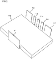
Fig. 2 is a perspective view illustrating an aspect in which a sealing part is removed in the semiconductor device according to the embodiment of the present invention. -
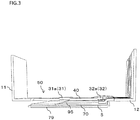
Fig. 3 is a side view of the aspect illustrated inFig. 2 as seen from the side. -
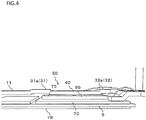
Fig. 4 is an enlarged side view ofFig. 3 . -
Fig. 5 is a bottom view illustrating a relationship of a head part, an avoiding part and the like used in the embodiment of the present invention. -
Fig. 6 is a side view illustrating a first example of a relationship of the head part, the avoiding part, a first main terminal, a front surface side sensing terminal and the like used in the embodiment of the present invention. -
Fig. 7 is a side view illustrating a second example of the relationship of the head part, the avoiding part, the first main terminal, the front surface side sensing terminal and the like used in the embodiment of the present invention. -
Fig. 8 is a side view illustrating a third example of the relationship of the head part, the avoiding part, the first main terminal, the front surface side sensing terminal and the like used in the embodiment of the present invention. -
Fig. 9 is a side view illustrating an aspect in which a connecting unit and the front surface side sensing terminal are separated. - As illustrated in
Fig. 2 , a semiconductor device being an example of an electronic device of this embodiment may have a sealing part 90 (refer toFig. 1 ) made of a sealing resin and the like, a firstmain terminal 11 being a first terminal projecting outward from a first side surface of thesealing part 90, asensing terminal 13 being a second terminal projecting outward from a second side surface different from the first side surface of the sealingpart 90, asemiconductor element 95 provided inside the sealingpart 90, and ahead part 40 coupled to the firstmain terminal 11 and thesensing terminal 13 and connected to a front surface of thesemiconductor element 95 via aconductive adhesive 75. In this embodiment, the firstmain terminal 11 through which main current flows is described as the first terminal, and thesensing terminal 13 on a front surface side used for sensing on a source side (hereinafter referred to as "front surfaceside sensing terminal 13") is described as the second terminal, but there is no limitation. It is also possible to adopt an aspect in which the main current does not flow through the first terminal or to use an aspect in which the second terminal is not used for the sensing. Also, in this embodiment, "coupled" also includes an "integrated" aspect. - Although the semiconductor device is used as the electronic device, and the
semiconductor element 95 is described as an electronic element in this embodiment, there is no limitation, and a "semiconductor" is not especially required. - The semiconductor device of this embodiment also has a second
main terminal 12 projecting outward from the sealingpart 90 through which the main current flows. Thesemiconductor element 95 illustrated inFig. 2 is such that the front surface is electrically connected to the firstmain terminal 11 and a back surface is electrically connected to the secondmain terminal 12. In this embodiment, thehead part 40 and the firstmain terminal 11 may be integrally formed, or thehead part 40 and the front surfaceside sensing terminal 13 may be integrally formed with a connectingunit 35. Also, the firstmain terminal 11, thehead part 40, the connectingunit 35, and the front surfaceside sensing terminal 13 may be integrally formed in this order. - Also, it is not limited to such an aspect; for example, the connecting
unit 35 and thehead part 40 are integrally formed, but the connectingunit 35 and the front surfaceside sensing terminal 13 may be separately formed. As an example, as illustrated inFig. 9 , a back surface of the connectingunit 35 may be coupled to a front surface of the front surfaceside sensing terminal 13 via a conductive adhesive and the like. Also, the firstmain terminal 11 and thehead part 40 are originally separated from each other and may be coupled to each other by using theconductive adhesive 75 and the like. - As illustrated in
Fig. 2 , the semiconductor device may have, for example, asubstrate 5 made of an insulating material and aconductor layer 70 made of copper and the like provided on thesubstrate 5. In an aspect illustrated inFig. 2 , the secondmain terminal 12 is connected to theconductor layer 70, and the secondmain terminal 12 is connected to the back surface of thesemiconductor element 95 via theconductor layer 70. A resist (not illustrated) may also be provided on a peripheral edge of a connecting portion of the secondmain terminal 12 to theconductor layer 70 in order to prevent the conductive adhesive such as solder from flowing. The back surface of thesemiconductor element 95 and theconductor layer 70 may also be connected via the conductive adhesive such as solder. Thehead part 40 and the front surface of thesemiconductor element 95 may also be connected to each other via the conductive adhesive 75 such as solder (refer toFig. 4 ). Also, aheat radiation plate 79 made of copper and the like may be provided on a back surface of thesubstrate 5. - The
semiconductor element 95 may have a withstand voltage structure such as a guard ring. In a case where thesemiconductor element 95 has such withstand voltage structure, avoidingparts head part 40 for avoiding contact with the withstand voltage structure may be provided as illustrated inFigs. 6 to 8 . Such avoidingparts semiconductor element 95 and designed in advance on the basis of an arrangement position of the withstand voltage structure such as the guard ring, a thickness in a planar direction thereof and the like. - The avoiding
parts part 31 provided between the firstmain terminal 11 and thehead part 40 and a second avoidingpart 32 provided between the front surfaceside sensing terminal 13 and thehead part 40. The first avoidingpart 31 may be a firstconcave part 31a concaved so as to be separated from thesemiconductor element 95 and the second avoidingpart 32 may be a secondconcave part 32a concaved so as to be separated from thesemiconductor element 95. - The first
main terminal 11 and the secondmain terminal 12 may be power terminals through which large-capacity current flows. - The
conductor layer 70 may not be provided below the firstmain terminal 11, the first avoidingpart 31 may be exposed outside from the side surface of the sealingpart 90 in the middle of the first avoidingpart 31, and the firstmain terminal 11 may be exposed outside from the side surface of the sealingpart 90 just after the first avoidingpart 31. - In a case where the first
main terminal 11 and thehead part 40 are integrally formed and the front surfaceside sensing terminal 13, the connectingunit 35, and thehead part 40 are integrally formed, a back surface side height of the firstmain terminal 11 may correspond to a back surface side height of the front surfaceside sensing terminal 13 as illustrated inFigs. 6 to 8 . Herein, when the heights correspond to each other, this means that they coincide with each other with difference within a range of 10% of a thickness of a thicker terminal out of the firstmain terminal 11 and the front surfaceside sensing terminal 13. In a case where a thickness T0 of the firstmain terminal 11 and that of the front surfaceside sensing terminal 13 are the same, difference between the back surface side height of the firstmain terminal 11 and the back surface side height of the secondmain terminal 12 is not larger than 10% of the thickness T0, which means that this is not larger than 0.1 T0. In a case where the thicknesses of the firstmain terminal 11 and the front surfaceside sensing terminal 13 are different from each other, the difference therebetween is not larger than 10% of a thickness T1 of the thicker one, which means that this is not larger than 0.1 T1. The back surface side height of the firstmain terminal 11 and the back surface side height of the front surfaceside sensing terminal 13 may coincide with each other. In a case of coincidence, this means that the difference between the back surface side height of the firstmain terminal 11 and the back surface side height of the front surfaceside sensing terminal 13 is within a manufacturing error range. - Also, in a case where the first
main terminal 11 and thehead part 40 are integrally formed and the connectingunit 35 and thehead part 40 are integrally formed as illustrated inFig. 9 , the back surface side height of the firstmain terminal 11 and the back surface side height of the front surfaceside sensing terminal 13 coupled to the connectingunit 35 may correspond to each other. Herein, when the heights correspond to each other, this means that they coincide with each other with difference within a range of 10% of the thickness of the thicker terminal out of the firstmain terminal 11 and the front surfaceside sensing terminal 13 as in the above-described aspect. The back surface side height of the firstmain terminal 11 and the back surface side height of the front surfaceside sensing terminal 13 may coincide with each other. In a case of coincidence, this means that the difference between the back surface side height of the firstmain terminal 11 and the back surface side height of the front surfaceside sensing terminal 13 is within a manufacturing error range. - The front surface
side sensing terminal 13 and the connectingunit 35, and the firstmain terminal 11 may be provided so as to extend in opposite directions from thehead part 40. It is sufficient that the front surfaceside sensing terminal 13 and the connectingunit 35, and the firstmain terminal 11 extend in the different directions as seen from thehead part 40, and there is no limitation. For example, the front surfaceside sensing terminal 13 and the connectingunit 35, and the firstmain terminal 11 may extend so as to form an angle (obtuse angle) of 90 degrees or larger. - As illustrated in
Figs. 5 ,6 , and8 , thehead part 40 may have a secondconvex part 42 projecting toward thesemiconductor element 95 and a firstconvex part 41 projecting from the secondconvex part 42 toward thesemiconductor element 95. As illustrated inFig. 7 , the secondconvex part 42 may not be provided and only the firstconvex part 41 may be provided. - In the aspect illustrated in
Fig. 2 , as an example, widths of the first avoidingpart 31, thehead part 40, and the second avoidingpart 32 are larger than widths of the front surfaceside sensing terminal 13 and the connectingunit 35, and widths of the firstmain terminal 11 and the secondmain terminal 12 are larger than the widths of the first avoidingpart 31, thehead part 40, and the second avoidingpart 32. - Regarding a sensing current path, it is not necessary to apply large-capacity current, so that the widths of the second avoiding
part 32, the connectingunit 35, and the front surfaceside sensing terminal 13 may be narrow. As an example, the width of each of the second avoidingpart 32, the connectingunit 35, and the front surfaceside sensing terminal 13 is narrowed; this may be one-third or less, or one-fifth or less of the width of thehead part 40. Meanwhile, in the aspect illustrated inFig. 2 , the width of the second avoidingpart 32 on a side of thehead part 40 is large, but such aspect is not needed. However, it is possible to surely secure the width of the planar-shapedhead part 40 of the second avoidingpart 32 by making the width of the second avoidingpart 32 on thehead part 40 side large and allowing the width of thehead part 40 side to correspond to the width of thehead part 40 as illustrated inFig. 2 . That is, when forming thehead part 40, the second avoidingpart 32 and the like, it is conceivable to punch out a conductive member such as a copper plate, but from a viewpoint of surely securing the width of thehead part 40, it is preferable that the width of the second avoidingpart 32 adjacent to thehead part 40 is made approximately the same as the width of thehead part 40. On the other hand, in a case of sacrificing the width of thehead part 40 to some extent, it is conceivable to make the width of an entire second avoidingpart 32 narrow. - In an aspect illustrated in
Fig. 1 , the secondmain terminal 12, the front surfaceside sensing terminal 13, a back surfaceside sensing terminal 14, and acontrol terminal 15 project from outside from the side surface on one side of the sealingpart 90, and the first main terminal 11 projects outward from the side surface on the other side of the sealingpart 90. The firstmain terminal 11, the secondmain terminal 12, the front surfaceside sensing terminal 13, the back surfaceside sensing terminal 14, and thecontrol terminal 15 are bent toward the front surface side to be connected to thecontrol substrate 5 provided on the front surface side. Thecontrol substrate 5 is used for controlling thesemiconductor element 95. - An inner structure of the sealing
part 90 of the semiconductor device may be line-symmetric. As an example, each of the firstmain terminal 11, the secondmain terminal 12, the front surfaceside sensing terminal 13, the back surfaceside sensing terminal 14, thecontrol terminal 15, and theconductor layer 70 may be arranged so as to be symmetric with respect to an arbitrary straight line. Meanwhile, awire 19 is also illustrated inFig. 2 . - Operations and effects according to this embodiment having the above-described configuration are next described.
- In this embodiment, as illustrated in
Fig. 2 and the like, the firstmain terminal 11 being the first terminal and the front surfaceside sensing terminal 13 being the second terminal extending in the direction different from that of the first terminal are coupled to thehead part 40, so that the firstmain terminal 11 and the front surfaceside sensing terminal 13 can be utilized as jig receivers. Therefore, it is possible to prevent the thickness of the conductive adhesive 75 such as solder provided on the front surface of thesemiconductor element 95 from becoming thin due to a weight of the connectingunit 35 by adjusting the heights of the back surface of the firstmain terminal 11 and the back surface of the front surfaceside sensing terminal 13 by usingjigs 99 and the like and sealing the same with the sealing resin and the like as illustrated inFigs. 6 to 8 . - In a case where the aspect in which the front surface
side sensing terminal 13, the connectingunit 35, and thehead part 40 are integrally formed is adopted as illustrated inFig. 2 and the like, it is possible to prevent height positions thereof from changing due to the coupling aspect of the front surfaceside sensing terminal 13 and the connectingunit 35 and to more accurately adjust the height by thejig 99 and the like. Therefore, an appropriate amount of the conductive adhesive 75 can be positioned between the front surface of thesemiconductor element 95 and thehead part 40, so that it is possible to more surely prevent cracking and the like due to a thinned thickness of theconductive adhesive 75. In a case of adopting an aspect in which the firstmain terminal 11 and thehead part 40 are integrally formed also, it is possible to prevent the height positions thereof from changing due to the coupling aspect of the firstmain terminal 11 and thehead part 40 and the height adjustment by thejig 99 and the like can be performed more accurately. - Also in a case where the
head part 40 and the connectingunit 35 are integrally formed, and the connectingunit 35 and the front surfaceside sensing terminal 13 are separately formed as illustrated inFig. 9 , it is possible to prevent the height positions thereof from changing due to the coupling aspect of thehead part 40 and the connectingunit 35 and to more accurately adjust the height by thejig 99 and the like. - As illustrated in
Fig. 3 , theconnection body 50 is in contact with thesemiconductor element 95 only with thehead part 40, and is provided apart from thesubstrate 5 in other portions, so that it is conceivable that theconductor layer 70 is not provided on the back surface side of the firstmain terminal 11. When such an aspect is adopted, a manufacturing cost can be reduced. Also, in a case where the firstmain terminal 11 and thehead part 40 are integrally formed, it is possible to expose the terminal outward from the side surface of the sealingpart 90 without intervention of theconductor layer 70, so that it is expected that a size in an in-plane direction is reduced because of absence of theconductor layer 70. It is also conceivable to adopt an aspect in which thesubstrate 5 itself is not provided on the back surface side of the firstmain terminal 11. When such aspect is adopted, it is possible to expect further reduction in manufacturing cost, and it is also possible to expect reduction in size in a planar direction of the semiconductor device. - In a case where the aspect in which the front surface
side sensing terminal 13 and the connectingunit 35, and the firstmain terminal 11 are provided so as to extend in the opposite directions from thehead part 40 as illustrated inFig. 2 and the like is adopted, it is possible to perform positioning by thejigs 99 in a stable state. Therefore, it is possible to improve operation efficiency and to reduce the possibility that thehead part 40 is erroneously inclined with respect to the front surface of thesemiconductor element 95. - When an aspect in which the back surface side height of the first
main terminal 11 corresponds to the back surface side height of the front surfaceside sensing terminal 13 is adopted as illustrated inFigs. 6 to 8 , operation of finely adjusting thejig 99 can be reduced, and it is possible to efficiently perform the positioning. It is also possible to reduce the possibility that thehead part 40 is erroneously inclined with respect to the front surface of thesemiconductor element 95. From the viewpoint of these effects, it is preferable that the difference between the back surface side height of the firstmain terminal 11 and the back surface side height of the front surfaceside sensing terminal 13 is not larger than 5% of the thickness T0 or T1, it is more preferable that this is not larger than 3% of the thickness To, and it is still more preferable that this is not larger than 1% of the thickness T0 or T1. - If the
semiconductor element 95 has the withstand voltage structure, in a case where the avoidingparts Fig. 2 and the like, it is possible to prevent electric contact of the withstand voltage structure of thesemiconductor element 95 and theconnection body 50. Also, in this aspect, in a case of adopting an aspect in which thehead part 40 is integrally formed with the firstmain terminal 11, the connectingunit 35, and the front surface side sensing terminal 13 (which may include the avoidingparts 31 and 32), it is possible to prevent the height positions thereof from changing due to the coupling aspect thereof and to more accurately adjust the height by thejig 99 and the like. - In a case where the avoiding
parts part 31 provided between the firstmain terminal 11 and thehead part 40 and the second avoidingpart 32 provided between the front surfaceside sensing terminal 13 and thehead part 40, it is useful in that electrical contact with the withstand voltage structure provided over a full circle such as the guard ring can be more surely prevented. - In a case of adopting an aspect in which the first avoiding
part 31 is the firstconcave part 31a and the second avoidingpart 32 is the secondconcave part 32a, it is useful in that the back surface side height of the firstmain terminal 11 and the back surface side height of the front surfaceside sensing terminal 13 can more easily correspond to each other and the operation efficiency can be improved. - In a case of adopting the aspect in which the
head part 40 has the firstconvex part 41 projecting toward thesemiconductor element 95 as illustrated inFig. 5 and the like, in a portion where the firstconvex part 41 is not provided, the thickness of the conductive adhesive 75 such as solder can be more surely made equal to or larger than a predetermined thickness. Meanwhile, the firstconvex part 41 may be in contact with the front surface of thesemiconductor element 95 or not. - In a case where an aspect in which the
head part 40 has the firstconvex part 41 and the secondconvex part 42 projecting toward thesemiconductor element 95, a usage amount of the conductive adhesive 75 can be reduced, and further the secondconvex part 42 can also be used to secure the width of the current path. - A manufacturing method for the semiconductor device having the above-described configuration is next described. Although detailed description is omitted because this will be repetitive description, in the manufacturing method for the semiconductor device, any aspect described in
- The
connection body 50 having the sealingpart 90, the firstmain terminal 11 being the first terminal for projecting outward from the first side surface of the sealingpart 90, the front surfaceside sensing terminal 13 being the second terminal for projecting outward from the second side surface different from the first side surface of the sealingpart 90, and thehead part 40 coupled to the firstmain terminal 11 and the front surfaceside sensing terminal 13 and for being connected to the front surface of thesemiconductor element 95 via theconductive adhesive 75 is prepared (preparing step). - Next, the
conductive adhesive 75 is placed on thesemiconductor element 95 placed on theconductor layer 70 on the substrate 5 (conductive adhesive placing step). - Next, the first
main terminal 11 and the front surfaceside sensing terminal 13 are placed on thejigs 99 so that thehead part 40 is connected to the front surface of thesemiconductor element 95 via the conductive adhesive 75 (positioning step, refer toFigs. 6 to 8 ). Thereafter, theconductive adhesive 75 is cured, and theconnection body 50 is positioned on the semiconductor element 95 (conductive adhesive curing step). - Next, the
semiconductor element 95, theconductor layer 70 and the like are covered with a metal mold, and the sealing resin is poured into the metal mold. After that, the sealing resin is cured (sealing resin curing step) . - Next, various terminals such as the first
main terminal 11, the secondmain terminal 12, the front surfaceside sensing terminal 13, the back surfaceside sensing terminal 14, and thecontrol terminal 15 are cut at predetermined positions, and thereafter bent toward the front surface side (cutting/bending step, refer toFig. 1 ). - In this manner, the semiconductor device as illustrated in
Fig. 1 is manufactured. - Lastly, the description of the embodiment and the disclosure of the drawings described above are merely examples for explaining the invention described in the claims, and the invention described in the claims is not limited by the description of the embodiment or the disclosure of the drawings described above. In addition, the recitation of the claims at the original application is merely an example, and the recitation of the claims can be appropriately changed based on the description of the specification, the drawings, and the like.
-
- 11 First terminal (first main terminal)
- 13 Second terminal (front surface side sensing terminal)
- 31 First avoiding part
- 31a First concave part (first avoiding part)
- 32 Second avoiding part
- 32a Second concave part (second avoiding part)
- 40 Head part
- 50 Connection body
- 75 Conductive adhesive
- 90 Sealing part
- 95 Semiconductor element (electronic element)
Claims (9)
- An electronic device comprising:a sealing part;a first terminal projecting outward from a first side surface of the sealing part;a second terminal projecting outward from a second side surface different from the first side surface of the sealing part;an electronic element provided inside the sealing part; anda head part coupled to the first terminal and the second terminal and connected to a front surface of the electronic element via a conductive adhesive.
- The electronic device according to claim 1,
wherein the first terminal and the second terminal extend in opposite directions from the head part. - The electronic device according to claim 1 or 2,
wherein the electronic element has a withstand voltage structure,
the electronic device further comprises:a first avoiding part, provided between the first terminal and the head part, for avoiding contact with the withstand voltage structure; anda second avoiding part, provided between the second terminal and the head part, for avoiding contact with the withstand voltage structure. - The electronic device according to claim 3,
wherein the first avoiding part is a first concave part concaved so as to be separated from the electronic element and
wherein the second avoiding part is a second concave part concaved so as to be separated from the electronic element. - The electronic device according to any one of claims 1 to 4,
wherein the first terminal is a power terminal, and wherein the second terminal is a sensing terminal. - The electronic device according to any one of claims 1 to 5,
wherein a back surface side height of the first terminal corresponds to a back surface side height of the second terminal. - The electronic device according to any one of claims 1 to 6,
wherein the head part is integrally formed with the first terminal and the second terminal. - A connection body, used in an electronic device having a sealing part and an electronic element provided inside the sealing part, comprising:a first terminal projecting outward from a first side surface of the sealing part;a second terminal projecting outward from a second side surface different from the first side surface of the sealing part; anda head part coupled to the first terminal and the second terminal and connected to a front surface of the electronic element.
- A manufacturing method for an electronic device comprising;
a step of preparing a sealing part, a first terminal for projecting outward from a first side surface of the sealing part, a second terminal for projecting outward from a second side surface different from the first side surface of the sealing part, and a head part coupled to the first terminal and the second terminal and for being connected to a front surface of an electronic element via a conductive adhesive;
a step of placing the conductive adhesive on the electronic element; and
a step of placing the first terminal and the second terminal on a jig so that the head part is connected to the front surface of the electronic element via the conductive adhesive.
Applications Claiming Priority (1)
| Application Number | Priority Date | Filing Date | Title |
|---|---|---|---|
| PCT/JP2017/006029 WO2018150558A1 (en) | 2017-02-20 | 2017-02-20 | Electronic device, connector, and method for producing electronic device |
Publications (3)
| Publication Number | Publication Date |
|---|---|
| EP3588554A1 true EP3588554A1 (en) | 2020-01-01 |
| EP3588554A4 EP3588554A4 (en) | 2020-09-02 |
| EP3588554B1 EP3588554B1 (en) | 2024-10-09 |
Family
ID=62706293
Family Applications (1)
| Application Number | Title | Priority Date | Filing Date |
|---|---|---|---|
| EP17838112.5A Active EP3588554B1 (en) | 2017-02-20 | 2017-02-20 | Electronic device, connector, and method for producing electronic device |
Country Status (6)
| Country | Link |
|---|---|
| US (1) | US11404353B2 (en) |
| EP (1) | EP3588554B1 (en) |
| JP (1) | JP6349470B1 (en) |
| KR (1) | KR102048481B1 (en) |
| CN (1) | CN109075146A (en) |
| WO (1) | WO2018150558A1 (en) |
Family Cites Families (16)
| Publication number | Priority date | Publication date | Assignee | Title |
|---|---|---|---|---|
| JPS58119665A (en) | 1982-01-11 | 1983-07-16 | Hitachi Ltd | Semiconductor device and manufacture thereof |
| JPS6373946A (en) | 1986-09-18 | 1988-04-04 | 株式会社東芝 | Magnetic resonance imaging apparatus |
| JPS6373946U (en) * | 1986-10-31 | 1988-05-17 | ||
| JP3780061B2 (en) * | 1997-04-17 | 2006-05-31 | 株式会社日立製作所 | Surface mount semiconductor device |
| US6249041B1 (en) | 1998-06-02 | 2001-06-19 | Siliconix Incorporated | IC chip package with directly connected leads |
| KR20000057810A (en) * | 1999-01-28 | 2000-09-25 | 가나이 쓰토무 | Semiconductor device |
| US6307755B1 (en) * | 1999-05-27 | 2001-10-23 | Richard K. Williams | Surface mount semiconductor package, die-leadframe combination and leadframe therefor and method of mounting leadframes to surfaces of semiconductor die |
| JP3740116B2 (en) * | 2002-11-11 | 2006-02-01 | 三菱電機株式会社 | Molded resin encapsulated power semiconductor device and manufacturing method thereof |
| US9391005B2 (en) * | 2009-10-27 | 2016-07-12 | Alpha And Omega Semiconductor Incorporated | Method for packaging a power device with bottom source electrode |
| EP2690658B1 (en) * | 2011-03-24 | 2019-11-13 | Mitsubishi Electric Corporation | Power semiconductor module and power unit device |
| JP5267959B2 (en) * | 2011-05-30 | 2013-08-21 | 株式会社デンソー | Semiconductor module and driving device using the same |
| JP2015012065A (en) | 2013-06-27 | 2015-01-19 | 株式会社デンソー | Manufacturing method of semiconductor device |
| US9472538B2 (en) | 2013-07-04 | 2016-10-18 | Mitsubishi Electric Corporation | Semiconductor device manufacturing method and semiconductor device |
| WO2016084483A1 (en) * | 2014-11-27 | 2016-06-02 | 新電元工業株式会社 | Lead frame, semiconductor device, method for manufacturing lead frame, and method for manufacturing semiconductor device |
| JP6522402B2 (en) * | 2015-04-16 | 2019-05-29 | ローム株式会社 | Semiconductor device |
| US10109617B2 (en) * | 2016-07-21 | 2018-10-23 | Samsung Electronics Co., Ltd. | Solid state drive package |
-
2017
- 2017-02-20 US US15/751,845 patent/US11404353B2/en active Active
- 2017-02-20 CN CN201780003204.2A patent/CN109075146A/en active Pending
- 2017-02-20 WO PCT/JP2017/006029 patent/WO2018150558A1/en not_active Ceased
- 2017-02-20 KR KR1020187008203A patent/KR102048481B1/en active Active
- 2017-02-20 EP EP17838112.5A patent/EP3588554B1/en active Active
- 2017-02-20 JP JP2017555413A patent/JP6349470B1/en active Active
Also Published As
| Publication number | Publication date |
|---|---|
| JPWO2018150558A1 (en) | 2019-02-21 |
| KR20180105629A (en) | 2018-09-28 |
| CN109075146A (en) | 2018-12-21 |
| US11404353B2 (en) | 2022-08-02 |
| KR102048481B1 (en) | 2019-11-25 |
| EP3588554B1 (en) | 2024-10-09 |
| WO2018150558A1 (en) | 2018-08-23 |
| JP6349470B1 (en) | 2018-06-27 |
| EP3588554A4 (en) | 2020-09-02 |
| US20200219797A1 (en) | 2020-07-09 |
Similar Documents
| Publication | Publication Date | Title |
|---|---|---|
| US10490379B2 (en) | Surface mount fuse | |
| EP3226292B1 (en) | Lead frame, semiconductor device, method for manufacturing lead frame, and method for manufacturing semiconductor device | |
| US9476915B2 (en) | Magnetic field current sensors | |
| EP2793256B1 (en) | Semiconductor device manufacturing method | |
| US10117341B2 (en) | Controller and manufacturing method thereof | |
| WO2013054731A1 (en) | Power supply control apparatus and fabrication method for same | |
| US10512168B2 (en) | Electronic device and method of manufacturing the same | |
| US10251268B2 (en) | Circuit structure | |
| TW201617637A (en) | Hall sensor manufacturing method and Hall sensor and lens module | |
| US11404353B2 (en) | Electronic device, connection body, and manufacturing method for electronic device | |
| EP3584831B1 (en) | Electronic device, and connector | |
| US11211311B2 (en) | Electronic device and connection body | |
| US10910292B2 (en) | Electronic device and connection body | |
| US10453781B2 (en) | Semiconductor device | |
| CN107431055B (en) | Semiconductor device | |
| JP2016178202A (en) | Junction structure for circuit board and electronic component, electronic circuit board, and manufacturing method of circuit board | |
| EP3703119B1 (en) | Semiconductor device and method for manufacturing semiconductor device | |
| CN104283044A (en) | Connector | |
| CN104283022A (en) | Connector |
Legal Events
| Date | Code | Title | Description |
|---|---|---|---|
| STAA | Information on the status of an ep patent application or granted ep patent |
Free format text: STATUS: UNKNOWN |
|
| STAA | Information on the status of an ep patent application or granted ep patent |
Free format text: STATUS: THE INTERNATIONAL PUBLICATION HAS BEEN MADE |
|
| PUAI | Public reference made under article 153(3) epc to a published international application that has entered the european phase |
Free format text: ORIGINAL CODE: 0009012 |
|
| STAA | Information on the status of an ep patent application or granted ep patent |
Free format text: STATUS: REQUEST FOR EXAMINATION WAS MADE |
|
| 17P | Request for examination filed |
Effective date: 20180215 |
|
| AK | Designated contracting states |
Kind code of ref document: A1 Designated state(s): AL AT BE BG CH CY CZ DE DK EE ES FI FR GB GR HR HU IE IS IT LI LT LU LV MC MK MT NL NO PL PT RO RS SE SI SK SM TR |
|
| AX | Request for extension of the european patent |
Extension state: BA ME |
|
| DAV | Request for validation of the european patent (deleted) | ||
| DAX | Request for extension of the european patent (deleted) | ||
| R17P | Request for examination filed (corrected) |
Effective date: 20180215 |
|
| A4 | Supplementary search report drawn up and despatched |
Effective date: 20200803 |
|
| RIC1 | Information provided on ipc code assigned before grant |
Ipc: H01L 23/495 20060101ALI20200728BHEP Ipc: H01L 21/60 20060101ALI20200728BHEP Ipc: H01L 23/48 20060101AFI20200728BHEP |
|
| STAA | Information on the status of an ep patent application or granted ep patent |
Free format text: STATUS: EXAMINATION IS IN PROGRESS |
|
| 17Q | First examination report despatched |
Effective date: 20220125 |
|
| GRAP | Despatch of communication of intention to grant a patent |
Free format text: ORIGINAL CODE: EPIDOSNIGR1 |
|
| STAA | Information on the status of an ep patent application or granted ep patent |
Free format text: STATUS: GRANT OF PATENT IS INTENDED |
|
| INTG | Intention to grant announced |
Effective date: 20240531 |
|
| RIN1 | Information on inventor provided before grant (corrected) |
Inventor name: MORINAGA, YUJI Inventor name: UMEDA, SOICHIRO |
|
| GRAS | Grant fee paid |
Free format text: ORIGINAL CODE: EPIDOSNIGR3 |
|
| GRAA | (expected) grant |
Free format text: ORIGINAL CODE: 0009210 |
|
| STAA | Information on the status of an ep patent application or granted ep patent |
Free format text: STATUS: THE PATENT HAS BEEN GRANTED |
|
| AK | Designated contracting states |
Kind code of ref document: B1 Designated state(s): AL AT BE BG CH CY CZ DE DK EE ES FI FR GB GR HR HU IE IS IT LI LT LU LV MC MK MT NL NO PL PT RO RS SE SI SK SM TR |
|
| REG | Reference to a national code |
Ref country code: CH Ref legal event code: EP |
|
| REG | Reference to a national code |
Ref country code: DE Ref legal event code: R096 Ref document number: 602017085415 Country of ref document: DE |
|
| REG | Reference to a national code |
Ref country code: IE Ref legal event code: FG4D |
|
| REG | Reference to a national code |
Ref country code: LT Ref legal event code: MG9D |
|
| REG | Reference to a national code |
Ref country code: NL Ref legal event code: MP Effective date: 20241009 |
|
| REG | Reference to a national code |
Ref country code: AT Ref legal event code: MK05 Ref document number: 1731552 Country of ref document: AT Kind code of ref document: T Effective date: 20241009 |
|
| PG25 | Lapsed in a contracting state [announced via postgrant information from national office to epo] |
Ref country code: NL Free format text: LAPSE BECAUSE OF FAILURE TO SUBMIT A TRANSLATION OF THE DESCRIPTION OR TO PAY THE FEE WITHIN THE PRESCRIBED TIME-LIMIT Effective date: 20241009 |
|
| PG25 | Lapsed in a contracting state [announced via postgrant information from national office to epo] |
Ref country code: NL Free format text: LAPSE BECAUSE OF FAILURE TO SUBMIT A TRANSLATION OF THE DESCRIPTION OR TO PAY THE FEE WITHIN THE PRESCRIBED TIME-LIMIT Effective date: 20241009 |
|
| PG25 | Lapsed in a contracting state [announced via postgrant information from national office to epo] |
Ref country code: PT Free format text: LAPSE BECAUSE OF FAILURE TO SUBMIT A TRANSLATION OF THE DESCRIPTION OR TO PAY THE FEE WITHIN THE PRESCRIBED TIME-LIMIT Effective date: 20250210 Ref country code: HR Free format text: LAPSE BECAUSE OF FAILURE TO SUBMIT A TRANSLATION OF THE DESCRIPTION OR TO PAY THE FEE WITHIN THE PRESCRIBED TIME-LIMIT Effective date: 20241009 Ref country code: IS Free format text: LAPSE BECAUSE OF FAILURE TO SUBMIT A TRANSLATION OF THE DESCRIPTION OR TO PAY THE FEE WITHIN THE PRESCRIBED TIME-LIMIT Effective date: 20250209 |
|
| PG25 | Lapsed in a contracting state [announced via postgrant information from national office to epo] |
Ref country code: FI Free format text: LAPSE BECAUSE OF FAILURE TO SUBMIT A TRANSLATION OF THE DESCRIPTION OR TO PAY THE FEE WITHIN THE PRESCRIBED TIME-LIMIT Effective date: 20241009 |
|
| PG25 | Lapsed in a contracting state [announced via postgrant information from national office to epo] |
Ref country code: BG Free format text: LAPSE BECAUSE OF FAILURE TO SUBMIT A TRANSLATION OF THE DESCRIPTION OR TO PAY THE FEE WITHIN THE PRESCRIBED TIME-LIMIT Effective date: 20241009 |
|
| PG25 | Lapsed in a contracting state [announced via postgrant information from national office to epo] |
Ref country code: ES Free format text: LAPSE BECAUSE OF FAILURE TO SUBMIT A TRANSLATION OF THE DESCRIPTION OR TO PAY THE FEE WITHIN THE PRESCRIBED TIME-LIMIT Effective date: 20241009 |
|
| PG25 | Lapsed in a contracting state [announced via postgrant information from national office to epo] |
Ref country code: NO Free format text: LAPSE BECAUSE OF FAILURE TO SUBMIT A TRANSLATION OF THE DESCRIPTION OR TO PAY THE FEE WITHIN THE PRESCRIBED TIME-LIMIT Effective date: 20250109 |
|
| PG25 | Lapsed in a contracting state [announced via postgrant information from national office to epo] |
Ref country code: LV Free format text: LAPSE BECAUSE OF FAILURE TO SUBMIT A TRANSLATION OF THE DESCRIPTION OR TO PAY THE FEE WITHIN THE PRESCRIBED TIME-LIMIT Effective date: 20241009 Ref country code: GR Free format text: LAPSE BECAUSE OF FAILURE TO SUBMIT A TRANSLATION OF THE DESCRIPTION OR TO PAY THE FEE WITHIN THE PRESCRIBED TIME-LIMIT Effective date: 20250110 Ref country code: AT Free format text: LAPSE BECAUSE OF FAILURE TO SUBMIT A TRANSLATION OF THE DESCRIPTION OR TO PAY THE FEE WITHIN THE PRESCRIBED TIME-LIMIT Effective date: 20241009 |
|
| PG25 | Lapsed in a contracting state [announced via postgrant information from national office to epo] |
Ref country code: PL Free format text: LAPSE BECAUSE OF FAILURE TO SUBMIT A TRANSLATION OF THE DESCRIPTION OR TO PAY THE FEE WITHIN THE PRESCRIBED TIME-LIMIT Effective date: 20241009 |
|
| PG25 | Lapsed in a contracting state [announced via postgrant information from national office to epo] |
Ref country code: RS Free format text: LAPSE BECAUSE OF FAILURE TO SUBMIT A TRANSLATION OF THE DESCRIPTION OR TO PAY THE FEE WITHIN THE PRESCRIBED TIME-LIMIT Effective date: 20250109 |
|
| PG25 | Lapsed in a contracting state [announced via postgrant information from national office to epo] |
Ref country code: SM Free format text: LAPSE BECAUSE OF FAILURE TO SUBMIT A TRANSLATION OF THE DESCRIPTION OR TO PAY THE FEE WITHIN THE PRESCRIBED TIME-LIMIT Effective date: 20241009 |
|
| PG25 | Lapsed in a contracting state [announced via postgrant information from national office to epo] |
Ref country code: DK Free format text: LAPSE BECAUSE OF FAILURE TO SUBMIT A TRANSLATION OF THE DESCRIPTION OR TO PAY THE FEE WITHIN THE PRESCRIBED TIME-LIMIT Effective date: 20241009 |
|
| REG | Reference to a national code |
Ref country code: DE Ref legal event code: R097 Ref document number: 602017085415 Country of ref document: DE |
|
| PG25 | Lapsed in a contracting state [announced via postgrant information from national office to epo] |
Ref country code: EE Free format text: LAPSE BECAUSE OF FAILURE TO SUBMIT A TRANSLATION OF THE DESCRIPTION OR TO PAY THE FEE WITHIN THE PRESCRIBED TIME-LIMIT Effective date: 20241009 |
|
| PG25 | Lapsed in a contracting state [announced via postgrant information from national office to epo] |
Ref country code: RO Free format text: LAPSE BECAUSE OF FAILURE TO SUBMIT A TRANSLATION OF THE DESCRIPTION OR TO PAY THE FEE WITHIN THE PRESCRIBED TIME-LIMIT Effective date: 20241009 |
|
| PG25 | Lapsed in a contracting state [announced via postgrant information from national office to epo] |
Ref country code: SK Free format text: LAPSE BECAUSE OF FAILURE TO SUBMIT A TRANSLATION OF THE DESCRIPTION OR TO PAY THE FEE WITHIN THE PRESCRIBED TIME-LIMIT Effective date: 20241009 |
|
| PG25 | Lapsed in a contracting state [announced via postgrant information from national office to epo] |
Ref country code: CZ Free format text: LAPSE BECAUSE OF FAILURE TO SUBMIT A TRANSLATION OF THE DESCRIPTION OR TO PAY THE FEE WITHIN THE PRESCRIBED TIME-LIMIT Effective date: 20241009 |
|
| PG25 | Lapsed in a contracting state [announced via postgrant information from national office to epo] |
Ref country code: IT Free format text: LAPSE BECAUSE OF FAILURE TO SUBMIT A TRANSLATION OF THE DESCRIPTION OR TO PAY THE FEE WITHIN THE PRESCRIBED TIME-LIMIT Effective date: 20241009 |
|
| PLBE | No opposition filed within time limit |
Free format text: ORIGINAL CODE: 0009261 |
|
| STAA | Information on the status of an ep patent application or granted ep patent |
Free format text: STATUS: NO OPPOSITION FILED WITHIN TIME LIMIT |
|
| PG25 | Lapsed in a contracting state [announced via postgrant information from national office to epo] |
Ref country code: SE Free format text: LAPSE BECAUSE OF FAILURE TO SUBMIT A TRANSLATION OF THE DESCRIPTION OR TO PAY THE FEE WITHIN THE PRESCRIBED TIME-LIMIT Effective date: 20241009 |
|
| PG25 | Lapsed in a contracting state [announced via postgrant information from national office to epo] |
Ref country code: MC Free format text: LAPSE BECAUSE OF FAILURE TO SUBMIT A TRANSLATION OF THE DESCRIPTION OR TO PAY THE FEE WITHIN THE PRESCRIBED TIME-LIMIT Effective date: 20241009 |
|
| 26N | No opposition filed |
Effective date: 20250710 |
|
| REG | Reference to a national code |
Ref country code: CH Ref legal event code: PL |
|
| PG25 | Lapsed in a contracting state [announced via postgrant information from national office to epo] |
Ref country code: LU Free format text: LAPSE BECAUSE OF NON-PAYMENT OF DUE FEES Effective date: 20250220 |
|
| PG25 | Lapsed in a contracting state [announced via postgrant information from national office to epo] |
Ref country code: CH Free format text: LAPSE BECAUSE OF NON-PAYMENT OF DUE FEES Effective date: 20250228 |
|
| GBPC | Gb: european patent ceased through non-payment of renewal fee |
Effective date: 20250220 |
|
| REG | Reference to a national code |
Ref country code: DE Ref legal event code: R079 Ref document number: 602017085415 Country of ref document: DE Free format text: PREVIOUS MAIN CLASS: H01L0023480000 Ipc: H10W0072000000 |
|
| REG | Reference to a national code |
Ref country code: BE Ref legal event code: MM Effective date: 20250228 |
|
| PG25 | Lapsed in a contracting state [announced via postgrant information from national office to epo] |
Ref country code: GB Free format text: LAPSE BECAUSE OF NON-PAYMENT OF DUE FEES Effective date: 20250220 |
|
| PG25 | Lapsed in a contracting state [announced via postgrant information from national office to epo] |
Ref country code: FR Free format text: LAPSE BECAUSE OF NON-PAYMENT OF DUE FEES Effective date: 20250228 |
|
| PG25 | Lapsed in a contracting state [announced via postgrant information from national office to epo] |
Ref country code: BE Free format text: LAPSE BECAUSE OF NON-PAYMENT OF DUE FEES Effective date: 20250228 |
|
| PG25 | Lapsed in a contracting state [announced via postgrant information from national office to epo] |
Ref country code: IE Free format text: LAPSE BECAUSE OF NON-PAYMENT OF DUE FEES Effective date: 20250220 |
|
| PGFP | Annual fee paid to national office [announced via postgrant information from national office to epo] |
Ref country code: DE Payment date: 20260218 Year of fee payment: 10 |