EP3588552B1 - Feuille de matériau d'interface thermique et procédé de fabrication d'une feuille de matériau d'interface thermique - Google Patents
Feuille de matériau d'interface thermique et procédé de fabrication d'une feuille de matériau d'interface thermique Download PDFInfo
- Publication number
- EP3588552B1 EP3588552B1 EP19181121.5A EP19181121A EP3588552B1 EP 3588552 B1 EP3588552 B1 EP 3588552B1 EP 19181121 A EP19181121 A EP 19181121A EP 3588552 B1 EP3588552 B1 EP 3588552B1
- Authority
- EP
- European Patent Office
- Prior art keywords
- thermal interface
- interface material
- layer
- material sheet
- sensor
- Prior art date
- Legal status (The legal status is an assumption and is not a legal conclusion. Google has not performed a legal analysis and makes no representation as to the accuracy of the status listed.)
- Active
Links
Images
Classifications
-
- G—PHYSICS
- G01—MEASURING; TESTING
- G01D—MEASURING NOT SPECIALLY ADAPTED FOR A SPECIFIC VARIABLE; ARRANGEMENTS FOR MEASURING TWO OR MORE VARIABLES NOT COVERED IN A SINGLE OTHER SUBCLASS; TARIFF METERING APPARATUS; MEASURING OR TESTING NOT OTHERWISE PROVIDED FOR
- G01D21/00—Measuring or testing not otherwise provided for
- G01D21/02—Measuring two or more variables by means not covered by a single other subclass
-
- H—ELECTRICITY
- H05—ELECTRIC TECHNIQUES NOT OTHERWISE PROVIDED FOR
- H05K—PRINTED CIRCUITS; CASINGS OR CONSTRUCTIONAL DETAILS OF ELECTRIC APPARATUS; MANUFACTURE OF ASSEMBLAGES OF ELECTRICAL COMPONENTS
- H05K7/00—Constructional details common to different types of electric apparatus
- H05K7/20—Modifications to facilitate cooling, ventilating, or heating
- H05K7/2089—Modifications to facilitate cooling, ventilating, or heating for power electronics, e.g. for inverters for controlling motor
- H05K7/209—Heat transfer by conduction from internal heat source to heat radiating structure
-
- H—ELECTRICITY
- H10—SEMICONDUCTOR DEVICES; ELECTRIC SOLID-STATE DEVICES NOT OTHERWISE PROVIDED FOR
- H10W—GENERIC PACKAGES, INTERCONNECTIONS, CONNECTORS OR OTHER CONSTRUCTIONAL DETAILS OF DEVICES COVERED BY CLASS H10
- H10W40/00—Arrangements for thermal protection or thermal control
-
- F—MECHANICAL ENGINEERING; LIGHTING; HEATING; WEAPONS; BLASTING
- F28—HEAT EXCHANGE IN GENERAL
- F28F—DETAILS OF HEAT-EXCHANGE AND HEAT-TRANSFER APPARATUS, OF GENERAL APPLICATION
- F28F21/00—Constructions of heat-exchange apparatus characterised by the selection of particular materials
- F28F21/02—Constructions of heat-exchange apparatus characterised by the selection of particular materials of carbon, e.g. graphite
-
- F—MECHANICAL ENGINEERING; LIGHTING; HEATING; WEAPONS; BLASTING
- F28—HEAT EXCHANGE IN GENERAL
- F28F—DETAILS OF HEAT-EXCHANGE AND HEAT-TRANSFER APPARATUS, OF GENERAL APPLICATION
- F28F21/00—Constructions of heat-exchange apparatus characterised by the selection of particular materials
- F28F21/06—Constructions of heat-exchange apparatus characterised by the selection of particular materials of plastics material
-
- F—MECHANICAL ENGINEERING; LIGHTING; HEATING; WEAPONS; BLASTING
- F28—HEAT EXCHANGE IN GENERAL
- F28F—DETAILS OF HEAT-EXCHANGE AND HEAT-TRANSFER APPARATUS, OF GENERAL APPLICATION
- F28F21/00—Constructions of heat-exchange apparatus characterised by the selection of particular materials
- F28F21/08—Constructions of heat-exchange apparatus characterised by the selection of particular materials of metal
- F28F21/081—Heat exchange elements made from metals or metal alloys
-
- G—PHYSICS
- G01—MEASURING; TESTING
- G01K—MEASURING TEMPERATURE; MEASURING QUANTITY OF HEAT; THERMALLY-SENSITIVE ELEMENTS NOT OTHERWISE PROVIDED FOR
- G01K7/00—Measuring temperature based on the use of electric or magnetic elements directly sensitive to heat ; Power supply therefor, e.g. using thermoelectric elements
- G01K7/16—Measuring temperature based on the use of electric or magnetic elements directly sensitive to heat ; Power supply therefor, e.g. using thermoelectric elements using resistive elements
-
- G—PHYSICS
- G01—MEASURING; TESTING
- G01L—MEASURING FORCE, STRESS, TORQUE, WORK, MECHANICAL POWER, MECHANICAL EFFICIENCY, OR FLUID PRESSURE
- G01L1/00—Measuring force or stress, in general
- G01L1/18—Measuring force or stress, in general using properties of piezo-resistive materials, i.e. materials of which the ohmic resistance varies according to changes in magnitude or direction of force applied to the material
-
- H—ELECTRICITY
- H05—ELECTRIC TECHNIQUES NOT OTHERWISE PROVIDED FOR
- H05K—PRINTED CIRCUITS; CASINGS OR CONSTRUCTIONAL DETAILS OF ELECTRIC APPARATUS; MANUFACTURE OF ASSEMBLAGES OF ELECTRICAL COMPONENTS
- H05K7/00—Constructional details common to different types of electric apparatus
- H05K7/20—Modifications to facilitate cooling, ventilating, or heating
- H05K7/2039—Modifications to facilitate cooling, ventilating, or heating characterised by the heat transfer by conduction from the heat generating element to a dissipating body
-
- H—ELECTRICITY
- H10—SEMICONDUCTOR DEVICES; ELECTRIC SOLID-STATE DEVICES NOT OTHERWISE PROVIDED FOR
- H10W—GENERIC PACKAGES, INTERCONNECTIONS, CONNECTORS OR OTHER CONSTRUCTIONAL DETAILS OF DEVICES COVERED BY CLASS H10
- H10W40/00—Arrangements for thermal protection or thermal control
- H10W40/70—Fillings or auxiliary members in containers or in encapsulations for thermal protection or control
-
- H—ELECTRICITY
- H10—SEMICONDUCTOR DEVICES; ELECTRIC SOLID-STATE DEVICES NOT OTHERWISE PROVIDED FOR
- H10W—GENERIC PACKAGES, INTERCONNECTIONS, CONNECTORS OR OTHER CONSTRUCTIONAL DETAILS OF DEVICES COVERED BY CLASS H10
- H10W40/00—Arrangements for thermal protection or thermal control
- H10W40/20—Arrangements for cooling
- H10W40/25—Arrangements for cooling characterised by their materials
- H10W40/251—Organics
-
- H—ELECTRICITY
- H10—SEMICONDUCTOR DEVICES; ELECTRIC SOLID-STATE DEVICES NOT OTHERWISE PROVIDED FOR
- H10W—GENERIC PACKAGES, INTERCONNECTIONS, CONNECTORS OR OTHER CONSTRUCTIONAL DETAILS OF DEVICES COVERED BY CLASS H10
- H10W40/00—Arrangements for thermal protection or thermal control
- H10W40/20—Arrangements for cooling
- H10W40/25—Arrangements for cooling characterised by their materials
- H10W40/258—Metallic materials
Definitions
- the present invention relates generally to thermal interface materials.
- Power electronic devices employ high power switches or power electronic modules which are able to switch high currents and withstand high voltages.
- the switched high currents generate heat losses inside the component or module, and these losses are led to a base plate of the component or module.
- a cooling device is further thermally connected to the base plate for transferring the heat from the component to the surroundings.
- a typical example of a cooling device is a heatsink which has a surface that can be thermally connected to the surface of the base plate.
- the chip temperature refers to temperature of the semiconductor junction of the power electronic switch. It is challenging to measure the chip temperature directly and in practice it is estimated using a temperature reading from the module's baseplate directly under the chip of interest. This temperature is generally referred to as case temperature Tc. When the case temperature and the heat loss values are known, the chip temperature can be calculated using junction-to-case thermal resistance which is given by the component manufacturer. As a power electronic module has multiple of switch components, it is often required that the case temperature is measured in multiple of positions to obtain the temperature values of desired chips.
- thermocouples are easy to use with air cooled heatsinks where through-holes are easy to drill to the heatsink.
- their application becomes difficult with liquid and two-phase coolers where the coolant channel is often designed to run below the hottest chips i.e. where the sensor should be placed.
- the placement of the sensor is challenging into water cooled cold plates, base-to-air Cothex heat exchangers and heat pipe heatsinks. In such cooling devices some compromises need to be made over the sensor location in regard to the chip temperature of interest.
- the spring-loaded thermocouples provide accurate readings if the thermocouple is in direct contact with the base plate of the module.
- the material should be paste or grease. If solid thermal interface materials are employed, the material should be removed from the places where measurement is made. Otherwise the thermal interface material affects the measurement.
- Another issue with power electronic modules baseplate is the warping and bending of the baseplate during installation and use of the power electronic module. Especially if the use of the module or the device in which the module is situated is cyclic, the base plate may get out of its original shape. When the base plate is warped or bent, the transfer of heat from the module to the heatsink can be reduced such that the chip temperatures may rise to values which are not tolerable. The base plate's deviation from flatness may exceed 0.1 mm over the length of 50 mm during the use of the power electronic module.
- the deformation is mainly due to power cycling, temperature gradients and differences between thermal expansion coefficients. This dynamic behaviour causes complex deformation scenario to the thermal interface between the power electronic module and the heatsink.
- This deformation further may stress the thermal interface material between the power electronic module and the heatsink and may destroy the thermal interface material's capability to carry out the heat conduction function.
- power electronic modules may also experience permanent deformation during operation. However, the bending and deformation of the base plate cannot be determined during use of the power electronic module.
- An object of the present invention is thus to provide a structure and a method of manufacturing the structure so as to overcome the above problems.
- the objects of the invention are achieved by a thermal interface material sheet and a method of manufacturing such sheet which are characterized by what is stated in the independent claims.
- the preferred embodiments of the invention are disclosed in the dependent claims.
- the invention is based on the idea of providing thin film sensors in the structure of thermal interface material sheet.
- Thermal interface materials are placed between the heat generating component and the cooling device to enhance the transfer of heat from the component to the cooling device. Once a sensor is disposed in the thermal interface material sheet and the thermal interface material is between the heat generating component and the cooling device, it can be used to measure accurately a property, such as temperature or pressure, of the assembly.
- the thin film sensor is a physical vapour deposition (PVD) grown thin film sensor and the thermal interface material (TIM) sheet is preferably a carbon based sheet.
- the TIM sheet is partially coated with an electrically insulating layer to facilitate sensor manufacturing using PVD method.
- the thin film sensor is preferably a resistor based temperature sensor, piezo resistive strain gauge to measure pressure or a piezo resistive sensor for sensing both the temperature and pressure.
- the TIM-sheet of the present disclosure operates as a thermal interface material sheet for electronic components, such as power electronic modules, and at the same time is able to produce measurement data from the interconnection between the electronic component and the cooling element without affecting the transfer of heat.
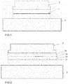
- Figure 1 shows the thermal interface material sheet 1 of the present disclosure in connection with a power electronic module 2 and a cooling device 3, such as a heat sink.
- the components of Figure 1 are shown separated from each other. However, it is clear that the power electric module 2 is attached tightly to the cooling device 3 with the thermal interface material between the module and the cooling device.
- the thermal interface material sheet comprises a carbon based layer, such as a graphite or graphene sheet 21.
- the carbon based layer 21 is at least partially coated with electrically insulating layer 22.
- electrically insulating layer include PET film or PVD ceramics.
- the thin film sensor 23 is grown on top of the insulating layer using PVD method, and a second electrically insulating layer 24 is placed on top of the sensor 23.
- the PVD grown sensor is a thin film strain sensor, it is beneficial to attach the TIM sheet firmly to the base surface of the power electronic module or similar heat generating component to achieve a higher measurement accuracy. Therefore the second insulating layer 24 may have an adhesive coating on the surface facing the base surface of the power electronic module.
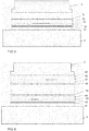
- FIG 3 shows another embodiment of the invention with a temperature sensor in the TIM sheet.
- the thermal interface material sheet of the example consists of a carbon based layer 31, which is at least partly covered with electrically insulating layer 32 on top of which a resistive temperature sensor 33 is grown with a PVD method.
- a resistive temperature sensor 33 is grown with a PVD method.
- a second electrically insulating layer 34 On top of the resistive temperature sensor is a second electrically insulating layer 34, which covers at least the sensor.
- the structure of the thermal interface material layer of the example of Figure 3 comprises also a lubricating top layer 35 which provides wear resistance to the structure.
- the lubricating layer may be achieved with a carbon based material, for example.
- Figure 4 shows another embodiment of the invention in which both a temperature sensor and a strain sensor are employed.
- the structure of the thermal interface material sheet of Figure 4 is basically combination of the sheets of Figures 2 and 3 .
- a carbon based thermal interface material layer 41 is provided.
- On top of the TIM layer 41 is disposed an electrically insulating layer 42 which covers the TIM layer at least partially.
- the insulating layer 42 has a PVD grown temperature sensor 43 which is covered with a second insulating layer 44.
- a carbon based material layer 45 On top of the insulating layer is a carbon based material layer 45 for providing lubrication and wear resistance.
- Figure 4 further shows a strain sensor assembly which is formed of a carbon based material sheet 46, electrically insulating layer 47 on top of which a strain gauge 48 is grown with PVD method.
- the uppermost layer is an electric insulating layer 49, such as a PET film with an adhesive on the surface facing the base of the heat generating component 2.
- the carbon based material sheet 46 is an optional layer as it is on top of a similar carbon based sheet 45.
- FIG. 5 shows another view of an embodiment of the present invention for better understanding the invention.
- a graphite sheet 51 is provided and an electrically insulating layer 52 is set on top of the graphite sheet 51.
- the electrically insulating layer is not covering the graphite sheet 51 completely as the purpose of the insulating layer is to be a base for the PVD grown sensor 53.
- a second electrically insulating layer 54 is placed on top of the sensor 53, and a wear resistant layer 55 is provided on top of the second insulating layer.
- the graphite sheet or layer 51 has a surface area that is larger than the surface areas of the other layers.
- base plate of the component or module may be formed of electrically insulating material, such as ceramic material.
- the insulating layer on top of the graphite sheet is not required.
- the surface of the cooling device may also be coated with an electrically insulating material, which also reduces the need of insulating layers in the thermal interface material sheet.
- the coating may be a ceramic coating or anodised coating when the cooling device is of aluminium.
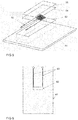
- Figure 6 shows a different view of a simplified structure of the invention with the sensor and its electrical connectors visible.
- the structure shows a planar view of a carbon based material layer 61, a sensor 62 and the electrical conductors of the sensor.
- the electrical conductors needed for the sensor are also manufactured on the insulating layer with the same technology as the sensor.
- the sensor is an electrical component and the electrical properties of the component are changed due to change of temperature or pressure depending on the type of sensor.
- the information obtained with the sensors is readily available in other circuits.
- the temperature and pressure information can be used in real time when the device employing the structure of the invention is used. Based on the temperature and the pressure information the condition of the cooling of the device may be monitored. If the measurements show that a measured temperature is rising above a set limit, an alarm may be given and the device may be turned off in a controlled manner.
- the strain sensor in the thermal interface material layer may be used for providing indication of changed conditions. If the pressure between the cooling device and the base of the power electronic module decreases, it is an indication of a change that will affect the cooling properties.
- only one sensor is disposed on one layer.
- multiple of sensors can be manufactured on the same electrically insulating layer.
- the sensors may be of the same or different type. This, for example, enables to measure temperature in different locations under the base of the power electronic module. Further, multiple of sensors in one layer enables to simplify the construction as the number of different layers is minimized.
- the thermal interface material layer of the invention acts as a normal thermal interface and can be used in connection with any type of cooling device.
- the cooling device does not need any modifications for measurement of temperature or pressure.
- the thermal interface material layer is preferably made of 70 to 200 ⁇ m thick carbon layer and the insulating layer on top of the carbon layer is, for example 10 ⁇ m thick PET film or PVD ceramics layer.
- the PVD manufacturing method is known as such, and the manufacturing of the sensors using PVD method is not specifically described here.
- the PVD method is used as an example of a suitable method for producing thin film sensors.
- the low temperature PVD technology is the most suitable for growing thin film sensors and conductors on an electrically insulating polyimide films.
- Other suitable method or technologies include chemical vapour deposition (CVD) and ink-jet technology.
- thermal interface material is described to be carbon based material, such as graphite.
- graphite may be a preferred material
- the material can also be a thin metal sheet, multilayer thermally conducting silicone rubber or aluminium sheet structure.
- the requirement for the thermal interface material is that it is solid enough to support the thin film structure disposed in the thermal interface material sheet of the invention.
- the structure of the invention is shown as separate layers. However, it is clear that a single sheet is formed of the separate layers. Further the sensors are illustrated as separate layers in the attached drawings. The sensors are however grown on the insulating layer and are therefore one single structure.
- Figures 2 and 3 are used in the following to illustrate the method of manufacturing a thermal interface material sheet.
- a thermal interface material layer 21 is provided.
- a thin film sensor 23, such as a resistive sensor or a strain gauge sensor is disposed on an electrically insulating 22 layer.
- the thin film sensor is grown on the electrically insulating film or layer usig PVD method which known as such.
- a second electrically insulating layer 24 is disposed on top of the sensor for producing a thermal interface material sheet.
- the second electrically insulating layer is provided with an adhesive layer.
- a lubricating layer is disposed on top of the second electrically insulating layer to provide wear resistance.
- the invention relates also to an electrical device, such as an inverter or a frequency converter, which comprises one or more power electronic modules.
- the electronic device of the invention comprises a cooling device, such as a heat sink thermally connected to a power electronic module.
- a thermal interface material sheet of the invention is disposed between the cooling device and the power electronic module. Further, the electrical connectors of the thermal interface material layer are electrically connected to the electrical circuitry of the electronic device for obtaining information relating to the operation of the cooling device.
Landscapes
- Engineering & Computer Science (AREA)
- Physics & Mathematics (AREA)
- Thermal Sciences (AREA)
- Mechanical Engineering (AREA)
- General Engineering & Computer Science (AREA)
- General Physics & Mathematics (AREA)
- Microelectronics & Electronic Packaging (AREA)
- Cooling Or The Like Of Semiconductors Or Solid State Devices (AREA)
- Cooling Or The Like Of Electrical Apparatus (AREA)
Claims (15)
- Feuille de matériau d'interface thermique (1) devant être disposée entre un composant électrique générant de la chaleur (2) et un dispositif de refroidissement (3), la feuille de matériau d'interface thermique comprenant au moins un capteur en couche mince (23) et des conducteurs électriques reliés à l'au moins un capteur en couche mince pour mesurer une propriété associée au composant électrique générant de la chaleur, caractérisé en ce que l'au moins un capteur en couche mince (23) est un capteur élaboré par dépôt physique en phase vapeur (PVD).
- Feuille de matériau d'interface thermique selon la revendication 1, dans laquelle les conducteurs électriques sont des conducteurs élaborés par dépôt physique en phase vapeur.
- Feuille de matériau d'interface thermique selon la revendication 1, la feuille de matériau d'interface thermique comprenant une couche de matériau d'interface thermique, une couche électriquement isolante (22) sur laquelle est disposé l'au moins un capteur en couche mince (23), et une deuxième couche électriquement isolante (24) au-dessus de l'au moins un capteur en couche mince.
- Feuille de matériau d'interface thermique selon la revendication 3, dans laquelle la deuxième couche électriquement isolante comprend un adhésif au-dessus de la couche pour fixation à une base du composant électrique générant de la chaleur.
- Feuille de matériau d'interface thermique selon la revendication 3, la feuille de matériau d'interface thermique comprenant en outre une couche lubrifiante au-dessus de la deuxième couche électriquement isolante pour apporter une résistance à l'usure.
- Feuille de matériau d'interface thermique selon la revendication 4, dans laquelle la couche de matériau d'interface thermique est une couche à base de carbone, une couche d'interface thermique en fine tôle métallique ou une couche de caoutchouc de silicone thermoconductrice multicouche.
- Feuille de matériau d'interface thermique selon la revendication 6, dans laquelle la couche de matériau d'interface thermique a une plus grande superficie que les couches isolantes.
- Feuille de matériau d'interface thermique selon la revendication 3, dans laquelle le capteur est un capteur de température ou une jauge de contrainte.
- Procédé de fabrication d'une feuille de matériau d'interface thermique, le procédé comprenant l'obtention d'une couche de matériau d'interface thermique, l'application d'une couche électriquement isolante (22), la disposition sur la couche électriquement isolante d'au moins un capteur en couche mince (23), et l'application d'une deuxième couche électriquement isolante (24) au-dessus de l'au moins un capteur en couche mince, caractérisé en ce que l'au moins un capteur en couche mince est un capteur élaboré par dépôt physique en phase vapeur (PVD).
- Procédé selon la revendication 9, le procédé comprenant en outre l'application d'une couche adhésive au-dessus de la deuxième couche électriquement isolante.
- Procédé selon la revendication 9, le procédé comprenant en outre l'application d'une couche lubrifiante au-dessus de la deuxième couche électriquement isolante.
- Dispositif électrique comprenant un module électronique de puissance (2) et un dispositif de refroidissement (3), dans lequel une feuille de matériau d'interface thermique ayant au moins un capteur en couche mince (23) et des conducteurs électriques reliés à l'au moins un capteur en couche mince pour mesurer une propriété associée au composant électrique générant de la chaleur est disposée entre une base du module électronique de puissance et le dispositif de refroidissement, et les conducteurs électriques sont reliés au circuit électrique du dispositif électrique, caractérisé en ce que l'au moins un capteur en couche mince est un capteur élaboré par dépôt physique en phase vapeur (PVD).
- Dispositif électrique selon la revendication 12, le dispositif électrique étant un convertisseur de fréquence ou un onduleur.
- Feuille de matériau d'interface thermique selon la revendication 5, dans laquelle la couche de matériau d'interface thermique est une couche à base de carbone, une couche d'interface thermique en fine tôle métallique ou une couche de caoutchouc de silicone thermoconductrice multicouche.
- Feuille de matériau d'interface thermique selon la revendication 14, dans laquelle la couche de matériau d'interface thermique a une plus grande superficie que les couches isolantes.
Applications Claiming Priority (1)
| Application Number | Priority Date | Filing Date | Title |
|---|---|---|---|
| US16/014,684 US20190394898A1 (en) | 2018-06-21 | 2018-06-21 | Thermal interface material sheet and method of manufacturing a thermal interface material sheet |
Publications (2)
| Publication Number | Publication Date |
|---|---|
| EP3588552A1 EP3588552A1 (fr) | 2020-01-01 |
| EP3588552B1 true EP3588552B1 (fr) | 2021-04-28 |
Family
ID=67001551
Family Applications (1)
| Application Number | Title | Priority Date | Filing Date |
|---|---|---|---|
| EP19181121.5A Active EP3588552B1 (fr) | 2018-06-21 | 2019-06-19 | Feuille de matériau d'interface thermique et procédé de fabrication d'une feuille de matériau d'interface thermique |
Country Status (3)
| Country | Link |
|---|---|
| US (1) | US20190394898A1 (fr) |
| EP (1) | EP3588552B1 (fr) |
| CN (1) | CN110631630A (fr) |
Families Citing this family (7)
| Publication number | Priority date | Publication date | Assignee | Title |
|---|---|---|---|---|
| US11778722B2 (en) * | 2021-05-04 | 2023-10-03 | Gm Cruise Holdings Llc | Autonomous vehicle computing device with barrier layer |
| JP2023111629A (ja) * | 2022-01-31 | 2023-08-10 | パナソニックIpマネジメント株式会社 | 電気機器 |
| US20240014093A1 (en) * | 2022-07-06 | 2024-01-11 | STATS ChipPAC Pte. Ltd. | Semiconductor Device and Method of Heat Dissipation Using Graphene |
| US12564059B2 (en) | 2022-10-12 | 2026-02-24 | STATS ChipPAC Pte. Ltd. | Semiconductor device and method of forming graphene core shell embedded within shielding layer |
| US12581974B2 (en) | 2023-01-05 | 2026-03-17 | STATS ChipPAC Pte. Ltd. | Semiconductor device and method of making a semiconductor package with graphene-coated interconnects |
| US12588572B2 (en) | 2023-03-15 | 2026-03-24 | STATS ChipPAC Pte. Ltd. | Semiconductor device and method of forming fine pitch conductive posts with graphene-coated cores |
| EP4517812A3 (fr) * | 2023-09-04 | 2025-03-19 | BSH Hausgeräte GmbH | Dispositif d'appareil ménager, appareil ménager et procédé de fabrication du dispositif d'appareil ménager |
Family Cites Families (5)
| Publication number | Priority date | Publication date | Assignee | Title |
|---|---|---|---|---|
| DE10225602A1 (de) * | 2002-06-07 | 2004-01-08 | Heraeus Sensor-Nite Gmbh | Halbleiterbauelement mit integrierter Schaltung, Kühlkörper und Temperatursensor |
| US7262509B2 (en) * | 2004-05-11 | 2007-08-28 | Intel Corporation | Microelectronic assembly having a perimeter around a MEMS device |
| EP3096351B1 (fr) * | 2015-05-22 | 2017-12-13 | ABB Technology Oy | Film d'interface thermique |
| EP3163611B1 (fr) * | 2015-11-02 | 2021-06-30 | ABB Schweiz AG | Ensemble électronique de puissance |
| US20180134925A1 (en) * | 2016-11-11 | 2018-05-17 | Polyonics, Inc. | High temperature resistant pressure sensitive adhesive with low thermal impedance |
-
2018
- 2018-06-21 US US16/014,684 patent/US20190394898A1/en not_active Abandoned
-
2019
- 2019-06-19 CN CN201910531630.4A patent/CN110631630A/zh active Pending
- 2019-06-19 EP EP19181121.5A patent/EP3588552B1/fr active Active
Non-Patent Citations (1)
| Title |
|---|
| None * |
Also Published As
| Publication number | Publication date |
|---|---|
| US20190394898A1 (en) | 2019-12-26 |
| EP3588552A1 (fr) | 2020-01-01 |
| CN110631630A (zh) | 2019-12-31 |
Similar Documents
| Publication | Publication Date | Title |
|---|---|---|
| EP3588552B1 (fr) | Feuille de matériau d'interface thermique et procédé de fabrication d'une feuille de matériau d'interface thermique | |
| CN105358949B (zh) | 用于测量热通量的方法及系统 | |
| US8814428B2 (en) | Temperature sensing apparatus | |
| JP4805773B2 (ja) | 電子温度計 | |
| EP0718934A1 (fr) | Dispositif de refroidissement thermoélectrique | |
| US20240353270A1 (en) | Temperature measuring device | |
| JP2011033479A (ja) | 温度センサ | |
| EP3757559B1 (fr) | Puce pour évaluer un substrat, et dispositif pour l'évaluation d'un substrat | |
| JP7229575B1 (ja) | 試験装置 | |
| Hirao et al. | Evaluation of in-plane effective thermal conductivity for metalized ceramic substrates using a micro heater chip | |
| Gwinn et al. | Apparatus for accurate measurement of interface resistance of high performance thermal interface materials | |
| Byon et al. | Experimental and analytical study on chip hot spot temperature | |
| JP5862510B2 (ja) | 半導体装置の評価システム及び評価方法 | |
| Dieker et al. | Comparison of different LED Packages | |
| US12523550B2 (en) | Thermopile laser sensor with response time acceleration and methods of use and manufacture | |
| CN113945295B (zh) | 柔性热电堆式传感器及其制造方法 | |
| KR20090003288A (ko) | 열전기쌍을 갖는 회로 리드 | |
| TR2022013070A2 (tr) | Sıcaklığa bağlı elektronik bileşenli ısıtma sistemi. | |
| EP3886156B1 (fr) | Agencement de module semi-conducteur de puissance et méthode de réalisation d'un tel agencement | |
| KR100821127B1 (ko) | 열전대를 구비하는 고전력 소자 및 그 제조방법 | |
| Wakasugi et al. | High heat-density SiC heater chip for thermal characterization of high temperature packaging | |
| KR200380052Y1 (ko) | 열전도율 측정장치 | |
| Riefer et al. | Substrate integrated temperature sensing for bondless power modules | |
| CN119984573B (zh) | 一种薄膜热流计标定装置 | |
| Baker et al. | On-Chip Sensor Substrate Requirements for Accurate Junction Temperature Measurements |
Legal Events
| Date | Code | Title | Description |
|---|---|---|---|
| PUAI | Public reference made under article 153(3) epc to a published international application that has entered the european phase |
Free format text: ORIGINAL CODE: 0009012 |
|
| STAA | Information on the status of an ep patent application or granted ep patent |
Free format text: STATUS: THE APPLICATION HAS BEEN PUBLISHED |
|
| AK | Designated contracting states |
Kind code of ref document: A1 Designated state(s): AL AT BE BG CH CY CZ DE DK EE ES FI FR GB GR HR HU IE IS IT LI LT LU LV MC MK MT NL NO PL PT RO RS SE SI SK SM TR |
|
| AX | Request for extension of the european patent |
Extension state: BA ME |
|
| STAA | Information on the status of an ep patent application or granted ep patent |
Free format text: STATUS: REQUEST FOR EXAMINATION WAS MADE |
|
| 17P | Request for examination filed |
Effective date: 20200701 |
|
| RBV | Designated contracting states (corrected) |
Designated state(s): AL AT BE BG CH CY CZ DE DK EE ES FI FR GB GR HR HU IE IS IT LI LT LU LV MC MK MT NL NO PL PT RO RS SE SI SK SM TR |
|
| GRAP | Despatch of communication of intention to grant a patent |
Free format text: ORIGINAL CODE: EPIDOSNIGR1 |
|
| STAA | Information on the status of an ep patent application or granted ep patent |
Free format text: STATUS: GRANT OF PATENT IS INTENDED |
|
| RIC1 | Information provided on ipc code assigned before grant |
Ipc: H01L 23/373 20060101ALN20201028BHEP Ipc: H01L 23/34 20060101AFI20201028BHEP Ipc: H01L 23/42 20060101ALI20201028BHEP |
|
| INTG | Intention to grant announced |
Effective date: 20201120 |
|
| RAP1 | Party data changed (applicant data changed or rights of an application transferred) |
Owner name: ABB SCHWEIZ AG |
|
| GRAS | Grant fee paid |
Free format text: ORIGINAL CODE: EPIDOSNIGR3 |
|
| GRAA | (expected) grant |
Free format text: ORIGINAL CODE: 0009210 |
|
| STAA | Information on the status of an ep patent application or granted ep patent |
Free format text: STATUS: THE PATENT HAS BEEN GRANTED |
|
| AK | Designated contracting states |
Kind code of ref document: B1 Designated state(s): AL AT BE BG CH CY CZ DE DK EE ES FI FR GB GR HR HU IE IS IT LI LT LU LV MC MK MT NL NO PL PT RO RS SE SI SK SM TR |
|
| REG | Reference to a national code |
Ref country code: GB Ref legal event code: FG4D |
|
| REG | Reference to a national code |
Ref country code: CH Ref legal event code: EP |
|
| REG | Reference to a national code |
Ref country code: AT Ref legal event code: REF Ref document number: 1388059 Country of ref document: AT Kind code of ref document: T Effective date: 20210515 |
|
| REG | Reference to a national code |
Ref country code: DE Ref legal event code: R096 Ref document number: 602019004179 Country of ref document: DE |
|
| REG | Reference to a national code |
Ref country code: IE Ref legal event code: FG4D |
|
| REG | Reference to a national code |
Ref country code: LT Ref legal event code: MG9D |
|
| REG | Reference to a national code |
Ref country code: AT Ref legal event code: MK05 Ref document number: 1388059 Country of ref document: AT Kind code of ref document: T Effective date: 20210428 |
|
| PG25 | Lapsed in a contracting state [announced via postgrant information from national office to epo] |
Ref country code: FI Free format text: LAPSE BECAUSE OF FAILURE TO SUBMIT A TRANSLATION OF THE DESCRIPTION OR TO PAY THE FEE WITHIN THE PRESCRIBED TIME-LIMIT Effective date: 20210428 Ref country code: HR Free format text: LAPSE BECAUSE OF FAILURE TO SUBMIT A TRANSLATION OF THE DESCRIPTION OR TO PAY THE FEE WITHIN THE PRESCRIBED TIME-LIMIT Effective date: 20210428 Ref country code: LT Free format text: LAPSE BECAUSE OF FAILURE TO SUBMIT A TRANSLATION OF THE DESCRIPTION OR TO PAY THE FEE WITHIN THE PRESCRIBED TIME-LIMIT Effective date: 20210428 Ref country code: NL Free format text: LAPSE BECAUSE OF FAILURE TO SUBMIT A TRANSLATION OF THE DESCRIPTION OR TO PAY THE FEE WITHIN THE PRESCRIBED TIME-LIMIT Effective date: 20210428 Ref country code: BG Free format text: LAPSE BECAUSE OF FAILURE TO SUBMIT A TRANSLATION OF THE DESCRIPTION OR TO PAY THE FEE WITHIN THE PRESCRIBED TIME-LIMIT Effective date: 20210728 Ref country code: AT Free format text: LAPSE BECAUSE OF FAILURE TO SUBMIT A TRANSLATION OF THE DESCRIPTION OR TO PAY THE FEE WITHIN THE PRESCRIBED TIME-LIMIT Effective date: 20210428 |
|
| PG25 | Lapsed in a contracting state [announced via postgrant information from national office to epo] |
Ref country code: SE Free format text: LAPSE BECAUSE OF FAILURE TO SUBMIT A TRANSLATION OF THE DESCRIPTION OR TO PAY THE FEE WITHIN THE PRESCRIBED TIME-LIMIT Effective date: 20210428 Ref country code: RS Free format text: LAPSE BECAUSE OF FAILURE TO SUBMIT A TRANSLATION OF THE DESCRIPTION OR TO PAY THE FEE WITHIN THE PRESCRIBED TIME-LIMIT Effective date: 20210428 Ref country code: PT Free format text: LAPSE BECAUSE OF FAILURE TO SUBMIT A TRANSLATION OF THE DESCRIPTION OR TO PAY THE FEE WITHIN THE PRESCRIBED TIME-LIMIT Effective date: 20210830 Ref country code: LV Free format text: LAPSE BECAUSE OF FAILURE TO SUBMIT A TRANSLATION OF THE DESCRIPTION OR TO PAY THE FEE WITHIN THE PRESCRIBED TIME-LIMIT Effective date: 20210428 Ref country code: NO Free format text: LAPSE BECAUSE OF FAILURE TO SUBMIT A TRANSLATION OF THE DESCRIPTION OR TO PAY THE FEE WITHIN THE PRESCRIBED TIME-LIMIT Effective date: 20210728 Ref country code: PL Free format text: LAPSE BECAUSE OF FAILURE TO SUBMIT A TRANSLATION OF THE DESCRIPTION OR TO PAY THE FEE WITHIN THE PRESCRIBED TIME-LIMIT Effective date: 20210428 Ref country code: GR Free format text: LAPSE BECAUSE OF FAILURE TO SUBMIT A TRANSLATION OF THE DESCRIPTION OR TO PAY THE FEE WITHIN THE PRESCRIBED TIME-LIMIT Effective date: 20210729 Ref country code: IS Free format text: LAPSE BECAUSE OF FAILURE TO SUBMIT A TRANSLATION OF THE DESCRIPTION OR TO PAY THE FEE WITHIN THE PRESCRIBED TIME-LIMIT Effective date: 20210828 |
|
| REG | Reference to a national code |
Ref country code: NL Ref legal event code: MP Effective date: 20210428 |
|
| PG25 | Lapsed in a contracting state [announced via postgrant information from national office to epo] |
Ref country code: CZ Free format text: LAPSE BECAUSE OF FAILURE TO SUBMIT A TRANSLATION OF THE DESCRIPTION OR TO PAY THE FEE WITHIN THE PRESCRIBED TIME-LIMIT Effective date: 20210428 Ref country code: DK Free format text: LAPSE BECAUSE OF FAILURE TO SUBMIT A TRANSLATION OF THE DESCRIPTION OR TO PAY THE FEE WITHIN THE PRESCRIBED TIME-LIMIT Effective date: 20210428 Ref country code: MC Free format text: LAPSE BECAUSE OF FAILURE TO SUBMIT A TRANSLATION OF THE DESCRIPTION OR TO PAY THE FEE WITHIN THE PRESCRIBED TIME-LIMIT Effective date: 20210428 Ref country code: RO Free format text: LAPSE BECAUSE OF FAILURE TO SUBMIT A TRANSLATION OF THE DESCRIPTION OR TO PAY THE FEE WITHIN THE PRESCRIBED TIME-LIMIT Effective date: 20210428 Ref country code: SM Free format text: LAPSE BECAUSE OF FAILURE TO SUBMIT A TRANSLATION OF THE DESCRIPTION OR TO PAY THE FEE WITHIN THE PRESCRIBED TIME-LIMIT Effective date: 20210428 Ref country code: EE Free format text: LAPSE BECAUSE OF FAILURE TO SUBMIT A TRANSLATION OF THE DESCRIPTION OR TO PAY THE FEE WITHIN THE PRESCRIBED TIME-LIMIT Effective date: 20210428 Ref country code: ES Free format text: LAPSE BECAUSE OF FAILURE TO SUBMIT A TRANSLATION OF THE DESCRIPTION OR TO PAY THE FEE WITHIN THE PRESCRIBED TIME-LIMIT Effective date: 20210428 Ref country code: SK Free format text: LAPSE BECAUSE OF FAILURE TO SUBMIT A TRANSLATION OF THE DESCRIPTION OR TO PAY THE FEE WITHIN THE PRESCRIBED TIME-LIMIT Effective date: 20210428 |
|
| REG | Reference to a national code |
Ref country code: DE Ref legal event code: R097 Ref document number: 602019004179 Country of ref document: DE |
|
| PLBE | No opposition filed within time limit |
Free format text: ORIGINAL CODE: 0009261 |
|
| STAA | Information on the status of an ep patent application or granted ep patent |
Free format text: STATUS: NO OPPOSITION FILED WITHIN TIME LIMIT |
|
| REG | Reference to a national code |
Ref country code: BE Ref legal event code: MM Effective date: 20210630 |
|
| PG25 | Lapsed in a contracting state [announced via postgrant information from national office to epo] |
Ref country code: LU Free format text: LAPSE BECAUSE OF NON-PAYMENT OF DUE FEES Effective date: 20210619 |
|
| 26N | No opposition filed |
Effective date: 20220131 |
|
| PG25 | Lapsed in a contracting state [announced via postgrant information from national office to epo] |
Ref country code: IE Free format text: LAPSE BECAUSE OF NON-PAYMENT OF DUE FEES Effective date: 20210619 |
|
| PG25 | Lapsed in a contracting state [announced via postgrant information from national office to epo] |
Ref country code: IS Free format text: LAPSE BECAUSE OF FAILURE TO SUBMIT A TRANSLATION OF THE DESCRIPTION OR TO PAY THE FEE WITHIN THE PRESCRIBED TIME-LIMIT Effective date: 20210828 Ref country code: AL Free format text: LAPSE BECAUSE OF FAILURE TO SUBMIT A TRANSLATION OF THE DESCRIPTION OR TO PAY THE FEE WITHIN THE PRESCRIBED TIME-LIMIT Effective date: 20210428 |
|
| PG25 | Lapsed in a contracting state [announced via postgrant information from national office to epo] |
Ref country code: IT Free format text: LAPSE BECAUSE OF FAILURE TO SUBMIT A TRANSLATION OF THE DESCRIPTION OR TO PAY THE FEE WITHIN THE PRESCRIBED TIME-LIMIT Effective date: 20210428 Ref country code: BE Free format text: LAPSE BECAUSE OF NON-PAYMENT OF DUE FEES Effective date: 20210630 |
|
| REG | Reference to a national code |
Ref country code: CH Ref legal event code: PL |
|
| PG25 | Lapsed in a contracting state [announced via postgrant information from national office to epo] |
Ref country code: LI Free format text: LAPSE BECAUSE OF NON-PAYMENT OF DUE FEES Effective date: 20220630 Ref country code: CH Free format text: LAPSE BECAUSE OF NON-PAYMENT OF DUE FEES Effective date: 20220630 |
|
| PG25 | Lapsed in a contracting state [announced via postgrant information from national office to epo] |
Ref country code: CY Free format text: LAPSE BECAUSE OF FAILURE TO SUBMIT A TRANSLATION OF THE DESCRIPTION OR TO PAY THE FEE WITHIN THE PRESCRIBED TIME-LIMIT Effective date: 20210428 |
|
| PG25 | Lapsed in a contracting state [announced via postgrant information from national office to epo] |
Ref country code: HU Free format text: LAPSE BECAUSE OF FAILURE TO SUBMIT A TRANSLATION OF THE DESCRIPTION OR TO PAY THE FEE WITHIN THE PRESCRIBED TIME-LIMIT; INVALID AB INITIO Effective date: 20190619 |
|
| PG25 | Lapsed in a contracting state [announced via postgrant information from national office to epo] |
Ref country code: MK Free format text: LAPSE BECAUSE OF FAILURE TO SUBMIT A TRANSLATION OF THE DESCRIPTION OR TO PAY THE FEE WITHIN THE PRESCRIBED TIME-LIMIT Effective date: 20210428 |
|
| PG25 | Lapsed in a contracting state [announced via postgrant information from national office to epo] |
Ref country code: TR Free format text: LAPSE BECAUSE OF FAILURE TO SUBMIT A TRANSLATION OF THE DESCRIPTION OR TO PAY THE FEE WITHIN THE PRESCRIBED TIME-LIMIT Effective date: 20210428 |
|
| PG25 | Lapsed in a contracting state [announced via postgrant information from national office to epo] |
Ref country code: MT Free format text: LAPSE BECAUSE OF FAILURE TO SUBMIT A TRANSLATION OF THE DESCRIPTION OR TO PAY THE FEE WITHIN THE PRESCRIBED TIME-LIMIT Effective date: 20210428 |
|
| PGFP | Annual fee paid to national office [announced via postgrant information from national office to epo] |
Ref country code: DE Payment date: 20250618 Year of fee payment: 7 |
|
| PGFP | Annual fee paid to national office [announced via postgrant information from national office to epo] |
Ref country code: GB Payment date: 20250618 Year of fee payment: 7 |
|
| PGFP | Annual fee paid to national office [announced via postgrant information from national office to epo] |
Ref country code: FR Payment date: 20250626 Year of fee payment: 7 |
|
| REG | Reference to a national code |
Ref country code: DE Ref legal event code: R079 Ref document number: 602019004179 Country of ref document: DE Free format text: PREVIOUS MAIN CLASS: H01L0023340000 Ipc: H10W0040000000 |