EP3582317A1 - Customized bms module and design method therefor - Google Patents
Customized bms module and design method therefor Download PDFInfo
- Publication number
- EP3582317A1 EP3582317A1 EP18845679.2A EP18845679A EP3582317A1 EP 3582317 A1 EP3582317 A1 EP 3582317A1 EP 18845679 A EP18845679 A EP 18845679A EP 3582317 A1 EP3582317 A1 EP 3582317A1
- Authority
- EP
- European Patent Office
- Prior art keywords
- bms
- function
- part modules
- substrate
- module
- Prior art date
- Legal status (The legal status is an assumption and is not a legal conclusion. Google has not performed a legal analysis and makes no representation as to the accuracy of the status listed.)
- Granted
Links
Images


Classifications
-
- H—ELECTRICITY
- H01—ELECTRIC ELEMENTS
- H01M—PROCESSES OR MEANS, e.g. BATTERIES, FOR THE DIRECT CONVERSION OF CHEMICAL ENERGY INTO ELECTRICAL ENERGY
- H01M10/00—Secondary cells; Manufacture thereof
- H01M10/42—Methods or arrangements for servicing or maintenance of secondary cells or secondary half-cells
- H01M10/425—Structural combination with electronic components, e.g. electronic circuits integrated to the outside of the casing
-
- G—PHYSICS
- G01—MEASURING; TESTING
- G01R—MEASURING ELECTRIC VARIABLES; MEASURING MAGNETIC VARIABLES
- G01R31/00—Arrangements for testing electric properties; Arrangements for locating electric faults; Arrangements for electrical testing characterised by what is being tested not provided for elsewhere
- G01R31/36—Arrangements for testing, measuring or monitoring the electrical condition of accumulators or electric batteries, e.g. capacity or state of charge [SoC]
- G01R31/382—Arrangements for monitoring battery or accumulator variables, e.g. SoC
- G01R31/3842—Arrangements for monitoring battery or accumulator variables, e.g. SoC combining voltage and current measurements
-
- H—ELECTRICITY
- H01—ELECTRIC ELEMENTS
- H01M—PROCESSES OR MEANS, e.g. BATTERIES, FOR THE DIRECT CONVERSION OF CHEMICAL ENERGY INTO ELECTRICAL ENERGY
- H01M10/00—Secondary cells; Manufacture thereof
- H01M10/42—Methods or arrangements for servicing or maintenance of secondary cells or secondary half-cells
- H01M10/4207—Methods or arrangements for servicing or maintenance of secondary cells or secondary half-cells for several batteries or cells simultaneously or sequentially
-
- H—ELECTRICITY
- H02—GENERATION; CONVERSION OR DISTRIBUTION OF ELECTRIC POWER
- H02J—ELECTRIC POWER NETWORKS; CIRCUIT ARRANGEMENTS OR SYSTEMS FOR SUPPLYING OR DISTRIBUTING ELECTRIC POWER; SYSTEMS FOR STORING ELECTRIC ENERGY
- H02J7/00—Circuit arrangements for charging or discharging batteries or for supplying loads from batteries
-
- H—ELECTRICITY
- H02—GENERATION; CONVERSION OR DISTRIBUTION OF ELECTRIC POWER
- H02J—ELECTRIC POWER NETWORKS; CIRCUIT ARRANGEMENTS OR SYSTEMS FOR SUPPLYING OR DISTRIBUTING ELECTRIC POWER; SYSTEMS FOR STORING ELECTRIC ENERGY
- H02J7/00—Circuit arrangements for charging or discharging batteries or for supplying loads from batteries
- H02J7/50—Circuit arrangements for charging or discharging batteries or for supplying loads from batteries acting upon multiple batteries simultaneously or sequentially
-
- H—ELECTRICITY
- H05—ELECTRIC TECHNIQUES NOT OTHERWISE PROVIDED FOR
- H05K—PRINTED CIRCUITS; CASINGS OR CONSTRUCTIONAL DETAILS OF ELECTRIC APPARATUS; MANUFACTURE OF ASSEMBLAGES OF ELECTRICAL COMPONENTS
- H05K1/00—Printed circuits
- H05K1/18—Printed circuits structurally associated with non-printed electric components
- H05K1/189—Printed circuits structurally associated with non-printed electric components characterised by the use of flexible or folded printed circuits
-
- H—ELECTRICITY
- H05—ELECTRIC TECHNIQUES NOT OTHERWISE PROVIDED FOR
- H05K—PRINTED CIRCUITS; CASINGS OR CONSTRUCTIONAL DETAILS OF ELECTRIC APPARATUS; MANUFACTURE OF ASSEMBLAGES OF ELECTRICAL COMPONENTS
- H05K13/00—Apparatus or processes specially adapted for manufacturing or adjusting assemblages of electric components
- H05K13/04—Mounting of components, e.g. of leadless components
-
- H—ELECTRICITY
- H01—ELECTRIC ELEMENTS
- H01M—PROCESSES OR MEANS, e.g. BATTERIES, FOR THE DIRECT CONVERSION OF CHEMICAL ENERGY INTO ELECTRICAL ENERGY
- H01M10/00—Secondary cells; Manufacture thereof
- H01M10/42—Methods or arrangements for servicing or maintenance of secondary cells or secondary half-cells
- H01M10/425—Structural combination with electronic components, e.g. electronic circuits integrated to the outside of the casing
- H01M2010/4271—Battery management systems including electronic circuits, e.g. control of current or voltage to keep battery in healthy state, cell balancing
-
- H—ELECTRICITY
- H02—GENERATION; CONVERSION OR DISTRIBUTION OF ELECTRIC POWER
- H02J—ELECTRIC POWER NETWORKS; CIRCUIT ARRANGEMENTS OR SYSTEMS FOR SUPPLYING OR DISTRIBUTING ELECTRIC POWER; SYSTEMS FOR STORING ELECTRIC ENERGY
- H02J2207/00—Details of circuit arrangements for charging or discharging batteries or supplying loads from batteries
- H02J2207/50—Charging of capacitors, supercapacitors, ultra-capacitors or double layer capacitors
-
- Y—GENERAL TAGGING OF NEW TECHNOLOGICAL DEVELOPMENTS; GENERAL TAGGING OF CROSS-SECTIONAL TECHNOLOGIES SPANNING OVER SEVERAL SECTIONS OF THE IPC; TECHNICAL SUBJECTS COVERED BY FORMER USPC CROSS-REFERENCE ART COLLECTIONS [XRACs] AND DIGESTS
- Y02—TECHNOLOGIES OR APPLICATIONS FOR MITIGATION OR ADAPTATION AGAINST CLIMATE CHANGE
- Y02E—REDUCTION OF GREENHOUSE GAS [GHG] EMISSIONS, RELATED TO ENERGY GENERATION, TRANSMISSION OR DISTRIBUTION
- Y02E60/00—Enabling technologies; Technologies with a potential or indirect contribution to GHG emissions mitigation
- Y02E60/10—Energy storage using batteries
-
- Y—GENERAL TAGGING OF NEW TECHNOLOGICAL DEVELOPMENTS; GENERAL TAGGING OF CROSS-SECTIONAL TECHNOLOGIES SPANNING OVER SEVERAL SECTIONS OF THE IPC; TECHNICAL SUBJECTS COVERED BY FORMER USPC CROSS-REFERENCE ART COLLECTIONS [XRACs] AND DIGESTS
- Y02—TECHNOLOGIES OR APPLICATIONS FOR MITIGATION OR ADAPTATION AGAINST CLIMATE CHANGE
- Y02T—CLIMATE CHANGE MITIGATION TECHNOLOGIES RELATED TO TRANSPORTATION
- Y02T10/00—Road transport of goods or passengers
- Y02T10/60—Other road transportation technologies with climate change mitigation effect
- Y02T10/70—Energy storage systems for electromobility, e.g. batteries
Definitions
- the present invention relates to a customized battery management system (BMS) module and a design method therefor, and more particularly, to a customized BMS module, in which a BMS is separated into parts based on a function and is designed in advance, and a BMS part is selected and is mounted on a substrate so as to correspond to a separate BMS design request, without differently designing the BMS in accordance with different component specifications every time, so that it is possible to achieve standardization of the component and to decrease prime cost, verification cost consumed due to a development of a new circuit, and a development time, and a design method therefor.
- BMS battery management system
- a battery that is, a secondary battery, used in an electric vehicle (EV), a hybrid vehicle (HV), and for family use or an industry use has high easiness of application according to a product group and has an electric characteristic, such as high energy density, and the like.
- the secondary battery attracts attention as a new energy source for improving environment-friendly and energy efficiency in that it is possible to innovatively decrease use of fossil energy, which is the primary advantage, and a by-product according to the use of energy is not generated at all.
- a state and performance of the battery are managed by using a battery management system (BMS), and the BMS serves to measure a current, a voltage, a temperature, and the like of the battery, estimate a state of charging (SOC) of the battery based on the measured current, voltage, temperature, and the like, and control an SOC so as to obtain best fuel consumption efficiency.
- BMS battery management system
- the present inventors developed a customized BMS module, in which a BMS is separated into parts based on a function and is designed in advance, and a BMS part is selected and is mounted on a substrate so as to correspond to a separate BMS design request, without differently designing the BMS in accordance with different component specifications every time, so that it is possible to achieve standardization of the component and to decrease prime cost, verification cost consumed due to a development of a new circuit, and a development time, and a design method therefor.
- the present invention is conceived to solve the foregoing problems, and provides a customized battery management system (BMS) module, in which a BMS is separated into parts based on a function and is designed in advance, and a BMS part is selected and is mounted on a substrate so as to correspond to a separate BMS design request, without differently designing the BMS in accordance with different component specifications every time, so that it is possible to achieve standardization of the component and to decrease prime cost, verification cost consumed due to a development of a new circuit, and a development time, and a design method therefor.
- BMS battery management system
- An exemplary embodiment of the present invention provides a customized battery management system (BMS) module, including: one or more BMS part modules, in which function-based circuits of a BMS are individually designed and reflected; and a substrate, on which the one or more BMS part modules are disposed and mounted, in which the one or more BMS part modules are selectively determined so as to correspond to a separate BMS design request and are disposed and mounted onto the substrate.
- BMS battery management system
- circuits based on a power control function, a measurement function, a temperature sensing function, a booster function, and a DCDC converter function of the BMS may be individually designed and reflected to the one or more BMS part modules.
- one or more pins inserted into the substrate may be provided in each of the one or more BMS part modules.
- a list of selectable BMS part modules among the one or more BMS part modules may be pre-organized.
- the substrate may be a printed circuit board (PCB), a flexible PCB (FPCB), or a breadboard.
- PCB printed circuit board
- FPCB flexible PCB
- breadboard a breadboard
- BMS battery management system
- a BMS is separated into parts based on a function and is designed in advance, and a BMS part is selected and is mounted on a substrate so as to correspond to a separate BMS design request, without differently designing the BMS in accordance with different component specifications every time, so that it is possible to achieve standardization of the component and to decrease prime cost, verification cost consumed due to a development of a new circuit, and a development time.
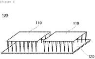
- FIG. 1 is a diagram schematically illustrating a configuration of a customized battery management system (BMS) module 100 according to an exemplary embodiment of the present invention
- FIG. 2 is a diagram illustrating a state in which each of one or more BMS part modules 110 is selected according to different BMS design requests 1 and 2.
- BMS battery management system
- the customized BMS module 100 may generally include one or more BMS part modules 110 and a substrate 120.
- the BMS part module 110 may mean a component (or an element), in which a function-based circuit of the BMS is individually designed and reflected, and for example, various functions, such as a power control function, a measurement function, a temperature sensing function, a booster function, and a DCDC converter function of the BMS, performed in the BMS are separately designed based on each function and are reflected to an element.
- various functions such as a power control function, a measurement function, a temperature sensing function, a booster function, and a DCDC converter function of the BMS, performed in the BMS are separately designed based on each function and are reflected to an element.
- one or more pins which are insertable into pattern recesses provided in the substrate 120, which is to be described below, are provided at one side (for example, a lower side) of the BMS part module 110, and according to the insertion of the pin into the pattern recess, the BMS part module 110 and the substrate 120 are electrically connected with each other and are electrically conducted.
- the plurality of BMS part modules 110 is also formed so as to correspond to the various functions, and when the plurality of BMS part modules 110 may be designed first, and then may be selectively determined so as to correspond to a separate BMS design request, which will be described with reference to FIG. 2 .
- the BMS performs various functions, such as a power control function, a measurement function, a temperature sensing function, a booster function, and a DCDC converter function, and it can be seen that the plurality of BMS part modules 110 is also designed so as to correspond to various functions.
- the BMS part module corresponding to the power control function, the BMS part module corresponding to the booster function, and the BMS part modules performing other functions may be selected and determined
- the BMS part module corresponding to the measurement function, the BMS part module corresponding to the DCDC converter function, and the BMS part modules performing other functions may be selected and determined.
- the different BMS part modules 110 may be selectively disposed and mounted on the different substrates 120, respectively, based on the BMS design request, so that it is possible to standardize a component, it is possible to save development time taken according to verification by a development of a new circuit, and it is not necessary to design a new BMS circuit every time which prevents an increase in cost.
- the substrate 120 means a region, in which the one or more BMS part modules 110 are disposed and mounted, and for example, a substrate, such as a printed circuit board (PCB), a flexible PCB (FPCB), or a breadboard, may be applied.
- a substrate such as a printed circuit board (PCB), a flexible PCB (FPCB), or a breadboard, may be applied.
- the patterned pattern recesses maybe formed at an upper side of the substrate 120, and the pins provided to the BMS part module 110 may be inserted into and mounted to the pattern recesses.
- the pattern recess of the substrate 120 does not have a specific form, but is simply arranged in a repeated pattern, so that the disposition position of the BMS part module 110 may be freely adjusted.
- FIG. 3 is a flowchart illustrating a method of designing the customized BMS module 100 illustrated in FIG. 1 in order.
- a function-based circuit of the BMS is individually designed and reflected to one or more BMS part modules 110 (S301).
- the plurality of BMS part modules 110 may be designed.
- one or more BMS part modules 110 are selectively determined so as to correspond to different BMS design requests and are disposed and mounted onto the substrates 120, respectively (S302).
- the pins provided in each BMS part module 110 are inserted to the upper side of the substrate 120, so that the BMS part module 110 and the substrate 120 are electrically connected and conducted.
- the function-based circuits of the BMS performing various functions are separated, and then are designed and reflected based on each element, and are selectively mounted according to different BMS design requests, so that it is possible to achieve standardization of a component without differently designing the BMS every time in accordance with different component specification, and it is possible to decrease prime cost, decrease verification cost consumed due to a development of a new circuit, and decrease development time.
Landscapes
- Engineering & Computer Science (AREA)
- Manufacturing & Machinery (AREA)
- Microelectronics & Electronic Packaging (AREA)
- Chemical & Material Sciences (AREA)
- Chemical Kinetics & Catalysis (AREA)
- Electrochemistry (AREA)
- General Chemical & Material Sciences (AREA)
- Power Engineering (AREA)
- Physics & Mathematics (AREA)
- General Physics & Mathematics (AREA)
- Battery Mounting, Suspending (AREA)
- Structure Of Printed Boards (AREA)
- Charge And Discharge Circuits For Batteries Or The Like (AREA)
- Secondary Cells (AREA)
Abstract
Description
- This application claims priority to and the benefit of Korean Patent Application No.
10-2017-0104786 - The present invention relates to a customized battery management system (BMS) module and a design method therefor, and more particularly, to a customized BMS module, in which a BMS is separated into parts based on a function and is designed in advance, and a BMS part is selected and is mounted on a substrate so as to correspond to a separate BMS design request, without differently designing the BMS in accordance with different component specifications every time, so that it is possible to achieve standardization of the component and to decrease prime cost, verification cost consumed due to a development of a new circuit, and a development time, and a design method therefor.
- In general, a battery, that is, a secondary battery, used in an electric vehicle (EV), a hybrid vehicle (HV), and for family use or an industry use has high easiness of application according to a product group and has an electric characteristic, such as high energy density, and the like.
- The secondary battery attracts attention as a new energy source for improving environment-friendly and energy efficiency in that it is possible to innovatively decrease use of fossil energy, which is the primary advantage, and a by-product according to the use of energy is not generated at all.
- In this case, when each of the plurality of secondary batteries is alternately charged and discharged, it is necessary to manage the plurality of secondary batteries by efficiently controlling the charging/discharging so that the battery maintains an appropriate operation state and performance, and to this end, a state and performance of the battery are managed by using a battery management system (BMS), and the BMS serves to measure a current, a voltage, a temperature, and the like of the battery, estimate a state of charging (SOC) of the battery based on the measured current, voltage, temperature, and the like, and control an SOC so as to obtain best fuel consumption efficiency.
- In the meantime, in the related art, a specification of a component required for each operation task is different, so that it is necessary to differently design the BMS every time when components and a circuit diagram are designed at the time of development of the BMS, which is an obstacle in achieving the standardization of the component, and is actually a reason causing problems, such as an increase in component cost, an increase in verification cost consumed due to a development of a new circuit, and an increase in development time.
- In this respect, in order to solve various problems and limits generated in the BMS design and development process in the related art, the present inventors developed a customized BMS module, in which a BMS is separated into parts based on a function and is designed in advance, and a BMS part is selected and is mounted on a substrate so as to correspond to a separate BMS design request, without differently designing the BMS in accordance with different component specifications every time, so that it is possible to achieve standardization of the component and to decrease prime cost, verification cost consumed due to a development of a new circuit, and a development time, and a design method therefor.
- The present invention is conceived to solve the foregoing problems, and provides a customized battery management system (BMS) module, in which a BMS is separated into parts based on a function and is designed in advance, and a BMS part is selected and is mounted on a substrate so as to correspond to a separate BMS design request, without differently designing the BMS in accordance with different component specifications every time, so that it is possible to achieve standardization of the component and to decrease prime cost, verification cost consumed due to a development of a new circuit, and a development time, and a design method therefor.
- An exemplary embodiment of the present invention provides a customized battery management system (BMS) module, including: one or more BMS part modules, in which function-based circuits of a BMS are individually designed and reflected; and a substrate, on which the one or more BMS part modules are disposed and mounted, in which the one or more BMS part modules are selectively determined so as to correspond to a separate BMS design request and are disposed and mounted onto the substrate.
- In the exemplary embodiment, circuits based on a power control function, a measurement function, a temperature sensing function, a booster function, and a DCDC converter function of the BMS may be individually designed and reflected to the one or more BMS part modules.
- In the exemplary embodiment, one or more pins inserted into the substrate may be provided in each of the one or more BMS part modules.
- In the exemplary embodiment, in the BMS design request, a list of selectable BMS part modules among the one or more BMS part modules may be pre-organized.
- In the exemplary embodiment, the substrate may be a printed circuit board (PCB), a flexible PCB (FPCB), or a breadboard.
- According to another exemplary embodiment of the present invention provides a method of designing a customized battery management system (BMS) module, the method including: individually designing and reflecting function-based circuits of a BMS to one or more BMS part modules; and selectively determining the one or more BMS part modules so as to correspond to a separate BMS design request and disposing and mounting the determined BMS part modules on a substrate.
- According to one aspect of the present invention, a BMS is separated into parts based on a function and is designed in advance, and a BMS part is selected and is mounted on a substrate so as to correspond to a separate BMS design request, without differently designing the BMS in accordance with different component specifications every time, so that it is possible to achieve standardization of the component and to decrease prime cost, verification cost consumed due to a development of a new circuit, and a development time.
-
-
FIG. 1 is a diagram schematically illustrating a configuration of a customized battery management system (BMS)module 100 according to an exemplary embodiment of the present invention. -
FIG. 2 is a diagram illustrating a state in which each of one or moreBMS part modules 110 is selected according to differentBMS design requests -
FIG. 3 is a flowchart illustrating a method of designing the customizedBMS module 100 illustrated inFIG. 1 in order. - Hereinafter, an exemplary embodiment is presented for help understanding of the present invention. However, the exemplary embodiment below is simply provided for easier understanding of the present invention, and the contents of the present invention are not limited by the exemplary embodiment.
-
FIG. 1 is a diagram schematically illustrating a configuration of a customized battery management system (BMS)module 100 according to an exemplary embodiment of the present invention, andFIG. 2 is a diagram illustrating a state in which each of one or moreBMS part modules 110 is selected according to differentBMS design requests - Referring to
FIGS. 1 and2 , the customizedBMS module 100 according to an exemplary embodiment of the present invention may generally include one or moreBMS part modules 110 and asubstrate 120. - First, the
BMS part module 110 may mean a component (or an element), in which a function-based circuit of the BMS is individually designed and reflected, and for example, various functions, such as a power control function, a measurement function, a temperature sensing function, a booster function, and a DCDC converter function of the BMS, performed in the BMS are separately designed based on each function and are reflected to an element. - In this case, one or more pins, which are insertable into pattern recesses provided in the
substrate 120, which is to be described below, are provided at one side (for example, a lower side) of theBMS part module 110, and according to the insertion of the pin into the pattern recess, theBMS part module 110 and thesubstrate 120 are electrically connected with each other and are electrically conducted. - In the meantime, in the BMS, various functions may be performed as described above, and the plurality of
BMS part modules 110 is also formed so as to correspond to the various functions, and when the plurality ofBMS part modules 110 may be designed first, and then may be selectively determined so as to correspond to a separate BMS design request, which will be described with reference toFIG. 2 . - Referring to
FIG. 2 , the BMS performs various functions, such as a power control function, a measurement function, a temperature sensing function, a booster function, and a DCDC converter function, and it can be seen that the plurality ofBMS part modules 110 is also designed so as to correspond to various functions. - Particularly, for the first BMS design request (for example, a component specification demanded by user A), the BMS part module corresponding to the power control function, the BMS part module corresponding to the booster function, and the BMS part modules performing other functions may be selected and determined, and for the second BMS design request (for example, a component specification demanded by user B), the BMS part module corresponding to the measurement function, the BMS part module corresponding to the DCDC converter function, and the BMS part modules performing other functions may be selected and determined.
- That is, the different
BMS part modules 110 may be selectively disposed and mounted on thedifferent substrates 120, respectively, based on the BMS design request, so that it is possible to standardize a component, it is possible to save development time taken according to verification by a development of a new circuit, and it is not necessary to design a new BMS circuit every time which prevents an increase in cost. - Next, the
substrate 120 means a region, in which the one or moreBMS part modules 110 are disposed and mounted, and for example, a substrate, such as a printed circuit board (PCB), a flexible PCB (FPCB), or a breadboard, may be applied. - In this case, the patterned pattern recesses maybe formed at an upper side of the
substrate 120, and the pins provided to theBMS part module 110 may be inserted into and mounted to the pattern recesses. - Particularly, the pattern recess of the
substrate 120 does not have a specific form, but is simply arranged in a repeated pattern, so that the disposition position of theBMS part module 110 may be freely adjusted. - Next, a process of designing the customized
BMS module 110 will be sequentially described with reference toFIG. 3 . -
FIG. 3 is a flowchart illustrating a method of designing the customizedBMS module 100 illustrated inFIG. 1 in order. - Referring to
FIG. 3 , first, a function-based circuit of the BMS is individually designed and reflected to one or more BMS part modules 110 (S301). In this process, in order to correspond to various functions performed by the BMS, the plurality ofBMS part modules 110 may be designed. - Next, one or more
BMS part modules 110 are selectively determined so as to correspond to different BMS design requests and are disposed and mounted onto thesubstrates 120, respectively (S302). In this case, the pins provided in eachBMS part module 110 are inserted to the upper side of thesubstrate 120, so that theBMS part module 110 and thesubstrate 120 are electrically connected and conducted. - As described above, according to the present invention, the function-based circuits of the BMS performing various functions are separated, and then are designed and reflected based on each element, and are selectively mounted according to different BMS design requests, so that it is possible to achieve standardization of a component without differently designing the BMS every time in accordance with different component specification, and it is possible to decrease prime cost, decrease verification cost consumed due to a development of a new circuit, and decrease development time.
- In the forgoing, the present invention has been described with reference to the exemplary embodiment of the present invention, but those skilled in the art may appreciate that the present invention may be variously corrected and changed within the range without departing from the spirit and the area of the present invention described in the appending claims.
Claims (10)
- A customized battery management system (BMS) module, comprising:one or more BMS part modules, in which function-based circuits of a BMS are individually designed and reflected; anda substrate, on which the one or more BMS part modules are disposed and mounted,wherein the one or more BMS part modules are selectively determined so as to correspond to a separate BMS design request and are disposed and mounted onto the substrate.
- The customized BMS module of claim 1, wherein circuits based on a power control function, a measurement function, a temperature sensing function, a booster function, and a DCDC converter function of the BMS are individually designed and reflected to the one or more BMS part modules.
- The customized BMS module of claim 1, wherein one or more pins inserted into the substrate are provided in each of the one or more BMS part modules.
- The customized BMS module of claim 1, wherein in the BMS design request, a list of selectable BMS part modules among the one or more BMS part modules is pre-organized.
- The customized BMS module of claim 1, wherein the substrate is a printed circuit board (PCB), a flexible PCB (FPCB), or a breadboard.
- A method of designing a customized battery management system (BMS) module, the method comprising:individually designing and reflecting function-based circuits of a BMS to one or more BMS part modules; andselectively determining the one or more BMS part modules so as to correspond to a separate BMS design request and disposing and mounting the determined BMS part modules on a substrate.
- The method of claim 6, wherein circuits based on a power control function, a measurement function, a temperature sensing function, a booster function, and a DCDC converter function of the BMS are individually designed and reflected to the one or more BMS part modules.
- The method of claim 6, wherein one or more pins inserted into the substrate are provided in each of the one or more BMS part modules.
- The method of claim 6, wherein in the BMS design request, a list of selectable BMS part modules among the one or more BMS part modules is pre-organized.
- The method of claim 6, wherein the substrate is a printed circuit board (PCB), a flexible PCB (FPCB), or a breadboard.
Applications Claiming Priority (2)
| Application Number | Priority Date | Filing Date | Title |
|---|---|---|---|
| KR1020170104786A KR102201566B1 (en) | 2017-08-18 | 2017-08-18 | Customized bms module and method for designing thereof |
| PCT/KR2018/009067 WO2019035596A1 (en) | 2017-08-18 | 2018-08-09 | Customized bms module and design method therefor |
Publications (3)
| Publication Number | Publication Date |
|---|---|
| EP3582317A1 true EP3582317A1 (en) | 2019-12-18 |
| EP3582317A4 EP3582317A4 (en) | 2020-05-13 |
| EP3582317B1 EP3582317B1 (en) | 2024-04-17 |
Family
ID=65362699
Family Applications (1)
| Application Number | Title | Priority Date | Filing Date |
|---|---|---|---|
| EP18845679.2A Active EP3582317B1 (en) | 2017-08-18 | 2018-08-09 | Customized bms module and design method therefor |
Country Status (9)
| Country | Link |
|---|---|
| US (1) | US20190393561A1 (en) |
| EP (1) | EP3582317B1 (en) |
| JP (1) | JP7318932B2 (en) |
| KR (1) | KR102201566B1 (en) |
| CN (1) | CN110447144A (en) |
| ES (1) | ES2985077T3 (en) |
| HU (1) | HUE066381T2 (en) |
| PL (1) | PL3582317T3 (en) |
| WO (1) | WO2019035596A1 (en) |
Family Cites Families (33)
| Publication number | Priority date | Publication date | Assignee | Title |
|---|---|---|---|---|
| JP2702707B2 (en) * | 1986-09-30 | 1998-01-26 | ロ−ム株式会社 | Method of manufacturing target chip for 1-chip microcomputer |
| US4922432A (en) * | 1988-01-13 | 1990-05-01 | International Chip Corporation | Knowledge based method and apparatus for designing integrated circuits using functional specifications |
| JPH04127377A (en) * | 1990-09-19 | 1992-04-28 | Ibiden Co Ltd | Designing method for printed circuit board |
| JPH06325126A (en) * | 1993-05-12 | 1994-11-25 | Hitachi Ltd | Printed circuit board CAD system |
| JP3209861B2 (en) * | 1994-09-01 | 2001-09-17 | 沖電気工業株式会社 | Integrated circuit design method |
| JP3718008B2 (en) * | 1996-02-26 | 2005-11-16 | 株式会社日立製作所 | Memory module and manufacturing method thereof |
| JPH09259154A (en) * | 1996-03-19 | 1997-10-03 | Fujitsu Ltd | Logic designing method and device, and semiconductor integrated circuit manufacturing method |
| JP2005175505A (en) * | 1997-08-21 | 2005-06-30 | Renesas Technology Corp | Semiconductor integrated circuit device |
| US6338158B1 (en) * | 1997-10-31 | 2002-01-08 | Vlsi Technology, Inc. | Custom IC hardware modeling using standard ICs for use in IC design validation |
| TW392307B (en) * | 1998-01-13 | 2000-06-01 | Mitsubishi Electric Corp | A method of the manufacture and the setup of the semiconductor apparatus |
| JPH11258267A (en) * | 1998-03-10 | 1999-09-24 | Yokoo Kaikei System Kk | Connector pin unit for breadboard |
| US7024637B2 (en) * | 2003-09-29 | 2006-04-04 | Lsi Logic Corporation | Functionality based package design for integrated circuit blocks |
| US7114134B2 (en) * | 2004-05-27 | 2006-09-26 | Veri Silicon Holdings, Co. Ltd | Automatic circuit design method with a cell library providing transistor size information |
| TWI321841B (en) * | 2005-04-29 | 2010-03-11 | Taiwan Semiconductor Mfg | System on chip development with reconfigurable multi-project wafer technology |
| US7877720B2 (en) * | 2007-01-08 | 2011-01-25 | International Business Machines Corporation | Method and tool for designing electronic circuits on a printed circuit board |
| EP1950096B1 (en) * | 2007-01-24 | 2009-07-15 | Delphi Technologies, Inc. | Modular system |
| KR20090120867A (en) * | 2008-05-21 | 2009-11-25 | 구언두 | Surface Mount LED General Purpose Board |
| US8055217B2 (en) * | 2008-08-05 | 2011-11-08 | Texas Instruments Incorporated | Adaptive complex gain predistorter for a transmitter |
| KR101104667B1 (en) * | 2009-02-26 | 2012-01-13 | 에스케이이노베이션 주식회사 | Battery management system and slave battery management module of the battery management system |
| CN201758090U (en) * | 2010-07-15 | 2011-03-09 | 新巨企业股份有限公司 | Combined keyboard module |
| EP2662922B1 (en) | 2011-03-10 | 2017-11-15 | LG Chem, Ltd. | Battery pack provided with stable measurement means |
| SE535818C2 (en) * | 2011-05-26 | 2013-01-02 | Stanley Wissmar | A mobile wristwatch comprising several electrical and micromechanical components that act as a central unit for a variety of tasks |
| KR101765942B1 (en) * | 2011-08-01 | 2017-08-07 | 엘지이노텍 주식회사 | Tuner module |
| KR20130125906A (en) * | 2012-05-10 | 2013-11-20 | 에스케이이노베이션 주식회사 | Battery management device |
| KR101416799B1 (en) * | 2012-11-27 | 2014-08-06 | 에스케이씨앤씨 주식회사 | Battery management system for integrating master unit and slave unit of |
| JP5686789B2 (en) * | 2012-12-19 | 2015-03-18 | オムロンオートモーティブエレクトロニクス株式会社 | Battery management system, integrated battery management device |
| KR101591150B1 (en) * | 2013-10-31 | 2016-02-02 | 주식회사 엘지화학 | Application module control and hardware call apparatus for standardization of battery |
| US9647471B2 (en) | 2014-10-17 | 2017-05-09 | Trion Energy Solutions Corp. | Battery management system and method |
| CN204066731U (en) * | 2014-09-26 | 2014-12-31 | 惠州市德赛西威汽车电子有限公司 | A kind of divergence type vehicle entertainment system |
| KR101750488B1 (en) * | 2014-11-24 | 2017-06-23 | 주식회사 엘지화학 | Abnormal-temperature Sensing Assembly Comprising Series-connected PTC Thermistors and Battery Pack Comprising the Same |
| KR101726930B1 (en) * | 2014-12-08 | 2017-04-13 | 주식회사 엘지화학 | Communication system and connecting method for communicating between battery management systems |
| CN106155186A (en) * | 2015-04-02 | 2016-11-23 | 深圳市兴华盛科技有限公司 | A kind of embedded main board and electronic product thereof |
| KR101818596B1 (en) | 2016-03-08 | 2018-02-21 | 이엔컴퍼지트 주식회사 | Reinforced panel forming apparatus |
-
2017
- 2017-08-18 KR KR1020170104786A patent/KR102201566B1/en active Active
-
2018
- 2018-08-09 ES ES18845679T patent/ES2985077T3/en active Active
- 2018-08-09 WO PCT/KR2018/009067 patent/WO2019035596A1/en not_active Ceased
- 2018-08-09 PL PL18845679.2T patent/PL3582317T3/en unknown
- 2018-08-09 EP EP18845679.2A patent/EP3582317B1/en active Active
- 2018-08-09 JP JP2019545338A patent/JP7318932B2/en active Active
- 2018-08-09 US US16/489,250 patent/US20190393561A1/en not_active Abandoned
- 2018-08-09 CN CN201880019513.3A patent/CN110447144A/en active Pending
- 2018-08-09 HU HUE18845679A patent/HUE066381T2/en unknown
Also Published As
| Publication number | Publication date |
|---|---|
| KR20190019614A (en) | 2019-02-27 |
| EP3582317B1 (en) | 2024-04-17 |
| PL3582317T3 (en) | 2024-06-10 |
| JP2020510389A (en) | 2020-04-02 |
| ES2985077T3 (en) | 2024-11-04 |
| CN110447144A (en) | 2019-11-12 |
| EP3582317A4 (en) | 2020-05-13 |
| JP7318932B2 (en) | 2023-08-01 |
| HUE066381T2 (en) | 2024-08-28 |
| WO2019035596A1 (en) | 2019-02-21 |
| KR102201566B1 (en) | 2021-01-11 |
| US20190393561A1 (en) | 2019-12-26 |
Similar Documents
| Publication | Publication Date | Title |
|---|---|---|
| US11247582B2 (en) | Control electronics for a battery system, method for power supplying control electronics for a battery system, battery system and vehicle | |
| KR102530002B1 (en) | Control electronics for battery system, method for power supplying control electronics for battery system, battery system and vehicle | |
| CN109906168B (en) | Management device for battery pack | |
| EP2963767B1 (en) | System and method for allocating communication identifier for multi-bms | |
| KR100906907B1 (en) | Car battery management system | |
| EP2833503B1 (en) | Charging/discharging control device and charging/discharging control method | |
| US9969296B2 (en) | Battery module, method for manufacturing the same, and electric vehicle using the same | |
| CN101362442B (en) | Electrically powered vehicle | |
| US10050316B2 (en) | Communication between battery cells | |
| CN106463985B (en) | Balance correction control device, balance correction system, and electricity storage system | |
| US20140327407A1 (en) | Method and system for managing the electric charges of battery cells | |
| CN103997071B (en) | Systems and methods for charging multiple vehicle rechargeable energy storage systems | |
| CN106030964B (en) | Battery management unit and method for setting identifier by using frequency modulation | |
| US9153973B2 (en) | Active cell balancing | |
| KR102472234B1 (en) | Method and detection system for determining support of energy content and power of battery | |
| KR102417889B1 (en) | Apparatus for controlling charging of low voltage battery in elcetric vehicle and method thereof | |
| EP3582317B1 (en) | Customized bms module and design method therefor | |
| KR102473145B1 (en) | Battery system with internally powered real time clock and power supply circuit for a real time clock | |
| CN103986203A (en) | Storage battery and method for adjusting storage battery voltage by using quality factors | |
| KR20250052650A (en) | Smart battery system based on reusable batteries | |
| JP6879135B2 (en) | Warm-up system | |
| EP2733009B1 (en) | Vehicle charging system | |
| KR20160034663A (en) | System and method for relaying data communication between modules |
Legal Events
| Date | Code | Title | Description |
|---|---|---|---|
| STAA | Information on the status of an ep patent application or granted ep patent |
Free format text: STATUS: THE INTERNATIONAL PUBLICATION HAS BEEN MADE |
|
| PUAI | Public reference made under article 153(3) epc to a published international application that has entered the european phase |
Free format text: ORIGINAL CODE: 0009012 |
|
| STAA | Information on the status of an ep patent application or granted ep patent |
Free format text: STATUS: REQUEST FOR EXAMINATION WAS MADE |
|
| 17P | Request for examination filed |
Effective date: 20190911 |
|
| AK | Designated contracting states |
Kind code of ref document: A1 Designated state(s): AL AT BE BG CH CY CZ DE DK EE ES FI FR GB GR HR HU IE IS IT LI LT LU LV MC MK MT NL NO PL PT RO RS SE SI SK SM TR |
|
| AX | Request for extension of the european patent |
Extension state: BA ME |
|
| A4 | Supplementary search report drawn up and despatched |
Effective date: 20200414 |
|
| RIC1 | Information provided on ipc code assigned before grant |
Ipc: H05K 13/04 20060101ALI20200406BHEP Ipc: H01M 10/42 20060101AFI20200406BHEP Ipc: H02J 7/00 20060101ALI20200406BHEP |
|
| DAV | Request for validation of the european patent (deleted) | ||
| DAX | Request for extension of the european patent (deleted) | ||
| RAP1 | Party data changed (applicant data changed or rights of an application transferred) |
Owner name: LG ENERGY SOLUTION LTD. |
|
| RAP3 | Party data changed (applicant data changed or rights of an application transferred) |
Owner name: LG ENERGY SOLUTION, LTD. |
|
| STAA | Information on the status of an ep patent application or granted ep patent |
Free format text: STATUS: EXAMINATION IS IN PROGRESS |
|
| 17Q | First examination report despatched |
Effective date: 20230707 |
|
| GRAP | Despatch of communication of intention to grant a patent |
Free format text: ORIGINAL CODE: EPIDOSNIGR1 |
|
| STAA | Information on the status of an ep patent application or granted ep patent |
Free format text: STATUS: GRANT OF PATENT IS INTENDED |
|
| INTG | Intention to grant announced |
Effective date: 20231218 |
|
| GRAS | Grant fee paid |
Free format text: ORIGINAL CODE: EPIDOSNIGR3 |
|
| GRAA | (expected) grant |
Free format text: ORIGINAL CODE: 0009210 |
|
| STAA | Information on the status of an ep patent application or granted ep patent |
Free format text: STATUS: THE PATENT HAS BEEN GRANTED |
|
| P01 | Opt-out of the competence of the unified patent court (upc) registered |
Effective date: 20240305 |
|
| AK | Designated contracting states |
Kind code of ref document: B1 Designated state(s): AL AT BE BG CH CY CZ DE DK EE ES FI FR GB GR HR HU IE IS IT LI LT LU LV MC MK MT NL NO PL PT RO RS SE SI SK SM TR |
|
| REG | Reference to a national code |
Ref country code: GB Ref legal event code: FG4D |
|
| REG | Reference to a national code |
Ref country code: CH Ref legal event code: EP |
|
| REG | Reference to a national code |
Ref country code: DE Ref legal event code: R096 Ref document number: 602018068308 Country of ref document: DE |
|
| REG | Reference to a national code |
Ref country code: IE Ref legal event code: FG4D |
|
| REG | Reference to a national code |
Ref country code: SE Ref legal event code: TRGR |
|
| REG | Reference to a national code |
Ref country code: LT Ref legal event code: MG9D |
|
| REG | Reference to a national code |
Ref country code: NL Ref legal event code: MP Effective date: 20240417 |
|
| REG | Reference to a national code |
Ref country code: HU Ref legal event code: AG4A Ref document number: E066381 Country of ref document: HU |
|
| REG | Reference to a national code |
Ref country code: AT Ref legal event code: MK05 Ref document number: 1678155 Country of ref document: AT Kind code of ref document: T Effective date: 20240417 |
|
| PG25 | Lapsed in a contracting state [announced via postgrant information from national office to epo] |
Ref country code: NL Free format text: LAPSE BECAUSE OF FAILURE TO SUBMIT A TRANSLATION OF THE DESCRIPTION OR TO PAY THE FEE WITHIN THE PRESCRIBED TIME-LIMIT Effective date: 20240417 |
|
| PG25 | Lapsed in a contracting state [announced via postgrant information from national office to epo] |
Ref country code: NL Free format text: LAPSE BECAUSE OF FAILURE TO SUBMIT A TRANSLATION OF THE DESCRIPTION OR TO PAY THE FEE WITHIN THE PRESCRIBED TIME-LIMIT Effective date: 20240417 |
|
| PG25 | Lapsed in a contracting state [announced via postgrant information from national office to epo] |
Ref country code: IS Free format text: LAPSE BECAUSE OF FAILURE TO SUBMIT A TRANSLATION OF THE DESCRIPTION OR TO PAY THE FEE WITHIN THE PRESCRIBED TIME-LIMIT Effective date: 20240817 |
|
| PG25 | Lapsed in a contracting state [announced via postgrant information from national office to epo] |
Ref country code: BG Free format text: LAPSE BECAUSE OF FAILURE TO SUBMIT A TRANSLATION OF THE DESCRIPTION OR TO PAY THE FEE WITHIN THE PRESCRIBED TIME-LIMIT Effective date: 20240417 |
|
| PG25 | Lapsed in a contracting state [announced via postgrant information from national office to epo] |
Ref country code: HR Free format text: LAPSE BECAUSE OF FAILURE TO SUBMIT A TRANSLATION OF THE DESCRIPTION OR TO PAY THE FEE WITHIN THE PRESCRIBED TIME-LIMIT Effective date: 20240417 Ref country code: FI Free format text: LAPSE BECAUSE OF FAILURE TO SUBMIT A TRANSLATION OF THE DESCRIPTION OR TO PAY THE FEE WITHIN THE PRESCRIBED TIME-LIMIT Effective date: 20240417 |
|
| PG25 | Lapsed in a contracting state [announced via postgrant information from national office to epo] |
Ref country code: GR Free format text: LAPSE BECAUSE OF FAILURE TO SUBMIT A TRANSLATION OF THE DESCRIPTION OR TO PAY THE FEE WITHIN THE PRESCRIBED TIME-LIMIT Effective date: 20240718 |
|
| PG25 | Lapsed in a contracting state [announced via postgrant information from national office to epo] |
Ref country code: PT Free format text: LAPSE BECAUSE OF FAILURE TO SUBMIT A TRANSLATION OF THE DESCRIPTION OR TO PAY THE FEE WITHIN THE PRESCRIBED TIME-LIMIT Effective date: 20240819 |
|
| PG25 | Lapsed in a contracting state [announced via postgrant information from national office to epo] |
Ref country code: AT Free format text: LAPSE BECAUSE OF FAILURE TO SUBMIT A TRANSLATION OF THE DESCRIPTION OR TO PAY THE FEE WITHIN THE PRESCRIBED TIME-LIMIT Effective date: 20240417 |
|
| PG25 | Lapsed in a contracting state [announced via postgrant information from national office to epo] |
Ref country code: LV Free format text: LAPSE BECAUSE OF FAILURE TO SUBMIT A TRANSLATION OF THE DESCRIPTION OR TO PAY THE FEE WITHIN THE PRESCRIBED TIME-LIMIT Effective date: 20240417 |
|
| PG25 | Lapsed in a contracting state [announced via postgrant information from national office to epo] |
Ref country code: PT Free format text: LAPSE BECAUSE OF FAILURE TO SUBMIT A TRANSLATION OF THE DESCRIPTION OR TO PAY THE FEE WITHIN THE PRESCRIBED TIME-LIMIT Effective date: 20240819 Ref country code: NO Free format text: LAPSE BECAUSE OF FAILURE TO SUBMIT A TRANSLATION OF THE DESCRIPTION OR TO PAY THE FEE WITHIN THE PRESCRIBED TIME-LIMIT Effective date: 20240717 Ref country code: LV Free format text: LAPSE BECAUSE OF FAILURE TO SUBMIT A TRANSLATION OF THE DESCRIPTION OR TO PAY THE FEE WITHIN THE PRESCRIBED TIME-LIMIT Effective date: 20240417 Ref country code: IS Free format text: LAPSE BECAUSE OF FAILURE TO SUBMIT A TRANSLATION OF THE DESCRIPTION OR TO PAY THE FEE WITHIN THE PRESCRIBED TIME-LIMIT Effective date: 20240817 Ref country code: HR Free format text: LAPSE BECAUSE OF FAILURE TO SUBMIT A TRANSLATION OF THE DESCRIPTION OR TO PAY THE FEE WITHIN THE PRESCRIBED TIME-LIMIT Effective date: 20240417 Ref country code: GR Free format text: LAPSE BECAUSE OF FAILURE TO SUBMIT A TRANSLATION OF THE DESCRIPTION OR TO PAY THE FEE WITHIN THE PRESCRIBED TIME-LIMIT Effective date: 20240718 Ref country code: FI Free format text: LAPSE BECAUSE OF FAILURE TO SUBMIT A TRANSLATION OF THE DESCRIPTION OR TO PAY THE FEE WITHIN THE PRESCRIBED TIME-LIMIT Effective date: 20240417 Ref country code: BG Free format text: LAPSE BECAUSE OF FAILURE TO SUBMIT A TRANSLATION OF THE DESCRIPTION OR TO PAY THE FEE WITHIN THE PRESCRIBED TIME-LIMIT Effective date: 20240417 Ref country code: AT Free format text: LAPSE BECAUSE OF FAILURE TO SUBMIT A TRANSLATION OF THE DESCRIPTION OR TO PAY THE FEE WITHIN THE PRESCRIBED TIME-LIMIT Effective date: 20240417 Ref country code: RS Free format text: LAPSE BECAUSE OF FAILURE TO SUBMIT A TRANSLATION OF THE DESCRIPTION OR TO PAY THE FEE WITHIN THE PRESCRIBED TIME-LIMIT Effective date: 20240717 |
|
| REG | Reference to a national code |
Ref country code: ES Ref legal event code: FG2A Ref document number: 2985077 Country of ref document: ES Kind code of ref document: T3 Effective date: 20241104 |
|
| PG25 | Lapsed in a contracting state [announced via postgrant information from national office to epo] |
Ref country code: DK Free format text: LAPSE BECAUSE OF FAILURE TO SUBMIT A TRANSLATION OF THE DESCRIPTION OR TO PAY THE FEE WITHIN THE PRESCRIBED TIME-LIMIT Effective date: 20240417 |
|
| REG | Reference to a national code |
Ref country code: DE Ref legal event code: R097 Ref document number: 602018068308 Country of ref document: DE |
|
| PG25 | Lapsed in a contracting state [announced via postgrant information from national office to epo] |
Ref country code: EE Free format text: LAPSE BECAUSE OF FAILURE TO SUBMIT A TRANSLATION OF THE DESCRIPTION OR TO PAY THE FEE WITHIN THE PRESCRIBED TIME-LIMIT Effective date: 20240417 |
|
| PG25 | Lapsed in a contracting state [announced via postgrant information from national office to epo] |
Ref country code: CZ Free format text: LAPSE BECAUSE OF FAILURE TO SUBMIT A TRANSLATION OF THE DESCRIPTION OR TO PAY THE FEE WITHIN THE PRESCRIBED TIME-LIMIT Effective date: 20240417 |
|
| PG25 | Lapsed in a contracting state [announced via postgrant information from national office to epo] |
Ref country code: SK Free format text: LAPSE BECAUSE OF FAILURE TO SUBMIT A TRANSLATION OF THE DESCRIPTION OR TO PAY THE FEE WITHIN THE PRESCRIBED TIME-LIMIT Effective date: 20240417 Ref country code: RO Free format text: LAPSE BECAUSE OF FAILURE TO SUBMIT A TRANSLATION OF THE DESCRIPTION OR TO PAY THE FEE WITHIN THE PRESCRIBED TIME-LIMIT Effective date: 20240417 |
|
| PG25 | Lapsed in a contracting state [announced via postgrant information from national office to epo] |
Ref country code: SM Free format text: LAPSE BECAUSE OF FAILURE TO SUBMIT A TRANSLATION OF THE DESCRIPTION OR TO PAY THE FEE WITHIN THE PRESCRIBED TIME-LIMIT Effective date: 20240417 |
|
| PG25 | Lapsed in a contracting state [announced via postgrant information from national office to epo] |
Ref country code: SM Free format text: LAPSE BECAUSE OF FAILURE TO SUBMIT A TRANSLATION OF THE DESCRIPTION OR TO PAY THE FEE WITHIN THE PRESCRIBED TIME-LIMIT Effective date: 20240417 Ref country code: SK Free format text: LAPSE BECAUSE OF FAILURE TO SUBMIT A TRANSLATION OF THE DESCRIPTION OR TO PAY THE FEE WITHIN THE PRESCRIBED TIME-LIMIT Effective date: 20240417 Ref country code: RO Free format text: LAPSE BECAUSE OF FAILURE TO SUBMIT A TRANSLATION OF THE DESCRIPTION OR TO PAY THE FEE WITHIN THE PRESCRIBED TIME-LIMIT Effective date: 20240417 Ref country code: EE Free format text: LAPSE BECAUSE OF FAILURE TO SUBMIT A TRANSLATION OF THE DESCRIPTION OR TO PAY THE FEE WITHIN THE PRESCRIBED TIME-LIMIT Effective date: 20240417 Ref country code: DK Free format text: LAPSE BECAUSE OF FAILURE TO SUBMIT A TRANSLATION OF THE DESCRIPTION OR TO PAY THE FEE WITHIN THE PRESCRIBED TIME-LIMIT Effective date: 20240417 Ref country code: CZ Free format text: LAPSE BECAUSE OF FAILURE TO SUBMIT A TRANSLATION OF THE DESCRIPTION OR TO PAY THE FEE WITHIN THE PRESCRIBED TIME-LIMIT Effective date: 20240417 |
|
| PG25 | Lapsed in a contracting state [announced via postgrant information from national office to epo] |
Ref country code: IT Free format text: LAPSE BECAUSE OF FAILURE TO SUBMIT A TRANSLATION OF THE DESCRIPTION OR TO PAY THE FEE WITHIN THE PRESCRIBED TIME-LIMIT Effective date: 20240417 |
|
| PLBE | No opposition filed within time limit |
Free format text: ORIGINAL CODE: 0009261 |
|
| STAA | Information on the status of an ep patent application or granted ep patent |
Free format text: STATUS: NO OPPOSITION FILED WITHIN TIME LIMIT |
|
| 26N | No opposition filed |
Effective date: 20250120 |
|
| REG | Reference to a national code |
Ref country code: CH Ref legal event code: PL |
|
| PG25 | Lapsed in a contracting state [announced via postgrant information from national office to epo] |
Ref country code: LU Free format text: LAPSE BECAUSE OF NON-PAYMENT OF DUE FEES Effective date: 20240809 |
|
| PG25 | Lapsed in a contracting state [announced via postgrant information from national office to epo] |
Ref country code: SI Free format text: LAPSE BECAUSE OF FAILURE TO SUBMIT A TRANSLATION OF THE DESCRIPTION OR TO PAY THE FEE WITHIN THE PRESCRIBED TIME-LIMIT Effective date: 20240417 Ref country code: MC Free format text: LAPSE BECAUSE OF FAILURE TO SUBMIT A TRANSLATION OF THE DESCRIPTION OR TO PAY THE FEE WITHIN THE PRESCRIBED TIME-LIMIT Effective date: 20240417 Ref country code: CH Free format text: LAPSE BECAUSE OF NON-PAYMENT OF DUE FEES Effective date: 20240831 |
|
| REG | Reference to a national code |
Ref country code: BE Ref legal event code: MM Effective date: 20240831 |
|
| PG25 | Lapsed in a contracting state [announced via postgrant information from national office to epo] |
Ref country code: BE Free format text: LAPSE BECAUSE OF NON-PAYMENT OF DUE FEES Effective date: 20240831 |
|
| PG25 | Lapsed in a contracting state [announced via postgrant information from national office to epo] |
Ref country code: IE Free format text: LAPSE BECAUSE OF NON-PAYMENT OF DUE FEES Effective date: 20240809 |
|
| PGFP | Annual fee paid to national office [announced via postgrant information from national office to epo] |
Ref country code: HU Payment date: 20250827 Year of fee payment: 8 |
|
| PGFP | Annual fee paid to national office [announced via postgrant information from national office to epo] |
Ref country code: ES Payment date: 20250911 Year of fee payment: 8 |
|
| PGFP | Annual fee paid to national office [announced via postgrant information from national office to epo] |
Ref country code: DE Payment date: 20250721 Year of fee payment: 8 |
|
| PGFP | Annual fee paid to national office [announced via postgrant information from national office to epo] |
Ref country code: PL Payment date: 20250723 Year of fee payment: 8 |
|
| PGFP | Annual fee paid to national office [announced via postgrant information from national office to epo] |
Ref country code: GB Payment date: 20250722 Year of fee payment: 8 |
|
| PGFP | Annual fee paid to national office [announced via postgrant information from national office to epo] |
Ref country code: FR Payment date: 20250725 Year of fee payment: 8 |
|
| PGFP | Annual fee paid to national office [announced via postgrant information from national office to epo] |
Ref country code: SE Payment date: 20250722 Year of fee payment: 8 |
|
| PG25 | Lapsed in a contracting state [announced via postgrant information from national office to epo] |
Ref country code: CY Free format text: LAPSE BECAUSE OF FAILURE TO SUBMIT A TRANSLATION OF THE DESCRIPTION OR TO PAY THE FEE WITHIN THE PRESCRIBED TIME-LIMIT; INVALID AB INITIO Effective date: 20180809 |