EP3579668A1 - Partially molded substrate and partial molding device and method - Google Patents
Partially molded substrate and partial molding device and method Download PDFInfo
- Publication number
- EP3579668A1 EP3579668A1 EP18818161.4A EP18818161A EP3579668A1 EP 3579668 A1 EP3579668 A1 EP 3579668A1 EP 18818161 A EP18818161 A EP 18818161A EP 3579668 A1 EP3579668 A1 EP 3579668A1
- Authority
- EP
- European Patent Office
- Prior art keywords
- molding
- conductor
- insulator
- substrate
- conductors
- Prior art date
- Legal status (The legal status is an assumption and is not a legal conclusion. Google has not performed a legal analysis and makes no representation as to the accuracy of the status listed.)
- Pending
Links
Images


Classifications
-
- H—ELECTRICITY
- H05—ELECTRIC TECHNIQUES NOT OTHERWISE PROVIDED FOR
- H05K—PRINTED CIRCUITS; CASINGS OR CONSTRUCTIONAL DETAILS OF ELECTRIC APPARATUS; MANUFACTURE OF ASSEMBLAGES OF ELECTRICAL COMPONENTS
- H05K1/00—Printed circuits
- H05K1/02—Details
- H05K1/03—Use of materials for the substrate
- H05K1/05—Insulated conductive substrates, e.g. insulated metal substrate
- H05K1/056—Insulated conductive substrates, e.g. insulated metal substrate the metal substrate being covered by an organic insulating layer
-
- H—ELECTRICITY
- H05—ELECTRIC TECHNIQUES NOT OTHERWISE PROVIDED FOR
- H05K—PRINTED CIRCUITS; CASINGS OR CONSTRUCTIONAL DETAILS OF ELECTRIC APPARATUS; MANUFACTURE OF ASSEMBLAGES OF ELECTRICAL COMPONENTS
- H05K1/00—Printed circuits
- H05K1/02—Details
- H05K1/0213—Electrical arrangements not otherwise provided for
- H05K1/0254—High voltage adaptations; Electrical insulation details; Overvoltage or electrostatic discharge protection ; Arrangements for regulating voltages or for using plural voltages
- H05K1/0256—Electrical insulation details, e.g. around high voltage areas
-
- B—PERFORMING OPERATIONS; TRANSPORTING
- B29—WORKING OF PLASTICS; WORKING OF SUBSTANCES IN A PLASTIC STATE IN GENERAL
- B29C—SHAPING OR JOINING OF PLASTICS; SHAPING OF MATERIAL IN A PLASTIC STATE, NOT OTHERWISE PROVIDED FOR; AFTER-TREATMENT OF THE SHAPED PRODUCTS, e.g. REPAIRING
- B29C37/00—Component parts, details, accessories or auxiliary operations, not covered by group B29C33/00 or B29C35/00
-
- B—PERFORMING OPERATIONS; TRANSPORTING
- B29—WORKING OF PLASTICS; WORKING OF SUBSTANCES IN A PLASTIC STATE IN GENERAL
- B29C—SHAPING OR JOINING OF PLASTICS; SHAPING OF MATERIAL IN A PLASTIC STATE, NOT OTHERWISE PROVIDED FOR; AFTER-TREATMENT OF THE SHAPED PRODUCTS, e.g. REPAIRING
- B29C70/00—Shaping composites, i.e. plastics material comprising reinforcements, fillers or preformed parts, e.g. inserts
- B29C70/68—Shaping composites, i.e. plastics material comprising reinforcements, fillers or preformed parts, e.g. inserts by incorporating or moulding on preformed parts, e.g. inserts or layers, e.g. foam blocks
- B29C70/681—Component parts, details or accessories; Auxiliary operations
-
- B—PERFORMING OPERATIONS; TRANSPORTING
- B29—WORKING OF PLASTICS; WORKING OF SUBSTANCES IN A PLASTIC STATE IN GENERAL
- B29C—SHAPING OR JOINING OF PLASTICS; SHAPING OF MATERIAL IN A PLASTIC STATE, NOT OTHERWISE PROVIDED FOR; AFTER-TREATMENT OF THE SHAPED PRODUCTS, e.g. REPAIRING
- B29C70/00—Shaping composites, i.e. plastics material comprising reinforcements, fillers or preformed parts, e.g. inserts
- B29C70/68—Shaping composites, i.e. plastics material comprising reinforcements, fillers or preformed parts, e.g. inserts by incorporating or moulding on preformed parts, e.g. inserts or layers, e.g. foam blocks
- B29C70/74—Moulding material on a relatively small portion of the preformed part, e.g. outsert moulding
-
- B—PERFORMING OPERATIONS; TRANSPORTING
- B29—WORKING OF PLASTICS; WORKING OF SUBSTANCES IN A PLASTIC STATE IN GENERAL
- B29C—SHAPING OR JOINING OF PLASTICS; SHAPING OF MATERIAL IN A PLASTIC STATE, NOT OTHERWISE PROVIDED FOR; AFTER-TREATMENT OF THE SHAPED PRODUCTS, e.g. REPAIRING
- B29C70/00—Shaping composites, i.e. plastics material comprising reinforcements, fillers or preformed parts, e.g. inserts
- B29C70/88—Shaping composites, i.e. plastics material comprising reinforcements, fillers or preformed parts, e.g. inserts characterised primarily by possessing specific properties, e.g. electrically conductive or locally reinforced
- B29C70/882—Shaping composites, i.e. plastics material comprising reinforcements, fillers or preformed parts, e.g. inserts characterised primarily by possessing specific properties, e.g. electrically conductive or locally reinforced partly or totally electrically conductive, e.g. for EMI shielding
-
- H—ELECTRICITY
- H05—ELECTRIC TECHNIQUES NOT OTHERWISE PROVIDED FOR
- H05K—PRINTED CIRCUITS; CASINGS OR CONSTRUCTIONAL DETAILS OF ELECTRIC APPARATUS; MANUFACTURE OF ASSEMBLAGES OF ELECTRICAL COMPONENTS
- H05K1/00—Printed circuits
- H05K1/02—Details
- H05K1/0213—Electrical arrangements not otherwise provided for
- H05K1/0216—Reduction of cross-talk, noise or electromagnetic interference
-
- H—ELECTRICITY
- H05—ELECTRIC TECHNIQUES NOT OTHERWISE PROVIDED FOR
- H05K—PRINTED CIRCUITS; CASINGS OR CONSTRUCTIONAL DETAILS OF ELECTRIC APPARATUS; MANUFACTURE OF ASSEMBLAGES OF ELECTRICAL COMPONENTS
- H05K3/00—Apparatus or processes for manufacturing printed circuits
- H05K3/0091—Apparatus for coating printed circuits using liquid non-metallic coating compositions
-
- H—ELECTRICITY
- H05—ELECTRIC TECHNIQUES NOT OTHERWISE PROVIDED FOR
- H05K—PRINTED CIRCUITS; CASINGS OR CONSTRUCTIONAL DETAILS OF ELECTRIC APPARATUS; MANUFACTURE OF ASSEMBLAGES OF ELECTRICAL COMPONENTS
- H05K3/00—Apparatus or processes for manufacturing printed circuits
- H05K3/22—Secondary treatment of printed circuits
- H05K3/28—Applying non-metallic protective coatings
-
- B—PERFORMING OPERATIONS; TRANSPORTING
- B29—WORKING OF PLASTICS; WORKING OF SUBSTANCES IN A PLASTIC STATE IN GENERAL
- B29C—SHAPING OR JOINING OF PLASTICS; SHAPING OF MATERIAL IN A PLASTIC STATE, NOT OTHERWISE PROVIDED FOR; AFTER-TREATMENT OF THE SHAPED PRODUCTS, e.g. REPAIRING
- B29C37/00—Component parts, details, accessories or auxiliary operations, not covered by group B29C33/00 or B29C35/00
- B29C2037/90—Measuring, controlling or regulating
-
- B—PERFORMING OPERATIONS; TRANSPORTING
- B29—WORKING OF PLASTICS; WORKING OF SUBSTANCES IN A PLASTIC STATE IN GENERAL
- B29L—INDEXING SCHEME ASSOCIATED WITH SUBCLASS B29C, RELATING TO PARTICULAR ARTICLES
- B29L2031/00—Other particular articles
- B29L2031/34—Electrical apparatus, e.g. sparking plugs or parts thereof
- B29L2031/3425—Printed circuits
-
- H—ELECTRICITY
- H05—ELECTRIC TECHNIQUES NOT OTHERWISE PROVIDED FOR
- H05K—PRINTED CIRCUITS; CASINGS OR CONSTRUCTIONAL DETAILS OF ELECTRIC APPARATUS; MANUFACTURE OF ASSEMBLAGES OF ELECTRICAL COMPONENTS
- H05K2201/00—Indexing scheme relating to printed circuits covered by H05K1/00
- H05K2201/01—Dielectrics
- H05K2201/0137—Materials
- H05K2201/0162—Silicon containing polymer, e.g. silicone
-
- H—ELECTRICITY
- H05—ELECTRIC TECHNIQUES NOT OTHERWISE PROVIDED FOR
- H05K—PRINTED CIRCUITS; CASINGS OR CONSTRUCTIONAL DETAILS OF ELECTRIC APPARATUS; MANUFACTURE OF ASSEMBLAGES OF ELECTRICAL COMPONENTS
- H05K2201/00—Indexing scheme relating to printed circuits covered by H05K1/00
- H05K2201/09—Shape and layout
- H05K2201/09818—Shape or layout details not covered by a single group of H05K2201/09009 - H05K2201/09809
- H05K2201/0989—Coating free areas, e.g. areas other than pads or lands free of solder resist
-
- H—ELECTRICITY
- H05—ELECTRIC TECHNIQUES NOT OTHERWISE PROVIDED FOR
- H05K—PRINTED CIRCUITS; CASINGS OR CONSTRUCTIONAL DETAILS OF ELECTRIC APPARATUS; MANUFACTURE OF ASSEMBLAGES OF ELECTRICAL COMPONENTS
- H05K2203/00—Indexing scheme relating to apparatus or processes for manufacturing printed circuits covered by H05K3/00
- H05K2203/13—Moulding and encapsulation; Deposition techniques; Protective layers
- H05K2203/1305—Moulding and encapsulation
- H05K2203/1327—Moulding over PCB locally or completely
-
- H—ELECTRICITY
- H05—ELECTRIC TECHNIQUES NOT OTHERWISE PROVIDED FOR
- H05K—PRINTED CIRCUITS; CASINGS OR CONSTRUCTIONAL DETAILS OF ELECTRIC APPARATUS; MANUFACTURE OF ASSEMBLAGES OF ELECTRICAL COMPONENTS
- H05K2203/00—Indexing scheme relating to apparatus or processes for manufacturing printed circuits covered by H05K3/00
- H05K2203/16—Inspection; Monitoring; Aligning
- H05K2203/163—Monitoring a manufacturing process
-
- H—ELECTRICITY
- H05—ELECTRIC TECHNIQUES NOT OTHERWISE PROVIDED FOR
- H05K—PRINTED CIRCUITS; CASINGS OR CONSTRUCTIONAL DETAILS OF ELECTRIC APPARATUS; MANUFACTURE OF ASSEMBLAGES OF ELECTRICAL COMPONENTS
- H05K3/00—Apparatus or processes for manufacturing printed circuits
- H05K3/22—Secondary treatment of printed circuits
- H05K3/28—Applying non-metallic protective coatings
- H05K3/285—Permanent coating compositions
Definitions
- the present invention relates to a partially molded substrate and a partial molding apparatus and a method thereof, and more particularly, to a partially molded substrate and a partial molding apparatus and a method thereof, which cover and mold each of one or more conductors formed on a substrate with an insulator to prevent a size of the substrate from being increased due to molding, efficiently prevent high voltage from being applied between the conductors on the substrate, and prevent interference around the conductor.
- PCB substrate In general, when a printed circuit board (PCB) substrate is designed, in order to prevent voltage interference between conductors on a substrate, the PCB substrate needs to be designed by maintaining an isolation distance including a clearance distance and a creepage distance between the conductors.
- PCB printed circuit board
- An object of the present invention is to provide a partially molded substrate and a partial molding apparatus and a method thereof, which cover and mold each of one or more conductors formed on a substrate with an insulator to prevent the size of the substrate from being unnecessarily increased due to molding.
- an object of the present invention is to provide a partially molded substrate and a partial molding apparatus and a method thereof, which cover and mold each of one or more conductors formed on a substrate with the insulator to efficiently prevent voltage between the conductors on the substrate from being applied, and prevent interference around the conductor.
- an object of the present invention is to provide a partially molded substrate and a partial molding apparatus and a method thereof, which mold each of one or more conductors formed on a substrate to prevent a part on a PCB substrate including the conductor from being unnecessarily buried in the molding.
- an object of the present invention is to provide a partially molded substrate and a partial molding apparatus and a method thereof, which selectively mold any one or more conductors which need to be molded among one or more conductors formed on a substrate to efficiently use the insulator.
- an object of the present invention is to provide a partially molded substrate and a partial molding apparatus and a method thereof, which efficiently use the insulator by selectively molding one or more conductors formed on a substrate to reduce design cost of the PCB substrate.
- an object of the present invention is to provide a partially molded substrate and a partial molding apparatus and a method thereof, which selectively mold one or more conductors formed on a substrate by setting a molding thickness of an insulator to prevent a thickness of the PCB substrate from being unnecessarily increased due to the molding.
- a partially molded substrate according to an embodiment of the present invention may include one or more conductors formed on one surface, and each of one or more conductors may be covered and molded with an insulator.
- the protruding conductor in the partially molded substrate, may be covered and molded with an insulation cap formed by the insulator.
- the conductor in the partially molded substrate, may be covered and molded with the insulator having a predetermined thickness.
- the conductor positioned in a predetermined molding region may be covered and molded with the insulator.
- the conductor to which voltage equal to or higher than predetermined voltage is applied among one or more conductors is applied may be covered and molded with the insulator.
- a partial molding apparatus may include: a substrate; one or more conductors formed on one surface of the substrate; a sensing unit sensing one or more conductors; and a molding unit covering and molding each of one or more conductors sensed by the sensing unit with the insulator.
- the molding unit when the conductor protrudes, may cover and mold the protruding conductor with an insulation cap formed by the insulator.
- the molding unit when a molding thickness is set, the molding unit may cover and mold the conductor with the insulator in the set thickness.
- the molding unit when a molding region is set, the molding unit may cover and mold the conductor positioned in the set molding region with the insulator.
- the sensing unit may sense voltage applied from the conductor.
- the molding unit may cover and mold the conductor to which voltage equal to or higher than predetermined voltage is applied among one or more conductors sensed by the sensing unit with the insulator.
- a partial molding method may include: filling an insulator; sensing one or more conductors formed on one surface of a substrate; and covering and molding each of one or more sensed with the insulator.
- the protruding conductor when the conductor protrudes, may be covered and molded with an insulation cap formed by the insulator.
- the conductor when a molding thickness is set, the conductor may be covered and molded with the insulator in the set thickness.
- the conductor positioned in the set molding region may be covered and molded with the insulator.
- the voltage applied from the conductor may be sensed.
- the conductor to which voltage equal to or higher than predetermined voltage is applied among one or more sensed conductors may be covered and molded with the insulator.
- a partially molded substrate and a partial molding apparatus and a method thereof which cover and mold each of one or more conductors formed on a substrate with an insulator to prevent the size of the substrate from being unnecessarily increased due to molding.
- a partially molded substrate and a partial molding apparatus and a method thereof which cover and mold each of one or more conductors formed on the substrate with the insulator to efficiently prevent voltage between the conductors on the substrate from being applied, and prevent interference around the conductor.
- a partially molded substrate and a partial molding apparatus and a method thereof which mold each of one or more conductors formed on the substrate to prevent a part on a PCB substrate including the conductor from being unnecessarily buried in the molding.
- a partially molded substrate and a partial molding apparatus and a method thereof which selectively mold one or more conductors which need to be molded among one or more conductors formed on the substrate to efficiently use the insulator.
- a partially molded substrate and a partial molding apparatus and a method thereof which efficiently use the insulator by selectively molding one or more conductors formed on the substrate to reduce design cost of the PCB substrate.
- a partially molded substrate and a partial molding apparatus and a method thereof which selectively mold one or more conductors formed on the substrate by setting a molding thickness of the insulator to prevent a thickness of the PCB substrate from being unnecessarily increased due to the molding.
- unit means a unit that processes at least one function or operation, and the unit may be implemented by hardware or software or a combination of hardware and software.
- FIG. 1 is a diagram schematically illustrating a partially molded substrate 100 according to an embodiment of the present invention.
- the partially molded substrate 100 illustrated in FIG. 1 follows the embodiment and it should be noted that constituent elements and a shape thereof are not limited to those illustrated in FIG. 1 and as necessary, some constituent elements and shapes may be added, modified, or deleted.
- the partially molded substrate 100 may be implemented in a type in which a conductor 11 (for example, a pattern implemented by a semiconductor device and electronic ink, and the like) having conductivity of a substrate 10 in the related art is covered and molded with each of at least one of an insulator 101 and an insulation cap 102 having an insulating property.
- a conductor 11 for example, a pattern implemented by a semiconductor device and electronic ink, and the like
- the conductor 11 as an object having the conductivity, which is formed on one surface of the substrate 10 may include a pattern implemented by at least one of electronic ink and etching, and the like.
- the partially molded substrate 100 may be implemented as a printed circuit board (PCB) including a semiconductor device, but is not limited thereto.
- PCB printed circuit board
- the insulator 101 covers and molds the conductor 11 and molds each of one or more conductors 11 to prevent voltage from being applied from any one conductor 11 among one or more conductors 11 to another conductor 11.
- the thickness of the insulator 101 covering the conductor 11 may be controlled by a partial molding apparatus 200 described below.
- the insulator 101 may be implemented as an insulating material including silicon, insulating rubber, and the like, but is not limited thereto.
- the insulator 101 may be formed by solidifying the applied liquid-state insulation material, but the present invention is not limited thereto.
- the insulator 101 is applied to the top of the conductor 11 by a molding unit 220 to be described below and solidified to cover and mold the conductor 11.
- a part which may cause voltage interference of the protruding conductor 11 among one or more conductors 11 of the substrate 10 may be covered and molded with a cap-shaped insulation cap 102 formed by the insulator 101.
- the corresponding insulation cap 102 is fixed by the solidified insulator 101 to effectively prevent the voltage from being applied from the protruding conductor 11 to another conductor 11.
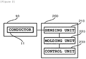
- FIG. 2 is a diagram schematically illustrating a configuration of a partial molding apparatus 200 according to an embodiment of the present invention.
- the partial molding apparatus 200 illustrated in FIG. 2 follows the embodiment, and it should be noted that constituent elements thereof are not limited to the embodiment illustrated in FIG. 2 and as necessary, some constituent elements may be added, modified, or deleted.
- the partial molding apparatus 200 may be configured to include a sensing unit 210 and a molding unit 220. Further, the partial molding apparatus 200 may further include a control unit 230 as a constituent element thereof.
- the sensing unit 210 may serve to sense the conductor 11 formed on one surface of the substrate 10.
- the sensing unit 210 may sense the voltage applied from the conductor 11.
- the present invention is not limited to a case where the sensing unit 210 senses the conductor 11.
- the sensing unit 210 may sense at least one of the electronic ink, the etching, and the insulation material, if necessary.
- the molding unit 220 may serve to cover and mold the conductor 11 sensed by the sensing unit 210 with the insulator 101.
- the molding unit 220 may effectively prevent the part which may cause the voltage interference of the protruding conductor 11 from being exposed by covering the protruding conductor 11 with the insulation cap 102 formed by the insulator 101 and fixing the insulation cap 102 by applying the insulator 101 to the insulation cap 102.
- the molding unit 220 may adjust the thickness of the insulator 101 that molds the conductor 11 based on a molding thickness of the insulator 101 set from the control unit 230.
- the molding unit 220 covers the conductor 11 with the insulator 101 twice to mold the conductor 11 with the insulator 101 having the thickness of 2 mm set by the control unit 230.
- the molding unit 220 may selectively mold only the conductor 11 positioned at a specific location of the substrate 10 based on a molding location of the insulator 101 set by the control unit 230.
- selective molding of only the conductor 11 positioned at the specific location in the molding unit 220 may be achieved by molding the conductor 11 sensed by the sensing unit 210 by the molding unit 220 when only the conductor 11 positioned at the corresponding location among one or more conductors 11 on the substrate 10 is sensed by sensing only the specific location set by the control unit 230 by the sensing unit 210, but the present invention is not limited thereto.
- the molding unit 220 may mold only the conductor 11 to which voltage equal to or higher than specific voltage sensed by the sensing unit 210 is applied.
- molding only the conductor 11 to which the voltage equal to or higher than the specific voltage is applied in the molding unit 220 may be achieved by excluding the conductor 11 to which the voltage equal to or lower than the specific voltage is applied among one or more conductors 11 sensed by the sensing unit 210 from a sensing target and molding the conductor 11 sensed by the sensing unit 210 in the molding unit 220 when the control unit 230 sets molding of the conductor 11 to which the voltage equal to or lower than the specific voltage is applied to be excluded, but the present invention is not limited thereto.
- control unit 230 may serve to control at least one of the sensing unit 210 and the molding unit 220 based on an external input.
- the external input may mean that a specific value is input by one or more of a user terminal (not illustrated) including a smart phone, a tablet, and a remote controller and input devices including a switch, and the like, but is not limited thereto.
- a user terminal not illustrated
- a smart phone including a smart phone, a tablet, and a remote controller and input devices including a switch, and the like, but is not limited thereto.
- control unit 230 may receive an input of at least one setting of setting of the molding thickness of the insulator 101 that molds the conductor 11 through the external input, setting of a sensing location on the substrate 10, and setting of molding exclusion of conductor 11 to which the voltage equal to or lower than the specific voltage is applied.
- the sensing unit 210 and the molding unit 220 are controlled based on the corresponding input, it is possible to control the molding and molding thickness of the conductor 11 on the substrate 10 according to the setting inputted through the external input.
- FIG. 3 is a diagram schematically illustrating a partial molding process using the partial molding apparatus 200 according to an embodiment of the present invention.
- the partial molding process of the partial molding method according to an embodiment of the present invention will be schematically described.
- the insulator 101 is filled in the partial molding apparatus 200 (S301).
- filling the insulator 101 may mean filling an insulating material such as silicon in a liquid state before solidification, but is not limited thereto.
- the sensing unit 210 senses one or more conductors 11 formed on the substrate 10 (S302).
- the sensing unit 210 may separately sense the conductor 11, such as a pattern formed by at least one of the electronic ink and the etching and the conductor 11 such as the protruding semiconductor device.
- step S303 when the conductor 11 is detected from the sensing unit 210, at least one conductor 11 which is sensed is covered and molded with the insulator 101 by the molding unit 220 (step S303).
- the molding unit 220 applies and solidifies the insulator 101 to the top of the conductor 11 to mold the corresponding conductor 11.
- the molding unit 220 may effectively prevent the part which may cause the voltage interference of the conductor 11 from being exposed by covering the conductor 11 with the insulation cap 102 formed by solidifying the insulator 101 and fixing the insulation cap 102 by applying the insulator 101 to the insulation cap 102.
- the molding unit 220 may adjust the molding thickness of the insulator 101 that covers the conductor 11 by adjusting the number of molding times of the conductor 11 based on the corresponding setting.
- the molding unit 220 may mold only the conductor 11 positioned at a specific location of the substrate 10 based on the corresponding setting.
- the molding unit 220 may selectively mold the conductor 11 to which the voltage equal to or higher than the specific voltage is applied among one or more conductors 11 on the substrate 10 based on the corresponding setting.
- selectively molding the conductor 11 to which the voltage equal to or higher than the specific voltage is applied may be achieved by sensing only the conductor 11 to which the voltage equal to or higher than the specific voltage is applied by the sensing unit 210 and molding the conductor 11 sensed by the sensing unit 210 by the molding unit 220 when the control unit 230 sets the molding of the conductor 11 to which the voltage equal to or lower than specific voltage is applied to be excluded, but is not limited thereto.
- filling the insulator 101 into the partial molding apparatus 200, sensing the conductor 11 by the sensing unit 210, and molding the conductor 11 by the molding unit 220 are not pre and post steps.
- At least one step of filling the insulator 101 into the partial molding apparatus 200, sensing the conductor 11 by the sensing unit 210, and molding the conductor 11 by the molding unit 220 may be added, changed, or deleted as necessary.
- the user may mold each conductor 11 by using the molding unit 220 in the process of installing the conductor 11 on the substrate 10.
- each of one or more conductors 11 to be molded may be molded by using the molding unit 220 without sensing the conductor 11 by the sensing unit 210.
Landscapes
- Engineering & Computer Science (AREA)
- Microelectronics & Electronic Packaging (AREA)
- Manufacturing & Machinery (AREA)
- Chemical & Material Sciences (AREA)
- Composite Materials (AREA)
- Mechanical Engineering (AREA)
- Physics & Mathematics (AREA)
- Electromagnetism (AREA)
- Casting Or Compression Moulding Of Plastics Or The Like (AREA)
- Moulds For Moulding Plastics Or The Like (AREA)
- Non-Metallic Protective Coatings For Printed Circuits (AREA)
Abstract
Description
- This application claims priority to and the benefit of Korean Patent Application No.
10-2017-0075870 - The present invention relates to a partially molded substrate and a partial molding apparatus and a method thereof, and more particularly, to a partially molded substrate and a partial molding apparatus and a method thereof, which cover and mold each of one or more conductors formed on a substrate with an insulator to prevent a size of the substrate from being increased due to molding, efficiently prevent high voltage from being applied between the conductors on the substrate, and prevent interference around the conductor.
- In general, when a printed circuit board (PCB) substrate is designed, in order to prevent voltage interference between conductors on a substrate, the PCB substrate needs to be designed by maintaining an isolation distance including a clearance distance and a creepage distance between the conductors.
- In the related art, since voltage applied between the conductors on the PCB substrate is low voltage, it is considered that it is not comparatively important to secure the isolation distance between the conductors, but in recent years, in the case of the PCB substrate, mounted on an electric vehicle, or the like, high voltage between the conductors on the PCB substrate is applied, and as a result, it is considered that it is important to secure the isolation distance between the conductors.
- Meanwhile, in order to prevent the voltage interference between the conductors to which the high voltage is applied, when the isolation distance between the conductors is widened, the size of the PCB substrate is increased, and as a result, a problem in that there is a limit in installing the PCB substrate in an electric device.
- For example, in the case of a recently developed and used battery pack, since an installation space of the PCB substrate for installing battery management systems (BMS) in the battery pack is limited, increasing the size of the PCB substrate due to securing the isolation distance causes substantial use of the PCB substrate to be restricted.
- Meanwhile, in recent years, a method of molding the PCB substrate with an insulator is used in order to solve such a problem and effectively prevent the voltage between the conductors on the PCB substrate from being applied.
- However, in the case of such a method, since all parts on the PCB substrate are buried in a molding due to molding, there is a problem that it is difficult to maintain and repair the parts on the PCB substrate.
- In addition, since the PCB substrate is entirely molded with the insulator, a number of parts where the insulator is used inefficiently are generated, thereby causing a problem of inefficiently increasing molding cost of the PCB substrate.
- In addition, since the PCB substrate is entirely molded, there has been a problem that the size and thickness of the PCB substrate are unnecessarily increased.
- An object of the present invention is to provide a partially molded substrate and a partial molding apparatus and a method thereof, which cover and mold each of one or more conductors formed on a substrate with an insulator to prevent the size of the substrate from being unnecessarily increased due to molding.
- Further, an object of the present invention is to provide a partially molded substrate and a partial molding apparatus and a method thereof, which cover and mold each of one or more conductors formed on a substrate with the insulator to efficiently prevent voltage between the conductors on the substrate from being applied, and prevent interference around the conductor.
- Further, an object of the present invention is to provide a partially molded substrate and a partial molding apparatus and a method thereof, which mold each of one or more conductors formed on a substrate to prevent a part on a PCB substrate including the conductor from being unnecessarily buried in the molding.
- In addition, an object of the present invention is to provide a partially molded substrate and a partial molding apparatus and a method thereof, which selectively mold any one or more conductors which need to be molded among one or more conductors formed on a substrate to efficiently use the insulator.
- Further, an object of the present invention is to provide a partially molded substrate and a partial molding apparatus and a method thereof, which efficiently use the insulator by selectively molding one or more conductors formed on a substrate to reduce design cost of the PCB substrate.
- Moreover, an object of the present invention is to provide a partially molded substrate and a partial molding apparatus and a method thereof, which selectively mold one or more conductors formed on a substrate by setting a molding thickness of an insulator to prevent a thickness of the PCB substrate from being unnecessarily increased due to the molding.
- A partially molded substrate according to an embodiment of the present invention may include one or more conductors formed on one surface, and each of one or more conductors may be covered and molded with an insulator.
- In an embodiment, in the partially molded substrate, the protruding conductor may be covered and molded with an insulation cap formed by the insulator.
- In an embodiment, in the partially molded substrate, the conductor may be covered and molded with the insulator having a predetermined thickness.
- In an embodiment, in the partially molded substrate, the conductor positioned in a predetermined molding region may be covered and molded with the insulator.
- In an embodiment, in the partially molded substrate, the conductor to which voltage equal to or higher than predetermined voltage is applied among one or more conductors is applied may be covered and molded with the insulator.
- A partial molding apparatus according to an embodiment of the present invention may include: a substrate; one or more conductors formed on one surface of the substrate; a sensing unit sensing one or more conductors; and a molding unit covering and molding each of one or more conductors sensed by the sensing unit with the insulator.
- In an embodiment, when the conductor protrudes, the molding unit may cover and mold the protruding conductor with an insulation cap formed by the insulator.
- In an embodiment, when a molding thickness is set, the molding unit may cover and mold the conductor with the insulator in the set thickness.
- In an embodiment, when a molding region is set, the molding unit may cover and mold the conductor positioned in the set molding region with the insulator.
- In an embodiment, the sensing unit may sense voltage applied from the conductor.
- In an embodiment, the molding unit may cover and mold the conductor to which voltage equal to or higher than predetermined voltage is applied among one or more conductors sensed by the sensing unit with the insulator.
- A partial molding method according to an embodiment of the present invention may include: filling an insulator; sensing one or more conductors formed on one surface of a substrate; and covering and molding each of one or more sensed with the insulator.
- In an embodiment, in the molding, when the conductor protrudes, the protruding conductor may be covered and molded with an insulation cap formed by the insulator.
- In an embodiment, in the molding, when a molding thickness is set, the conductor may be covered and molded with the insulator in the set thickness.
- In an embodiment, in the molding, when a molding region is set, the conductor positioned in the set molding region may be covered and molded with the insulator.
- In an embodiment, in the sensing, the voltage applied from the conductor may be sensed.
- In an embodiment, in the molding, the conductor to which voltage equal to or higher than predetermined voltage is applied among one or more sensed conductors may be covered and molded with the insulator.
- According to an aspect of the present invention, provided are a partially molded substrate and a partial molding apparatus and a method thereof, which cover and mold each of one or more conductors formed on a substrate with an insulator to prevent the size of the substrate from being unnecessarily increased due to molding.
- Further, according to another aspect of the present invention, provided are a partially molded substrate and a partial molding apparatus and a method thereof, which cover and mold each of one or more conductors formed on the substrate with the insulator to efficiently prevent voltage between the conductors on the substrate from being applied, and prevent interference around the conductor.
- In addition, according to yet another aspect of the present invention, provided are a partially molded substrate and a partial molding apparatus and a method thereof, which mold each of one or more conductors formed on the substrate to prevent a part on a PCB substrate including the conductor from being unnecessarily buried in the molding.
- Further, according to still yet another aspect of the present invention, provided are a partially molded substrate and a partial molding apparatus and a method thereof, which selectively mold one or more conductors which need to be molded among one or more conductors formed on the substrate to efficiently use the insulator.
- Moreover, according to still yet another aspect of the present invention, provided are a partially molded substrate and a partial molding apparatus and a method thereof, which efficiently use the insulator by selectively molding one or more conductors formed on the substrate to reduce design cost of the PCB substrate.
- In addition, according to still yet another aspect of the present invention, provided are a partially molded substrate and a partial molding apparatus and a method thereof, which selectively mold one or more conductors formed on the substrate by setting a molding thickness of the insulator to prevent a thickness of the PCB substrate from being unnecessarily increased due to the molding.
-
-
FIG. 1 is a diagram schematically illustrating a partially molded substrate according to an embodiment of the present invention. -
FIG. 2 is a diagram schematically illustrating a configuration of a partial molding apparatus according to an embodiment of the present invention. -
FIG. 3 is a diagram schematically illustrating a partial molding process of the partial molding apparatus according to an embodiment of the present invention. - The present invention will be described below in detail with reference to the accompanying drawings. Herein, the repeated description and the detailed description of publicly-known function and configuration that may make the gist of the present invention unnecessarily ambiguous will be omitted. Embodiments of the present invention are provided for more completely describing the present invention to those skilled in the art. Accordingly, shapes, sizes, and the like of elements in the drawings may be exaggerated for clearer explanation.
- Throughout the specification, unless explicitly described to the contrary, a case where any part "includes" any component will be understood to imply the inclusion of stated components but not the exclusion of any other component.
- In addition, the term "unit" disclosed in the specification means a unit that processes at least one function or operation, and the unit may be implemented by hardware or software or a combination of hardware and software.
-
FIG. 1 is a diagram schematically illustrating a partially moldedsubstrate 100 according to an embodiment of the present invention. - However, the partially molded
substrate 100 illustrated inFIG. 1 follows the embodiment and it should be noted that constituent elements and a shape thereof are not limited to those illustrated inFIG. 1 and as necessary, some constituent elements and shapes may be added, modified, or deleted. - First, referring to
FIG. 1 , the partially moldedsubstrate 100 according to an embodiment of the present invention may be implemented in a type in which a conductor 11 (for example, a pattern implemented by a semiconductor device and electronic ink, and the like) having conductivity of asubstrate 10 in the related art is covered and molded with each of at least one of aninsulator 101 and aninsulation cap 102 having an insulating property. - In this case, the
conductor 11 as an object having the conductivity, which is formed on one surface of thesubstrate 10 may include a pattern implemented by at least one of electronic ink and etching, and the like. - Further, it is noted that that the partially molded
substrate 100 may be implemented as a printed circuit board (PCB) including a semiconductor device, but is not limited thereto. - Meanwhile, the
insulator 101 according to an embodiment of the present invention covers and molds theconductor 11 and molds each of one ormore conductors 11 to prevent voltage from being applied from any oneconductor 11 among one ormore conductors 11 to anotherconductor 11. - Herein, the thickness of the
insulator 101 covering theconductor 11 may be controlled by apartial molding apparatus 200 described below. - In addition, the
insulator 101 may be implemented as an insulating material including silicon, insulating rubber, and the like, but is not limited thereto. - In addition, when a liquid-state insulation material is filled and applied in the
partial molding apparatus 200 to be described below, theinsulator 101 may be formed by solidifying the applied liquid-state insulation material, but the present invention is not limited thereto. - For example, the
insulator 101 is applied to the top of theconductor 11 by amolding unit 220 to be described below and solidified to cover and mold theconductor 11. - Meanwhile, a part which may cause voltage interference of the protruding
conductor 11 among one ormore conductors 11 of thesubstrate 10 may be covered and molded with a cap-shapedinsulation cap 102 formed by theinsulator 101. - For example, when the protruding
conductor 11 is covered with theinsulation cap 102 and theinsulator 101 is applied to the correspondinginsulation cap 102, the correspondinginsulation cap 102 is fixed by the solidifiedinsulator 101 to effectively prevent the voltage from being applied from the protrudingconductor 11 to anotherconductor 11. -
FIG. 2 is a diagram schematically illustrating a configuration of apartial molding apparatus 200 according to an embodiment of the present invention. - However, the
partial molding apparatus 200 illustrated inFIG. 2 follows the embodiment, and it should be noted that constituent elements thereof are not limited to the embodiment illustrated inFIG. 2 and as necessary, some constituent elements may be added, modified, or deleted. - Referring to
FIG. 2 , thepartial molding apparatus 200 according to an embodiment of the present invention may be configured to include asensing unit 210 and amolding unit 220. Further, thepartial molding apparatus 200 may further include acontrol unit 230 as a constituent element thereof. - First, the
sensing unit 210 may serve to sense theconductor 11 formed on one surface of thesubstrate 10. - Moreover, the
sensing unit 210 may sense the voltage applied from theconductor 11. - However, herein, it is noted that the present invention is not limited to a case where the
sensing unit 210 senses theconductor 11. - For example, the
sensing unit 210 may sense at least one of the electronic ink, the etching, and the insulation material, if necessary. - Next, the
molding unit 220 may serve to cover and mold theconductor 11 sensed by thesensing unit 210 with theinsulator 101. - Meanwhile, when the
conductor 11 of thesubstrate 10 protrudes, themolding unit 220 may effectively prevent the part which may cause the voltage interference of the protrudingconductor 11 from being exposed by covering the protrudingconductor 11 with theinsulation cap 102 formed by theinsulator 101 and fixing theinsulation cap 102 by applying theinsulator 101 to theinsulation cap 102. - Further, the
molding unit 220 may adjust the thickness of theinsulator 101 that molds theconductor 11 based on a molding thickness of theinsulator 101 set from thecontrol unit 230. - For example, when a basic thickness of the
insulator 101 is 1 mm and the molding thickness of theinsulator 101 set by thecontrol unit 230 is 2 mm, themolding unit 220 covers theconductor 11 with theinsulator 101 twice to mold theconductor 11 with theinsulator 101 having the thickness of 2 mm set by thecontrol unit 230. - Further, the
molding unit 220 may selectively mold only theconductor 11 positioned at a specific location of thesubstrate 10 based on a molding location of theinsulator 101 set by thecontrol unit 230. - In this case, selective molding of only the
conductor 11 positioned at the specific location in themolding unit 220 may be achieved by molding theconductor 11 sensed by thesensing unit 210 by themolding unit 220 when only theconductor 11 positioned at the corresponding location among one ormore conductors 11 on thesubstrate 10 is sensed by sensing only the specific location set by thecontrol unit 230 by thesensing unit 210, but the present invention is not limited thereto. - Moreover, when a user excludes the molding of the
conductor 11 to which voltage equal to or lower than specific voltage is applied through thecontrol unit 230, themolding unit 220 may mold only theconductor 11 to which voltage equal to or higher than specific voltage sensed by thesensing unit 210 is applied. - For example, molding only the
conductor 11 to which the voltage equal to or higher than the specific voltage is applied in themolding unit 220 may be achieved by excluding theconductor 11 to which the voltage equal to or lower than the specific voltage is applied among one ormore conductors 11 sensed by thesensing unit 210 from a sensing target and molding theconductor 11 sensed by thesensing unit 210 in themolding unit 220 when thecontrol unit 230 sets molding of theconductor 11 to which the voltage equal to or lower than the specific voltage is applied to be excluded, but the present invention is not limited thereto. - Next, the
control unit 230 may serve to control at least one of thesensing unit 210 and themolding unit 220 based on an external input. - Herein, the external input may mean that a specific value is input by one or more of a user terminal (not illustrated) including a smart phone, a tablet, and a remote controller and input devices including a switch, and the like, but is not limited thereto.
- Meanwhile, the
control unit 230 may receive an input of at least one setting of setting of the molding thickness of theinsulator 101 that molds theconductor 11 through the external input, setting of a sensing location on thesubstrate 10, and setting of molding exclusion ofconductor 11 to which the voltage equal to or lower than the specific voltage is applied. - Further, by controlling at least one of the
sensing unit 210 and themolding unit 220 based on the corresponding input, it is possible to control the molding and molding thickness of theconductor 11 on thesubstrate 10 according to the setting inputted through the external input. -
FIG. 3 is a diagram schematically illustrating a partial molding process using thepartial molding apparatus 200 according to an embodiment of the present invention. - However, the partial molding method illustrated in
FIG. 3 follows the embodiment and it should be noted that the process thereof is not limited to the embodiment illustrated inFIG. 3 and as necessary, some processes may be added, modified, or deleted. - Referring to
FIG. 3 , the partial molding process of the partial molding method according to an embodiment of the present invention will be schematically described. First, theinsulator 101 is filled in the partial molding apparatus 200 (S301). - In this case, filling the
insulator 101 may mean filling an insulating material such as silicon in a liquid state before solidification, but is not limited thereto. - Next, the
sensing unit 210 senses one ormore conductors 11 formed on the substrate 10 (S302). - Herein, the
sensing unit 210 may separately sense theconductor 11, such as a pattern formed by at least one of the electronic ink and the etching and theconductor 11 such as the protruding semiconductor device. - Meanwhile, when the
conductor 11 is detected from thesensing unit 210, at least oneconductor 11 which is sensed is covered and molded with theinsulator 101 by the molding unit 220 (step S303). - In this case, when the
conductor 11 sensed by thesensing unit 210 is theconductor 11 such as the pattern formed by at least one of the electronic ink and the etching, themolding unit 220 applies and solidifies theinsulator 101 to the top of theconductor 11 to mold the correspondingconductor 11. - Further, when the
conductor 11 sensed by thesensing unit 210 is theconductor 11 such as the protruding semiconductor device, themolding unit 220 may effectively prevent the part which may cause the voltage interference of theconductor 11 from being exposed by covering theconductor 11 with theinsulation cap 102 formed by solidifying theinsulator 101 and fixing theinsulation cap 102 by applying theinsulator 101 to theinsulation cap 102. - Moreover, when the molding thickness of the
insulator 101 is set by thecontrol unit 230, themolding unit 220 may adjust the molding thickness of theinsulator 101 that covers theconductor 11 by adjusting the number of molding times of theconductor 11 based on the corresponding setting. - Besides, when the molding location of the
insulator 101 is set by thecontrol unit 230, themolding unit 220 may mold only theconductor 11 positioned at a specific location of thesubstrate 10 based on the corresponding setting. - Further, when the
control unit 230 sets the molding of theconductor 11 to which the voltage equal to or lower than the specific voltage is applied to be excluded, themolding unit 220 may selectively mold theconductor 11 to which the voltage equal to or higher than the specific voltage is applied among one ormore conductors 11 on thesubstrate 10 based on the corresponding setting. - In this case, selectively molding the
conductor 11 to which the voltage equal to or higher than the specific voltage is applied may be achieved by sensing only theconductor 11 to which the voltage equal to or higher than the specific voltage is applied by thesensing unit 210 and molding theconductor 11 sensed by thesensing unit 210 by themolding unit 220 when thecontrol unit 230 sets the molding of theconductor 11 to which the voltage equal to or lower than specific voltage is applied to be excluded, but is not limited thereto. - Meanwhile, it is noted that filling the
insulator 101 into thepartial molding apparatus 200, sensing theconductor 11 by thesensing unit 210, and molding theconductor 11 by themolding unit 220 are not pre and post steps. - In addition, it is noted that at least one step of filling the
insulator 101 into thepartial molding apparatus 200, sensing theconductor 11 by thesensing unit 210, and molding theconductor 11 by themolding unit 220 may be added, changed, or deleted as necessary. - For example, when the user personally designs the
substrate 10 including theconductor 11, the user may mold eachconductor 11 by using themolding unit 220 in the process of installing theconductor 11 on thesubstrate 10. - Further, when the user personally designs the
substrate 10 including theconductor 11, the user recognizes the location of theconductor 11 on thesubstrate 10, and as a result, each of one ormore conductors 11 to be molded may be molded by using themolding unit 220 without sensing theconductor 11 by thesensing unit 210. - Hereinabove, a specific embodiment of the present invention has been illustrated and described, but the technical spirit of the present invention is not limited to the accompanying drawings and the described contents and it is apparent to those skilled in the art that various modifications of the present invention can be made within the scope without departing from the spirit of the present invention and it will be understood that the modifications are included in the claims of the present invention without departing from the spirit of the present invention.
Claims (15)
- A partially molded substrate comprising:one or more conductors formed on one surface,wherein each of one or more conductors is covered and molded with an insulator.
- The partially molded substrate of claim 1, wherein in the partially molded substrate, the protruding conductor is covered and molded with an insulation cap formed by the insulator.
- The partially molded substrate of claim 1, wherein in the partially molded substrate, the conductor is covered and molded with the insulator having a predetermined thickness.
- The partially molded substrate of claim 1, wherein in the partially molded substrate, the conductor positioned in a predetermined molding region is covered and molded with the insulator.
- The partially molded substrate of claim 1, wherein in the partially molded substrate, the conductor to which voltage equal to or higher than predetermined voltage among one or more conductors is applied is covered and molded with the insulator.
- A partial molding apparatus comprising:a substrate;one or more conductors formed on one surface of the substrate;a sensing unit sensing one or more conductors; anda molding unit covering and molding each of one or more conductors sensed by the sensing unit with the insulator.
- The partial molding apparatus of claim 6, wherein when the conductor protrudes, the molding unit covers and molds the protruding conductor with an insulation cap formed by the insulator.
- The partial molding apparatus of claim 6, wherein when a molding thickness is set, the molding unit covers and molds the conductor with the insulator in the set thickness.
- The partial molding apparatus of claim 6, wherein when a molding region is set, the molding unit covers and molds the conductor positioned in the set molding region with the insulator.
- The partial molding apparatus of claim 6, wherein the sensing unit senses voltage applied from the conductor, and
the molding unit covers and molds the conductor to which voltage equal to or higher than predetermined voltage is applied among one or more conductors sensed by the sensing unit with the insulator. - A partial molding method comprising:filling an insulator;sensing one or more conductors formed on one surface of a substrate; andcovering and molding each of one or more sensed conductors with the insulator.
- The partial molding method of claim 11, wherein in the molding, when the conductor protrudes, the protruding conductor is covered and molded with an insulation cap formed by the insulator.
- The partial molding method of claim 11, wherein in the molding, when a molding thickness is set, the conductor is covered and molded with the insulator in the set thickness.
- The partial molding method of claim 11, wherein in the molding, when a molding region is set, the conductor positioned in the set molding region is covered and molded with the insulator.
- The partial molding method of claim 11, wherein in the sensing, the voltage applied from the conductor is sensed, and
in the molding, the conductor to which voltage equal to or higher than predetermined voltage is applied among one or more sensed conductors is covered and molded with the insulator.
Applications Claiming Priority (2)
| Application Number | Priority Date | Filing Date | Title |
|---|---|---|---|
| KR1020170075870A KR102186090B1 (en) | 2017-06-15 | 2017-06-15 | Apparatus and method for partially molding of printed circuit board, and printed circuit board produced therefrom |
| PCT/KR2018/002129 WO2018230811A1 (en) | 2017-06-15 | 2018-02-21 | Partially molded substrate and partial molding device and method |
Publications (2)
| Publication Number | Publication Date |
|---|---|
| EP3579668A1 true EP3579668A1 (en) | 2019-12-11 |
| EP3579668A4 EP3579668A4 (en) | 2020-03-25 |
Family
ID=64659137
Family Applications (1)
| Application Number | Title | Priority Date | Filing Date |
|---|---|---|---|
| EP18818161.4A Pending EP3579668A4 (en) | 2017-06-15 | 2018-02-21 | PARTIALLY MOLDED SUBSTRATE AND PARTIAL MOLDING DEVICE AND METHOD |
Country Status (6)
| Country | Link |
|---|---|
| US (1) | US10939542B2 (en) |
| EP (1) | EP3579668A4 (en) |
| JP (1) | JP6849249B2 (en) |
| KR (1) | KR102186090B1 (en) |
| CN (1) | CN110313222B (en) |
| WO (1) | WO2018230811A1 (en) |
Family Cites Families (31)
| Publication number | Priority date | Publication date | Assignee | Title |
|---|---|---|---|---|
| US3964845A (en) * | 1974-12-26 | 1976-06-22 | Schlumberger Technology Corporation | Apparatus for repairing conductor insulation |
| US5160374A (en) * | 1990-07-24 | 1992-11-03 | The United States Of America As Represented By The Secretary Of The Air Force | Process and apparatus for preventing the pulse discharge of insulators in ionizing radiation |
| US5450286A (en) * | 1992-12-04 | 1995-09-12 | Parlex Corporation | Printed circuit having a dielectric covercoat |
| TW311267B (en) * | 1994-04-11 | 1997-07-21 | Raychem Ltd | |
| JP3651496B2 (en) * | 1995-06-02 | 2005-05-25 | 住友電気工業株式会社 | Molding device for power cable end connection |
| JPH10209338A (en) * | 1997-01-22 | 1998-08-07 | Matsushita Electric Ind Co Ltd | Semiconductor circuit device and method of manufacturing the same |
| JP2000188298A (en) * | 1998-12-21 | 2000-07-04 | Yazaki Corp | Method for sealing electronic components |
| JP2001007451A (en) * | 1999-06-21 | 2001-01-12 | Matsushita Electric Ind Co Ltd | Circuit board and method of manufacturing the same |
| JP4249360B2 (en) * | 1999-11-02 | 2009-04-02 | 日東電工株式会社 | Circuit board and manufacturing method thereof |
| WO2006101274A1 (en) * | 2005-03-25 | 2006-09-28 | Fujifilm Corporation | Method of manufacturing solid state imaging device |
| US7928010B2 (en) * | 2006-10-20 | 2011-04-19 | Sandisk Corporation | Method for producing portable memory devices |
| JP2008159744A (en) * | 2006-12-22 | 2008-07-10 | Konica Minolta Medical & Graphic Inc | Electronic component sealing material, method for forming the same, and sealing material forming apparatus |
| US7633055B2 (en) * | 2007-03-08 | 2009-12-15 | Lumination Llc | Sealed light emitting diode assemblies including annular gaskets and methods of making same |
| KR100860528B1 (en) * | 2007-05-04 | 2008-09-26 | 엘에스산전 주식회사 | High voltage load switchgear and its manufacturing method |
| US20110260945A1 (en) * | 2007-08-03 | 2011-10-27 | Fumio Karasawa | Coating Composition and Article Using the Same |
| JP2009043823A (en) * | 2007-08-07 | 2009-02-26 | Hitachi-Lg Data Storage Inc | Method for sticking non-insulating sheet to printed wiring board, printed wiring board, and optical disk device |
| JP2009051876A (en) | 2007-08-23 | 2009-03-12 | Three M Innovative Properties Co | Coating composition and article using the same |
| JP5395625B2 (en) * | 2009-11-11 | 2014-01-22 | 日東電工株式会社 | Wiring circuit board and fuel cell |
| JP5511621B2 (en) | 2010-10-13 | 2014-06-04 | 三菱電機株式会社 | Semiconductor device |
| JP5209038B2 (en) * | 2010-12-08 | 2013-06-12 | 日立オートモティブシステムズ株式会社 | Connector and manufacturing method thereof |
| JP2013008810A (en) * | 2011-06-24 | 2013-01-10 | Sumitomo Electric Ind Ltd | Method of manufacturing printed wiring board, and printed wiring board |
| KR20130046487A (en) | 2011-10-28 | 2013-05-08 | 삼성전기주식회사 | Semiconductor package |
| DE102011088028B3 (en) * | 2011-12-08 | 2013-03-28 | Siemens Aktiengesellschaft | Power amplifier device for magnetic resonance device used in clinical applications of imaging, has two transistors that are arranged in parallel planes and are connected at opposed sides of cooling passage for refrigeration |
| KR101388815B1 (en) | 2012-06-29 | 2014-04-23 | 삼성전기주식회사 | Semiconductor package |
| KR102177502B1 (en) * | 2013-11-20 | 2020-11-11 | 삼성에스디아이 주식회사 | Integrated silicone for protecting electronic devices, circuit module using the same, and the method thereof |
| KR20150073620A (en) | 2013-12-23 | 2015-07-01 | 엘에스파워세미텍 주식회사 | Semiconductor package decreasable size |
| JP2015156423A (en) * | 2014-02-20 | 2015-08-27 | ローム株式会社 | semiconductor device |
| KR102204749B1 (en) | 2014-04-01 | 2021-01-20 | 주식회사 솔루엠 | Coil component and manufacturing method there of |
| US20150279547A1 (en) | 2014-04-01 | 2015-10-01 | Samsung Electro-Mechanics Co., Ltd. | Coil component and manufacturing method thereof |
| KR101806145B1 (en) | 2015-12-23 | 2017-12-08 | 주식회사 포스코 | Frame structure |
| KR102528424B1 (en) * | 2016-08-31 | 2023-05-04 | 삼성전자주식회사 | Electric component and electronic device with the same |
-
2017
- 2017-06-15 KR KR1020170075870A patent/KR102186090B1/en active Active
-
2018
- 2018-02-21 WO PCT/KR2018/002129 patent/WO2018230811A1/en not_active Ceased
- 2018-02-21 JP JP2019544020A patent/JP6849249B2/en active Active
- 2018-02-21 EP EP18818161.4A patent/EP3579668A4/en active Pending
- 2018-02-21 CN CN201880012102.1A patent/CN110313222B/en active Active
-
2019
- 2019-09-25 US US16/581,866 patent/US10939542B2/en active Active
Also Published As
| Publication number | Publication date |
|---|---|
| JP2020508567A (en) | 2020-03-19 |
| JP6849249B2 (en) | 2021-03-24 |
| KR20180136739A (en) | 2018-12-26 |
| US10939542B2 (en) | 2021-03-02 |
| EP3579668A4 (en) | 2020-03-25 |
| WO2018230811A1 (en) | 2018-12-20 |
| CN110313222B (en) | 2022-04-01 |
| KR102186090B1 (en) | 2020-12-03 |
| US20200022254A1 (en) | 2020-01-16 |
| CN110313222A (en) | 2019-10-08 |
Similar Documents
| Publication | Publication Date | Title |
|---|---|---|
| US10477713B2 (en) | Single-piece metal housing with integral antennas | |
| US20230411385A1 (en) | Package with embedded capacitors | |
| JP6798436B2 (en) | Circuit equipment, circuit equipment manufacturing methods, and connectors | |
| US11705377B2 (en) | Stacked die cavity package | |
| US9526188B2 (en) | Electronic device package box | |
| WO2013104274A1 (en) | Method for manufacturing circuit board, circuit board and electronic apparatus | |
| US10998275B2 (en) | Package with cathodic protection for corrosion mitigation | |
| CN107438467B (en) | Device for connecting a planar body to a voltage supply | |
| US10939542B2 (en) | Partially molded substrate and partial molding device and method | |
| US11158568B2 (en) | Package with wall-side capacitors | |
| US20190333832A1 (en) | Bi-layer prepreg for reduced dielectric thickness | |
| JP2013069832A (en) | Control device of apparatus | |
| EP3506348B1 (en) | Thin film passive devices integrated in a package substrate | |
| US20160197433A1 (en) | Waterproof receptacle connector | |
| JP2010041625A (en) | Onboard waterproof antenna apparatus and waterproof molding method thereof | |
| WO2022203383A1 (en) | Housing comprising plating layer and electronic device comprising housing | |
| JP6083357B2 (en) | Electronic equipment | |
| US10317952B2 (en) | Compartment for magnet placement | |
| US20190169020A1 (en) | Package substrate integrated devices | |
| KR20160100593A (en) | Apparatus for generating electromagnetic field | |
| WO2018125124A1 (en) | Creating dielectric helmet films using pulsed gas deposition | |
| JP2006066487A (en) | Manufacturing method of electronic component device | |
| HK1033036A (en) | Contact-connector module for mobile telephone apparatuses | |
| CN105226042A (en) | Packaging substrate and manufacturing method thereof |
Legal Events
| Date | Code | Title | Description |
|---|---|---|---|
| STAA | Information on the status of an ep patent application or granted ep patent |
Free format text: STATUS: THE INTERNATIONAL PUBLICATION HAS BEEN MADE |
|
| PUAI | Public reference made under article 153(3) epc to a published international application that has entered the european phase |
Free format text: ORIGINAL CODE: 0009012 |
|
| STAA | Information on the status of an ep patent application or granted ep patent |
Free format text: STATUS: REQUEST FOR EXAMINATION WAS MADE |
|
| 17P | Request for examination filed |
Effective date: 20190902 |
|
| AK | Designated contracting states |
Kind code of ref document: A1 Designated state(s): AL AT BE BG CH CY CZ DE DK EE ES FI FR GB GR HR HU IE IS IT LI LT LU LV MC MK MT NL NO PL PT RO RS SE SI SK SM TR |
|
| AX | Request for extension of the european patent |
Extension state: BA ME |
|
| A4 | Supplementary search report drawn up and despatched |
Effective date: 20200221 |
|
| RIC1 | Information provided on ipc code assigned before grant |
Ipc: H05K 1/02 20060101ALI20200217BHEP Ipc: H05K 3/28 20060101ALI20200217BHEP Ipc: H05K 3/00 20060101ALI20200217BHEP Ipc: H05K 1/05 20060101AFI20200217BHEP |
|
| DAV | Request for validation of the european patent (deleted) | ||
| DAX | Request for extension of the european patent (deleted) | ||
| RAP1 | Party data changed (applicant data changed or rights of an application transferred) |
Owner name: LG ENERGY SOLUTION LTD. |
|
| RAP3 | Party data changed (applicant data changed or rights of an application transferred) |
Owner name: LG ENERGY SOLUTION, LTD. |
|
| STAA | Information on the status of an ep patent application or granted ep patent |
Free format text: STATUS: EXAMINATION IS IN PROGRESS |
|
| 17Q | First examination report despatched |
Effective date: 20220804 |