EP3579151B1 - Herstellungsverfahren eines rechners mit rekurrenten neuronalen netzen - Google Patents
Herstellungsverfahren eines rechners mit rekurrenten neuronalen netzen Download PDFInfo
- Publication number
- EP3579151B1 EP3579151B1 EP19177078.3A EP19177078A EP3579151B1 EP 3579151 B1 EP3579151 B1 EP 3579151B1 EP 19177078 A EP19177078 A EP 19177078A EP 3579151 B1 EP3579151 B1 EP 3579151B1
- Authority
- EP
- European Patent Office
- Prior art keywords
- layer
- electrode
- block copolymers
- forming
- denoted
- Prior art date
- Legal status (The legal status is an assumption and is not a legal conclusion. Google has not performed a legal analysis and makes no representation as to the accuracy of the status listed.)
- Active
Links
Images


Classifications
-
- G—PHYSICS
- G06—COMPUTING OR CALCULATING; COUNTING
- G06N—COMPUTING ARRANGEMENTS BASED ON SPECIFIC COMPUTATIONAL MODELS
- G06N3/00—Computing arrangements based on biological models
- G06N3/02—Neural networks
- G06N3/06—Physical realisation, i.e. hardware implementation of neural networks, neurons or parts of neurons
- G06N3/063—Physical realisation, i.e. hardware implementation of neural networks, neurons or parts of neurons using electronic means
- G06N3/065—Analogue means
-
- G—PHYSICS
- G06—COMPUTING OR CALCULATING; COUNTING
- G06N—COMPUTING ARRANGEMENTS BASED ON SPECIFIC COMPUTATIONAL MODELS
- G06N3/00—Computing arrangements based on biological models
- G06N3/02—Neural networks
- G06N3/04—Architecture, e.g. interconnection topology
- G06N3/044—Recurrent networks, e.g. Hopfield networks
- G06N3/0442—Recurrent networks, e.g. Hopfield networks characterised by memory or gating, e.g. long short-term memory [LSTM] or gated recurrent units [GRU]
-
- G—PHYSICS
- G06—COMPUTING OR CALCULATING; COUNTING
- G06N—COMPUTING ARRANGEMENTS BASED ON SPECIFIC COMPUTATIONAL MODELS
- G06N3/00—Computing arrangements based on biological models
- G06N3/02—Neural networks
- G06N3/04—Architecture, e.g. interconnection topology
- G06N3/0495—Quantised networks; Sparse networks; Compressed networks
-
- G—PHYSICS
- G06—COMPUTING OR CALCULATING; COUNTING
- G06N—COMPUTING ARRANGEMENTS BASED ON SPECIFIC COMPUTATIONAL MODELS
- G06N3/00—Computing arrangements based on biological models
- G06N3/02—Neural networks
- G06N3/08—Learning methods
- G06N3/09—Supervised learning
-
- H—ELECTRICITY
- H10—SEMICONDUCTOR DEVICES; ELECTRIC SOLID-STATE DEVICES NOT OTHERWISE PROVIDED FOR
- H10B—ELECTRONIC MEMORY DEVICES
- H10B63/00—Resistance change memory devices, e.g. resistive RAM [ReRAM] devices
- H10B63/80—Arrangements comprising multiple bistable or multi-stable switching components of the same type on a plane parallel to the substrate, e.g. cross-point arrays
- H10B63/82—Arrangements comprising multiple bistable or multi-stable switching components of the same type on a plane parallel to the substrate, e.g. cross-point arrays the switching components having a common active material layer
-
- H—ELECTRICITY
- H10—SEMICONDUCTOR DEVICES; ELECTRIC SOLID-STATE DEVICES NOT OTHERWISE PROVIDED FOR
- H10N—ELECTRIC SOLID-STATE DEVICES NOT OTHERWISE PROVIDED FOR
- H10N70/00—Solid-state devices having no potential barriers, and specially adapted for rectifying, amplifying, oscillating or switching
- H10N70/011—Manufacture or treatment of multistable switching devices
-
- H—ELECTRICITY
- H10—SEMICONDUCTOR DEVICES; ELECTRIC SOLID-STATE DEVICES NOT OTHERWISE PROVIDED FOR
- H10N—ELECTRIC SOLID-STATE DEVICES NOT OTHERWISE PROVIDED FOR
- H10N70/00—Solid-state devices having no potential barriers, and specially adapted for rectifying, amplifying, oscillating or switching
- H10N70/20—Multistable switching devices, e.g. memristors
-
- H—ELECTRICITY
- H10—SEMICONDUCTOR DEVICES; ELECTRIC SOLID-STATE DEVICES NOT OTHERWISE PROVIDED FOR
- H10N—ELECTRIC SOLID-STATE DEVICES NOT OTHERWISE PROVIDED FOR
- H10N70/00—Solid-state devices having no potential barriers, and specially adapted for rectifying, amplifying, oscillating or switching
- H10N70/801—Constructional details of multistable switching devices
- H10N70/821—Device geometry
- H10N70/826—Device geometry adapted for essentially vertical current flow, e.g. sandwich or pillar type devices
-
- H—ELECTRICITY
- H10—SEMICONDUCTOR DEVICES; ELECTRIC SOLID-STATE DEVICES NOT OTHERWISE PROVIDED FOR
- H10N—ELECTRIC SOLID-STATE DEVICES NOT OTHERWISE PROVIDED FOR
- H10N70/00—Solid-state devices having no potential barriers, and specially adapted for rectifying, amplifying, oscillating or switching
- H10N70/801—Constructional details of multistable switching devices
- H10N70/841—Electrodes
-
- H—ELECTRICITY
- H10—SEMICONDUCTOR DEVICES; ELECTRIC SOLID-STATE DEVICES NOT OTHERWISE PROVIDED FOR
- H10N—ELECTRIC SOLID-STATE DEVICES NOT OTHERWISE PROVIDED FOR
- H10N70/00—Solid-state devices having no potential barriers, and specially adapted for rectifying, amplifying, oscillating or switching
- H10N70/801—Constructional details of multistable switching devices
- H10N70/881—Switching materials
- H10N70/882—Compounds of sulfur, selenium or tellurium, e.g. chalcogenides
- H10N70/8825—Selenides, e.g. GeSe
-
- H—ELECTRICITY
- H10—SEMICONDUCTOR DEVICES; ELECTRIC SOLID-STATE DEVICES NOT OTHERWISE PROVIDED FOR
- H10N—ELECTRIC SOLID-STATE DEVICES NOT OTHERWISE PROVIDED FOR
- H10N70/00—Solid-state devices having no potential barriers, and specially adapted for rectifying, amplifying, oscillating or switching
- H10N70/801—Constructional details of multistable switching devices
- H10N70/881—Switching materials
- H10N70/882—Compounds of sulfur, selenium or tellurium, e.g. chalcogenides
- H10N70/8828—Tellurides, e.g. GeSbTe
-
- H—ELECTRICITY
- H10—SEMICONDUCTOR DEVICES; ELECTRIC SOLID-STATE DEVICES NOT OTHERWISE PROVIDED FOR
- H10N—ELECTRIC SOLID-STATE DEVICES NOT OTHERWISE PROVIDED FOR
- H10N70/00—Solid-state devices having no potential barriers, and specially adapted for rectifying, amplifying, oscillating or switching
- H10N70/801—Constructional details of multistable switching devices
- H10N70/881—Switching materials
- H10N70/883—Oxides or nitrides
- H10N70/8833—Binary metal oxides, e.g. TaOx
Definitions
- the principle of this paradigm is to project the input layer towards the reservoir, then to modify the connections going from the reservoir to the output layer by a supervised learning.
- the invention relates to a computer which is a physical or material (“ hardware ”) implementation of the “ Reservoir computing ” paradigm.
- the invention finds its application in particular in the classification of tasks, the extraction of characteristics, the pursuit of objects (" tracking" in English), the prediction of movements in robotics, voice recognition and sound recognition.
- a method of manufacturing a recurrent neural network computer comprises a step of random growth of silver nanowires on a structured platinum electrode. The randomness is obtained by a preliminary step of forming copper microspheres on the structured electrode. The copper microspheres form a seed layer for the silver nanowires.
- the method comprises a step of sulfurization of the silver nanowires so as to obtain structures of the Ag / Ag 2 S / Ag type. Such structures form resistive memory cells of the atomic switch type.
- Such a method of the state of the art allows the manufacture of a computer which is a physical implementation of the “Reservoir computing ” paradigm.
- a method of the state of the art is not entirely satisfactory insofar as the choice of materials for the resistive memory is restricted.
- block copolymers have the property of self-assembling into dense networks of nanometric objects with the capacity to form a lithography mask.
- the lithography mask thus formed by the first and second layers of block copolymers makes it possible to structure the dielectric layer and the second electrode during steps c) and h).
- the first electrode is also structured during step d ′) by being formed on the structured dielectric layer, for example by conformal deposition.
- the memory layer is also structured during step e) by being formed on the first structured electrode, for example by conformal deposition.
- the method according to the invention may include one or more of the following characteristics.
- random polymer is meant a polymer having a random ball.
- the layer of the random polymer is a functionalization layer making it possible to control the surface energies of the dielectric layer.
- the layer of the random polymer is a functionalization layer making it possible to control the surface energies of the second electrode.
- An advantage provided is to accentuate the randomness and improve the quality of the formation of the second layer of block copolymers.
- the randomness is accentuated by the surface topology of the memory layer resulting from the structuring of the dielectric layer during step c).
- the random polymer is selected from the group comprising a random copolymer, a homopolymer, a self-assembled monolayer.
- the memory layer is made of at least one material selected from the group comprising HfO 2 , Al 2 O 3 , SiO 2 , ZrO, a titanium oxide, a chalcogenide, Ta 2 O 5 .
- the first and second electrodes are made of at least one material selected from the group comprising Ti, TiN, Pt, Zr, Al, Hf, Ta, TaN, C, Cu, Ag.
- the first layer of block copolymers and the second layer of block copolymers formed respectively during steps b) and g) have a thickness of between 30 nm and 50 nm.
- an advantage obtained is to obtain a lithography mask of good quality for structuring the dielectric layer and the second electrode.
- the method comprises a step j) consisting in forming an encapsulation layer on the second structured electrode during step h), step j) being executed after step i).
- an advantage obtained is to protect the computer from air and humidity.
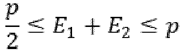
- the dielectric layer structured during step c) has a pitch, denoted p, and in which steps d ′) and e) are carried out so that the first electrode and the memory layer have respectively of the first and second thicknesses, denoted E 1 and E 2 , verifying: p 2 ⁇ E 1 + E 2 ⁇ p
- such thicknesses of the first electrode and of the memory layer make it possible to obtain a quasi-planar surface topology so as to facilitate the formation of the second electrode during step f), which makes it possible to dispense with a step of forming an oxide and a step of mechanical-chemical polishing of the oxide.
- the subject of the invention is also a computer with recurrent neural networks obtained by a method in accordance with the invention.
- the dielectric layer 20 is advantageously an oxide layer, preferably made of SiO 2 or SiN.
- the dielectric layer 20 can be formed on the substrate 2 by physical vapor deposition (PVD), chemical vapor deposition (CVD), by ALD (“ Atomic Layer Deposition ” in French. English) or by thermal oxidation.
- the substrate 2 preferably comprises a metallization layer 22 (for resuming contact) and a layer of an oxide 23 such as SiO 2 or SiN.
- the metallization layer 22 can be a structure of the Ti (10 nm) / AlCu (440 nm) / Ti (10 nm) / TiN (100 nm) type.
- the random polymer of the layer formed during step b 1 ) is advantageously selected from the group comprising a random copolymer, a homopolymer, a self-assembled monolayer.
- the random polymer is advantageously chosen during step b 1 ) so that the force of attraction between each of the blocks of monomers of the block copolymer and the layer of random polymer (ie the functionalization layer) are equivalent.
- Step b 2 can be carried out using a heat treatment, such as thermal annealing, or by photocrosslinking.
- the layer of the random polymer which has not been grafted during step b 2 ) is preferably removed using a wet treatment.
- the first layer 3 of block copolymers formed during step b 3 ) is preferably structured using thermal annealing.
- step b 4 ) can be a selective removal when the random polymer and the block copolymers of the first layer 3 have two phases.
- Step b 4 ) can be performed using UV treatment followed by wet development.
- Step b 4 ) can also be carried out by plasma etching.
- the random polymer of the functionalization layer is advantageously polystyrene-r-poly (methyl methacrylate), denoted PS-r-PMMA, preferably comprising 50% by weight of PS and 50% by weight of PMMA.
- Step b 1 ) is preferably carried out by spin coating (“ spin-coating” ). Spin coating can be performed by diluting the random polymer in an organic solvent.
- the organic solvent can be acetate of propylene glycol monomethyl ether, denoted PGMEA.
- the solution of the random polymer diluted in the organic solvent can have a mass concentration of the order of 1.5%.
- Step b 2 can be carried out by thermal annealing at a temperature of the order of 250 ° C. for a period of the order of 10 minutes. Thermal annealing can be performed on a hot table or in an oven. When the random polymer can be crosslinked, such thermal annealing allows crosslinking of the random polymer.
- Step b 2 ) may include a rinsing step during which the excess of random polymer is removed using a solvent.
- the solvent is preferably PGMEA.
- Step b 3 ) is preferably carried out by spinning deposition.
- Step b 3 is advantageously followed by thermal annealing allowing self-assembly of the PS-b-PMMA block copolymer and selective removal of the PS-r-PMMA.
- the thermal annealing is preferably carried out at a temperature of the order of 250 ° C. for a period of the order of 10 minutes.
- the first layer 3 of block copolymers formed during step b) advantageously has a thickness of between 30 nm and 50 nm.
- Step c) is preferably carried out by plasma etching, more preferably of the RIE (“ Reactive-Ion Etching ” type) or of the ICP (“ Inductively Coupled Plasma ”) type.
- plasma etching more preferably of the RIE (“ Reactive-Ion Etching ” type) or of the ICP (“ Inductively Coupled Plasma ”) type.
- RIE Reactive-Ion Etching
- ICP Inductively Coupled Plasma
- Step d) is preferably carried out using UV treatment followed by wet development. Step d) can also be carried out by plasma etching.
- the first electrode 20 ′ formed during step d ′) is advantageously made from at least one material selected from the group comprising Ti, TiN, Pt, Zr, Al, Hf, Ta, TaN, C, Cu, Ag.
- first electrode 20 ' can be made from an alloy of these materials.
- the first electrode 20 ′ preferably has a thickness of between 3 nm and 100 nm.
- the first electrode 20 ′ is advantageously formed during step d ′) by a conformal deposit so as to obtain a first structured electrode 200 ′, preferably by ALD (“ Atomic Layer Deposition” in English).
- ALD Atomic Layer Deposition
- the memory layer 4 is advantageously made of at least one material selected from the group comprising HfO 2 , Al 2 O 3 , SiO 2 , ZrO, a titanium oxide, a chalcogenide, Ta 2 O 5 .
- the memory layer 4 can be formed from a plurality of sublayers made from these materials.
- the chalcogenide can be GeSe or GeSbTe.
- the memory layer 4 advantageously has a thickness less than or equal to 10 nm.
- the dielectric layer 20 structured during step c) advantageously has a pitch, denoted p.
- Steps d ′) and e) are advantageously carried out so that the first electrode 20 ′ and the memory layer 4 respectively have first and second thicknesses, denoted E 1 and E 2 , verifying: p 2 ⁇ E 1 + E 2 ⁇ p
- the memory layer 4 is advantageously formed during step e) by a conformal deposit so as to follow the topology of the first structured electrode 200 ′.
- the second electrode 21 is advantageously made of at least one material selected from the group comprising Ti, TiN, Pt, Zr, Al, Hf, Ta, TaN, C, Cu, Ag.
- the second electrode 21 can be made of an alloy of these materials.
- the second electrode 21 preferably has a thickness of between 3 nm and 100 nm.
- the second electrode 21 can be formed on the memory layer 4 by physical vapor deposition (PVD), chemical vapor deposition (CVD), or alternatively by ALD (“ Atomic Layer Deposition”). In English).
- the random polymer of the layer formed during step g 1 ) is advantageously selected from the group comprising a random copolymer, a homopolymer, a self-assembled monolayer.
- the random polymer is advantageously chosen during step g 1 ) so that the force of attraction between each of the blocks of monomers of the block copolymer and the layer of random polymer (ie the functionalization layer) are equivalent.
- Step g 2 can be carried out using a heat treatment, such as thermal annealing, or by photocrosslinking.
- the layer of the random polymer which has not been grafted during step g 2 ) is preferably removed using a wet treatment.
- the second layer 5 of block copolymers formed during step g 3 ) is preferably structured using thermal annealing.
- step g 4 ) can be a selective removal when the random polymer and the block copolymers of the second layer 5 have two phases.
- Step g 4 ) can be carried out using UV treatment followed by wet development.
- Step g 4 ) can also be carried out by plasma etching.
- the random polymer of the functionalization layer is advantageously polystyrene-r-poly (methyl methacrylate), denoted PS-r-PMMA, preferably comprising 50% by weight of PS and 50% by weight of PMMA.
- Step g 1 ) is preferably carried out by spin coating (“ spin-coating” ). Spin coating can be performed by diluting the random polymer in an organic solvent.
- the organic solvent can be acetate of propylene glycol monomethyl ether, denoted PGMEA.
- the solution of the random polymer diluted in the organic solvent can have a mass concentration of the order of 1.5%.
- Step g 2 can be carried out by thermal annealing at a temperature of the order of 250 ° C. for a period of the order of 10 minutes. Thermal annealing can be performed on a hot table or in an oven. When the random polymer can be crosslinked, such thermal annealing allows crosslinking of the random polymer.
- Step g 2 ) may include a rinsing step during which the excess of random polymer is removed using a solvent.
- the solvent is preferably PGMEA.
- Step g 3 ) is preferably carried out by spinning deposition.
- Step g 3 is advantageously followed by thermal annealing allowing self-assembly of the PS-b-PMMA block copolymer and the selective removal of PS-r-PMMA.
- the thermal annealing is preferably carried out at a temperature of the order of 250 ° C. for a period of the order of 10 minutes.
- the second layer 5 of block copolymers formed respectively during step g) advantageously has a thickness of between 30 nm and 50 nm.
- Step h) is preferably carried out by plasma etching.
- plasma etching By way of nonlimiting examples, it is possible to use O 2 , Ar, COH 2 , N 2 H 2 as gas.
- Step h) can also be carried out using UV treatment followed by wet development (eg acetic acid).
- Step i) is preferably carried out using UV treatment followed by wet development. Step i) can also be carried out by plasma etching.
- the method advantageously comprises a step j) consisting in forming an encapsulation layer 6 on the second structured electrode 210 during step h), step j) being executed after step i).
- the encapsulation layer 6 is preferably a layer of an oxide such as SiO 2 or SiN.
- the method preferably comprises a step k) consisting in forming an electrical contact pad 8, in contact with the metallization layer 22.
- Step k) is carried out after step j).
- Step k) comprises a step of etching the encapsulation layer 6 formed on the second structured electrode 210.
Landscapes
- Engineering & Computer Science (AREA)
- Physics & Mathematics (AREA)
- Theoretical Computer Science (AREA)
- Health & Medical Sciences (AREA)
- Life Sciences & Earth Sciences (AREA)
- Biomedical Technology (AREA)
- Biophysics (AREA)
- General Health & Medical Sciences (AREA)
- General Physics & Mathematics (AREA)
- Evolutionary Computation (AREA)
- Computational Linguistics (AREA)
- Molecular Biology (AREA)
- Computing Systems (AREA)
- General Engineering & Computer Science (AREA)
- Data Mining & Analysis (AREA)
- Mathematical Physics (AREA)
- Software Systems (AREA)
- Artificial Intelligence (AREA)
- Manufacturing & Machinery (AREA)
- Neurology (AREA)
- Semiconductor Memories (AREA)
Claims (11)
- Verfahren zur Herstellung eines Rechners (1) mit rekurrenten neuronalen Netzen, das folgende aufeinanderfolgende Schritte umfasst:a) Bereitstellen eines Substrats (2) mit einer dielektrischen Schicht (20);b) Bilden einer ersten Schicht (3) aus Blockcopolymeren auf einem Abschnitt der dielektrischen Schicht (20) derart, dass die dielektrische Schicht (20) freie Bereiche (ZL) mit einer zufälligen räumlichen Verteilung aufweist;c) Ätzen der freien Bereiche (ZL) der dielektrischen Schicht (20), damit die dielektrische Schicht (20) strukturiert wird;d) Entfernen der ersten Schicht (3) aus Blockcopolymeren;d') Bilden einer ersten Elektrode (20') auf der in Schritt c) strukturierten dielektrischen Schicht (200);e) Bilden einer Speicherschicht (4) vom Typ resistiver Speicher auf der ersten Elektrode (20');f) Bilden einer zweiten Elektrode (21) auf der Speicherschicht;g) Bilden einer zweiten Schicht (5) aus Blockcopolymeren auf einem Abschnitt der zweiten Elektrode (21) derart, dass die zweite Elektrode (21) freie Bereiche (ZL) mit einer zufälligen räumlichen Verteilung aufweist;h) Ätzen der freien Bereiche (ZL) der zweiten Elektrode (21), damit die zweite Elektrode (21) strukturiert wird;i) Entfernen der zweiten Schicht (5) aus Blockcopolymeren.
- Verfahren nach Anspruch 1, wobei Schritt b) folgende aufeinanderfolgende Schritte umfasst:b1) Bilden einer Schicht aus einem Polymer mit zufälliger Verteilung auf der dielektrischen Schicht (20);b2) Aufpfropfen der Schicht aus dem Polymer mit zufälliger Verteilung auf einem Abschnitt der dielektrischen Schicht (20);b3) Bilden der ersten Schicht (3) aus Blockcopolymeren auf der Schicht aus dem Polymer mit zufälliger Verteilung, das in Schritt b2) aufgepfropft wurde;b4) Entfernen der Schicht aus dem aufgepfropften Polymer mit zufälliger Verteilung.
- Verfahren nach Anspruch 1 oder 2, wobei Schritt g) folgende aufeinanderfolgende Schritte umfasst:g1) Bilden einer Schicht aus einem Polymer mit zufälliger Verteilung auf der zweiten Elektrode (21);g2) Aufpfropfen der Schicht aus dem Polymer mit zufälliger Verteilung auf einem Abschnitt der zweiten Elektrode (21);g3) Bilden der zweiten Schicht (5) aus Blockcopolymeren auf der Schicht aus dem Polymer mit zufälliger Verteilung, das in Schritt g2) aufgepfropft wurde;g4) Entfernen der Schicht aus dem aufgepfropften Polymer mit zufälliger Verteilung.
- Verfahren nach Anspruch 2 oder 3, wobei das Polymer mit zufälliger Verteilung aus der Gruppe ausgewählt wird, die ein statistisches Copolymer, ein Homopolymer und eine durch Selbstorganisation gebildete Monoschicht umfasst.
- Verfahren nach einem der Ansprüche 1 bis 4, wobei die Blockcopolymere der ersten Schicht (3) und der zweiten Schicht (5) aus der Gruppe ausgewählt werden, die Folgendes umfasst:- Polystyrol und Polymethylmethacrylat, Kurzzeichen PS-PMMA;- Polystyrol und Polymilchsäure, Kurzzeichen PS-PLA;- Polystyrol und Polyethylenoxid, Kurzzeichen PS-PEO;- Polystyrol und Polydimethylsiloxan, Kurzzeichen PS-PDMS;- Polystyrol, Polymethylmethacrylat und Polyethylenoxid, Kurzzeichen PS-PMMA-PEO;- Polystyrol und Poly(2-vinylpyridin), Kurzzeichen PS-P2VP.
- Verfahren nach einem der Ansprüche 1 bis 5, wobei die Speicherschicht (4) aus mindestens einem Material gefertigt wird, das aus der Gruppe umfassend HfO2, Al2O3, SiO2, ZrO, ein Titanoxid, ein Chalkogenid und Ta2O5 ausgewählt ist.
- Verfahren nach einem der Ansprüche 1 bis 6, wobei die erste und zweite Elektrode (20', 21) aus mindestens einem Material gefertigt werden, das aus der Gruppe umfassend Ti, TiN, Pt, Zr, Al, Hf, Ta, TaN, C, Cu, Ag ausgewählt ist.
- Verfahren nach einem der Ansprüche 1 bis 7, wobei die erste Schicht (3) aus Blockcopolymeren und die zweite Schicht (5) aus Blockcopolymeren, die in Schritt b) beziehungsweise g) gebildet wird, eine Dicke zwischen 30 nm und 50 nm aufweisen.
- Verfahren nach einem der Ansprüche 1 bis 8, das einen Schritt j) umfasst, der im Bilden einer Verkapselungsschicht (6) auf der in Schritt h) strukturierten zweiten Elektrode (210) besteht, wobei Schritt j) nach Schritt i) ausgeführt wird.
- Verfahren nach einem der Ansprüche 1 bis 9, wobei die in Schritt c) strukturierte dielektrische Schicht (20) einen mit p bezeichneten Abstand aufweist, und wobei Schritt d') und e) derart ausgeführt werden, dass die erste Elektrode (20') und die Speicherschicht (4) eine mit E1 beziehungsweise E2 bezeichnete erste beziehungsweise zweite Dicke aufweisen, wobei Folgendes erfüllt wird:
- Rechner (1) mit rekurrenten neuronalen Netzen, der mit dem Verfahren nach einem der Ansprüche 1 bis 10 erhalten wird.
Applications Claiming Priority (1)
| Application Number | Priority Date | Filing Date | Title |
|---|---|---|---|
| FR1854877A FR3082033B1 (fr) | 2018-06-05 | 2018-06-05 | Procede de fabrication d'un calculateur a reseaux de neurones recurrents |
Publications (2)
| Publication Number | Publication Date |
|---|---|
| EP3579151A1 EP3579151A1 (de) | 2019-12-11 |
| EP3579151B1 true EP3579151B1 (de) | 2020-12-02 |
Family
ID=63896273
Family Applications (1)
| Application Number | Title | Priority Date | Filing Date |
|---|---|---|---|
| EP19177078.3A Active EP3579151B1 (de) | 2018-06-05 | 2019-05-28 | Herstellungsverfahren eines rechners mit rekurrenten neuronalen netzen |
Country Status (3)
| Country | Link |
|---|---|
| US (1) | US10741757B2 (de) |
| EP (1) | EP3579151B1 (de) |
| FR (1) | FR3082033B1 (de) |
Families Citing this family (2)
| Publication number | Priority date | Publication date | Assignee | Title |
|---|---|---|---|---|
| FR3071645B1 (fr) * | 2017-09-26 | 2019-10-11 | Commissariat A L'energie Atomique Et Aux Energies Alternatives | Procede de fabrication d'un calculateur a reseaux de neurones recurrents |
| FR3110716B1 (fr) | 2020-05-19 | 2022-04-29 | Commissariat Energie Atomique | Procede de fabrication de moules pour lithographie par nano-impression |
Family Cites Families (8)
| Publication number | Priority date | Publication date | Assignee | Title |
|---|---|---|---|---|
| US7978510B2 (en) * | 2009-03-01 | 2011-07-12 | International Businesss Machines Corporation | Stochastic synapse memory element with spike-timing dependent plasticity (STDP) |
| FR2961344B1 (fr) * | 2010-06-09 | 2012-07-13 | Commissariat Energie Atomique | Procede de realisation d?une grille de lignes conductrices ou semi-conductrices d?acces croisees |
| US9165246B2 (en) * | 2013-01-29 | 2015-10-20 | Hewlett-Packard Development Company, L.P. | Neuristor-based reservoir computing devices |
| US20140264224A1 (en) * | 2013-03-14 | 2014-09-18 | Intermolecular, Inc. | Performance Enhancement of Forming-Free ReRAM Devices Using 3D Nanoparticles |
| KR20160035582A (ko) * | 2013-07-25 | 2016-03-31 | 휴렛-팩커드 디벨롭먼트 컴퍼니, 엘.피. | 필드 강화 피처를 갖는 저항성 메모리 디바이스 |
| US9368722B2 (en) * | 2013-09-06 | 2016-06-14 | Taiwan Semiconductor Manufacturing Company Ltd. | Resistive random access memory and manufacturing method thereof |
| KR102190675B1 (ko) * | 2013-10-10 | 2020-12-15 | 삼성전자주식회사 | 반도체 소자의 미세 패턴 형성 방법 |
| US10290804B2 (en) * | 2017-01-23 | 2019-05-14 | Sandisk Technologies Llc | Nanoparticle-based resistive memory device and methods for manufacturing the same |
-
2018
- 2018-06-05 FR FR1854877A patent/FR3082033B1/fr not_active Expired - Fee Related
-
2019
- 2019-05-28 EP EP19177078.3A patent/EP3579151B1/de active Active
- 2019-06-04 US US16/430,464 patent/US10741757B2/en active Active
Non-Patent Citations (1)
| Title |
|---|
| None * |
Also Published As
| Publication number | Publication date |
|---|---|
| US10741757B2 (en) | 2020-08-11 |
| US20190393412A1 (en) | 2019-12-26 |
| EP3579151A1 (de) | 2019-12-11 |
| FR3082033B1 (fr) | 2020-07-17 |
| FR3082033A1 (fr) | 2019-12-06 |
Similar Documents
| Publication | Publication Date | Title |
|---|---|---|
| EP0463956B1 (de) | Verfahren zum Herstellen einer Stufe in einer integrierten Schaltung | |
| FR3024303A1 (fr) | Procede ameliore de realisation d'un generateur tribo-electrique a polymere dielectrique rugueux | |
| EP3579151B1 (de) | Herstellungsverfahren eines rechners mit rekurrenten neuronalen netzen | |
| EP4175448B1 (de) | Verfahren zur co-herstellung eines ferroelektrischen speichers und eines resistiven oxram-speichers und vorrichtung mit einem ferroelektrischen speicher und einem resistiven oxram-speicher | |
| EP2599105A1 (de) | Verahren zur herstellung eines kondensators mit einer anordnung aus nanokondensatoren | |
| EP3529664B1 (de) | Verfahren zur herstellung einer funktionalisierten montageführung und grapho-epitaxie-verfahren | |
| EP3688674B1 (de) | Verfahren zur herstellung eines rekurrenten neuronalen netzwerkcomputers | |
| FR2895531A1 (fr) | Procede ameliore de realisation de cellules memoires de type pmc | |
| EP2487708B1 (de) | Verfahren zum Erstellen eines Netzes aus nanometrischen Kontakten | |
| EP3913433B1 (de) | Verfahren zur herstellung von formen für die nanoprägelithographie und herstellungsverfahren eines rechners mit rekurrenten neuronalen netzen | |
| EP3127173B1 (de) | Elektroaktiver aktuator und verfahren zu dessen herstellung | |
| FR3082999A1 (fr) | Structure mim et procede de realisation d'une telle structure | |
| EP3587343A1 (de) | Herstellungsverfahren einer vorrichtung, die zumindest teilweise transparent ist und eine struktur vom typ kondensator umfasst | |
| EP2472624B1 (de) | Ätzverfahren für eine mikroelektronische programmierbare Speichervorrichtung | |
| WO2020084582A1 (fr) | Dispositif photovoltaïque semi-transparent en couches minces pourvu d'un contact électrique métal/oxyde natif/métal optimisé | |
| EP3053107A1 (de) | Neuromimetische schaltung und verfahren zur herstellung | |
| EP3968397B1 (de) | Piezoelektrische vorrichtung mit länglichen piezoelektrischen nano-objekten | |
| WO2000068981A1 (fr) | Procede de croissance d'une couche d'oxyde de silicium de faible epaisseur sur une surface de substrat de silicium et machine a deux reacteurs | |
| WO2025215179A1 (fr) | Micro-condensateur | |
| FR2797349A1 (fr) | Composant a elements mono-electron et dispositif quantique, ainsi que procede industriel de realisation et reacteur multichambres de mise en oeuvre | |
| FR3076061A1 (fr) | Realisation d'un collecteur de dispositif microelectronique | |
| FR3045943A1 (fr) | Dispositif semi-conducteur et procede pour realiser un contact a travers le substrat semi-conducteur |
Legal Events
| Date | Code | Title | Description |
|---|---|---|---|
| PUAI | Public reference made under article 153(3) epc to a published international application that has entered the european phase |
Free format text: ORIGINAL CODE: 0009012 |
|
| STAA | Information on the status of an ep patent application or granted ep patent |
Free format text: STATUS: REQUEST FOR EXAMINATION WAS MADE |
|
| 17P | Request for examination filed |
Effective date: 20190528 |
|
| AK | Designated contracting states |
Kind code of ref document: A1 Designated state(s): AL AT BE BG CH CY CZ DE DK EE ES FI FR GB GR HR HU IE IS IT LI LT LU LV MC MK MT NL NO PL PT RO RS SE SI SK SM TR |
|
| AX | Request for extension of the european patent |
Extension state: BA ME |
|
| GRAP | Despatch of communication of intention to grant a patent |
Free format text: ORIGINAL CODE: EPIDOSNIGR1 |
|
| STAA | Information on the status of an ep patent application or granted ep patent |
Free format text: STATUS: GRANT OF PATENT IS INTENDED |
|
| INTG | Intention to grant announced |
Effective date: 20200713 |
|
| GRAS | Grant fee paid |
Free format text: ORIGINAL CODE: EPIDOSNIGR3 |
|
| GRAA | (expected) grant |
Free format text: ORIGINAL CODE: 0009210 |
|
| STAA | Information on the status of an ep patent application or granted ep patent |
Free format text: STATUS: THE PATENT HAS BEEN GRANTED |
|
| AK | Designated contracting states |
Kind code of ref document: B1 Designated state(s): AL AT BE BG CH CY CZ DE DK EE ES FI FR GB GR HR HU IE IS IT LI LT LU LV MC MK MT NL NO PL PT RO RS SE SI SK SM TR |
|
| REG | Reference to a national code |
Ref country code: GB Ref legal event code: FG4D Free format text: NOT ENGLISH |
|
| REG | Reference to a national code |
Ref country code: CH Ref legal event code: EP Ref country code: AT Ref legal event code: REF Ref document number: 1341742 Country of ref document: AT Kind code of ref document: T Effective date: 20201215 |
|
| REG | Reference to a national code |
Ref country code: IE Ref legal event code: FG4D Free format text: LANGUAGE OF EP DOCUMENT: FRENCH |
|
| REG | Reference to a national code |
Ref country code: DE Ref legal event code: R096 Ref document number: 602019001560 Country of ref document: DE |
|
| PG25 | Lapsed in a contracting state [announced via postgrant information from national office to epo] |
Ref country code: RS Free format text: LAPSE BECAUSE OF FAILURE TO SUBMIT A TRANSLATION OF THE DESCRIPTION OR TO PAY THE FEE WITHIN THE PRESCRIBED TIME-LIMIT Effective date: 20201202 Ref country code: FI Free format text: LAPSE BECAUSE OF FAILURE TO SUBMIT A TRANSLATION OF THE DESCRIPTION OR TO PAY THE FEE WITHIN THE PRESCRIBED TIME-LIMIT Effective date: 20201202 Ref country code: NO Free format text: LAPSE BECAUSE OF FAILURE TO SUBMIT A TRANSLATION OF THE DESCRIPTION OR TO PAY THE FEE WITHIN THE PRESCRIBED TIME-LIMIT Effective date: 20210302 Ref country code: GR Free format text: LAPSE BECAUSE OF FAILURE TO SUBMIT A TRANSLATION OF THE DESCRIPTION OR TO PAY THE FEE WITHIN THE PRESCRIBED TIME-LIMIT Effective date: 20210303 |
|
| REG | Reference to a national code |
Ref country code: NL Ref legal event code: MP Effective date: 20201202 |
|
| REG | Reference to a national code |
Ref country code: AT Ref legal event code: MK05 Ref document number: 1341742 Country of ref document: AT Kind code of ref document: T Effective date: 20201202 |
|
| PG25 | Lapsed in a contracting state [announced via postgrant information from national office to epo] |
Ref country code: LV Free format text: LAPSE BECAUSE OF FAILURE TO SUBMIT A TRANSLATION OF THE DESCRIPTION OR TO PAY THE FEE WITHIN THE PRESCRIBED TIME-LIMIT Effective date: 20201202 Ref country code: PL Free format text: LAPSE BECAUSE OF FAILURE TO SUBMIT A TRANSLATION OF THE DESCRIPTION OR TO PAY THE FEE WITHIN THE PRESCRIBED TIME-LIMIT Effective date: 20201202 Ref country code: SE Free format text: LAPSE BECAUSE OF FAILURE TO SUBMIT A TRANSLATION OF THE DESCRIPTION OR TO PAY THE FEE WITHIN THE PRESCRIBED TIME-LIMIT Effective date: 20201202 Ref country code: BG Free format text: LAPSE BECAUSE OF FAILURE TO SUBMIT A TRANSLATION OF THE DESCRIPTION OR TO PAY THE FEE WITHIN THE PRESCRIBED TIME-LIMIT Effective date: 20210302 |
|
| PG25 | Lapsed in a contracting state [announced via postgrant information from national office to epo] |
Ref country code: HR Free format text: LAPSE BECAUSE OF FAILURE TO SUBMIT A TRANSLATION OF THE DESCRIPTION OR TO PAY THE FEE WITHIN THE PRESCRIBED TIME-LIMIT Effective date: 20201202 Ref country code: NL Free format text: LAPSE BECAUSE OF FAILURE TO SUBMIT A TRANSLATION OF THE DESCRIPTION OR TO PAY THE FEE WITHIN THE PRESCRIBED TIME-LIMIT Effective date: 20201202 |
|
| REG | Reference to a national code |
Ref country code: LT Ref legal event code: MG9D |
|
| PG25 | Lapsed in a contracting state [announced via postgrant information from national office to epo] |
Ref country code: CZ Free format text: LAPSE BECAUSE OF FAILURE TO SUBMIT A TRANSLATION OF THE DESCRIPTION OR TO PAY THE FEE WITHIN THE PRESCRIBED TIME-LIMIT Effective date: 20201202 Ref country code: EE Free format text: LAPSE BECAUSE OF FAILURE TO SUBMIT A TRANSLATION OF THE DESCRIPTION OR TO PAY THE FEE WITHIN THE PRESCRIBED TIME-LIMIT Effective date: 20201202 Ref country code: SM Free format text: LAPSE BECAUSE OF FAILURE TO SUBMIT A TRANSLATION OF THE DESCRIPTION OR TO PAY THE FEE WITHIN THE PRESCRIBED TIME-LIMIT Effective date: 20201202 Ref country code: SK Free format text: LAPSE BECAUSE OF FAILURE TO SUBMIT A TRANSLATION OF THE DESCRIPTION OR TO PAY THE FEE WITHIN THE PRESCRIBED TIME-LIMIT Effective date: 20201202 Ref country code: PT Free format text: LAPSE BECAUSE OF FAILURE TO SUBMIT A TRANSLATION OF THE DESCRIPTION OR TO PAY THE FEE WITHIN THE PRESCRIBED TIME-LIMIT Effective date: 20210405 Ref country code: RO Free format text: LAPSE BECAUSE OF FAILURE TO SUBMIT A TRANSLATION OF THE DESCRIPTION OR TO PAY THE FEE WITHIN THE PRESCRIBED TIME-LIMIT Effective date: 20201202 Ref country code: LT Free format text: LAPSE BECAUSE OF FAILURE TO SUBMIT A TRANSLATION OF THE DESCRIPTION OR TO PAY THE FEE WITHIN THE PRESCRIBED TIME-LIMIT Effective date: 20201202 |
|
| PG25 | Lapsed in a contracting state [announced via postgrant information from national office to epo] |
Ref country code: AT Free format text: LAPSE BECAUSE OF FAILURE TO SUBMIT A TRANSLATION OF THE DESCRIPTION OR TO PAY THE FEE WITHIN THE PRESCRIBED TIME-LIMIT Effective date: 20201202 |
|
| REG | Reference to a national code |
Ref country code: DE Ref legal event code: R097 Ref document number: 602019001560 Country of ref document: DE |
|
| PG25 | Lapsed in a contracting state [announced via postgrant information from national office to epo] |
Ref country code: IS Free format text: LAPSE BECAUSE OF FAILURE TO SUBMIT A TRANSLATION OF THE DESCRIPTION OR TO PAY THE FEE WITHIN THE PRESCRIBED TIME-LIMIT Effective date: 20210402 |
|
| PLBE | No opposition filed within time limit |
Free format text: ORIGINAL CODE: 0009261 |
|
| STAA | Information on the status of an ep patent application or granted ep patent |
Free format text: STATUS: NO OPPOSITION FILED WITHIN TIME LIMIT |
|
| PG25 | Lapsed in a contracting state [announced via postgrant information from national office to epo] |
Ref country code: IT Free format text: LAPSE BECAUSE OF FAILURE TO SUBMIT A TRANSLATION OF THE DESCRIPTION OR TO PAY THE FEE WITHIN THE PRESCRIBED TIME-LIMIT Effective date: 20201202 Ref country code: AL Free format text: LAPSE BECAUSE OF FAILURE TO SUBMIT A TRANSLATION OF THE DESCRIPTION OR TO PAY THE FEE WITHIN THE PRESCRIBED TIME-LIMIT Effective date: 20201202 |
|
| 26N | No opposition filed |
Effective date: 20210903 |
|
| PG25 | Lapsed in a contracting state [announced via postgrant information from national office to epo] |
Ref country code: DK Free format text: LAPSE BECAUSE OF FAILURE TO SUBMIT A TRANSLATION OF THE DESCRIPTION OR TO PAY THE FEE WITHIN THE PRESCRIBED TIME-LIMIT Effective date: 20201202 Ref country code: SI Free format text: LAPSE BECAUSE OF FAILURE TO SUBMIT A TRANSLATION OF THE DESCRIPTION OR TO PAY THE FEE WITHIN THE PRESCRIBED TIME-LIMIT Effective date: 20201202 |
|
| PG25 | Lapsed in a contracting state [announced via postgrant information from national office to epo] |
Ref country code: ES Free format text: LAPSE BECAUSE OF FAILURE TO SUBMIT A TRANSLATION OF THE DESCRIPTION OR TO PAY THE FEE WITHIN THE PRESCRIBED TIME-LIMIT Effective date: 20201202 Ref country code: MC Free format text: LAPSE BECAUSE OF FAILURE TO SUBMIT A TRANSLATION OF THE DESCRIPTION OR TO PAY THE FEE WITHIN THE PRESCRIBED TIME-LIMIT Effective date: 20201202 Ref country code: LU Free format text: LAPSE BECAUSE OF NON-PAYMENT OF DUE FEES Effective date: 20210528 |
|
| REG | Reference to a national code |
Ref country code: BE Ref legal event code: MM Effective date: 20210531 |
|
| PG25 | Lapsed in a contracting state [announced via postgrant information from national office to epo] |
Ref country code: IE Free format text: LAPSE BECAUSE OF NON-PAYMENT OF DUE FEES Effective date: 20210528 |
|
| PG25 | Lapsed in a contracting state [announced via postgrant information from national office to epo] |
Ref country code: IS Free format text: LAPSE BECAUSE OF FAILURE TO SUBMIT A TRANSLATION OF THE DESCRIPTION OR TO PAY THE FEE WITHIN THE PRESCRIBED TIME-LIMIT Effective date: 20210402 |
|
| PG25 | Lapsed in a contracting state [announced via postgrant information from national office to epo] |
Ref country code: BE Free format text: LAPSE BECAUSE OF NON-PAYMENT OF DUE FEES Effective date: 20210531 |
|
| REG | Reference to a national code |
Ref country code: CH Ref legal event code: PL |
|
| PG25 | Lapsed in a contracting state [announced via postgrant information from national office to epo] |
Ref country code: LI Free format text: LAPSE BECAUSE OF NON-PAYMENT OF DUE FEES Effective date: 20220531 Ref country code: CH Free format text: LAPSE BECAUSE OF NON-PAYMENT OF DUE FEES Effective date: 20220531 |
|
| PG25 | Lapsed in a contracting state [announced via postgrant information from national office to epo] |
Ref country code: CY Free format text: LAPSE BECAUSE OF FAILURE TO SUBMIT A TRANSLATION OF THE DESCRIPTION OR TO PAY THE FEE WITHIN THE PRESCRIBED TIME-LIMIT Effective date: 20201202 |
|
| PG25 | Lapsed in a contracting state [announced via postgrant information from national office to epo] |
Ref country code: HU Free format text: LAPSE BECAUSE OF FAILURE TO SUBMIT A TRANSLATION OF THE DESCRIPTION OR TO PAY THE FEE WITHIN THE PRESCRIBED TIME-LIMIT; INVALID AB INITIO Effective date: 20190528 |
|
| PG25 | Lapsed in a contracting state [announced via postgrant information from national office to epo] |
Ref country code: MK Free format text: LAPSE BECAUSE OF FAILURE TO SUBMIT A TRANSLATION OF THE DESCRIPTION OR TO PAY THE FEE WITHIN THE PRESCRIBED TIME-LIMIT Effective date: 20201202 |
|
| PGFP | Annual fee paid to national office [announced via postgrant information from national office to epo] |
Ref country code: GB Payment date: 20240521 Year of fee payment: 6 |
|
| PGFP | Annual fee paid to national office [announced via postgrant information from national office to epo] |
Ref country code: DE Payment date: 20240517 Year of fee payment: 6 |
|
| PGFP | Annual fee paid to national office [announced via postgrant information from national office to epo] |
Ref country code: FR Payment date: 20240523 Year of fee payment: 6 |
|
| PG25 | Lapsed in a contracting state [announced via postgrant information from national office to epo] |
Ref country code: MT Free format text: LAPSE BECAUSE OF FAILURE TO SUBMIT A TRANSLATION OF THE DESCRIPTION OR TO PAY THE FEE WITHIN THE PRESCRIBED TIME-LIMIT Effective date: 20201202 |
|
| REG | Reference to a national code |
Ref country code: DE Ref legal event code: R119 Ref document number: 602019001560 Country of ref document: DE |
|
| PG25 | Lapsed in a contracting state [announced via postgrant information from national office to epo] |
Ref country code: TR Free format text: LAPSE BECAUSE OF FAILURE TO SUBMIT A TRANSLATION OF THE DESCRIPTION OR TO PAY THE FEE WITHIN THE PRESCRIBED TIME-LIMIT Effective date: 20201202 |
|
| GBPC | Gb: european patent ceased through non-payment of renewal fee |
Effective date: 20250528 |