EP3572561B1 - Gallium oxide-doped crystalline material, preparation method and application thereof - Google Patents
Gallium oxide-doped crystalline material, preparation method and application thereof Download PDFInfo
- Publication number
- EP3572561B1 EP3572561B1 EP18744070.6A EP18744070A EP3572561B1 EP 3572561 B1 EP3572561 B1 EP 3572561B1 EP 18744070 A EP18744070 A EP 18744070A EP 3572561 B1 EP3572561 B1 EP 3572561B1
- Authority
- EP
- European Patent Office
- Prior art keywords
- doped
- crystalline material
- gallium oxide
- range
- crystal
- Prior art date
- Legal status (The legal status is an assumption and is not a legal conclusion. Google has not performed a legal analysis and makes no representation as to the accuracy of the status listed.)
- Active
Links
Images


Classifications
-
- C—CHEMISTRY; METALLURGY
- C01—INORGANIC CHEMISTRY
- C01G—COMPOUNDS CONTAINING METALS NOT COVERED BY SUBCLASSES C01D OR C01F
- C01G15/00—Compounds of gallium, indium or thallium
-
- C—CHEMISTRY; METALLURGY
- C30—CRYSTAL GROWTH
- C30B—SINGLE-CRYSTAL GROWTH; UNIDIRECTIONAL SOLIDIFICATION OF EUTECTIC MATERIAL OR UNIDIRECTIONAL DEMIXING OF EUTECTOID MATERIAL; REFINING BY ZONE-MELTING OF MATERIAL; PRODUCTION OF A HOMOGENEOUS POLYCRYSTALLINE MATERIAL WITH DEFINED STRUCTURE; SINGLE CRYSTALS OR HOMOGENEOUS POLYCRYSTALLINE MATERIAL WITH DEFINED STRUCTURE; AFTER-TREATMENT OF SINGLE CRYSTALS OR A HOMOGENEOUS POLYCRYSTALLINE MATERIAL WITH DEFINED STRUCTURE; APPARATUS THEREFOR
- C30B13/00—Single-crystal growth by zone-melting; Refining by zone-melting
-
- C—CHEMISTRY; METALLURGY
- C30—CRYSTAL GROWTH
- C30B—SINGLE-CRYSTAL GROWTH; UNIDIRECTIONAL SOLIDIFICATION OF EUTECTIC MATERIAL OR UNIDIRECTIONAL DEMIXING OF EUTECTOID MATERIAL; REFINING BY ZONE-MELTING OF MATERIAL; PRODUCTION OF A HOMOGENEOUS POLYCRYSTALLINE MATERIAL WITH DEFINED STRUCTURE; SINGLE CRYSTALS OR HOMOGENEOUS POLYCRYSTALLINE MATERIAL WITH DEFINED STRUCTURE; AFTER-TREATMENT OF SINGLE CRYSTALS OR A HOMOGENEOUS POLYCRYSTALLINE MATERIAL WITH DEFINED STRUCTURE; APPARATUS THEREFOR
- C30B13/00—Single-crystal growth by zone-melting; Refining by zone-melting
- C30B13/34—Single-crystal growth by zone-melting; Refining by zone-melting characterised by the seed, e.g. by its crystallographic orientation
-
- C—CHEMISTRY; METALLURGY
- C30—CRYSTAL GROWTH
- C30B—SINGLE-CRYSTAL GROWTH; UNIDIRECTIONAL SOLIDIFICATION OF EUTECTIC MATERIAL OR UNIDIRECTIONAL DEMIXING OF EUTECTOID MATERIAL; REFINING BY ZONE-MELTING OF MATERIAL; PRODUCTION OF A HOMOGENEOUS POLYCRYSTALLINE MATERIAL WITH DEFINED STRUCTURE; SINGLE CRYSTALS OR HOMOGENEOUS POLYCRYSTALLINE MATERIAL WITH DEFINED STRUCTURE; AFTER-TREATMENT OF SINGLE CRYSTALS OR A HOMOGENEOUS POLYCRYSTALLINE MATERIAL WITH DEFINED STRUCTURE; APPARATUS THEREFOR
- C30B29/00—Single crystals or homogeneous polycrystalline material with defined structure characterised by the material or by their shape
- C30B29/10—Inorganic compounds or compositions
- C30B29/16—Oxides
-
- C—CHEMISTRY; METALLURGY
- C30—CRYSTAL GROWTH
- C30B—SINGLE-CRYSTAL GROWTH; UNIDIRECTIONAL SOLIDIFICATION OF EUTECTIC MATERIAL OR UNIDIRECTIONAL DEMIXING OF EUTECTOID MATERIAL; REFINING BY ZONE-MELTING OF MATERIAL; PRODUCTION OF A HOMOGENEOUS POLYCRYSTALLINE MATERIAL WITH DEFINED STRUCTURE; SINGLE CRYSTALS OR HOMOGENEOUS POLYCRYSTALLINE MATERIAL WITH DEFINED STRUCTURE; AFTER-TREATMENT OF SINGLE CRYSTALS OR A HOMOGENEOUS POLYCRYSTALLINE MATERIAL WITH DEFINED STRUCTURE; APPARATUS THEREFOR
- C30B33/00—After-treatment of single crystals or homogeneous polycrystalline material with defined structure
- C30B33/02—Heat treatment
-
- H—ELECTRICITY
- H01—ELECTRIC ELEMENTS
- H01B—CABLES; CONDUCTORS; INSULATORS; SELECTION OF MATERIALS FOR THEIR CONDUCTIVE, INSULATING OR DIELECTRIC PROPERTIES
- H01B1/00—Conductors or conductive bodies characterised by the conductive materials; Selection of materials as conductors
- H01B1/06—Conductors or conductive bodies characterised by the conductive materials; Selection of materials as conductors mainly consisting of other non-metallic substances
- H01B1/08—Conductors or conductive bodies characterised by the conductive materials; Selection of materials as conductors mainly consisting of other non-metallic substances oxides
-
- H—ELECTRICITY
- H10—SEMICONDUCTOR DEVICES; ELECTRIC SOLID-STATE DEVICES NOT OTHERWISE PROVIDED FOR
- H10F—INORGANIC SEMICONDUCTOR DEVICES SENSITIVE TO INFRARED RADIATION, LIGHT, ELECTROMAGNETIC RADIATION OF SHORTER WAVELENGTH OR CORPUSCULAR RADIATION
- H10F77/00—Constructional details of devices covered by this subclass
- H10F77/10—Semiconductor bodies
- H10F77/12—Active materials
-
- H—ELECTRICITY
- H10—SEMICONDUCTOR DEVICES; ELECTRIC SOLID-STATE DEVICES NOT OTHERWISE PROVIDED FOR
- H10H—INORGANIC LIGHT-EMITTING SEMICONDUCTOR DEVICES HAVING POTENTIAL BARRIERS
- H10H20/00—Individual inorganic light-emitting semiconductor devices having potential barriers, e.g. light-emitting diodes [LED]
- H10H20/80—Constructional details
- H10H20/81—Bodies
- H10H20/822—Materials of the light-emitting regions
-
- C—CHEMISTRY; METALLURGY
- C01—INORGANIC CHEMISTRY
- C01P—INDEXING SCHEME RELATING TO STRUCTURAL AND PHYSICAL ASPECTS OF SOLID INORGANIC COMPOUNDS
- C01P2002/00—Crystal-structural characteristics
- C01P2002/50—Solid solutions
- C01P2002/52—Solid solutions containing elements as dopants
- C01P2002/54—Solid solutions containing elements as dopants one element only
-
- C—CHEMISTRY; METALLURGY
- C01—INORGANIC CHEMISTRY
- C01P—INDEXING SCHEME RELATING TO STRUCTURAL AND PHYSICAL ASPECTS OF SOLID INORGANIC COMPOUNDS
- C01P2002/00—Crystal-structural characteristics
- C01P2002/70—Crystal-structural characteristics defined by measured X-ray, neutron or electron diffraction data
- C01P2002/76—Crystal-structural characteristics defined by measured X-ray, neutron or electron diffraction data by a space-group or by other symmetry indications
-
- C—CHEMISTRY; METALLURGY
- C01—INORGANIC CHEMISTRY
- C01P—INDEXING SCHEME RELATING TO STRUCTURAL AND PHYSICAL ASPECTS OF SOLID INORGANIC COMPOUNDS
- C01P2006/00—Physical properties of inorganic compounds
- C01P2006/40—Electric properties
-
- C—CHEMISTRY; METALLURGY
- C01—INORGANIC CHEMISTRY
- C01P—INDEXING SCHEME RELATING TO STRUCTURAL AND PHYSICAL ASPECTS OF SOLID INORGANIC COMPOUNDS
- C01P2006/00—Physical properties of inorganic compounds
- C01P2006/80—Compositional purity
Definitions
- the present invention relates to crystalline material of ⁇ -Ga 2 O 3 doped with group VB elements and preparation method and application thereof.
- ⁇ -Ga 2 O 3 is a direct wide bandgap semiconductor material with a bandgap of approximately 4.8-4.9 eV.
- the material has many advantages including wide bandgap, fast drift velocity of saturated electrons, high thermal conductivity, high breakdown voltage, and stable chemical properties, and the region from the deep ultraviolet (DUV) to the infrared (IR) is transparent.
- the material based on ⁇ -Ga 2 O 3 may be used to prepare a new generation of semiconductor optoelectronic devices with shorter wavelength.
- Pure ⁇ -Ga 2 O 3 crystals exhibit semi-insulating or weakly n-type conductive.
- known major method to improve the n-type conductivity of the ⁇ -Ga 2 O 3 crystals is to carry out tetravalent ion (group IV elements) doping, from the fourth main group and the fourth subgroup, which mainly includes doping with ions of Si, Hf, Ge, Sn, Zr, Ti, etc.
- group IV elements group IV elements
- Si and Sn are the two commonly used for doping.
- the use of Si for doping with single crystals ⁇ -Ga 2 O 3 is disclosed in U.S. Patent Document US20070166967A1 and Japanese Patent Document JP2015083536A .
- the above two documents report resistivity in the 2.0 ⁇ 10 -3 to 8.0 ⁇ 10 2 ⁇ cm range of Si doped single crystals ⁇ -Ga 2 O 3 , the lowest resistance rate of 2.0 ⁇ 10 -3 ⁇ cm is only theoretical. Since the radius of Si 4+ and Ga 3+ is very different, with the increase of Si doping concentration, a second phase will precipitate out, leading to the decrease of crystalline quality.
- the highest Si doping concentration obtained in US20070166967A1 and JP2015083536A were only about 0.2 mol% in the doped single ⁇ -Ga 2 O 3 crystal, referring to Applied Physics Letters, 2008, 92, 202120 , and the resistivity of the doped crystal is approximately 2.0 ⁇ 10 -2 ⁇ cm (specifically referring to figure 2 of the description).
- Document EP2765610 A1 discloses a high-quality Ga 2 O 3 semiconductor element including an n-type ⁇ -Ga 2 O 3 substrate; a ⁇ -Ga 2 O 3 single crystal film which is formed on the n-type ⁇ -Ga 2 O 3 substrate; source electrodes which are formed on the ⁇ -Ga 2 O 3 single crystal film; a drain electrode, which is formed on the n-type ⁇ -Ga 2 O 3 substrate surface on the reverse side of the ⁇ -Ga 2 O 3 single crystal film; n-type contact regions, which are formed in the ⁇ -Ga 2 O 3 single crystal film, and have the source electrodes connected thereto, respectively; and a gate electrode, which is formed on the ⁇ -Ga 2 O 3 single crystal film with the gate insulating film therebetween.
- Document WO2016/152335 A1 discloses a crystal laminate structure including a ⁇ -Ga 2 O 3 based substrate; a ⁇ -Ga 2 O 3 based single crystal film formed by epitaxial crystal growth on a primary face of the ⁇ -Ga 2 O 3 based substrate and including Cl and a dopant doped in parallel with the crystal growth at a concentration of 1 ⁇ 10 13 to 5.0 ⁇ 10 20 atoms/cm 3 .
- the problem to be solved by the present invention is overcoming the limitation on the degree of improvement in the conductivity of the Group IV elements doped crystalline ⁇ -Ga 2 O 3 , difficulty in crystallization and harsh process conditions in preparing Group IV element doped crystalline ⁇ -Ga 2 O 3 , with high conductivity.
- the present invention provides a class of Group VB element doped ⁇ -Ga 2 O 3 crystalline material, preparation method and application thereof.
- the crystalline material doped with Group VB elements of the present invention exhibits n-type conductive characteristics, and ⁇ -Ga 2 O 3 crystalline materials with high conductivity may be prepared by conventional process.
- doping ions with higher valence state than Ga 3+ in crystalline ⁇ -Ga 2 O 3 can improve the conductivity to some extent.
- the doping ion valence state is too high, the charge is difficult to balance, and it is easy to produce more doping defects. Defects can trap electrons, significantly reduce the number of carriers that can move freely, fail to effectively achieve the purpose of improving the conductivity by doping high valence ions, and seriously affect the application performance of materials. Therefore, currently technologies usually use Group IV elements with one higher valence than Ga 3+ to dope ⁇ -Ga 2 O 3 crystals, and Group VB elements have not been reported to dope crystals.
- the theoretical ultimate ability of free electron supply by doping elements of Group VB can be 1:2, and the improvement in conductivity is significantly greater than that of Group IV elements. Therefore, crystals is obtained at high doping concentration by using conventional process.
- the inventor of the present invention has found that after annealing the crystalline ⁇ -Ga 2 O 3 doped with Group VB elements, the oxygen vacancy in the crystal is removed, and the control range of carrier concentration is increased, providing a basis for expanding its application range.
- the present invention solves the above technical problems through the following technical solutions.
- the present invention provides a doped gallium oxide crystalline material, wherein the doped gallium oxide crystalline material is a Group VB element M-doped ⁇ -Ga 2 O 3 crystalline material, the doped Group VB element M is vanadium (V), niobium (Nb), tantalum (Ta), or a combination thereof, and the doped gallium oxide crystalline material is adjusted by controlling a doping concentration of the Group VB element M and annealing the doped gallium oxide crystalline material at annealing temperature from 1000 °C to 1200°C for 3-10 hours to have at least one of a resistivity in a range of 2.0x10 -4 to 1 ⁇ 10 4 ⁇ cm and a carrier concentration in the range of 5 ⁇ 10 12 to 7 ⁇ 10 20 /cm 3 , wherein a molecular formula of the doped gallium oxide crystalline material is Ga 2(1-x) M 2x O 3 , and x is defined as 0.000000001 ⁇ x ⁇ 0.01.
- the present invention further provides a method for preparing an M-doped ⁇ -Ga 2 O 3 crystalline material.
- the method includes mixing M 2 O 5 and Ga 2 O 3 , both the M 2 O 5 and Ga 2 O 3 having a purity of above 4N, in a molar ratio of (0.000000000001-0.01): (0.9999999-0.99) to grow crystals, obtaining an M-doped gallium oxide crystalline material; and annealing the M-doped ⁇ -Ga 2 O 3 crystalline material at annealing temperature from 1000 °C to 1200°C for 3-10 hours after crystal growth, wherein the M is a Group VB element, wherein the Group VB element is vanadium (V), niobium (Nb), tantalum (Ta), or a combination thereof.
- the doped crystal belongs to monoclinic crystalline system and the space group is C2/m.
- the doped ⁇ - Ga 2 O 3 crystalline material described has a resistivity in 2.0 ⁇ 10 -4 to 1 ⁇ 10 4 ⁇ cm range and/or a carrier concentration ranging from 5 ⁇ 10 12 to 7 ⁇ 10 20 /cm 3 .
- the term crystalline material refers to a solid material whose internal structure presents a long range order, including solid crystal and liquid crystal where solid state material is the main component, etc.
- crystal materials crystalline material is categorized according to the macroscopic aggregate state and particle diameter of the crystalline particles during the crystallization process to, including, single crystal, thin film, polycrystalline (powder crystal), eutectic, microcrystalline, and nano crystalline, etc.
- the macroscopic existing form of the crystalline material it can be such as powder, particle, film, etc.
- x is defined as 0.000001 ⁇ x ⁇ 0.01.
- the M doped ⁇ -Ga 2 O 3 crystalline material is preferably M doped ⁇ -Ga 2 O 3 crystal, and more preferably, M doped ⁇ -Ga 2 O 3 single crystal.
- the resistivity range of M doped ⁇ -Ga 2 O 3 crystalline material is preferably from 2.0 ⁇ 10 -3 to 3.6 ⁇ 10 2 ⁇ cm. If M is Ta, the preferred range is from 4 ⁇ 10 -3 to 7.9 ⁇ cm. If M is Nb, the preferred range is from 5.5 ⁇ 10 -3 to 36 ⁇ cm. If M is V, the preferred range is from 3 ⁇ 10 -2 to 50 ⁇ cm.
- the preferred carrier concentration range of M doped ⁇ -Ga 2 O 3 crystalline material is from 3.7 ⁇ 10 15 to 6.3 ⁇ 10 19 /cm 3 . If M is Ta, the preferred range is from 3.7 ⁇ 10 15 to 3.0 ⁇ 10 19 /cm 3 . If M is Nb, the preferred range is from 9.55 ⁇ 10 16 to 1.8 ⁇ 10 19 /cm 3 . If M is V, the preferred range is from 5 ⁇ 10 15 to 3.69 ⁇ 10 18 /cm 3 .
- Doping scheme provided by the present invention is obtained by the conventional crystal growth method.
- M 2 O 5 and Ga 2 O 3 with purity above 4N are mixed according to a molar ratio of (0.000000001-0.01) : (0.9999999-0.99) for crystal growth.
- the term purity refers to the mass fraction of M 2 O 5 or Ga 2 O 3 in the sample.
- Purity 4N means that the mass fraction of M 2 O 5 or Ga 2 O 3 is 99.99%.
- the conductivity of the final crystalline material is affected due to excessive impurities.
- the purity of M 2 O 5 and Ga 2 O 3 is better than 5N, that is, the mass content of M 2 O 5 or Ga 2 O 3 in the sample is 99.999%.
- the M doped ⁇ -Ga 2 O 3 crystalline material is M doped ⁇ -Ga 2 O 3 single crystal
- the purity of Ga 2 O 3 used in the preparation process is better than 6N, that is, the mass content of Ga 2 O 3 in the sample is 99.9999%.
- the M doped ⁇ -Ga 2 O 3 crystalline material is annealed to remove defects such as oxygen vacancy in the crystal and increase the control range of the carrier concentration.
- Conventional annealing temperature and time are used at 1000°C to 1200°C and annealing time of 3-10 hrs.
- M doped ⁇ -Ga 2 O 3 crystalline material can contain impurity elements that are unavoidable during the refining process of the raw materials and impurity elements that are inevitably mixed in during the process.
- the above impurity element content is preferably below 10ppm.
- the crystal growth method and condition used for preparing doped ⁇ -Ga 2 O 3 crystalline materials are not specifically limited, which may be conventional crystal growth method and condition in the field.
- the melt method commonly used in the field is used to grow the single crystal.
- the melt growth method is to introduce the seed crystal into the melt and control the nucleation of the single crystal, and then carry out the phase transition at the phase interface between the seed crystal and the melt to promote the continuous growth of the crystal, including the Czochralski, edge-defined film fed growth, Bridgman-Stockbarger methods, the optical floating zone method, the flame melting method and so on.
- the optical floating zone method and edge-defined film fed growth method are both simple and efficient methods.
- the examples of the present invention adopt the optical floating region method.
- the steps of preparing the M-doped ⁇ -Ga 2 O 3 single crystal by the optical floating zone method generally include mixing, rod making, sintering, and crystal growth.
- the mixing is carried out by a mixing method conventionally used in the art, such as wet mixing.
- the kind and amount of the solvent to be used in the wet mixing are not particularly limited as long as the M 2 O 5 and Ga 2 O 3 are uniformly mixed and the solvent is easily removed later, and a volatile solvent such as ethanol is generally used.
- the solvent is completely volatilized by baking.
- the wet mixing is also be carried out by a wet ball milling process, which is conventional in the art, for example 12-24 hrs.
- the rod pressuring can be operated in a manner conventional in the art, and the rod pressuring is generally performed using an isotactic press.
- the mixture of M 2 O 5 and Ga 2 O 3 is powdery and can be easily pressed, and can make the pressing uniform. Therefore, if the mixture has agglomeration before pressing, it can be ground into a powder by grinding, such as by ball milling.
- M 2 O 5 having a purity above 4N and Ga 2 O 3 having a purity of 6N are mixed at a molar ratio of (0.000001-0.01): (0.999999-0.99), and wet ball milling is conducted by adding an appropriate amount of absolute ethanol; ball milling time is 12-24hrs, so that M 2 O 5 and Ga 2 O 3 are thoroughly mixed. Then, the mixture obtained is baked at 80-100°C for 3-6 hrs to completely evaporate the ethanol, and then the dried mixture is ball-milled into powdery form for use in rod making by pressurizing.
- the sintering can be carried out according to the conventional sintering temperature and time in the art to remove moisture in the M 2 O 5 and Ga 2 O 3 mixture, and to solid phase reaction of M 2 O 5 and Ga 2 O 3 to form a polycrystalline material.
- the sintering temperature is preferably from 1400 to 1600°C, and the sintering time is preferably from 10 to 20 hours.
- the sintering is generally carried out in a muffle furnace.
- the crystal growth atmosphere is preferably a vacuum, an inert atmosphere, or an oxidizing atmosphere to ensure the valence state of the Group VB metal M ions.
- the inert atmosphere may be an inert atmosphere conventional in the art, such as a nitrogen atmosphere or an argon atmosphere;
- the oxidizing atmosphere may be an oxidizing atmosphere conventional in the art, such as an oxygen atmosphere or an air atmosphere.
- the preparation of the Group VB metal M-doped ⁇ -Ga 2 O 3 single crystal is usually carried out by a melt method.
- the ⁇ -Ga 2 O 3 crystal is used as a seed crystal, and the melt is formed by melting the sintered M 2 O 5 and Ga 2 O 3 polycrystalline materials, and the melt is gradually cooled and crystallized along the seed crystal to form a single crystal.
- Specific methods include a floating zone method, edge-defined film fed growth, a temperature gradient method, a Czochralski method, a Bridgman-Stockbarger Method, and the like.
- the growing Group VB metal M-doped ⁇ - Ga 2 O 3 single crystal is carried out by a floating zone method, and the following steps are performed.
- the sintered M 2 O 5 and Ga 2 O 3 polycrystalline rods are loaded into the floating zone furnace as the loading rod, and the Ga 2 O 3 crystal in the ⁇ 010> direction is used as the seed crystal.
- increase the temperature to melt the seed crystal then contacts the loading rod, adjusts the rotation speed and rotation direction of the rod and the seed crystal, seeding, starts crystal growth.
- the growth rate of the crystal is 4.5-6 mm/hr, the rotation speed is 8-12 rpm, and the growth atmosphere is an air atmosphere. After the crystal growth is completed, the crystal is pulled from the melting zone, slowly lowered to room temperature, and the crystal is taken out.
- the present invention also provides a Group VB metal M-doped ⁇ -Ga 2 O 3 crystalline material obtained by the above preparation method.
- the present invention also provides the use of the M-doped ⁇ -Ga 2 O 3 crystalline material on power electronic devices, optoelectronic devices, photo catalysts, or conductive substrates.
- the optoelectronic device comprises a transparent electrode, a solar panel, a light emitting device, a photodetector, a sensor, etc.
- the conductive substrate includes a substrate material for GaN-based and/or AlN-based material, a substrate material for ⁇ - Ga 2 O 3 itself, and the like.
- the reagents and starting materials used in the present invention are commercially available.
- a Ta-doped ⁇ -Ga 2 O 3 single crystal with a molecular formula of Ga2 (1-x) Ta 2x O 3 (x 0.000001), which belongs to the monoclinic system and has a space group of C2/m, is prepared by the method and specific steps as follows:
- a Ta-doped ⁇ -Ga 2 O 3 single crystal with a molecular formula of Ga 2(1-x) Ta 2x O 3 (x 0.00005), which belongs to the monoclinic system and has a space group of C2/m, is prepared by the same steps and conditions as in Example 1, except that the doping concentration of Ta 2 O 5 in step (1) is different, and the molar ratio of Ga 2 O 3 to Ta 2 O 5 is 0.99995:0.00005.
- a Ta-doped ⁇ - Ga 2 O 3 single crystal with a molecular formula of Ga 2(1-x) Ta 2x O3 (x 0.001), which belongs to the monoclinic system and has a space group of C2/m, is prepared by the same steps and conditions as in Example 1, except that the doping concentration of Ta 2 O 5 in step (1) is different, and the molar ratio of Ga 2 O 3 to Ta 2 O 5 is 0.999:0.001. Additionally, no annealing operation is performed.
- a Ta-doped ⁇ - Ga 2 O 3 single crystal with a molecular formula of Ga 2(1-x) Ta 2x O 3 (x 0.01), which belongs to the monoclinic system and has a space group of C2/m, is prepared by the same steps and conditions as in Example 1, except that the doping concentration of Ta 2 O 5 in step (1) is different, and the molar ratio of Ga 2 O 3 to Ta 2 O 5 is 0.99:0.01. No annealing operation is performed.
- a Nb-doped ⁇ -Ga 2 O 3 single crystal with a molecular formula of Ga 2(1-x) Nb 2x O 3 (x 0.000001), which belongs to the monoclinic system and has a space group of C2/m, is prepared by the same steps and conditions as in Example 1, except that the dopant (Nb 2 O 5 ) and doping concentration of Nb 2 O 5 in step (1) are different.
- the preparation steps and conditions are the same as those in example 1.
- a Nb-doped ⁇ -Ga 2 O 3 single crystal with a molecular formula of Ga 2(1-x) Nb 2x O 3 (x 0.00001), which belongs to the monoclinic system and has a space group of C2/m, is prepared by the same steps and conditions as in Example 1, except that the dopant (Nb 2 O 5 ) and doping concentration of Nb 2 O 5 in step (1) are different.
- the preparation steps and conditions are the same as those in example 1.
- a Nb-doped ⁇ -Ga 2 O 3 single crystal with a molecular formula of Ga 2(1-x) Nb 2x O 3 (x 0.0001), which belongs to the monoclinic system and has a space group of C2/m, is prepared by the same steps and conditions as in Example 1, except that the dopant (Nb 2 O 5 ) and doping concentration of Nb 2 O 5 in step (1) are different.
- the preparation steps and conditions are the same as those in example 1. No annealing operation is performed.
- a Nb-doped ⁇ -Ga 2 O 3 single crystal with a molecular formula of Ga 2(1-x) Nb 2x O 3 (x 0.002), which belongs to the monoclinic system and has a space group of C2/m, is prepared by the same steps and conditions as in Example 1, except that the dopant (Nb 2 O 5 ) and doping concentration of Nb 2 O 5 in step (1) are different.
- the preparation steps and conditions are the same as those in example 1. No annealing operation is performed.
- a Nb-doped ⁇ -Ga 2 O 3 single crystal with a molecular formula of Ga 2(1-x) Nb 2x O 3 (x 0.008), which belongs to the monoclinic system and has a space group of C2/m, is prepared by the same steps and conditions as in Example 1, except that the dopant (Nb 2 O 5 ) and doping concentration of Nb 2 O 5 in step (1) are different.
- the preparation steps and conditions are the same as those in example 1. No annealing operation is performed.
- a V-doped ⁇ -Ga 2 O 3 single crystal with a molecular formula of Ga 2(1-x) V 2x O 3 (x 0.01), which belongs to the monoclinic system and has a space group of C2/m, is prepared by the same steps and conditions as in Example 1, except that the dopant (V 2 O 5 ) and doping concentration of V 2 O 5 in step (1) are different.
- the preparation steps and conditions are the same as those in example 1. No annealing operation is performed.
- a V-doped ⁇ -Ga 2 O 3 single crystal with a molecular formula of Ga 2(1-x) V 2x O 3 (x 0.00001), which belongs to the monoclinic system and has a space group of C2/m, is prepared by the same steps and conditions as in Example 1, except that the dopant (V 2 O 5 ) and doping concentration of V 2 O 5 in step (1) are different.
- the preparation steps and conditions are the same as those in example 1. No annealing operation is performed.
- a pure ⁇ -Ga 2 O 3 single crystal without Ta 2 O 5 doping is prepared by the same steps and conditions as in Example 1.
- the M-doped maple- Ga 2 O 3 single crystals obtained in Examples 1-12 and the pure Ga 2 O 3 single crystal in the comparative example are cut into samples with the size of 5 mm ⁇ 5 mm ⁇ 0.3 mm.
- Four Indium electrodes are fabricated on four corners of each of the samples and Hall measurements are taken. The measurement results show that all doped crystal samples of Examples 1-12 show n-type conductivity, and detail results of carrier concentration and resistivity of samples in Examples 1-4, 7-12 and Contrastive Example are as shown in Table 1. Table 1.
- the pure as-grown crystal of ⁇ -Ga 2 O 3 is almost insulated after annealing.
- the carrier concentration and conductivity of ⁇ -Ga 2 O 3 single crystal doped with Group VB elements increase significantly, and the carrier concentration increase at least 10 3 times and the resistivity decrease at least 500 times, indicating that M metal ions have been successfully doped into the lattice of ⁇ -Ga 2 O 3 and achieve desired control effect.
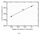
- the Ta 2 O 5 doping concentration-carrier concentration-resistivity curve of samples without annealing in Examples 1-4 are shown in Fig.1 .
- Examples 5-9 correspond to the curve of NbzOs doping concentration-carrier concentration-resistivity, as shown in Figure 3 .
- the present invention draws the doping concentration-carrier concentration curve of the samples annealed in Examples 1-3 as shown in Fig. 2 .
- Figs. 1 and 3 there is a linear relationship between M 2 O 5 doping concentration and carrier concentration, and between M 2 O 5 doping concentration and resistivity.
- the carrier concentration increases linearly and the resistivity decreases linearly with the increase of M 2 O 5 doping concentration before annealing.
- the carrier concentration decreases after annealing.
- the carrier concentration and resistivity of the above Group VB elements doped ⁇ - Ga 2 O 3 single crystal are obtained by the specific experiments of the present invention. Due to the influence of the purity of raw materials, preparation technology and test conditions, the measured carrier concentration and resistivity of the doped crystal will be different from the theoretical value, or there is a situation that cannot be detected. Therefore, the above examples are merely illustrations.
- the carrier concentration of the Group VB element doped ⁇ - Ga 2 O 3 crystalline material can be controlled in the range of 5 ⁇ 10 12 to 7 ⁇ 10 20 /cm 3
- the resistivity can be controlled in the range of 2.0 ⁇ 10 -4 to 1 ⁇ 10 4 ⁇ cm.
- the Hall effect instrument with low resistance module is used to test the resistivity below the limit value of 10 5 ⁇ cm.
- the experiment of the present invention shows that the resistivity of 6N pure ⁇ -Ga 2 O 3 crystal exceeds the test limit after annealing, indicating that the resistivity of 6N pure ⁇ -Ga 2 O 3 crystal exceeds 10 5 ⁇ cm. Therefore, the resistivity of 6N pure ⁇ -Ga 2 O 3 doped with Ta can be controlled to 1 ⁇ 10 4 ⁇ cm, which is 1/1266 of Example 1.
- the carrier concentration in the example is multiplied by 1/1266, 3 ⁇ 10 12 /cm 3 can be obtained, so it is feasible to achieve 5 ⁇ 10 12 /cm 3 carrier concentration in Ta-doped ⁇ -Ga 2 O 3 crystalline material.
- the doping concentration of Ta corresponding to the doping concentration is 10 -7 at%.
- the resistivity can be controlled in the range of 2.0 ⁇ 10 -4 to 1 ⁇ 10 4 ⁇ cm
- the carrier concentration can be controlled in the range of 5 ⁇ 10 12 to 7 ⁇ 10 20 /cm 3 .
- Nb and V may be calculated by the same method.
Landscapes
- Chemical & Material Sciences (AREA)
- Organic Chemistry (AREA)
- Engineering & Computer Science (AREA)
- Crystallography & Structural Chemistry (AREA)
- Materials Engineering (AREA)
- Metallurgy (AREA)
- Inorganic Chemistry (AREA)
- Physics & Mathematics (AREA)
- Thermal Sciences (AREA)
- Crystals, And After-Treatments Of Crystals (AREA)
Description
- The present invention relates to crystalline material of β-Ga2O3 doped with group VB elements and preparation method and application thereof.
- β-Ga2O3 is a direct wide bandgap semiconductor material with a bandgap of approximately 4.8-4.9 eV. The material has many advantages including wide bandgap, fast drift velocity of saturated electrons, high thermal conductivity, high breakdown voltage, and stable chemical properties, and the region from the deep ultraviolet (DUV) to the infrared (IR) is transparent. Compared with traditional transparent conductive materials, the material based on β-Ga2O3 may be used to prepare a new generation of semiconductor optoelectronic devices with shorter wavelength.
- Pure β-Ga2O3 crystals exhibit semi-insulating or weakly n-type conductive. Currently, known major method to improve the n-type conductivity of the β-Ga2O3 crystals is to carry out tetravalent ion (group IV elements) doping, from the fourth main group and the fourth subgroup, which mainly includes doping with ions of Si, Hf, Ge, Sn, Zr, Ti, etc. Taking Si as an example, the main mechanism of improving carrier concentration is as follows:

- The equation shows that the theoretical ultimate ability of free electron supply by Group IV Element doping is about 1:1. With the increase in doping concentration, the difficulty of crystalline crystallization increases, and the improvement of conductivity is limited.
- Among Group IV elements, Si and Sn are the two commonly used for doping. The use of Si for doping with single crystals β-Ga2O3 is disclosed in U.S. Patent Document
US20070166967A1 and Japanese Patent DocumentJP2015083536A US20070166967A1 andJP2015083536A figure 2 of the description). - Sn doped single crystals β-Ga2O3 have been reported in the journal (Thin Solid Films, 2008, 516 (17), 5763-5767). However, due to the high volatility of tin oxides, the Sn content in the obtained crystals is only in ppm level even though 2-10 mol% Sn is added to the raw material. It not only brings great difficulty to control its content and uniformity, but also causes equipment pollution by the volatilization of tin oxide.
- Document
EP2765610 A1 discloses a high-quality Ga2O3 semiconductor element including an n-type β-Ga2O3 substrate; a β-Ga2O3 single crystal film which is formed on the n-type β-Ga2O3 substrate; source electrodes which are formed on the β-Ga2O3 single crystal film; a drain electrode, which is formed on the n-type β-Ga2O3 substrate surface on the reverse side of the β-Ga2O3 single crystal film; n-type contact regions, which are formed in the β-Ga2O3 single crystal film, and have the source electrodes connected thereto, respectively; and a gate electrode, which is formed on the β-Ga2O3 single crystal film with the gate insulating film therebetween. - Document
WO2016/152335 A1 discloses a crystal laminate structure including a β-Ga2O3 based substrate; a β-Ga2O3 based single crystal film formed by epitaxial crystal growth on a primary face of the β-Ga2O3 based substrate and including Cl and a dopant doped in parallel with the crystal growth at a concentration of 1×10¹³ to 5.0×10²⁰ atoms/cm3. - Therefore, how to prepare doped β-Ga2O3 with high conductivity in a simple way has become an important research topic in this field.
- The problem to be solved by the present invention is overcoming the limitation on the degree of improvement in the conductivity of the Group IV elements doped crystalline β-Ga2O3, difficulty in crystallization and harsh process conditions in preparing Group IV element doped crystalline β-Ga2O3, with high conductivity. The present invention provides a class of Group VB element doped β-Ga2O3 crystalline material, preparation method and application thereof. The crystalline material doped with Group VB elements of the present invention exhibits n-type conductive characteristics, and β-Ga2O3 crystalline materials with high conductivity may be prepared by conventional process.
- Generally, doping ions with higher valence state than Ga3+ in crystalline β-Ga2O3 can improve the conductivity to some extent. However, it is generally believed that if the doping ion valence state is too high, the charge is difficult to balance, and it is easy to produce more doping defects. Defects can trap electrons, significantly reduce the number of carriers that can move freely, fail to effectively achieve the purpose of improving the conductivity by doping high valence ions, and seriously affect the application performance of materials. Therefore, currently technologies usually use Group IV elements with one higher valence than Ga3+ to dope β-Ga2O3 crystals, and Group VB elements have not been reported to dope crystals.
- However, through scientific design and experimental verification, the inventor of the present invention has found that certain amount of pentavalent Group VB (M=Nb, Ta, V, etc.) metal ion doped crystalline β-Ga2O3 provides more free electrons than that of the commonly tetravalent ions doping, thus improving the carrier concentration and thereby facilitating the improvement of the conductivity. Moreover, the conductivity of the β-Ga2O3 crystalline material is regulated by the content control of doped element M. The main defect reaction mechanism is as follows:

- As seen from the above equation, the theoretical ultimate ability of free electron supply by doping elements of Group VB can be 1:2, and the improvement in conductivity is significantly greater than that of Group IV elements. Therefore, crystals is obtained at high doping concentration by using conventional process.
- Further, the inventor of the present invention has found that after annealing the crystalline β-Ga2O3 doped with Group VB elements, the oxygen vacancy in the crystal is removed, and the control range of carrier concentration is increased, providing a basis for expanding its application range.
- The present invention solves the above technical problems through the following technical solutions.
- The present invention provides a doped gallium oxide crystalline material, wherein the doped gallium oxide crystalline material is a Group VB element M-doped β-Ga2O3 crystalline material, the doped Group VB element M is vanadium (V), niobium (Nb), tantalum (Ta), or a combination thereof, and the doped gallium oxide crystalline material is adjusted by controlling a doping concentration of the Group VB element M and annealing the doped gallium oxide crystalline material at annealing temperature from 1000 °C to 1200°C for 3-10 hours to have at least one of a resistivity in a range of 2.0x10⁻⁴ to 1×10⁴ Ω·cm and a carrier concentration in the range of 5×10¹² to 7×10²⁰/cm3, wherein a molecular formula of the doped gallium oxide crystalline material is Ga2(1-x)M2xO3, and x is defined as 0.000000001≤x≤0.01.
- The present invention further provides a method for preparing an M-doped β-Ga2O3 crystalline material. The method includes mixing M2O5 and Ga2O3, both the M2O5 and Ga2O3 having a purity of above 4N, in a molar ratio of (0.000000000001-0.01): (0.9999999-0.99) to grow crystals, obtaining an M-doped gallium oxide crystalline material; and annealing the M-doped β-Ga2O3 crystalline material at annealing temperature from 1000 °C to 1200°C for 3-10 hours after crystal growth, wherein the M is a Group VB element, wherein the Group VB element is vanadium (V), niobium (Nb), tantalum (Ta), or a combination thereof.
- The invention is set out in the appended set of claims.
- The present invention provides a Group VB element-doped β-Ga2O3 crystalline material, doped elements M=Nb, Ta, V, etc. The doped crystal belongs to monoclinic crystalline system and the space group is C2/m. The doped β- Ga2O3 crystalline material described has a resistivity in 2.0×10⁻⁴ to 1 ×10⁴ Ω·cm range and/or a carrier concentration ranging from 5×10¹² to 7×10²⁰/cm3.
- In the present invention, the term crystalline material refers to a solid material whose internal structure presents a long range order, including solid crystal and liquid crystal where solid state material is the main component, etc. Among the crystal materials, crystalline material is categorized according to the macroscopic aggregate state and particle diameter of the crystalline particles during the crystallization process to, including, single crystal, thin film, polycrystalline (powder crystal), eutectic, microcrystalline, and nano crystalline, etc. In the present invention, there is no special limitation on the macroscopic existing form of the crystalline material, it can be such as powder, particle, film, etc.
- In the present invention, x is defined as 0.000001≤x≤0.01.
- In the present invention, the M doped β-Ga2O3 crystalline material is preferably M doped β-Ga2O3 crystal, and more preferably, M doped β-Ga2O3 single crystal.
- In the present invention, the resistivity range of M doped β-Ga2O3 crystalline material is preferably from 2.0×10⁻³ to 3.6×10² Ω·cm. If M is Ta, the preferred range is from 4×10⁻³ to 7.9 Ω·cm. If M is Nb, the preferred range is from 5.5×10⁻³ to 36 Ω·cm. If M is V, the preferred range is from 3×10⁻² to 50 Ω·cm.
- In the present invention, the preferred carrier concentration range of M doped β-Ga2O3 crystalline material is from 3.7×10¹⁵ to 6.3×10¹⁹/cm3. If M is Ta, the preferred range is from 3.7×10¹⁵ to 3.0×10¹⁹/cm3. If M is Nb, the preferred range is from 9.55×10¹⁶ to 1.8×10¹⁹/cm3. If M is V, the preferred range is from 5×10¹⁵ to 3.69×10¹⁸/cm3.
- Doping scheme provided by the present invention is obtained by the conventional crystal growth method. According to the conventional method in the field, M2O5 and Ga2O3 with purity above 4N are mixed according to a molar ratio of (0.000000001-0.01) : (0.9999999-0.99) for crystal growth.
- In the present invention, the term purity refers to the mass fraction of M2O5 or Ga2O3 in the sample. Purity 4N means that the mass fraction of M2O5 or Ga2O3 is 99.99%. When the raw material purity of M2O5 or Ga2O3 is lower than the required purity, the conductivity of the final crystalline material is affected due to excessive impurities.
- In the present invention, the purity of M2O5 and Ga2O3 is better than 5N, that is, the mass content of M2O5 or Ga2O3 in the sample is 99.999%. When the M doped β-Ga2O3 crystalline material is M doped β-Ga2O3 single crystal, the purity of Ga2O3 used in the preparation process is better than 6N, that is, the mass content of Ga2O3 in the sample is 99.9999%.
- In the present invention, the M doped β-Ga2O3 crystalline material is annealed to remove defects such as oxygen vacancy in the crystal and increase the control range of the carrier concentration. Conventional annealing temperature and time are used at 1000°C to 1200°C and annealing time of 3-10 hrs.
- In the present invention, M doped β-Ga2O3 crystalline material can contain impurity elements that are unavoidable during the refining process of the raw materials and impurity elements that are inevitably mixed in during the process. Compared with all compositions, the above impurity element content is preferably below 10ppm.
- In the present invention, the crystal growth method and condition used for preparing doped β-Ga2O3 crystalline materials are not specifically limited, which may be conventional crystal growth method and condition in the field. When the doped β-Ga2O3 crystalline material is a single crystal, the melt method commonly used in the field is used to grow the single crystal. Generally, the melt growth method is to introduce the seed crystal into the melt and control the nucleation of the single crystal, and then carry out the phase transition at the phase interface between the seed crystal and the melt to promote the continuous growth of the crystal, including the Czochralski, edge-defined film fed growth, Bridgman-Stockbarger methods, the optical floating zone method, the flame melting method and so on. The optical floating zone method and edge-defined film fed growth method are both simple and efficient methods. The examples of the present invention adopt the optical floating region method.
- Among them, the steps of preparing the M-doped β-Ga2O3 single crystal by the optical floating zone method generally include mixing, rod making, sintering, and crystal growth.
- In the process, the mixing is carried out by a mixing method conventionally used in the art, such as wet mixing. The kind and amount of the solvent to be used in the wet mixing are not particularly limited as long as the M2O5 and Ga2O3 are uniformly mixed and the solvent is easily removed later, and a volatile solvent such as ethanol is generally used. After dispersing and mixing M2O5 and Ga2O3 in a volatile solvent, the solvent is completely volatilized by baking. In order to make the mixing of M2O5 and Ga2O3 more uniform, the wet mixing is also be carried out by a wet ball milling process, which is conventional in the art, for example 12-24 hrs.
- In the process, the rod pressuring can be operated in a manner conventional in the art, and the rod pressuring is generally performed using an isotactic press. Those skilled in the art know that the mixture of M2O5 and Ga2O3 is powdery and can be easily pressed, and can make the pressing uniform. Therefore, if the mixture has agglomeration before pressing, it can be ground into a powder by grinding, such as by ball milling.
- In an embodiment of the present invention, M2O5 having a purity above 4N and Ga2O3 having a purity of 6N are mixed at a molar ratio of (0.000001-0.01): (0.999999-0.99), and wet ball milling is conducted by adding an appropriate amount of absolute ethanol; ball milling time is 12-24hrs, so that M2O5 and Ga2O3 are thoroughly mixed. Then, the mixture obtained is baked at 80-100°C for 3-6 hrs to completely evaporate the ethanol, and then the dried mixture is ball-milled into powdery form for use in rod making by pressurizing.
- In the process, the sintering can be carried out according to the conventional sintering temperature and time in the art to remove moisture in the M2O5 and Ga2O3 mixture, and to solid phase reaction of M2O5 and Ga2O3 to form a polycrystalline material. The sintering temperature is preferably from 1400 to 1600°C, and the sintering time is preferably from 10 to 20 hours. The sintering is generally carried out in a muffle furnace.
- In the process, the crystal growth atmosphere is preferably a vacuum, an inert atmosphere, or an oxidizing atmosphere to ensure the valence state of the Group VB metal M ions. The inert atmosphere may be an inert atmosphere conventional in the art, such as a nitrogen atmosphere or an argon atmosphere; the oxidizing atmosphere may be an oxidizing atmosphere conventional in the art, such as an oxygen atmosphere or an air atmosphere.
- Among them, the preparation of the Group VB metal M-doped β-Ga2O3 single crystal is usually carried out by a melt method. Generally, the β-Ga2O3 crystal is used as a seed crystal, and the melt is formed by melting the sintered M2O5 and Ga2O3 polycrystalline materials, and the melt is gradually cooled and crystallized along the seed crystal to form a single crystal. Specific methods include a floating zone method, edge-defined film fed growth, a temperature gradient method, a Czochralski method, a Bridgman-Stockbarger Method, and the like.
- In one embodiment of the present invention, the growing Group VB metal M-doped β- Ga2O3 single crystal is carried out by a floating zone method, and the following steps are performed. The sintered M2O5 and Ga2O3 polycrystalline rods are loaded into the floating zone furnace as the loading rod, and the Ga2O3crystal in the <010> direction is used as the seed crystal. Firstly, increase the temperature to melt the seed crystal, then contacts the loading rod, adjusts the rotation speed and rotation direction of the rod and the seed crystal, seeding, starts crystal growth. The growth rate of the crystal is 4.5-6 mm/hr, the rotation speed is 8-12 rpm, and the growth atmosphere is an air atmosphere. After the crystal growth is completed, the crystal is pulled from the melting zone, slowly lowered to room temperature, and the crystal is taken out.
- The present invention also provides a Group VB metal M-doped β-Ga2O3 crystalline material obtained by the above preparation method.
- The present invention also provides the use of the M-doped β-Ga2O3 crystalline material on power electronic devices, optoelectronic devices, photo catalysts, or conductive substrates.
- In the present invention, the optoelectronic device comprises a transparent electrode, a solar panel, a light emitting device, a photodetector, a sensor, etc. The conductive substrate includes a substrate material for GaN-based and/or AlN-based material, a substrate material for β- Ga2O3 itself, and the like.
- Based on the common knowledge in the art, the above various preferred conditions can be arbitrarily combined to obtain preferred embodiments of the present invention.
- The reagents and starting materials used in the present invention are commercially available.
- The positive progress and effects achieved by the present invention are:
- (1) In the present invention, the ultimate ability of free electrons supply by doping crystalline β- Ga2O3 with pentavalent Group VB metal ion is 1:2, which is significantly higher than the ability of the +4 valence ion doping to provide free electrons (1:1). Therefore, more free electrons are provided at the same doping concentration, which is more favorable for increasing the carrier concentration and improving the conductivity.
- (2) The present invention adopts pentavalent Group VB metal ion doped crystalline β-Ga2O3, and the conductivity of the β-Ga2O3 crystalline material is controlled by controlling the content of the doping element M. The resistivity of Ta-doped β-Ga2O3 crystalline material is controlled within a range of 2.0×10⁻⁴ to 1 ×10⁴ Ω·cm and the carrier concentration is controlled within a range of 5×10¹² to 7×10²⁰ /cm3; the resistivity of Nb-doped β-Ga2O3 crystalline material is controlled within a range of 2.5×10⁻⁴ to 1×10⁴ Ω·cm, and the carrier concentration is controlled within a range of 5×10¹² to 5.6×10²⁰/cm3; the resistivity of V-doped β-Ga2O3 crystalline material is controlled within a range of 2.0×10⁻⁴ to 1×10⁴ Ω·cm, and the carrier concentration is controlled within a range of 5×10¹² to 7×10²⁰/cm3.
- (3) The Group VB metal-doped β-Ga2O3 crystalline material of the present invention is prepared by a conventional method in the art without expensive raw materials and demanding processes.
- (4) After annealing the Group VB metal doped crystalline β-Ga2O3, the oxygen vacancies in the crystal lattice are removed, and the control range of the carrier concentration increases, thereby providing a basis for its application.
-
-
Figure 1 is a graph showing the relationship between the doping concentration of Ta2O5 and the carrier concentration and resistivity of the Ta-doped β-Ga2O3 as-grown crystal of Example 1-4 in the present invention. -
Figure 2 is a graph showing the relationship between the doping concentration of Ta2O5 after annealing and the carrier concentration of the Ta-doped β-Ga2O3 crystal after annealing of Example 1-3 in the present invention. -
Figure 3 is a graph showing the relationship between the doping concentration of Nb2O5 and the carrier concentration and resistivity of the Nb-doped β-Ga2O3 as-grown crystal of Example 5-9 in the present invention. - The present invention is further illustrated in the following examples, without thereby limiting the present invention to the scope of the examples. The experimental methods in the following examples which do not specify the specific conditions are selected according to conventional methods and conditions, or according to the product specifications.
- In the following examples, the starting materials and reagents used are commercially available.
- A Ta-doped β-Ga2O3 single crystal with a molecular formula of Ga2(1-x)Ta2xO3 (x=0.000001), which belongs to the monoclinic system and has a space group of C2/m, is prepared by the method and specific steps as follows:
- (1) Ingredients: Ga2O3 with a purity above 6N and Ta2O5 with a purity above 4N are weighed according to a molar ratio of 0.999999:0.000001;
- (2) Mixing: put the weighed raw materials into a clean PTFE ball mill jar, put into a highpurity corundum ball, pour the appropriate amount of absolute ethanol, seal, put into a ball mill, and mix for 12 hrs;
- (3) Drying: the ball grinding tank is placed in an oven, baked at 80°C for 6 hrs, the ethanol is completely volatilized, and then placed in a ball mill for 10 minutes to grind the dried bulk material into powder form;
- (4) Rod making: the dried mixed powder is placed in an organic mold and pressed into a material rod by using an isotactic press;
- (5) Sintering: the pressed rod is placed in a muffle furnace and sintered at 1500°C for 10 hrs, the moisture in the raw material is removed, and the Ta2O5 and the Ga2O3 raw material are subjected to solid phase reaction to form a polycrystalline material;
- (6) Crystal growth: the sintered polycrystalline rod is placed in a floating zone furnace as an loading rod, and the Ga2O3 crystal in the <010> direction is placed below as a seed crystal. First, temperature is increased to melt the seed crystal, and then the seed crystal is contacted with the loading rod to reach stabilization and initiate crystal growth. The crystal growth rate is 5 mm/hr, the rotation speed is 10rpm, and the growth atmosphere is air atmosphere. After the crystal growth is completed, stop the dropping of the loading rod, and cause the gradual separation of the melting zone by naturally lowering down the crystal. After about 1 hour, the temperature slowly drops to room temperature, and the crystal is taken out. The as-grown crystal is intact with even color and no cracking;
- (7) Annealing: The resulting as-grown crystals are annealed at 1000°C for 3 hrs.
- A Ta-doped β-Ga2O3 single crystal with a molecular formula of Ga2(1-x)Ta2xO3 (x=0.00005), which belongs to the monoclinic system and has a space group of C2/m, is prepared by the same steps and conditions as in Example 1, except that the doping concentration of Ta2O5 in step (1) is different, and the molar ratio of Ga2O3 to Ta2O5 is 0.99995:0.00005.
- A Ta-doped β- Ga2O3 single crystal with a molecular formula of Ga2(1-x)Ta2xO3 (x=0.001), which belongs to the monoclinic system and has a space group of C2/m, is prepared by the same steps and conditions as in Example 1, except that the doping concentration of Ta2O5 in step (1) is different, and the molar ratio of Ga2O3 to Ta2O5 is 0.999:0.001. Additionally, no annealing operation is performed.
- A Ta-doped β- Ga2O3 single crystal with a molecular formula of Ga2(1-x)Ta2xO3(x=0.01), which belongs to the monoclinic system and has a space group of C2/m, is prepared by the same steps and conditions as in Example 1, except that the doping concentration of Ta2O5 in step (1) is different, and the molar ratio of Ga2O3 to Ta2O5 is 0.99:0.01. No annealing operation is performed.
- A Nb-doped β-Ga2O3 single crystal with a molecular formula of Ga2(1-x)Nb2xO3 (x=0.000001), which belongs to the monoclinic system and has a space group of C2/m, is prepared by the same steps and conditions as in Example 1, except that the dopant (Nb2O5) and doping concentration of Nb2O5 in step (1) are different. The preparation steps and conditions are the same as those in example 1.
- A Nb-doped β-Ga2O3 single crystal with a molecular formula of Ga2(1-x)Nb2xO3 (x=0.00001), which belongs to the monoclinic system and has a space group of C2/m, is prepared by the same steps and conditions as in Example 1, except that the dopant (Nb2O5) and doping concentration of Nb2O5 in step (1) are different. The preparation steps and conditions are the same as those in example 1.
- A Nb-doped β-Ga2O3 single crystal with a molecular formula of Ga2(1-x)Nb2xO3 (x=0.0001), which belongs to the monoclinic system and has a space group of C2/m, is prepared by the same steps and conditions as in Example 1, except that the dopant (Nb2O5) and doping concentration of Nb2O5 in step (1) are different. The preparation steps and conditions are the same as those in example 1. No annealing operation is performed.
- A Nb-doped β-Ga2O3 single crystal with a molecular formula of Ga2(1-x)Nb2xO3 (x=0.002), which belongs to the monoclinic system and has a space group of C2/m, is prepared by the same steps and conditions as in Example 1, except that the dopant (Nb2O5) and doping concentration of Nb2O5 in step (1) are different. The preparation steps and conditions are the same as those in example 1. No annealing operation is performed.
- A Nb-doped β-Ga2O3 single crystal with a molecular formula of Ga2(1-x)Nb2xO3 (x=0.008), which belongs to the monoclinic system and has a space group of C2/m, is prepared by the same steps and conditions as in Example 1, except that the dopant (Nb2O5) and doping concentration of Nb2O5 in step (1) are different. The preparation steps and conditions are the same as those in example 1. No annealing operation is performed.
- A V-doped β-Ga2O3 single crystal with a molecular formula of Ga2(1-x)V2xO3 (x=0.01), which belongs to the monoclinic system and has a space group of C2/m, is prepared by the same steps and conditions as in Example 1, except that the dopant (V2O5) and doping concentration of V2O5 in step (1) are different. The preparation steps and conditions are the same as those in example 1. No annealing operation is performed.
- A V-doped β-Ga2O3 single crystal with a molecular formula of Ga2(1-x)V2xO3 (x=0.00001), which belongs to the monoclinic system and has a space group of C2/m, is prepared by the same steps and conditions as in Example 1, except that the dopant (V2O5) and doping concentration of V2O5 in step (1) are different. The preparation steps and conditions are the same as those in example 1. No annealing operation is performed.
- A pure β-Ga2O3 single crystal without Ta2O5 doping is prepared by the same steps and conditions as in Example 1.
- The M-doped maple- Ga2O3 single crystals obtained in Examples 1-12 and the pure Ga2O3 single crystal in the comparative example (including the as-grown crystal and the annealed crystal) are cut into samples with the size of 5 mm×5 mm×0.3 mm. Four Indium electrodes are fabricated on four corners of each of the samples and Hall measurements are taken. The measurement results show that all doped crystal samples of Examples 1-12 show n-type conductivity, and detail results of carrier concentration and resistivity of samples in Examples 1-4, 7-12 and Contrastive Example are as shown in Table 1.
Table 1. Carrier concentration and resistivity of different examples in Examples 1-13 and Comparative Example Samples Dopants carrier concentration (/cm3) Resistivity (Ω·cm) as-grown after annealing as-grown after annealing Example 1 Ta=0.000001 7.12×10¹⁷ 3.7×10¹⁵ 0.13 7.9 Example2 Ta=0.00005 1.44×10¹⁸ 5.4×10¹⁶ 0.04 0.86 Examples Ta=0.001 6.3×10¹⁸ 1.7×10¹⁷ 0.02 - Example4 Ta=0.01 3.0×10¹⁹ - 0.004 - Example5 Nb=0.000001 2.014×10¹⁸ 9.554×10¹⁶ 0.07746 36.63 Example6 Nb=0.00001 7.484×10¹⁸ 2.613×10¹⁷ 0.01584 2.065 Example7 Nb=0.0001 1.596×10¹⁸ - 0.09291 - Examples Nb=0.002 8.818×10¹⁸ - 0.009181 - Example9 Nb=0.008 1.812×10¹⁹ - 0.005523 - Example 10 V=0.01 3.69×10¹⁸ 0.03 Example 11 V=0.000001 2.68×10¹⁷ - 0.54 - Contrastive example - 3.96×10¹⁴ exceeding limit of detection 67 exceeding limit of detection - According to the data from Table 1, the pure as-grown crystal of β-Ga2O3 is almost insulated after annealing. Compared with the pure β-Ga2O3 as-grown crystal, the carrier concentration and conductivity of β-Ga2O3 single crystal doped with Group VB elements increase significantly, and the carrier concentration increase at least 103 times and the resistivity decrease at least 500 times, indicating that M metal ions have been successfully doped into the lattice of β-Ga2O3 and achieve desired control effect.
- Further, in order to study the relationship between different doping concentrations and carrier concentration or resistivity in the as-grown crystal, the Ta2O5 doping concentration-carrier concentration-resistivity curve of samples without annealing in Examples 1-4 are shown in
Fig.1 . Examples 5-9 correspond to the curve of NbzOs doping concentration-carrier concentration-resistivity, as shown inFigure 3 . In addition, in order to study the relationship between the doping concentration of Ta2O5 and carrier concentration after annealing, the present invention draws the doping concentration-carrier concentration curve of the samples annealed in Examples 1-3 as shown inFig. 2 . - It can be seen from
Figs. 1 and3 that there is a linear relationship between M2O5 doping concentration and carrier concentration, and between M2O5 doping concentration and resistivity. Within the doping concentration range of the present invention, the carrier concentration increases linearly and the resistivity decreases linearly with the increase of M2O5 doping concentration before annealing. As shown inFigure 2 , the carrier concentration decreases after annealing. - It should be noted that the carrier concentration and resistivity of the above Group VB elements doped β- Ga2O3 single crystal are obtained by the specific experiments of the present invention. Due to the influence of the purity of raw materials, preparation technology and test conditions, the measured carrier concentration and resistivity of the doped crystal will be different from the theoretical value, or there is a situation that cannot be detected. Therefore, the above examples are merely illustrations. According to the Group VB element doping concentration disclosed by the present invention and the common knowledge in the field, it can be inferred that the carrier concentration of the Group VB element doped β- Ga2O3 crystalline material can be controlled in the range of 5×10¹² to 7×10²⁰/cm3, and the resistivity can be controlled in the range of 2.0×10⁻⁴ to 1×10⁴ Ω·cm. Taking Taas an example, the specific calculation process is as follows.
- According to the experiment of the present invention, the maximum value of Tadoping concentration in the β- Ga2O3 single crystal is 1 at% (i.e. x=0.01).
- The volume of 1 mole β-Ga2O3 is 184.44/5.94cm3=31cm3;
The number of Ta atoms in 1 mole Ta-doped β- Ga2O3 is: 1 ×2×1%×6.023×1023=1.2×10²²; therefore, the theoretical value of carrier concentration of Ta-doped β-Ga2O3 is 2×1.2×1022/31=7.7×1020/cm3. - The Hall effect instrument with low resistance module is used to test the resistivity below the limit value of 105 Ω·cm. The experiment of the present invention shows that the resistivity of 6N pure β-Ga2O3 crystal exceeds the test limit after annealing, indicating that the resistivity of 6N pure β-Ga2O3 crystal exceeds 105 Ω·cm. Therefore, the resistivity of 6N pure β-Ga2O3 doped with Ta can be controlled to 1×10⁴ Ω·cm, which is 1/1266 of Example 1. The carrier concentration in the example is multiplied by 1/1266, 3×10¹²/cm3 can be obtained, so it is feasible to achieve 5×10¹²/cm3 carrier concentration in Ta-doped β-Ga2O3 crystalline material.
- The doping concentration of Ta corresponding to the doping concentration is 10-7 at%.
- Therefore, the amount of Ta doping in Ta-doped β-Ga2O3 crystalline materials can be controlled in the range of x=0.000000001 to 0.01, the resistivity can be controlled in the range of 2.0×10⁻⁴ to 1×10⁴ Ω·cm, and the carrier concentration can be controlled in the range of 5×10¹² to 7×10²⁰ /cm3.
- Other doped elements including Nb and V may be calculated by the same method.
- The examples of the present invention are described above. The scope of protection advocated by the present invention shall prevail as described in the claims.
Claims (14)
- A doped gallium oxide crystalline material, wherein the doped gallium oxide crystalline material is a Group VB element M-doped β-Ga2O3 crystalline material, the doped Group VB element M is vanadium (V), niobium (Nb), tantalum (Ta), or a combination thereof, and the doped gallium oxide crystalline material is adjusted by controlling a doping concentration of the Group VB element M and annealing the doped gallium oxide crystalline material at annealing temperature from 1000 °C to 1200°C for 3-10 hours to have at least one of a resistivity in a range of 2.0×10⁻⁴ to 1×10⁴ Ω·cm and a carrier concentration in the range of 5×10¹² to 7×10²⁰/cm3, wherein a molecular formula of the doped gallium oxide crystalline material is Ga2(1-x)M2xO3., and x is defined as 0.000000001≤x≤0.01.
- The doped gallium oxide crystalline material of claim 1, wherein the gallium oxide is a monoclinic β-Ga2O3 crystal with a space group of C2/m.
- The doped gallium oxide crystalline material of claim 1, wherein x is defined as 0.0000011≤x≤0.01.
- The doped gallium oxide crystalline material of claim 1 or 2, wherein the doped gallium oxide crystalline material is Ta-doped β-Ga2O3 crystalline material, and the Ta-doped β-Ga2O3 crystalline material has at least one of a resistivity in a range of 2.0×10⁻⁴ to 1 ×10⁴ Ω·cm and a carrier concentration in a range of 5×10¹² to 7×10²⁰/cm3.
- The doped gallium oxide crystalline material of claim 4, wherein the molecular formula of the Ta-doped β-Ga2O3 crystalline material is Ga2(1-x)Ta2xO3, 0.000001≤x≤0.01.
- The doped gallium oxide crystalline material of claim 1 or 2, wherein the doped gallium oxide crystalline material is a Nb-doped β-Ga2O3 crystalline material having at least one of a resistivity in a range of 2.5×10⁻⁴ to 1 ×10⁴Ω·cm and a carrier concentration in a range of 5×10¹² to 5.6×10²⁰/cm3.
- The doped gallium oxide crystalline material of claim 6, wherein the molecular formula of the Nb-doped β-Ga2O3 crystalline material is Ga2(1-x)Nb2xO3, 0.000001≤x≤0.008.
- The doped gallium oxide crystalline material of claim 1 or 2, wherein the doped gallium oxide crystalline material is V-doped β-Ga2O3 crystalline material having at least one of a resistivity in a range of 2.0×10⁻⁴ to 1×10⁴ Ω·cm and a carrier concentration in a range of 5×10¹² to 7×10²⁰/cm3.
- The doped gallium oxide crystalline material of claim 8, wherein the molecular formula of the V-doped β-Ga2O3 crystalline material is Ga2(1-x)V2xO3. 0.000001≤x≤0.01.
- The doped gallium oxide crystalline material of claim 9, wherein the V-doped β-Ga2O3 crystalline material is V doped β-Ga2O3 crystal;
the V-doped β-Ga2O3 crystalline material has at least one of a resistivity in a range of 2.0×10⁻³ to 3.6×10² Ω·cm and carrier concentration in a range of 3.7×10¹⁵ to 6.3×10¹⁹/cm3. - The doped gallium oxide crystalline material of claim 10, wherein the V-doped β-Ga2O3 crystalline material is V-doped β-Ga2O3 single crystal;
the V-doped β-Ga2O3 crystalline material has at least one of a resistivity in a range of 3×10⁻² to 50 Ω·cm and a carrier concentration in a range of 5×10¹⁵ to 3.69×10¹⁸/cm3. - A method for preparing an M-doped β-Ga2O3 crystalline material, comprising:mixing M2O5 and Ga2O3, both the M2O5 and Ga2O3 having a purity of above 4N, in a molar ratio of (0.000000000001-0.01): (0.9999999-0.99) to grow crystals, obtaining an M-doped gallium oxide crystalline material, andannealing the M-doped β-Ga2O3 crystalline material at annealing temperature from 1000 °C to 1200°C for 3-10 hours after crystal growth,wherein the M is a Group VB element, wherein the Group VB element is vanadium (V), niobium (Nb), tantalum (Ta), or a combination thereof.
- The method of claim 12, wherein the purity of M2O5 and Ga2O3 are both higher than 5N;when the M-doped β-Ga2O3 crystalline material is an M-doped β-Ga2O3 single crystal, the purity of Ga2O3 used in preparing process is higher than 6N; andthe molar ratio of M2O5 and Ga2O3 is in a range of (0.000001-0.01):(0.999999-0.99).
- The method of claim 12, wherein when the M-doped β-Ga2O3 crystalline material is an M-doped β-Ga2O3 single crystal, the single crystal is grown by a melt method chosen from any one of an edge defined film-fed growth (EFG) method, Czochralski method, floating zone method, or Bridgman method.
Applications Claiming Priority (3)
| Application Number | Priority Date | Filing Date | Title |
|---|---|---|---|
| CN201710061035.XA CN108342775B (en) | 2017-01-25 | 2017-01-25 | Tantalum-doped beta gallium oxide crystalline material and preparation method and application thereof |
| CN201710124917.6A CN108531989A (en) | 2017-03-03 | 2017-03-03 | Doped gallium oxide crystal and preparation method thereof |
| PCT/CN2018/074058 WO2018137673A1 (en) | 2017-01-25 | 2018-01-24 | Gallium oxide-doped crystalline material, preparation method and application thereof |
Publications (3)
| Publication Number | Publication Date |
|---|---|
| EP3572561A1 EP3572561A1 (en) | 2019-11-27 |
| EP3572561A4 EP3572561A4 (en) | 2020-01-08 |
| EP3572561B1 true EP3572561B1 (en) | 2023-06-28 |
Family
ID=62979047
Family Applications (1)
| Application Number | Title | Priority Date | Filing Date |
|---|---|---|---|
| EP18744070.6A Active EP3572561B1 (en) | 2017-01-25 | 2018-01-24 | Gallium oxide-doped crystalline material, preparation method and application thereof |
Country Status (7)
| Country | Link |
|---|---|
| US (1) | US11098416B2 (en) |
| EP (1) | EP3572561B1 (en) |
| JP (1) | JP6956189B2 (en) |
| KR (1) | KR102414621B1 (en) |
| CN (1) | CN110325671A (en) |
| SG (1) | SG11202000619WA (en) |
| WO (1) | WO2018137673A1 (en) |
Families Citing this family (13)
| Publication number | Priority date | Publication date | Assignee | Title |
|---|---|---|---|---|
| FR3085535B1 (en) * | 2019-04-17 | 2021-02-12 | Hosseini Teherani Ferechteh | A method of manufacturing p-type gallium oxide by intrinsic doping, the resulting thin film of gallium oxide and its use |
| EP3981023A4 (en) * | 2019-06-06 | 2023-06-28 | Bowling Green State University | METHOD FOR TUNING ELECTRICAL PROPERTIES OF OXIDE SEMICONDUCTORS AND THE DEVELOPMENT OF HIGHLY CONDUCTIVE P-TYPE AND N-TYPE Ga²O³ |
| CN111077560B (en) * | 2019-12-03 | 2022-12-16 | 同济大学 | An X-ray and Gamma-ray detector based on magnesium-doped gallium oxide single crystal |
| CN112086344B (en) * | 2020-09-22 | 2022-12-20 | 中山大学 | A preparation method of aluminum gallium oxide/gallium oxide heterojunction thin film and its application in vacuum ultraviolet detection |
| US11462402B2 (en) * | 2020-10-21 | 2022-10-04 | Cornell University | Suboxide molecular-beam epitaxy and related structures |
| JP7637544B2 (en) * | 2021-03-25 | 2025-02-28 | Tdk株式会社 | Crystal manufacturing method, crystal manufacturing apparatus, and single crystal |
| CN114086254B (en) * | 2021-10-12 | 2022-11-11 | 杭州富加镓业科技有限公司 | Ga 2 O 3 Single crystal and method for producing the same |
| CN114134561A (en) * | 2021-12-07 | 2022-03-04 | 杭州富加镓业科技有限公司 | Crystal growth thermal field dynamic reflecting screen adjusting method |
| CN114408970B (en) * | 2022-01-25 | 2023-07-18 | 重庆邮电大学 | A method for preparing hollow mesoporous carbon-doped gallium trioxide nanospheres and products thereof |
| WO2024053010A1 (en) * | 2022-09-07 | 2024-03-14 | 住友電気工業株式会社 | High-purity digallium trioxide, and method for producing same |
| EP4726083A1 (en) * | 2023-06-07 | 2026-04-15 | Sumitomo Electric Industries, Ltd. | Digallium trioxide single crystal substrate, method for producing digallium trioxide single crystal, and method for producing digallium trioxide single crystal substrate |
| KR102807522B1 (en) * | 2023-09-21 | 2025-05-15 | 동의대학교 산학협력단 | Method of manufacturing single crystal using doped pellet and single crystal manufactured thereby |
| CN121575482A (en) * | 2025-12-01 | 2026-02-27 | 北京镓创科技有限公司 | A method for preparing tin-doped gallium oxide single crystal material |
Family Cites Families (11)
| Publication number | Priority date | Publication date | Assignee | Title |
|---|---|---|---|---|
| JP4083396B2 (en) * | 2000-07-10 | 2008-04-30 | 独立行政法人科学技術振興機構 | Ultraviolet transparent conductive film and manufacturing method thereof |
| CN1266032C (en) * | 2000-10-17 | 2006-07-26 | 夏普株式会社 | Oxide material, method for producing oxide thin film, and device using same |
| JP4630986B2 (en) * | 2003-02-24 | 2011-02-09 | 学校法人早稲田大学 | β-Ga2O3-based single crystal growth method |
| CA2517024C (en) * | 2003-02-24 | 2009-12-01 | Waseda University | .beta.-ga2o3 single crystal growing method, thin-film single crystal growing method, ga2o3 light-emitting device, and its manufacturing method |
| JP2005235961A (en) | 2004-02-18 | 2005-09-02 | Univ Waseda | Method for controlling conductivity of Ga2O3-based single crystal |
| CN102431977B (en) * | 2011-09-05 | 2013-02-13 | 吉林大学 | Method for preparing manganese-doped gallium nitride nano-material |
| WO2013035845A1 (en) * | 2011-09-08 | 2013-03-14 | 株式会社タムラ製作所 | Ga2o3 semiconductor element |
| CN103878010B (en) | 2014-04-15 | 2016-02-17 | 哈尔滨工业大学 | VB race metal ion mixing (Ga 1-xzn x) (N 1-xo x) preparation method of mischcrystal photocatalyst |
| JP2015083536A (en) | 2014-11-04 | 2015-04-30 | 学校法人早稲田大学 | β-Ga2O3 single crystal and light emitting device |
| JP6376600B2 (en) * | 2015-03-20 | 2018-08-22 | 株式会社タムラ製作所 | Method for manufacturing crystal laminated structure |
| CN105239162A (en) * | 2015-08-25 | 2016-01-13 | 中国科学院上海光学精密机械研究所 | Aluminum oxide-gallium oxide mixed-crystal material for wide-band-gap semiconductors |
-
2018
- 2018-01-24 CN CN201880004978.1A patent/CN110325671A/en active Pending
- 2018-01-24 EP EP18744070.6A patent/EP3572561B1/en active Active
- 2018-01-24 JP JP2019537809A patent/JP6956189B2/en active Active
- 2018-01-24 SG SG11202000619WA patent/SG11202000619WA/en unknown
- 2018-01-24 WO PCT/CN2018/074058 patent/WO2018137673A1/en not_active Ceased
- 2018-01-24 KR KR1020197025013A patent/KR102414621B1/en active Active
-
2019
- 2019-07-10 US US16/508,211 patent/US11098416B2/en active Active
Also Published As
| Publication number | Publication date |
|---|---|
| WO2018137673A1 (en) | 2018-08-02 |
| KR20200002789A (en) | 2020-01-08 |
| CN110325671A (en) | 2019-10-11 |
| EP3572561A1 (en) | 2019-11-27 |
| KR102414621B1 (en) | 2022-06-30 |
| US20190352798A1 (en) | 2019-11-21 |
| JP6956189B2 (en) | 2021-11-02 |
| JP2020505305A (en) | 2020-02-20 |
| SG11202000619WA (en) | 2020-02-27 |
| EP3572561A4 (en) | 2020-01-08 |
| US11098416B2 (en) | 2021-08-24 |
Similar Documents
| Publication | Publication Date | Title |
|---|---|---|
| US11098416B2 (en) | Doped gallium oxide crystalline material and preparation method and application thereof | |
| Gomez et al. | Gallium-doped ZnO thin films deposited by chemical spray | |
| US9768316B2 (en) | Oxide semiconductor thin film and thin film transistor | |
| Fang et al. | Influence of annealing temperature on the structural and optical properties of Mg–Al co-doped ZnO thin films prepared via sol–gel method | |
| JP6289693B2 (en) | Crystalline oxide semiconductor thin film, method for producing crystalline oxide semiconductor thin film, and thin film transistor | |
| JP2011001249A (en) | Igzo-based oxide material and method for producing igzo-based oxide material | |
| Benelmadjat et al. | Fabrication and characterization of pure and Sn/Sb-doped ZnO thin films deposited by sol–gel method | |
| CN101037795A (en) | Sb doped P-type ZnO crystal film and preparation method thereof | |
| CN101931009A (en) | Thin film transistor and method of manufacturing thin film transistor | |
| Ji et al. | Fabrication and characterization of p-type ZnO films by pyrolysis of zinc-acetate–ammonia solution | |
| Peiteado et al. | Microstructural development of tin-doped ZnO bulk ceramics | |
| CN108342775B (en) | Tantalum-doped beta gallium oxide crystalline material and preparation method and application thereof | |
| WO2019155674A1 (en) | Compound semiconductor and production method therefor | |
| Lu et al. | Defect photoluminescence and structure properties of undoping (InxGa1-x) 2O3 films and their dependence on sputtering pressure | |
| CN1303650C (en) | p-Zn1-XMgXO crystal film and method for making same | |
| CN114836832A (en) | Gallium oxide-doped crystal and preparation method thereof | |
| CN111470528A (en) | Tin-containing semiconductor material and preparation method thereof | |
| KR101672346B1 (en) | Method for designing transparent conductive material and method for producing single crystal of antimony doped barium tin oxide | |
| JP6635366B2 (en) | Piezoelectric material, manufacturing method thereof, piezoelectric element and combustion pressure sensor | |
| CN103031597A (en) | The method of growing p-ZnO film by Na-Be co-doping | |
| CN100406620C (en) | Li-doped p-Zn1-xMgxO crystal film and method for preparing same | |
| Balaprakash et al. | Effect of aluminum doping on the structural, morphological, electrical and optical properties of ZnO thin films prepared by sol-gel dip coating | |
| Lin et al. | Growth and characterization of Yb: BaWO4 single crystal | |
| CN1240883C (en) | Method for preparing p-type Zn1-XMgXO crystal film | |
| Wang et al. | Obtainable p-type ZnO film doped with Li by sol-gel method |
Legal Events
| Date | Code | Title | Description |
|---|---|---|---|
| STAA | Information on the status of an ep patent application or granted ep patent |
Free format text: STATUS: THE INTERNATIONAL PUBLICATION HAS BEEN MADE |
|
| PUAI | Public reference made under article 153(3) epc to a published international application that has entered the european phase |
Free format text: ORIGINAL CODE: 0009012 |
|
| STAA | Information on the status of an ep patent application or granted ep patent |
Free format text: STATUS: REQUEST FOR EXAMINATION WAS MADE |
|
| 17P | Request for examination filed |
Effective date: 20190823 |
|
| AK | Designated contracting states |
Kind code of ref document: A1 Designated state(s): AL AT BE BG CH CY CZ DE DK EE ES FI FR GB GR HR HU IE IS IT LI LT LU LV MC MK MT NL NO PL PT RO RS SE SI SK SM TR |
|
| AX | Request for extension of the european patent |
Extension state: BA ME |
|
| A4 | Supplementary search report drawn up and despatched |
Effective date: 20191210 |
|
| RIC1 | Information provided on ipc code assigned before grant |
Ipc: H01L 31/032 20060101ALI20191204BHEP Ipc: C30B 13/00 20060101ALI20191204BHEP Ipc: C30B 15/00 20060101ALI20191204BHEP Ipc: C30B 29/16 20060101AFI20191204BHEP Ipc: C30B 13/34 20060101ALI20191204BHEP Ipc: C30B 33/02 20060101ALI20191204BHEP |
|
| RAP1 | Party data changed (applicant data changed or rights of an application transferred) |
Owner name: SHANGHAI INSTITUTE OF OPTICS AND FINE MECHANICS CH Owner name: NANJING TONGLI CRYSTAL MATERIALS |
|
| DAV | Request for validation of the european patent (deleted) | ||
| DAX | Request for extension of the european patent (deleted) | ||
| RAP1 | Party data changed (applicant data changed or rights of an application transferred) |
Owner name: SHANGHAI INSTITUTE OF OPTICS AND FINE MECHANICS CHINESE ACADEMY OF SCIENCES Owner name: HANGZHOU INSTITUTE OF OPTICS AND FINE MECHANICS |
|
| STAA | Information on the status of an ep patent application or granted ep patent |
Free format text: STATUS: EXAMINATION IS IN PROGRESS |
|
| 17Q | First examination report despatched |
Effective date: 20220422 |
|
| RAP1 | Party data changed (applicant data changed or rights of an application transferred) |
Owner name: SHANGHAI INSTITUTE OF OPTICS AND FINE MECHANICS CHINESE ACADEMY OF SCIENCES Owner name: HANGZHOU FUJIA GALLIUM TECHNOLOGY CO. LTD. |
|
| RIC1 | Information provided on ipc code assigned before grant |
Ipc: C30B 33/02 20060101ALI20230123BHEP Ipc: C30B 13/34 20060101ALI20230123BHEP Ipc: H01L 31/032 20060101ALI20230123BHEP Ipc: C30B 13/00 20060101ALI20230123BHEP Ipc: C30B 29/16 20060101AFI20230123BHEP |
|
| GRAP | Despatch of communication of intention to grant a patent |
Free format text: ORIGINAL CODE: EPIDOSNIGR1 |
|
| STAA | Information on the status of an ep patent application or granted ep patent |
Free format text: STATUS: GRANT OF PATENT IS INTENDED |
|
| INTG | Intention to grant announced |
Effective date: 20230321 |
|
| GRAS | Grant fee paid |
Free format text: ORIGINAL CODE: EPIDOSNIGR3 |
|
| GRAA | (expected) grant |
Free format text: ORIGINAL CODE: 0009210 |
|
| STAA | Information on the status of an ep patent application or granted ep patent |
Free format text: STATUS: THE PATENT HAS BEEN GRANTED |
|
| AK | Designated contracting states |
Kind code of ref document: B1 Designated state(s): AL AT BE BG CH CY CZ DE DK EE ES FI FR GB GR HR HU IE IS IT LI LT LU LV MC MK MT NL NO PL PT RO RS SE SI SK SM TR |
|
| REG | Reference to a national code |
Ref country code: CH Ref legal event code: EP |
|
| REG | Reference to a national code |
Ref country code: AT Ref legal event code: REF Ref document number: 1582772 Country of ref document: AT Kind code of ref document: T Effective date: 20230715 |
|
| REG | Reference to a national code |
Ref country code: IE Ref legal event code: FG4D |
|
| REG | Reference to a national code |
Ref country code: DE Ref legal event code: R096 Ref document number: 602018052430 Country of ref document: DE |
|
| REG | Reference to a national code |
Ref country code: LT Ref legal event code: MG9D |
|
| PG25 | Lapsed in a contracting state [announced via postgrant information from national office to epo] |
Ref country code: SE Free format text: LAPSE BECAUSE OF FAILURE TO SUBMIT A TRANSLATION OF THE DESCRIPTION OR TO PAY THE FEE WITHIN THE PRESCRIBED TIME-LIMIT Effective date: 20230628 Ref country code: NO Free format text: LAPSE BECAUSE OF FAILURE TO SUBMIT A TRANSLATION OF THE DESCRIPTION OR TO PAY THE FEE WITHIN THE PRESCRIBED TIME-LIMIT Effective date: 20230928 |
|
| REG | Reference to a national code |
Ref country code: AT Ref legal event code: MK05 Ref document number: 1582772 Country of ref document: AT Kind code of ref document: T Effective date: 20230628 |
|
| PG25 | Lapsed in a contracting state [announced via postgrant information from national office to epo] |
Ref country code: RS Free format text: LAPSE BECAUSE OF FAILURE TO SUBMIT A TRANSLATION OF THE DESCRIPTION OR TO PAY THE FEE WITHIN THE PRESCRIBED TIME-LIMIT Effective date: 20230628 Ref country code: NL Free format text: LAPSE BECAUSE OF FAILURE TO SUBMIT A TRANSLATION OF THE DESCRIPTION OR TO PAY THE FEE WITHIN THE PRESCRIBED TIME-LIMIT Effective date: 20230628 Ref country code: LV Free format text: LAPSE BECAUSE OF FAILURE TO SUBMIT A TRANSLATION OF THE DESCRIPTION OR TO PAY THE FEE WITHIN THE PRESCRIBED TIME-LIMIT Effective date: 20230628 Ref country code: LT Free format text: LAPSE BECAUSE OF FAILURE TO SUBMIT A TRANSLATION OF THE DESCRIPTION OR TO PAY THE FEE WITHIN THE PRESCRIBED TIME-LIMIT Effective date: 20230628 Ref country code: HR Free format text: LAPSE BECAUSE OF FAILURE TO SUBMIT A TRANSLATION OF THE DESCRIPTION OR TO PAY THE FEE WITHIN THE PRESCRIBED TIME-LIMIT Effective date: 20230628 |
|
| PG25 | Lapsed in a contracting state [announced via postgrant information from national office to epo] |
Ref country code: FI Free format text: LAPSE BECAUSE OF FAILURE TO SUBMIT A TRANSLATION OF THE DESCRIPTION OR TO PAY THE FEE WITHIN THE PRESCRIBED TIME-LIMIT Effective date: 20230628 |
|
| PG25 | Lapsed in a contracting state [announced via postgrant information from national office to epo] |
Ref country code: SK Free format text: LAPSE BECAUSE OF FAILURE TO SUBMIT A TRANSLATION OF THE DESCRIPTION OR TO PAY THE FEE WITHIN THE PRESCRIBED TIME-LIMIT Effective date: 20230628 |
|
| PG25 | Lapsed in a contracting state [announced via postgrant information from national office to epo] |
Ref country code: ES Free format text: LAPSE BECAUSE OF FAILURE TO SUBMIT A TRANSLATION OF THE DESCRIPTION OR TO PAY THE FEE WITHIN THE PRESCRIBED TIME-LIMIT Effective date: 20230628 |
|
| PG25 | Lapsed in a contracting state [announced via postgrant information from national office to epo] |
Ref country code: IS Free format text: LAPSE BECAUSE OF FAILURE TO SUBMIT A TRANSLATION OF THE DESCRIPTION OR TO PAY THE FEE WITHIN THE PRESCRIBED TIME-LIMIT Effective date: 20231028 |
|
| PG25 | Lapsed in a contracting state [announced via postgrant information from national office to epo] |
Ref country code: SM Free format text: LAPSE BECAUSE OF FAILURE TO SUBMIT A TRANSLATION OF THE DESCRIPTION OR TO PAY THE FEE WITHIN THE PRESCRIBED TIME-LIMIT Effective date: 20230628 Ref country code: SK Free format text: LAPSE BECAUSE OF FAILURE TO SUBMIT A TRANSLATION OF THE DESCRIPTION OR TO PAY THE FEE WITHIN THE PRESCRIBED TIME-LIMIT Effective date: 20230628 Ref country code: RO Free format text: LAPSE BECAUSE OF FAILURE TO SUBMIT A TRANSLATION OF THE DESCRIPTION OR TO PAY THE FEE WITHIN THE PRESCRIBED TIME-LIMIT Effective date: 20230628 Ref country code: PT Free format text: LAPSE BECAUSE OF FAILURE TO SUBMIT A TRANSLATION OF THE DESCRIPTION OR TO PAY THE FEE WITHIN THE PRESCRIBED TIME-LIMIT Effective date: 20231030 Ref country code: IS Free format text: LAPSE BECAUSE OF FAILURE TO SUBMIT A TRANSLATION OF THE DESCRIPTION OR TO PAY THE FEE WITHIN THE PRESCRIBED TIME-LIMIT Effective date: 20231028 Ref country code: ES Free format text: LAPSE BECAUSE OF FAILURE TO SUBMIT A TRANSLATION OF THE DESCRIPTION OR TO PAY THE FEE WITHIN THE PRESCRIBED TIME-LIMIT Effective date: 20230628 Ref country code: EE Free format text: LAPSE BECAUSE OF FAILURE TO SUBMIT A TRANSLATION OF THE DESCRIPTION OR TO PAY THE FEE WITHIN THE PRESCRIBED TIME-LIMIT Effective date: 20230628 Ref country code: CZ Free format text: LAPSE BECAUSE OF FAILURE TO SUBMIT A TRANSLATION OF THE DESCRIPTION OR TO PAY THE FEE WITHIN THE PRESCRIBED TIME-LIMIT Effective date: 20230628 Ref country code: AT Free format text: LAPSE BECAUSE OF FAILURE TO SUBMIT A TRANSLATION OF THE DESCRIPTION OR TO PAY THE FEE WITHIN THE PRESCRIBED TIME-LIMIT Effective date: 20230628 |
|
| PG25 | Lapsed in a contracting state [announced via postgrant information from national office to epo] |
Ref country code: PL Free format text: LAPSE BECAUSE OF FAILURE TO SUBMIT A TRANSLATION OF THE DESCRIPTION OR TO PAY THE FEE WITHIN THE PRESCRIBED TIME-LIMIT Effective date: 20230628 |
|
| REG | Reference to a national code |
Ref country code: DE Ref legal event code: R097 Ref document number: 602018052430 Country of ref document: DE |
|
| PG25 | Lapsed in a contracting state [announced via postgrant information from national office to epo] |
Ref country code: DK Free format text: LAPSE BECAUSE OF FAILURE TO SUBMIT A TRANSLATION OF THE DESCRIPTION OR TO PAY THE FEE WITHIN THE PRESCRIBED TIME-LIMIT Effective date: 20230628 |
|
| PLBE | No opposition filed within time limit |
Free format text: ORIGINAL CODE: 0009261 |
|
| STAA | Information on the status of an ep patent application or granted ep patent |
Free format text: STATUS: NO OPPOSITION FILED WITHIN TIME LIMIT |
|
| PG25 | Lapsed in a contracting state [announced via postgrant information from national office to epo] |
Ref country code: IT Free format text: LAPSE BECAUSE OF FAILURE TO SUBMIT A TRANSLATION OF THE DESCRIPTION OR TO PAY THE FEE WITHIN THE PRESCRIBED TIME-LIMIT Effective date: 20230628 |
|
| 26N | No opposition filed |
Effective date: 20240402 |
|
| PG25 | Lapsed in a contracting state [announced via postgrant information from national office to epo] |
Ref country code: SI Free format text: LAPSE BECAUSE OF FAILURE TO SUBMIT A TRANSLATION OF THE DESCRIPTION OR TO PAY THE FEE WITHIN THE PRESCRIBED TIME-LIMIT Effective date: 20230628 |
|
| PG25 | Lapsed in a contracting state [announced via postgrant information from national office to epo] |
Ref country code: MC Free format text: LAPSE BECAUSE OF FAILURE TO SUBMIT A TRANSLATION OF THE DESCRIPTION OR TO PAY THE FEE WITHIN THE PRESCRIBED TIME-LIMIT Effective date: 20230628 |
|
| PG25 | Lapsed in a contracting state [announced via postgrant information from national office to epo] |
Ref country code: MC Free format text: LAPSE BECAUSE OF FAILURE TO SUBMIT A TRANSLATION OF THE DESCRIPTION OR TO PAY THE FEE WITHIN THE PRESCRIBED TIME-LIMIT Effective date: 20230628 |
|
| REG | Reference to a national code |
Ref country code: CH Ref legal event code: PL |
|
| PG25 | Lapsed in a contracting state [announced via postgrant information from national office to epo] |
Ref country code: LU Free format text: LAPSE BECAUSE OF NON-PAYMENT OF DUE FEES Effective date: 20240124 |
|
| GBPC | Gb: european patent ceased through non-payment of renewal fee |
Effective date: 20240124 |
|
| PG25 | Lapsed in a contracting state [announced via postgrant information from national office to epo] |
Ref country code: LU Free format text: LAPSE BECAUSE OF NON-PAYMENT OF DUE FEES Effective date: 20240124 |
|
| PG25 | Lapsed in a contracting state [announced via postgrant information from national office to epo] |
Ref country code: GB Free format text: LAPSE BECAUSE OF NON-PAYMENT OF DUE FEES Effective date: 20240124 |
|
| PG25 | Lapsed in a contracting state [announced via postgrant information from national office to epo] |
Ref country code: BE Free format text: LAPSE BECAUSE OF NON-PAYMENT OF DUE FEES Effective date: 20240131 |
|
| PG25 | Lapsed in a contracting state [announced via postgrant information from national office to epo] |
Ref country code: CH Free format text: LAPSE BECAUSE OF NON-PAYMENT OF DUE FEES Effective date: 20240131 |
|
| PG25 | Lapsed in a contracting state [announced via postgrant information from national office to epo] |
Ref country code: GB Free format text: LAPSE BECAUSE OF NON-PAYMENT OF DUE FEES Effective date: 20240124 Ref country code: CH Free format text: LAPSE BECAUSE OF NON-PAYMENT OF DUE FEES Effective date: 20240131 Ref country code: BE Free format text: LAPSE BECAUSE OF NON-PAYMENT OF DUE FEES Effective date: 20240131 |
|
| REG | Reference to a national code |
Ref country code: BE Ref legal event code: MM Effective date: 20240131 |
|
| PG25 | Lapsed in a contracting state [announced via postgrant information from national office to epo] |
Ref country code: BG Free format text: LAPSE BECAUSE OF FAILURE TO SUBMIT A TRANSLATION OF THE DESCRIPTION OR TO PAY THE FEE WITHIN THE PRESCRIBED TIME-LIMIT Effective date: 20230628 |
|
| PG25 | Lapsed in a contracting state [announced via postgrant information from national office to epo] |
Ref country code: BG Free format text: LAPSE BECAUSE OF FAILURE TO SUBMIT A TRANSLATION OF THE DESCRIPTION OR TO PAY THE FEE WITHIN THE PRESCRIBED TIME-LIMIT Effective date: 20230628 |
|
| PG25 | Lapsed in a contracting state [announced via postgrant information from national office to epo] |
Ref country code: IE Free format text: LAPSE BECAUSE OF NON-PAYMENT OF DUE FEES Effective date: 20240124 |
|
| PG25 | Lapsed in a contracting state [announced via postgrant information from national office to epo] |
Ref country code: IE Free format text: LAPSE BECAUSE OF NON-PAYMENT OF DUE FEES Effective date: 20240124 |
|
| PG25 | Lapsed in a contracting state [announced via postgrant information from national office to epo] |
Ref country code: CY Free format text: LAPSE BECAUSE OF FAILURE TO SUBMIT A TRANSLATION OF THE DESCRIPTION OR TO PAY THE FEE WITHIN THE PRESCRIBED TIME-LIMIT; INVALID AB INITIO Effective date: 20180124 |
|
| PG25 | Lapsed in a contracting state [announced via postgrant information from national office to epo] |
Ref country code: HU Free format text: LAPSE BECAUSE OF FAILURE TO SUBMIT A TRANSLATION OF THE DESCRIPTION OR TO PAY THE FEE WITHIN THE PRESCRIBED TIME-LIMIT; INVALID AB INITIO Effective date: 20180124 |
|
| PG25 | Lapsed in a contracting state [announced via postgrant information from national office to epo] |
Ref country code: GR Free format text: LAPSE BECAUSE OF FAILURE TO SUBMIT A TRANSLATION OF THE DESCRIPTION OR TO PAY THE FEE WITHIN THE PRESCRIBED TIME-LIMIT; INVALID AB INITIO Effective date: 20180124 |
|
| PG25 | Lapsed in a contracting state [announced via postgrant information from national office to epo] |
Ref country code: TR Free format text: LAPSE BECAUSE OF FAILURE TO SUBMIT A TRANSLATION OF THE DESCRIPTION OR TO PAY THE FEE WITHIN THE PRESCRIBED TIME-LIMIT Effective date: 20230628 |
|
| PGFP | Annual fee paid to national office [announced via postgrant information from national office to epo] |
Ref country code: DE Payment date: 20260128 Year of fee payment: 9 |
|
| PGFP | Annual fee paid to national office [announced via postgrant information from national office to epo] |
Ref country code: FR Payment date: 20260126 Year of fee payment: 9 |