EP3570223B1 - Effektive quanten-ram-architektur für eine quantendatenbank - Google Patents
Effektive quanten-ram-architektur für eine quantendatenbank Download PDFInfo
- Publication number
- EP3570223B1 EP3570223B1 EP19174639.5A EP19174639A EP3570223B1 EP 3570223 B1 EP3570223 B1 EP 3570223B1 EP 19174639 A EP19174639 A EP 19174639A EP 3570223 B1 EP3570223 B1 EP 3570223B1
- Authority
- EP
- European Patent Office
- Prior art keywords
- quantum
- state
- qubit
- bus
- bit
- Prior art date
- Legal status (The legal status is an assumption and is not a legal conclusion. Google has not performed a legal analysis and makes no representation as to the accuracy of the status listed.)
- Active
Links
Images


Classifications
-
- G—PHYSICS
- G06—COMPUTING OR CALCULATING; COUNTING
- G06N—COMPUTING ARRANGEMENTS BASED ON SPECIFIC COMPUTATIONAL MODELS
- G06N10/00—Quantum computing, i.e. information processing based on quantum-mechanical phenomena
- G06N10/40—Physical realisations or architectures of quantum processors or components for manipulating qubits, e.g. qubit coupling or qubit control
-
- G—PHYSICS
- G06—COMPUTING OR CALCULATING; COUNTING
- G06F—ELECTRIC DIGITAL DATA PROCESSING
- G06F16/00—Information retrieval; Database structures therefor; File system structures therefor
- G06F16/20—Information retrieval; Database structures therefor; File system structures therefor of structured data, e.g. relational data
- G06F16/22—Indexing; Data structures therefor; Storage structures
-
- G—PHYSICS
- G06—COMPUTING OR CALCULATING; COUNTING
- G06F—ELECTRIC DIGITAL DATA PROCESSING
- G06F16/00—Information retrieval; Database structures therefor; File system structures therefor
- G06F16/20—Information retrieval; Database structures therefor; File system structures therefor of structured data, e.g. relational data
- G06F16/24—Querying
- G06F16/245—Query processing
-
- G—PHYSICS
- G06—COMPUTING OR CALCULATING; COUNTING
- G06F—ELECTRIC DIGITAL DATA PROCESSING
- G06F16/00—Information retrieval; Database structures therefor; File system structures therefor
- G06F16/90—Details of database functions independent of the retrieved data types
- G06F16/901—Indexing; Data structures therefor; Storage structures
-
- G—PHYSICS
- G06—COMPUTING OR CALCULATING; COUNTING
- G06F—ELECTRIC DIGITAL DATA PROCESSING
- G06F3/00—Input arrangements for transferring data to be processed into a form capable of being handled by the computer; Output arrangements for transferring data from processing unit to output unit, e.g. interface arrangements
- G06F3/06—Digital input from, or digital output to, record carriers, e.g. RAID, emulated record carriers or networked record carriers
- G06F3/0601—Interfaces specially adapted for storage systems
- G06F3/0602—Interfaces specially adapted for storage systems specifically adapted to achieve a particular effect
- G06F3/0604—Improving or facilitating administration, e.g. storage management
-
- G—PHYSICS
- G06—COMPUTING OR CALCULATING; COUNTING
- G06F—ELECTRIC DIGITAL DATA PROCESSING
- G06F3/00—Input arrangements for transferring data to be processed into a form capable of being handled by the computer; Output arrangements for transferring data from processing unit to output unit, e.g. interface arrangements
- G06F3/06—Digital input from, or digital output to, record carriers, e.g. RAID, emulated record carriers or networked record carriers
- G06F3/0601—Interfaces specially adapted for storage systems
- G06F3/0628—Interfaces specially adapted for storage systems making use of a particular technique
- G06F3/0655—Vertical data movement, i.e. input-output transfer; data movement between one or more hosts and one or more storage devices
- G06F3/0659—Command handling arrangements, e.g. command buffers, queues, command scheduling
-
- G—PHYSICS
- G06—COMPUTING OR CALCULATING; COUNTING
- G06F—ELECTRIC DIGITAL DATA PROCESSING
- G06F3/00—Input arrangements for transferring data to be processed into a form capable of being handled by the computer; Output arrangements for transferring data from processing unit to output unit, e.g. interface arrangements
- G06F3/06—Digital input from, or digital output to, record carriers, e.g. RAID, emulated record carriers or networked record carriers
- G06F3/0601—Interfaces specially adapted for storage systems
- G06F3/0668—Interfaces specially adapted for storage systems adopting a particular infrastructure
- G06F3/0671—In-line storage system
- G06F3/0673—Single storage device
-
- G—PHYSICS
- G06—COMPUTING OR CALCULATING; COUNTING
- G06N—COMPUTING ARRANGEMENTS BASED ON SPECIFIC COMPUTATIONAL MODELS
- G06N10/00—Quantum computing, i.e. information processing based on quantum-mechanical phenomena
- G06N10/20—Models of quantum computing, e.g. quantum circuits or universal quantum computers
-
- B—PERFORMING OPERATIONS; TRANSPORTING
- B82—NANOTECHNOLOGY
- B82Y—SPECIFIC USES OR APPLICATIONS OF NANOSTRUCTURES; MEASUREMENT OR ANALYSIS OF NANOSTRUCTURES; MANUFACTURE OR TREATMENT OF NANOSTRUCTURES
- B82Y10/00—Nanotechnology for information processing, storage or transmission, e.g. quantum computing or single electron logic
-
- G—PHYSICS
- G06—COMPUTING OR CALCULATING; COUNTING
- G06N—COMPUTING ARRANGEMENTS BASED ON SPECIFIC COMPUTATIONAL MODELS
- G06N7/00—Computing arrangements based on specific mathematical models
- G06N7/01—Probabilistic graphical models, e.g. probabilistic networks
Definitions
- the present invention relates to the architecture of a quantum computing circuit comprising a quantum RAM device being able to using classical data for quantum computing by inputting the classical data as quantum data, .
- Quantum computing technology is being developed as an efficient way to find answers to difficult problems that require large computations.
- Quantum RAM (QRAM) is required to provide input data for quantum computing, but the effective and efficient architecture and method of implementation are not well developed.
- the quantum RAM can achieve speed-ups of a quantum computer by recording large classical data and providing a quantum computer with the data in quantum superposition. There is a need for effectively recording and superposing classical data using the quantum RAM.
- the device complexity is O(N log N) when the classical information capacity (hereinafter referred to as information capacity) of the QRAM is N, in order to record superposed data on the QRAM in a Flip-Flop QRAM.
- a quantum computing circuit comprising: a quantum RAM device for registering multiple input data in a quantum superposition state, wherein each input data is a string of n bits, and wherein the quantum RAM device includes: a bus comprising a plurality n of bus qubits, each of the n bus qubits corresponding to a bit in the string of n bits; and a register qubit wherein the quantum RAM device is configured, for each input data of the multiple input data, to apply a first controlled-bit-flip gate of the quantum RAM device, for performing controlled-bit-flip transform.
- Quantum computing can be implemented with complexity of O(log N) or polynomial complexity of log N, using the fact that speed can be exponentially improved in some applications using a large parallel process provided by a quantum database by which information can be superposed.
- An object of the present invention is to provide systems such as a quantum computing circuit comprising a quantum RAM device and quantum database, being able to effectively record classical information in accordance with the superposition state of bus qubits arbitrarily provided when classical data are to be loaded as quantum data using an existing Flip-Flop QRAM.
- the controlled rotation gate includes a single qubit unitary gate conditionally adjusting the state of the register qubit corresponding to a target qubit of a tensor product state having all control qubits in
- the single qubit unitary gate may be a rotation gate rotated by a predetermined angle about a predetermined axis on the Bloch sphere.
- the controlled rotation gate may perform rotation corresponding to complex probability amplitude information on the Bloch sphere.
- quantum computing can speed-up by use of quantum superposition of information that allows massive parallel processes, with overall cost of O(log N) in some applications.
- quantum database that provides superposed information of a large classical database.
- the related art that is in association with learning parity with noise inspires that such database can be achieved with simple and systematic architecture of quantum circuits.
- the present invention proposes a new class of quantum database (QDB) architecture and protocol that is equivalent to quantum random access memory (QRAM) with an application of classical information.
- QDB quantum database
- This QDB model can be also a good model for classical-to-quantum interface (CQI) and quantum-to-classical interface (QCI).
- Such a quantum database can be implemented using a QRAM.
- a QRAM model requiring a qubit of O(log N) has been proposed in the related art, it is not suitable because due to cost requirement of O(log N) for classical circuits to control all possible quantum states. If applications of a QRAM are exclusively limited to write and read classical data, a very general QRAM architecture in which a quantum circuit cost is O(log N) similar to classical methods can be derived.
- QRAM design for a QDB is addressed in the description of the present invention to obtain a quantum database for reading, writing, and handling classical information with a quantum computing circuit.
- the QDB is configured to be produced using a QRAM, the QRAM understood as a computation register, in which, for example, the data may be modified and updated as a result of computation.
- the QDB can register and store classical data on the QRAM as quantum superposition and can also register and store a quantum process for a query.
- the QDB can store, register, correct, delete, and edit data in response to queries on the basis of data and query processes stored and registered in this way.
- a classical query can be taken by only one at a time, while a quantum query can be taken at a time as quantum superposition through a multiple quantum query type.
- the QRAM state may be modified to represent the result of query.
- the result can be read out by a suitable quantum measurements before final revert process. It is desirable to design the read-out measurement in a way that the measurement may not change the quantum data in the QRAM. In this way, the QRAM of the QDB can be reverted by inversion of the quantum process to restore all the initial quantum data.
- ⁇ ⁇ QBD of a quantum database QDB in which classical data are encoded in a quantum state may be expressed as in [Equation 1].
- d ⁇ l ⁇
- the quantum state of the quantum database may be made through a bus qubit in which the computational basis states of the n + m qubit are in a predetermined superposition state, and a QRAM process QRAM(D) in [Equation 2]. That is, it is possible to process a corresponding quantum query in order to receive a predetermined quantum superposition state corresponding to a plurality of queries as input of the bus qubit and produce a quantum database for the quantum superposition state.
- 0 ⁇ d ⁇ j ⁇ ⁇ d ⁇ l ⁇ j
- a quantum process for constructing the quantum database includes a fundamental quantum unitary computation.
- a QRAM model can be configured using a classically-controlled-bit-flip X and controlled rotation gates (CR, controlled rotations) for controlled probability amplitude adjustment.
- CR controlled rotation gates
- a Hadamard H gate is a single qubit unitary operator, given as [Equation 3].
- the classically-controlled-bit-flip X is also a single qubit unitary computation controlled by a classical control input bit d.
- Two or more qubits may produce a multi-dimensional Hilbert space as a tensor product space.
- a two-qubit state may hold the quantum state information,
- 2 1.
- a controlled rotation gate that is, a controlled rotation (CR) is, in general, a multi-qubit unitary operator, which makes a superposition state having a non-uniform probability amplitude by rotating a resister qubit in which all qubits are coupled to a qubit that is in a
- the sign of a tensor product state is changed into an inverse sign.
- rotation gate (CR y ( ⁇ )) computation of two-qubit controlled R y ( ⁇ ) in which rotation is performed by an angle ⁇ about y-axis on the Bloch sphere is as in [Equation 4].
- the following controlled rotation gates are single qubit unitary gates optionally adjusting the state of a register qubit corresponding to a target qubit of a tensor product state having all control qubits that are in the
- the single qubit unitary gates may be rotated by a predetermined angle about a predetermined axis on the Bloch sphere.
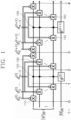
- FIG. 1 is a block diagram of the architecture of a quantum computing circuit for configuring a QRAM (device or system) having a controlled R y ( ⁇ )-rotation gate C n R y ( ⁇ ) in the present invention.
- a method of inputting class information and quantum superposition on a QRAM is described on the basis of FIG. 1 .
- An efficient architecture design of a QRAM model utilizing the controlled R y ( ⁇ )-rotation gate C n R y ( ⁇ ) is proposed in Fig.
- the bus qubit includes states corresponding to each bit of input data and the register qubit includes states given to encode input data into probability amplitude values.
- ⁇ 0 ⁇ l ⁇ d l
- j ⁇ ⁇ means a string in which each bit of the bit string j is bit-flipped.
- the state of [Equation 9] may be obtained by repeating the processes from [Equation 6] to [Equation 8] for a new l + 1-th second data ( d ( l +1) , ⁇ ( l +1) ) using controlled-bit-flip gate X NC 140 and 160 and a controlled rotation gate C n R y (2 ⁇ (l+1) ) 150.
- such a QRAM model may resister 2 n data by quantum superposition that can be simultaneously processed in parallel by quantum computing such as quantum Fourier transform.
- Classical data having a non-uniform weight expressed on the basis of a tensor product may be superposed in complex probability amplitude.
- a gate rotating about another axis may be used rather than the controlled R y ( ⁇ )-gate C n R y ( ⁇ )) rotation.
- R z ( ⁇ )R x (180)R x (- ⁇ ) (x, y and z axes are right angles to each other) instead of R y ( ⁇ ) it is possible to encode e i ⁇ -type complex data with a probability amplitude. That is, a controlled rotation gate that performs rotation corresponding to complex probability amplitude information on the Bloch sphere may be used.
- a QDB for supervised machine learning may be given as superposed learning data
- M denotes the number (natural number) of training data samples and N is the number (natural number) of basic vectors showing x ⁇ k i .
- FIG. 2 An embedding model of the QDB is proposed in FIG. 2 .
- Bit-flip-computation 210 indicated by gray in FIG. 2 is omitted when an actual quantum circuit is implemented, but are left to help understanding.
- the QDB may be used with post-selection that selects 1 as a register qubit measurement.
- quantum computing for i for a data label may be performed simultaneously with quantum data superposition described above and may be correspondingly registered and stored.
- the QRAM described above may process computing such as storing, registering, modifying, and deleting separately for each of a plurality of sets of data.
- FIG. 3 is a method of registering two independent sets of data, in which independent separate computation may be performed on data registered through an n-th qubit when computation that neglects an n + 1-th qubit is performed, and vice versa. Expansion is possible by this method to register two or more sets of data.
- two or more register qubits (only two register qubits are shown in FIG. 3 ) in a
- This is an architecture in which an n + 1-th
- separate computation may be independently processed for input data d ( i ) and d ( j ) of the computing architectures.
- a QRAM using quantum superposition according to the present invention and a QDB using the QRAM may provide new and efficient quantum RAM and quantum database that register data in a way of superposing multiple data input to a qubit of O(log N) and have a protocol about how to express quantum information that can be applied to quantum processing for data computing.
Landscapes
- Engineering & Computer Science (AREA)
- Theoretical Computer Science (AREA)
- Physics & Mathematics (AREA)
- General Physics & Mathematics (AREA)
- General Engineering & Computer Science (AREA)
- Databases & Information Systems (AREA)
- Data Mining & Analysis (AREA)
- Software Systems (AREA)
- Human Computer Interaction (AREA)
- Artificial Intelligence (AREA)
- Computational Mathematics (AREA)
- Condensed Matter Physics & Semiconductors (AREA)
- Evolutionary Computation (AREA)
- Mathematical Analysis (AREA)
- Mathematical Optimization (AREA)
- Pure & Applied Mathematics (AREA)
- Computing Systems (AREA)
- Mathematical Physics (AREA)
- Computational Linguistics (AREA)
- Complex Calculations (AREA)
- Optical Modulation, Optical Deflection, Nonlinear Optics, Optical Demodulation, Optical Logic Elements (AREA)
Claims (4)
- Quantencomputerschaltung, die Folgendes umfasst:
eine Quanten-RAM-Vorrichtung zum Registrieren mehrerer Eingabedaten in einem Quantenüberlagerungszustand, wobei jedes Eingabedatum eine Folge von n Bits ist, und wobei die Quanten-RAM-Vorrichtung Folgendes umfasst:einen Bus, der eine Vielzahl n von Bus-Qubits umfasst, wobei jedes der n Bus-Qubits einem Bit in der Folge von n Bits entspricht; undein Register-Qubit, das zum Codieren jedes Eingangsdatums der mehreren Eingangsdaten in einen Wahrscheinlichkeits-Amplitudenwert gegeben ist; undwobei die Quanten-RAM-Vorrichtung für jedes Eingangsdatum der mehreren Eingangsdaten konfiguriert ist zum:• Anlegen eines ersten gesteuerten Bit-Flip-Gatters (110) der Quanten-RAM-Vorrichtung, um eine gesteuerte Bit-Flip-Transformation an den Bus-Qubits in einem ersten Bus-Qubit-Zustand durchzuführen, um einen zweiten Bus-Qubit-Zustand auszugeben, wobei jedes Bit der Eingangsdaten die Bit-Flip-Transformation seines entsprechenden Bus-Qubits steuert;• Anlegen eines gesteuerten Rotationsgatters (120) der Quanten-RAM-Vorrichtung zur Amplitudenwahrscheinlichkeitsanpassung eines Quantenüberlagerungszustands, der als Tensorprodukt eines Bus-Qubit-Zustands und eines Register-Qubit-Zustands gegeben ist, wobei die Bus-Qubits in dem zweiten Bus-Qubit-Zustand das gesteuerte Rotationsgatter (120) steuern, um das Register-Qubit in einem ersten Register-Qubit-Zustand zu drehen, um einen zweiten Register-Qubit-Zustand und einen dritten Bus-Qubit-Zustand auszugeben, und• Anlegen eines zweiten gesteuerten Bit-Flip-Gatters (130) der Quanten-RAM-Vorrichtung, um eine gesteuerte Bit-Flip-Transformation an den Bus-Qubits im dritten Bus-Qubit-Zustand durchzuführen, um einen vierten Bus-Qubit-Zustand auszugeben, wobei jedes Bit der Eingangsdaten die Bit-Flip-Transformation seines entsprechenden Bus-Qubits steuert. - Quantencomputerschaltung nach Anspruch 1, wobei das gesteuerte Rotationsgatter (120) ein Ein-Qubit-Einheitsgatter enthält, das den Zustand des Register-Qubits entsprechend einem Ziel-Qubit eines Tensorproduktzustands mit allen Steuer-Qubits, die sich in einem |1〉 Zustand befinden, bedingt anpasst.
- Quantencomputerschaltung nach Anspruch 2, wobei das Ein-Qubit-Einheitsgatter ein Rotationsgatter ist, das um einen vorbestimmten Winkel um eine vorbestimmte Achse auf der Bloch-Kugel gedreht ist.
- Quantencomputerschaltung nach Anspruch 1, wobei das gesteuerte Rotationsgatter (120) eine Rotation durchführt, die einer komplexen Wahrscheinlichkeits-Amplitudeninformation auf der Bloch-Sphäre entspricht.
Applications Claiming Priority (1)
| Application Number | Priority Date | Filing Date | Title |
|---|---|---|---|
| KR1020180056581A KR102100368B1 (ko) | 2018-05-17 | 2018-05-17 | 양자 데이터베이스를 위한 효과적 양자 메모리 구조 |
Publications (3)
| Publication Number | Publication Date |
|---|---|
| EP3570223A1 EP3570223A1 (de) | 2019-11-20 |
| EP3570223B1 true EP3570223B1 (de) | 2024-04-24 |
| EP3570223C0 EP3570223C0 (de) | 2024-04-24 |
Family
ID=66554264
Family Applications (1)
| Application Number | Title | Priority Date | Filing Date |
|---|---|---|---|
| EP19174639.5A Active EP3570223B1 (de) | 2018-05-17 | 2019-05-15 | Effektive quanten-ram-architektur für eine quantendatenbank |
Country Status (3)
| Country | Link |
|---|---|
| US (1) | US10824373B2 (de) |
| EP (1) | EP3570223B1 (de) |
| KR (1) | KR102100368B1 (de) |
Families Citing this family (11)
| Publication number | Priority date | Publication date | Assignee | Title |
|---|---|---|---|---|
| KR102100368B1 (ko) | 2018-05-17 | 2020-04-14 | 한국과학기술원 | 양자 데이터베이스를 위한 효과적 양자 메모리 구조 |
| US10901896B2 (en) * | 2018-11-27 | 2021-01-26 | International Business Machines Corporation | Cached result use through quantum gate rewrite |
| CN111291892B (zh) * | 2020-01-17 | 2023-01-17 | 深圳大学 | 一种量子并行搜索方法 |
| CN112000673B (zh) * | 2020-08-31 | 2024-06-14 | 本源量子计算科技(合肥)股份有限公司 | 一种利用量子线路查询交易元素的方法及装置 |
| CN114638366B (zh) * | 2020-11-30 | 2023-08-08 | 本源量子计算科技(合肥)股份有限公司 | 量子地址数据的解析方法、装置、存储介质及电子装置 |
| CN114638368B (zh) * | 2020-11-30 | 2023-08-04 | 本源量子计算科技(合肥)股份有限公司 | 一种用于qram架构的量子线路的构建方法及装置 |
| CN114764549B (zh) * | 2020-12-31 | 2023-04-25 | 合肥本源量子计算科技有限责任公司 | 基于矩阵乘积态的量子线路模拟计算方法、装置 |
| US12468973B2 (en) * | 2021-07-02 | 2025-11-11 | University Of Florida Research Foundation, Incorporated | Physical transformations for multi-dimensional data quantum representations |
| KR102789248B1 (ko) * | 2021-08-06 | 2025-03-28 | 고려대학교 산학협력단 | 최솟값을 탐색하기 위한 방법 |
| WO2023175703A1 (ja) | 2022-03-15 | 2023-09-21 | 富士通株式会社 | 情報処理プログラム、情報処理方法、および情報処理装置 |
| CN115577788B (zh) * | 2022-09-28 | 2024-08-13 | 北京百度网讯科技有限公司 | 量子熵确定方法、装置、设备及存储介质 |
Family Cites Families (16)
| Publication number | Priority date | Publication date | Assignee | Title |
|---|---|---|---|---|
| US6456994B1 (en) * | 1998-05-05 | 2002-09-24 | Robert Tucci | Computer for a quantum computer |
| US7383235B1 (en) * | 2000-03-09 | 2008-06-03 | Stmicroelectronic S.R.L. | Method and hardware architecture for controlling a process or for processing data based on quantum soft computing |
| US7359928B2 (en) * | 2002-07-08 | 2008-04-15 | Stmicroelectronics S.R.L. | Hardware quantum gate |
| US7334008B2 (en) * | 2002-07-08 | 2008-02-19 | Stmicroelectronics S.R.L. | Quantum gate for carrying out a grover's quantum algorithm and a relative method of performing the interference operation of a grover's quantum algorithm |
| US20040024750A1 (en) * | 2002-07-31 | 2004-02-05 | Ulyanov Sergei V. | Intelligent mechatronic control suspension system based on quantum soft computing |
| WO2004015545A2 (en) * | 2002-08-10 | 2004-02-19 | Routt Thomas J | Methods for transmitting data across quantum interfaces and quantum gates using same |
| US20060224547A1 (en) * | 2005-03-24 | 2006-10-05 | Ulyanov Sergey V | Efficient simulation system of quantum algorithm gates on classical computer based on fast algorithm |
| US7836007B2 (en) * | 2006-01-30 | 2010-11-16 | Hewlett-Packard Development Company, L.P. | Methods for preparing entangled quantum states |
| JP5204698B2 (ja) | 2009-03-19 | 2013-06-05 | 日本電信電話株式会社 | 量子演算方法、量子演算装置、量子回路 |
| JP5513188B2 (ja) | 2010-03-18 | 2014-06-04 | 日本電信電話株式会社 | 多量子ビット量子演算装置 |
| US9633313B2 (en) | 2013-03-14 | 2017-04-25 | Microsoft Technology Licensing, Llc | Method and system that implement a V-gate quantum circuit |
| CA2983880A1 (en) * | 2015-05-05 | 2016-11-10 | Kyndi, Inc. | Quanton representation for emulating quantum-like computation on classical processors |
| KR102338211B1 (ko) | 2016-10-18 | 2021-12-13 | 한국전자통신연구원 | 서로 다른 두 개의 양자 오류 정정 부호로 인코딩된 논리적 벨 양자 상태를 구현하는 양자 회로 및 방법 |
| US10204199B2 (en) * | 2016-11-29 | 2019-02-12 | The Trustees Of Dartmouth College | Emulation of quantum and quantum-inspired spectrum analysis and superposition with classical transconductor-capacitor circuits |
| KR102028404B1 (ko) | 2017-10-13 | 2019-10-07 | 한국과학기술원 | 양자 중첩을 활용한 양자 메모리와 양자 데이터베이스 |
| KR102100368B1 (ko) | 2018-05-17 | 2020-04-14 | 한국과학기술원 | 양자 데이터베이스를 위한 효과적 양자 메모리 구조 |
-
2018
- 2018-05-17 KR KR1020180056581A patent/KR102100368B1/ko active Active
-
2019
- 2019-05-15 EP EP19174639.5A patent/EP3570223B1/de active Active
- 2019-05-15 US US16/412,692 patent/US10824373B2/en active Active
Also Published As
| Publication number | Publication date |
|---|---|
| KR102100368B1 (ko) | 2020-04-14 |
| EP3570223A1 (de) | 2019-11-20 |
| KR20190131771A (ko) | 2019-11-27 |
| US10824373B2 (en) | 2020-11-03 |
| EP3570223C0 (de) | 2024-04-24 |
| US20190354316A1 (en) | 2019-11-21 |
Similar Documents
| Publication | Publication Date | Title |
|---|---|---|
| US10824373B2 (en) | Effective quantum RAM architecture for quantum database | |
| Oh et al. | A tutorial on quantum convolutional neural networks (QCNN) | |
| De Luca | A survey of NISQ era hybrid quantum-classical machine learning research | |
| US11797872B2 (en) | Quantum bit prediction | |
| CN112884153B (zh) | 处理数据的方法和相关装置 | |
| US11694105B2 (en) | Quantum data loader | |
| KR20210107584A (ko) | 학습 데이터 관리 방법 | |
| Wu et al. | Scalable quantum neural networks for classification | |
| US12541963B2 (en) | Method and device with neural network training and image processing | |
| US20240160986A1 (en) | Method and system for encoding a dataset in a quantum circuit for quantum machine learning | |
| KR102028404B1 (ko) | 양자 중첩을 활용한 양자 메모리와 양자 데이터베이스 | |
| US20190034802A1 (en) | Dimensionality reduction in Bayesian Optimization using Stacked Autoencoders | |
| Kuppusamy et al. | Quantum computing and quantum machine learning classification–a survey | |
| Kawase et al. | Parametric t-stochastic neighbor embedding with quantum neural network | |
| Schuld et al. | Representing data on a quantum computer | |
| Yin | Quantum support vector machines: theory and applications | |
| Fernandes et al. | Using Grover's search quantum algorithm to solve Boolean satisfiability problems: Part I | |
| Heng et al. | Exploiting gpu-based parallelism for quantum computer simulation: A survey | |
| Biswas | Data Encoding for VQC in Qiskit, A Comparison With Novel Hybrid Encoding | |
| Leal et al. | Training and meta-training an ensemble of binary neural networks with quantum computing | |
| US12436738B2 (en) | Method and apparatus with data processing | |
| Salman et al. | Quantum set intersection and its application to associative memory | |
| Baek et al. | Fast quantum convolutional neural networks for low-complexity object detection in autonomous driving applications | |
| Fellner et al. | Quantum machine learning for time series prediction | |
| Ahmed | Pattern recognition with Quantum Support Vector Machine (QSVM) on near term quantum processors. |
Legal Events
| Date | Code | Title | Description |
|---|---|---|---|
| PUAI | Public reference made under article 153(3) epc to a published international application that has entered the european phase |
Free format text: ORIGINAL CODE: 0009012 |
|
| STAA | Information on the status of an ep patent application or granted ep patent |
Free format text: STATUS: THE APPLICATION HAS BEEN PUBLISHED |
|
| AK | Designated contracting states |
Kind code of ref document: A1 Designated state(s): AL AT BE BG CH CY CZ DE DK EE ES FI FR GB GR HR HU IE IS IT LI LT LU LV MC MK MT NL NO PL PT RO RS SE SI SK SM TR |
|
| AX | Request for extension of the european patent |
Extension state: BA ME |
|
| STAA | Information on the status of an ep patent application or granted ep patent |
Free format text: STATUS: REQUEST FOR EXAMINATION WAS MADE |
|
| 17P | Request for examination filed |
Effective date: 20200520 |
|
| RBV | Designated contracting states (corrected) |
Designated state(s): AL AT BE BG CH CY CZ DE DK EE ES FI FR GB GR HR HU IE IS IT LI LT LU LV MC MK MT NL NO PL PT RO RS SE SI SK SM TR |
|
| STAA | Information on the status of an ep patent application or granted ep patent |
Free format text: STATUS: EXAMINATION IS IN PROGRESS |
|
| 17Q | First examination report despatched |
Effective date: 20210415 |
|
| REG | Reference to a national code |
Ref legal event code: R079 Ipc: G06N0010400000 Ref country code: DE Ref legal event code: R079 Ref document number: 602019050731 Country of ref document: DE Free format text: PREVIOUS MAIN CLASS: G06N0010000000 Ipc: G06N0010400000 |
|
| GRAP | Despatch of communication of intention to grant a patent |
Free format text: ORIGINAL CODE: EPIDOSNIGR1 |
|
| STAA | Information on the status of an ep patent application or granted ep patent |
Free format text: STATUS: GRANT OF PATENT IS INTENDED |
|
| INTG | Intention to grant announced |
Effective date: 20240215 |
|
| RIC1 | Information provided on ipc code assigned before grant |
Ipc: G06N 10/40 20220101AFI20240206BHEP |
|
| GRAS | Grant fee paid |
Free format text: ORIGINAL CODE: EPIDOSNIGR3 |
|
| GRAA | (expected) grant |
Free format text: ORIGINAL CODE: 0009210 |
|
| STAA | Information on the status of an ep patent application or granted ep patent |
Free format text: STATUS: THE PATENT HAS BEEN GRANTED |
|
| AK | Designated contracting states |
Kind code of ref document: B1 Designated state(s): AL AT BE BG CH CY CZ DE DK EE ES FI FR GB GR HR HU IE IS IT LI LT LU LV MC MK MT NL NO PL PT RO RS SE SI SK SM TR |
|
| REG | Reference to a national code |
Ref country code: GB Ref legal event code: FG4D |
|
| REG | Reference to a national code |
Ref country code: CH Ref legal event code: EP |
|
| REG | Reference to a national code |
Ref country code: DE Ref legal event code: R096 Ref document number: 602019050731 Country of ref document: DE |
|
| REG | Reference to a national code |
Ref country code: IE Ref legal event code: FG4D |
|
| U01 | Request for unitary effect filed |
Effective date: 20240523 |
|
| U07 | Unitary effect registered |
Designated state(s): AT BE BG DE DK EE FI FR IT LT LU LV MT NL PT SE SI Effective date: 20240614 |
|
| U20 | Renewal fee for the european patent with unitary effect paid |
Year of fee payment: 6 Effective date: 20240627 |
|
| PG25 | Lapsed in a contracting state [announced via postgrant information from national office to epo] |
Ref country code: IS Free format text: LAPSE BECAUSE OF FAILURE TO SUBMIT A TRANSLATION OF THE DESCRIPTION OR TO PAY THE FEE WITHIN THE PRESCRIBED TIME-LIMIT Effective date: 20240824 |
|
| PG25 | Lapsed in a contracting state [announced via postgrant information from national office to epo] |
Ref country code: HR Free format text: LAPSE BECAUSE OF FAILURE TO SUBMIT A TRANSLATION OF THE DESCRIPTION OR TO PAY THE FEE WITHIN THE PRESCRIBED TIME-LIMIT Effective date: 20240424 |
|
| PG25 | Lapsed in a contracting state [announced via postgrant information from national office to epo] |
Ref country code: GR Free format text: LAPSE BECAUSE OF FAILURE TO SUBMIT A TRANSLATION OF THE DESCRIPTION OR TO PAY THE FEE WITHIN THE PRESCRIBED TIME-LIMIT Effective date: 20240725 |
|
| PG25 | Lapsed in a contracting state [announced via postgrant information from national office to epo] |
Ref country code: ES Free format text: LAPSE BECAUSE OF FAILURE TO SUBMIT A TRANSLATION OF THE DESCRIPTION OR TO PAY THE FEE WITHIN THE PRESCRIBED TIME-LIMIT Effective date: 20240424 |
|
| PG25 | Lapsed in a contracting state [announced via postgrant information from national office to epo] |
Ref country code: PL Free format text: LAPSE BECAUSE OF FAILURE TO SUBMIT A TRANSLATION OF THE DESCRIPTION OR TO PAY THE FEE WITHIN THE PRESCRIBED TIME-LIMIT Effective date: 20240424 |
|
| PG25 | Lapsed in a contracting state [announced via postgrant information from national office to epo] |
Ref country code: PL Free format text: LAPSE BECAUSE OF FAILURE TO SUBMIT A TRANSLATION OF THE DESCRIPTION OR TO PAY THE FEE WITHIN THE PRESCRIBED TIME-LIMIT Effective date: 20240424 Ref country code: NO Free format text: LAPSE BECAUSE OF FAILURE TO SUBMIT A TRANSLATION OF THE DESCRIPTION OR TO PAY THE FEE WITHIN THE PRESCRIBED TIME-LIMIT Effective date: 20240724 Ref country code: IS Free format text: LAPSE BECAUSE OF FAILURE TO SUBMIT A TRANSLATION OF THE DESCRIPTION OR TO PAY THE FEE WITHIN THE PRESCRIBED TIME-LIMIT Effective date: 20240824 Ref country code: HR Free format text: LAPSE BECAUSE OF FAILURE TO SUBMIT A TRANSLATION OF THE DESCRIPTION OR TO PAY THE FEE WITHIN THE PRESCRIBED TIME-LIMIT Effective date: 20240424 Ref country code: GR Free format text: LAPSE BECAUSE OF FAILURE TO SUBMIT A TRANSLATION OF THE DESCRIPTION OR TO PAY THE FEE WITHIN THE PRESCRIBED TIME-LIMIT Effective date: 20240725 Ref country code: ES Free format text: LAPSE BECAUSE OF FAILURE TO SUBMIT A TRANSLATION OF THE DESCRIPTION OR TO PAY THE FEE WITHIN THE PRESCRIBED TIME-LIMIT Effective date: 20240424 Ref country code: RS Free format text: LAPSE BECAUSE OF FAILURE TO SUBMIT A TRANSLATION OF THE DESCRIPTION OR TO PAY THE FEE WITHIN THE PRESCRIBED TIME-LIMIT Effective date: 20240724 |
|
| REG | Reference to a national code |
Ref country code: CH Ref legal event code: PL |
|
| PG25 | Lapsed in a contracting state [announced via postgrant information from national office to epo] |
Ref country code: CZ Free format text: LAPSE BECAUSE OF FAILURE TO SUBMIT A TRANSLATION OF THE DESCRIPTION OR TO PAY THE FEE WITHIN THE PRESCRIBED TIME-LIMIT Effective date: 20240424 |
|
| PG25 | Lapsed in a contracting state [announced via postgrant information from national office to epo] |
Ref country code: RO Free format text: LAPSE BECAUSE OF FAILURE TO SUBMIT A TRANSLATION OF THE DESCRIPTION OR TO PAY THE FEE WITHIN THE PRESCRIBED TIME-LIMIT Effective date: 20240424 Ref country code: SK Free format text: LAPSE BECAUSE OF FAILURE TO SUBMIT A TRANSLATION OF THE DESCRIPTION OR TO PAY THE FEE WITHIN THE PRESCRIBED TIME-LIMIT Effective date: 20240424 |
|
| REG | Reference to a national code |
Ref country code: DE Ref legal event code: R097 Ref document number: 602019050731 Country of ref document: DE |
|
| PG25 | Lapsed in a contracting state [announced via postgrant information from national office to epo] |
Ref country code: SM Free format text: LAPSE BECAUSE OF FAILURE TO SUBMIT A TRANSLATION OF THE DESCRIPTION OR TO PAY THE FEE WITHIN THE PRESCRIBED TIME-LIMIT Effective date: 20240424 |
|
| PG25 | Lapsed in a contracting state [announced via postgrant information from national office to epo] |
Ref country code: SM Free format text: LAPSE BECAUSE OF FAILURE TO SUBMIT A TRANSLATION OF THE DESCRIPTION OR TO PAY THE FEE WITHIN THE PRESCRIBED TIME-LIMIT Effective date: 20240424 Ref country code: SK Free format text: LAPSE BECAUSE OF FAILURE TO SUBMIT A TRANSLATION OF THE DESCRIPTION OR TO PAY THE FEE WITHIN THE PRESCRIBED TIME-LIMIT Effective date: 20240424 Ref country code: RO Free format text: LAPSE BECAUSE OF FAILURE TO SUBMIT A TRANSLATION OF THE DESCRIPTION OR TO PAY THE FEE WITHIN THE PRESCRIBED TIME-LIMIT Effective date: 20240424 Ref country code: CZ Free format text: LAPSE BECAUSE OF FAILURE TO SUBMIT A TRANSLATION OF THE DESCRIPTION OR TO PAY THE FEE WITHIN THE PRESCRIBED TIME-LIMIT Effective date: 20240424 Ref country code: CH Free format text: LAPSE BECAUSE OF NON-PAYMENT OF DUE FEES Effective date: 20240531 Ref country code: MC Free format text: LAPSE BECAUSE OF FAILURE TO SUBMIT A TRANSLATION OF THE DESCRIPTION OR TO PAY THE FEE WITHIN THE PRESCRIBED TIME-LIMIT Effective date: 20240424 |
|
| PLBE | No opposition filed within time limit |
Free format text: ORIGINAL CODE: 0009261 |
|
| STAA | Information on the status of an ep patent application or granted ep patent |
Free format text: STATUS: NO OPPOSITION FILED WITHIN TIME LIMIT |
|
| GBPC | Gb: european patent ceased through non-payment of renewal fee |
Effective date: 20240724 |
|
| 26N | No opposition filed |
Effective date: 20250127 |
|
| PG25 | Lapsed in a contracting state [announced via postgrant information from national office to epo] |
Ref country code: IE Free format text: LAPSE BECAUSE OF NON-PAYMENT OF DUE FEES Effective date: 20240515 |
|
| PG25 | Lapsed in a contracting state [announced via postgrant information from national office to epo] |
Ref country code: GB Free format text: LAPSE BECAUSE OF NON-PAYMENT OF DUE FEES Effective date: 20240724 |
|
| U20 | Renewal fee for the european patent with unitary effect paid |
Year of fee payment: 7 Effective date: 20250602 |
|
| PG25 | Lapsed in a contracting state [announced via postgrant information from national office to epo] |
Ref country code: CY Free format text: LAPSE BECAUSE OF FAILURE TO SUBMIT A TRANSLATION OF THE DESCRIPTION OR TO PAY THE FEE WITHIN THE PRESCRIBED TIME-LIMIT; INVALID AB INITIO Effective date: 20190515 |
|
| PG25 | Lapsed in a contracting state [announced via postgrant information from national office to epo] |
Ref country code: HU Free format text: LAPSE BECAUSE OF FAILURE TO SUBMIT A TRANSLATION OF THE DESCRIPTION OR TO PAY THE FEE WITHIN THE PRESCRIBED TIME-LIMIT; INVALID AB INITIO Effective date: 20190515 |