EP3570045A1 - Scanner and scanning probe microscope - Google Patents
Scanner and scanning probe microscope Download PDFInfo
- Publication number
- EP3570045A1 EP3570045A1 EP17891868.6A EP17891868A EP3570045A1 EP 3570045 A1 EP3570045 A1 EP 3570045A1 EP 17891868 A EP17891868 A EP 17891868A EP 3570045 A1 EP3570045 A1 EP 3570045A1
- Authority
- EP
- European Patent Office
- Prior art keywords
- actuator
- scanner
- inner frame
- range
- wide range
- Prior art date
- Legal status (The legal status is an assumption and is not a legal conclusion. Google has not performed a legal analysis and makes no representation as to the accuracy of the status listed.)
- Granted
Links
Images





Classifications
-
- G—PHYSICS
- G01—MEASURING; TESTING
- G01Q—SCANNING-PROBE TECHNIQUES OR APPARATUS; APPLICATIONS OF SCANNING-PROBE TECHNIQUES, e.g. SCANNING PROBE MICROSCOPY [SPM]
- G01Q10/00—Scanning or positioning arrangements, i.e. arrangements for actively controlling the movement or position of the probe
- G01Q10/02—Coarse scanning or positioning
-
- G—PHYSICS
- G01—MEASURING; TESTING
- G01Q—SCANNING-PROBE TECHNIQUES OR APPARATUS; APPLICATIONS OF SCANNING-PROBE TECHNIQUES, e.g. SCANNING PROBE MICROSCOPY [SPM]
- G01Q10/00—Scanning or positioning arrangements, i.e. arrangements for actively controlling the movement or position of the probe
- G01Q10/04—Fine scanning or positioning
-
- H—ELECTRICITY
- H02—GENERATION; CONVERSION OR DISTRIBUTION OF ELECTRIC POWER
- H02N—ELECTRIC MACHINES NOT OTHERWISE PROVIDED FOR
- H02N2/00—Electric machines in general using piezoelectric effect, electrostriction or magnetostriction
- H02N2/02—Electric machines in general using piezoelectric effect, electrostriction or magnetostriction producing linear motion, e.g. actuators; Linear positioners ; Linear motors
- H02N2/028—Electric machines in general using piezoelectric effect, electrostriction or magnetostriction producing linear motion, e.g. actuators; Linear positioners ; Linear motors along multiple or arbitrary translation directions, e.g. XYZ stages
Definitions
- the present invention relates to a scanning probe microscope for displacing a sample stage relative to a probe for scanning, and more particularly, to a structure of a scanner for performing the scanning.
- a scanning probe microscope is a scanning microscope for mechanically scanning a mechanical probe to obtain information on sample surfaces, and is a generic name for a scanning tunneling microscope (STM), an atomic force microscope (AFM), a scanning magnetic force microscope (MFM), a scanning capacitance microscope (SCaM), a scanning near-field light microscope (SNOM), a scanning thermal microscope (SThM), and the like.
- STM scanning tunneling microscope
- AFM atomic force microscope
- MFM scanning magnetic force microscope
- SCaM scanning capacitance microscope
- SNOM scanning near-field light microscope
- SThM scanning thermal microscope
- a scanning probe microscope has, as a principle common element, a sample stage, a probe, a scanner for displacing the sample stage or the probe for scanning, and a detector for detecting a change in a physical quantity occurring in the probe.
- the probe and the sample are raster-scanned relatively in the X and Y directions to obtain surface information of a desired sample region through the probe, and the surface information can be mapped and displayed on a monitor.
- the height direction of the sample is defined as the Z direction
- two orthogonal directions in a plane orthogonal to the Z direction are defined as the X direction and the Y direction.
- a typical scanning probe microscope is an atomic force microscope.
- a cantilever chip (a member to which a very small probe is attached to the tip end of a cantilever) is used as a probe.
- Fig. 1 is a diagram showing a configuration example of a main part of an atomic force microscope of a type in which a sample stage side is displaced for scanning.
- a scanner 200 for scanning a stage 122 on which a sample is arranged is provided on a microscope chassis 100.
- the scanner 200 includes a Z scanner that can be displaced in the Z direction (the vertical direction in the figure) in response to a control signal from a controller 102, and an X-Y scanner that can be displaced in the X-Y direction (two orthogonal directions along a plane perpendicular to the paper plane in the figure) .
- the cantilever chip 110 has a cantilever 112 and a probe 114, and a base portion thereof is fixed to the microscope chassis 100 via an excitation piezoelectric body 115 or the like.
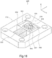
- Fig. 16 shows an example of the structure of a scanner 300 conventionally used.
- the scanner 300 has a structure in which an inner frame 304 is supported on the inner side of an outer frame 310 via plate springs 302 that can be deflected in the Y direction, and a base portion 307 is supported on the inner side of the inner frame 304 via plate springs 305 that can be deflected in the X direction.
- a Y actuator 303 that expands and contracts in the Y direction in accordance with an applied voltage, and the members supported by the inner frame 304 and the inner frame 304 move relative to the outer frame 310 in the Y direction in accordance with the expansion and contraction of the Y actuator 303.
- An X actuator 306 that expands and contracts in the X direction in accordance with an applied voltage is provided between the inner side surface of the inner frame 304 and the outer side surface of the base portion 307, and members supported by the base portion 307 and the base portion 307 move relatively in the X direction with respect to the inner frame 304 and the outer frame 310 in accordance with expansion and contraction of the X actuator 306.
- a stage 309 is provided on the base portion 307 via a Z actuator 308 that expands and contracts in the Z direction in accordance with an applied voltage. In accordance with the expansion and contraction of the Z actuator 308, the stage 309 and the sample disposed on the stage 309 move relatively in the Z direction with respect to the base portion 307 and the outer frame 310.
- the Y actuator 303 and the X actuator 306 are driven by the control signal to displace the stage 309 in the X-Y direction
- the Z actuator 308 is driven by the control signal to displace the stage 309 in the Z direction.
- the XYZ scanner 300 having the above-described structure is used in a high-speed scanning probe microscope (for example, see Non-Patent Document 1) because the number of resonance peaks can be reduced by a relatively simple structure and the resonance frequency can be relatively increased by increasing the strength (rigidity) of the scanner.
- the objects to be measured by the scanning probe microscope are various, and besides the surfaces of materials such as metals, semiconductors, ceramics and the like which have been measured from the past, cells, protein molecules and the like are also objects to be measured in recent years in the field of medical and biological research.
- Conventional measurements of protein molecules were obtained by imaging the protein molecules which are taken out of the cells and fixed on a support substrate, but not by imaging molecules actually functioning in the cells. Assuming imaging of molecules that are actually functioning in a cell, it is necessary to be compatible with imaging of a micrometer scale entire cell and imaging of nanometer scale protein molecules in the region in which the protein molecules are present in the cell.
- Non-patent Document 1 T. Ando et al. , e-J. Surf. Sci. Nanotech. 3, 384 (2005 )
- a scanner comprises an outer frame; a first inner frame disposed inside the outer frame; a wide range Y actuator for moving the first inner frame relative to the outer frame in the Y direction; a second inner frame disposed inside the first inner frame; a wide range X actuator for moving the second inner frame relative to the first inner frame in the X direction orthogonal to the Y direction; a third inner frame disposed inside the second inner frame; a narrow range Y actuator for moving the third inner frame relative to the second inner frame in the Y direction; a movable base disposed inside the third inner frame; and a narrow range X actuator for moving the movable base relative to the third inner frame in the X direction.
- the scanner may further comprise a stage supported by the movable base.
- the range in which the stage can be moved by the wide range X actuator may be wider than the range in which the stage can be moved by the narrow range X actuator
- the range in which the stage can be moved by the wide range Y actuator may be wider than the range in which the stage can be moved by the narrow range Y actuator.
- the stage may be supported on a movable base via a Z actuator that moves the stage relatively in a Z direction orthogonal to the X direction and the Y direction.
- a counter balance having a weight substantially equal to the total weight of the Z actuator and the stage may be attached to the surface of the movable base opposite to the surface on which the stage is supported via the Z actuator.
- the first inner frame may be connected to the outer frame via a plurality of plate springs whose plate surfaces are substantially orthogonal to the Y direction
- the second inner frame may be connected to the first inner frame via a plurality of plate springs whose plate surfaces are substantially orthogonal to the X direction
- the third inner frame may be connected to the second inner frame via a plurality of plate springs whose plate surfaces are substantially orthogonal to the Y direction
- the movable base may be connected to the third inner frame via a plurality of plate springs whose plate surfaces are substantially orthogonal to the X direction.
- a movable base counterpart having a weight substantially equal to that of the movable base is further provided inside the third inner frame, and the narrow range X actuator is a piezoelectric element which can expand and contract in the X direction in response to a control signal, and is preferably disposed between the movable base and the movable base counterpart.
- the wide range Y actuator may be a piezoelectric element which can expand and contract in the Y direction in response to the control signal, and may be disposed between the inner side surface of the outer frame and outer side surface of the first inner frame.
- the wide range X actuator may be a piezoelectric element which can expand and contract in the X direction in response to the control signal, and may be disposed between the inner side surface of the outer frame or the inner side surface of the first inner frame and the outer side surface of the second inner frame.
- the narrow range Y actuator may be a piezoelectric element which can expand and contract in the Y direction in response to the control signal, and may be disposed between the inner side surface of the second inner frame and the outer side surface of the third inner frame.
- the probe may be supported by a movable base.
- the scanner can be applied to a scanning probe microscope of a type in which the probe side is displaced for scanning.
- the scanner may further comprise a wide range Z actuator for moving the outer frame relative to a support base in the Z direction.
- a wide range Z actuator for moving the outer frame relative to a support base in the Z direction.
- the movable range by the wide range Z actuator is wider than the movable range by the Z actuator described above.
- a scanner comprises a supported body; a movable base supporting the supported body; a narrow range Z actuator disposed between the movable base and the supported body for moving the supported body relative to the movable base in the Z direction; an XY scanner for supporting the movable base and relatively moving the movable base in the X and Y directions; and a wide range Z actuator disposed between the XY scanner and a support base for moving the XY scanner relative to the support base in the Z direction.
- the movable range by the wide range Z actuator may be wider than the movable range by the narrow range Z actuator.
- the scanner may further comprise a flat plate-like support plate, and the wide range Z actuator may be attached to the first side of the support plate.
- the scanner may further include a counter wide range actuator provided at a position facing the wide range Z actuator on the second surface, which is the surface opposed to the first surface, and having the same characteristics as the wide range Z actuator, and a counter balance supported by the counter wide range Z actuator and having a weight substantially equal to the total weight of the support, the movable base, the narrow range Z actuator, and the XY scanner.
- a scanning probe microscope according to the present invention is characterized by including any one of the above-mentioned scanners.
- FIG. 1 is a drawing schematically showing a configuration of a scanning probe microscope according to a first embodiment of the present invention, and shows a configuration example of an atomic force microscope 1 as a specific example of the scanning probe microscope.
- Atomic force microscope 1 is a microscope that uses a cantilever chip 110 as a probe (a member to which a probe 114, which is a very microscopic projection at the tip of cantilever 112, is applied) to image the undulation of the sample surface through a change in cantilever 112 due to the interaction between probe 114 and the sample surface (such as displacement of the tip of the cantilever by an atomic force in a DC mode (contact mode or non-contact mode) or a change in cantilever vibration in an AC mode (sometimes referred to as a tapping mode).
- a DC mode contact mode or non-contact mode
- AC mode sometimes referred to as a tapping mode
- the atomic force microscope 1 includes a microscope chassis 100, a cantilever chip 110, an optical sensor unit 116, a stage 122, a scanner 200, a controller 102, a computer 104, and a monitor 106.
- the cantilever chip 110 is a member in which an extremely minute probe 114 is provided on the tip end of the cantilever 112.
- the cantilever chip 110 is fixed to the microscope chassis 100 via an excitation piezoelectric body 115 for vibrating the cantilever 112 in order to perform measurement in the AC mode.
- the scanner 200 supports the stage 122, and moves the stage 122 in the X direction, the Y direction, and the Z direction relative to a probe mounted on the microscope chassis 100 serving as a support base.
- the scanner 200 is detachably attached to the microscope chassis 100.
- the stage 122 In a state in which the scanner 200 is attached to the microscope chassis 100, the stage 122 is disposed at a position facing the probe 114 at the tip end of the cantilever 112.
- a sample (or a sample table holding the sample) to be measured by the atomic force microscope 1 is fixed to the stage 122.
- Figs. 2-5 show the structure of scanner 200 along with stage 122.
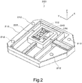
- Fig. 2 is a perspective view showing the configuration of a scanner stage unit 120.
- Fig. 3 is a plan view showing the configuration of the scanner stage unit 120.
- Fig. 4 is a partially enlarged view showing the configuration of the scanner 200.
- Fig. 5 is a cross-sectional view of the scanner 200 taken along the A-A' of Fig. 4 .
- the scanner 200 has a structure in which a narrow range XY scanner 230 whose scanning range is narrower than that of a wide range XY scanner 220 is supported in a nested state in the wide range XY scanner 220, and the wide range XY scanner 220 and the narrow range XY scanner 230 are accommodated in an outer frame 210.
- the stage 122 is supported by the narrow range XY scanner 230 via the Z actuator 240.
- the outer frame 210 is a frame body having high rigidity, and is formed of metal such as Invar, for example.
- the outer dimensions of the outer frame 210 are each about 50 mm in length and width (X direction and Y direction), for example, about 5 mm in thickness (Z direction) .
- the outer frame 210 is provided with a guide hole 212 for alignment with the microscope chassis 100. By screwing through the guide hole 212 and securing it to the microscope chassis 100, the scanner 200 can be attached to the correct position of the microscope chassis 100.
- the outer frame 210 has an opening for accommodating the scanner 200 inside while having a thickness sufficient to maintain strength. As shown in Fig. 3 , the outer frame 210 has inner side surfaces 214 and 215 parallel to the Y-Z plane and an inner side surface 216 parallel to the X-Z plane.
- the wide range XY scanner 220 includes a first inner frame 222, a wide range Y actuator 224, a second inner frame 226, and a wide range X actuator 228.
- the first inner frame 222 is a U-shaped frame body, and includes a side wall portion 222a, a connection portion 222b, and a side wall portion 222c.
- the side wall portion 222a and the side wall portion 222c are flat plate portions parallel to the X-Z plane.
- the connection portion 222b is a flat plate portion parallel to the Y-Z plane, and connects the side wall portion 222a and the side wall portion 222c.
- the first inner frame 222 is connected to the inner side surfaces 214 and 215 parallel to the Y-Z plane of the outer frame 210 at both ends of the side wall portion 222a and the side wall portion 222c in the Y direction via four plate springs 223 .
- the plate spring 223 is provided so that the plate surface is substantially parallel to the X-Z plane (in other words, the plate surface is substantially orthogonal to the Y direction), and when the plate spring 223 is bent, the first inner frame 222 can move in the Y direction with respect to the outer frame 210, but the movement in the X direction and the Z direction is restricted.
- the outer side surface of the side wall portion 222c of the first inner frame 222 is parallel to the X-Z plane.
- the outer side surface of the side wall portion 222c and the inner side surface 216 of the outer frame 210 parallel to the X-Z plane are disposed so as to face each other, and the wide range Y actuator 224 is disposed therebetween.
- the wide range Y actuator 224 is formed of a piezoelectric element such as a piezoelectric element, for example.
- the wide range Y actuator 224 has a free length, i.e., a length in a natural state in which a control signal is not applied, substantially equal to the gap between the outer side surface of the side wall portion 222c and the inner side surface 216 of the outer frame 210.
- the wide range Y actuator 224 expands and contracts in response to a control signal from the controller 102, and relatively moves the first inner frame 222 in the Y direction with respect to the outer frame 210 while deflecting the plate springs 223 in the Y direction.
- the wide range Y-actuator 224 may have an expansion coefficient that causes a displacement in the Y direction on a micrometer scale (e.g., 10 micrometers) when a maximum voltage (e.g., 100 volts) is applied.
- the second inner frame 226 is a rectangular frame body, and includes a side wall portion 226a, a side wall portion 226b, a side wall portion 226c, and a side wall portion 226d.
- the side wall portion 226a and the side wall portion 226c are flat plate portions parallel to the X-Z plane.
- the side wall portion 226b and the side wall portion 226d are flat plate portions parallel to the Y-Z plane, and connect the side wall portion 226a and the side wall portion 226c, respectively.
- the side wall portion 226a is connected to an inner side surface of the side wall portion 222a in the vicinity of the center in the X direction, the inner side surface being parallel to the X-Z plane, via a plate spring 227.
- the side wall portion 226c is connected to the inner side surface of the side wall portion 222c in the vicinity of the center in the X direction, which is parallel to the X-Z plane, via a plate spring 227.
- the plate springs 227 is provided so that the plate surface is parallel to the Y-Z plane (in other words, the plate surface is substantially orthogonal to the X direction), and the second inner frame 226 can move in the X direction with respect to the outer frame 210 and the first inner frame 222 by deflecting the plate spring 227, but the movement in the Y direction and the Z direction is restricted.
- the outer side surface of the side wall portion 226d is parallel to the Y-Z plane, and is disposed so as to face the inner side surface 215 of the outer frame 210 parallel to the Y-Z plane.
- the wide range X actuator 228 is disposed between the outer side surface of the side wall portion 226b and the inner side surface 214 of the outer frame 210.
- the wide range X actuator 228 is formed of a piezoelectric element such as a piezoelectric element, for example.
- the wide range X actuator 228 has a free length substantially equal to the gap between the outer side surface of the side wall portion 226b and the inner side surface 214 of the outer frame 210.
- the wide range X actuator 228 expands and contracts in response to a control signal from the controller 102, and moves the second inner frame 226 relative to the outer frame 210 and the first inner frame 222 in the X direction while deflecting the plate spring 227 in the X direction.
- the wide range X-actuator 228 may have an expansion coefficient that causes a displacement in the X direction on a micrometer scale (e.g., 10 micrometers) when a maximum voltage (e.g., 100 volts) is applied.
- the wide range XY scanner 220 realizes a wide range XY scan in accordance with the control signal on the inner side of the outer frame 210.
- the narrow range XY scanner 230 includes a third inner frame 232, a narrow range Y actuator 234, a movable base 236, a movable base counterpart 237, and a narrow range X actuator 238.
- the third inner frame 232 is a substantially rectangular frame body, and includes a side wall portion 232a, a connection portion 232b, a side wall portion232c, and a connection portion 232d.
- the side wall portion 232a and the side wall portion 232c are flat plate portions parallel to the X-Z plane.
- the connection portion 232b and the connection portion 232d are flat plate portions parallel to the Y-Z plane, and connect the side wall portion 232a and the side wall portion 232c, respectively.
- the connection portion 232b and the connection portion 232d are connected to the inner side surface of the side wall portion 226b and the side wall portion 226d of the second inner frame 226 parallel to the Y-Z plane via the plate springs 233 at both ends in the Y direction.
- the plate spring 233 is provided so that the plate surface is substantially parallel to the X-Z plane (in other words, the plate surface is substantially orthogonal to the Y direction), and the third inner frame 232 can be moved in the Y direction with respect to the wide range XY scanner 220 by deflecting the plate spring 233, but the movement in the X direction and the Z direction is restricted.
- the outer side surface of the side wall portion 232c is parallel to the X-Z plane.
- the outer side surface of the side wall portion 232c and the inner side surface of the side wall portion 226c parallel to the X-Z plane are disposed so as to face each other, and the narrow Y actuator 234 is disposed therebetween.
- the narrow Y actuator 234 is formed of a piezoelectric element such as a piezoelectric element, for example.
- the narrow Y actuator 234 has a free length, i.e., a length in a natural state in which a control signal is not applied, substantially equal to the gap between the outer side surface of the side wall portion 232c and the inner side surface of the side wall portion 226c.
- the narrow range Y actuator 234 expands and contracts in response to a control signal from the controller 102, and moves the third inner frame 232 relative to the wide range XY scanner 220 in the Y direction while deflecting the plate spring 233 in the Y direction.
- the narrow Y actuator 234 may have an expansion coefficient that produces a nanometer scale (e.g., 700 nanometers) displacement in the Y direction when a maximum voltage (e.g., 100 volts) is applied.
- the movable base 236 is a substantially rectangular parallelepiped block. Both ends of the movable base 236 in the X direction are connected to the inner side surfaces of the side wall portions 232a and 232c via plate springs 239. Here, the movable base 236 is connected to the vicinity of one end in the X direction of the side wall 232a and the side wall 232c.
- the plate spring 239 is provided so that the plate surface is parallel to the Y-Z plane (in other words, the plate surface is substantially orthogonal to the X direction), and the movable base 236 can move in the X direction with respect to the wide range XY scanner 220 by deflecting the plate spring 239, but the movement in the Y direction and the Z direction is restricted.
- the stage 122 is disposed on a first surface of the movable base 236 parallel to the X-Y plane via a Z actuator 240.
- the Z actuator 240 is formed of, for example, a piezoelectric element such as a piezoelectric element, and expands and contracts in the Z direction in response to an applied control signal.
- a control signal corresponding to the measurement mode is applied to the Z actuator 240 by the controller 102.
- a signal for controlling the change of the vibration of the cantilever to be constant is applied, and the position in the Z direction is changed following the change of the distance between the sample surface and the cantilever in accordance with the XY scan.
- a counter balance 242 having a weight substantially equal to the combined weight of the Z actuator 240 and the stage 122 is disposed on a second surface of the movable base 236 opposite to the first surface.
- the counter balance 242 balances the load weight driven by the narrow range X actuator 238 in the Z direction.
- the counter balance 242 includes a counter actuator 242a similar to the Z actuator 240 and a counter stage 242b similar to the stage 122.
- the same control signal as that applied to the Z actuator 240 is applied to the counter actuator 242a by the controller 102, and the counter actuator 242a expands and contracts in the same manner as the Z actuator 240 in response to the control signal.
- Such a structure and control can prevent the center of gravity of the load weight of the narrow range X actuator 238 from fluctuating in the Z direction as the Z actuator 240 expands and contracts. In this manner, the narrow X actuator 238 can achieve displacement in the X direction while maintaining balance in the Z direction. As a result, the resonance frequency of the structure including the movable base 236, the movable base counterpart 237, and the like arranged inside the third inner frame 232 is increased, which can contribute to realization of high-speed scanning.
- the counter balance 242 may have a weight substantially equal to the combined weight of the Z actuator 240 and the stage 122, but from the standpoint of suppressing the movement of the center of gravity due to expansion and contraction of the Z actuator 240, the configuration including the counter actuator 242a described above is more preferable.
- the movable base counterpart 237 is a substantially rectangular parallelepiped block. Both ends of the movable base counterpart 237 in the X direction are connected to the inner side surfaces of the side wall portions 232a and 232c via plate springs 239. Here, the movable base counterpart 237 is connected to the vicinity of the other end in the X direction of the side wall portion 232a and the side wall portion 232c, that is, the end on the side to which the movable base 236 is not connected.
- the plate spring 239 is provided so that the plate surface is parallel to the Y-Z plane, and the movable base 236 can move in the X direction with respect to the wide range XY scanner 220 by deflecting the plate spring 239, but the movement in the Y direction and the Z direction is restricted.
- the movable base counterpart 237 has a weight substantially equal to that of the movable base 236.
- a weight (not shown) having a weight substantially equal to the total weight of the Z actuator 240, the counter balance 242, and the stage 122 is mounted on the movable base counterpart 237.
- a narrow range X actuator 238 is disposed between the movable base 236 and the movable base counterpart 237.
- the narrow range X actuator 238 is formed of a piezoelectric element such as a piezoelectric element, for example.
- the narrow X actuator 238 has a free length substantially equal to the gap between the movable base 236 and the movable base counterpart 237.
- the narrow range X actuator 238 expands and contracts in response to a control signal from the controller 102, and pushes the movable base 236 and the movable base counterpart 237 in opposite directions in the X direction while deflecting the plate spring 239 in the X direction.
- the movable base 236 and the movable base counterpart 237 are of substantially equal weight and a weight of substantially equal weight to the total weight of the Z actuator 240, the counter balance 242, and the stage 122 supported by the movable base 236 is attached to the movable base counterpart 237, the narrow range X actuator 238 can be driven in the X direction in a balanced manner (with equal loads on both sides).
- the resonance frequency of the structure including the movable base 236, the movable base counterpart 237, and the like arranged inside the third inner frame 232 is increased, which can contribute to realization of high-speed scanning.
- the narrow-range X-actuator 238 may have an expansion coefficient that results in a nanometer-scale (e.g., 700 nanometers) displacement in the X-direction with respect to the movable base 236 when a maximum voltage (e.g., 100 volts) is applied.
- a nanometer-scale e.g. 700 nanometers
- a maximum voltage e.g. 100 volts
- the narrow range XY scanner 230 realizes a narrow range XY scan in accordance with the control signal inside the wide range XY scanner 220.
- the scanning range of the narrow range XY scanner 230 is narrower than that of the wide range XY scanner 228, the narrow range XY scanner 230 has a resonance frequency higher than that of the wide range XY scanner 220 and can perform high-speed scanning because of the light weight and the simple structure of the mass to be driven during scanning.
- the narrow range Y actuator 234 and the narrow range X actuator 238 of the narrow range XY scanner 230 have an expansion coefficient smaller than that of the wide range Y actuator 224 and the wide range X actuator 228 of the wide range XY scanner 220, scanning with high positional accuracy is possible although the scanning range is narrowed.
- the outer frame 210, the first inner frame 222, the plate springs 223, the second inner frame 226, the plate springs 227, the third inner frame 232, the plate springs 233, the movable base 236, the movable base counterpart 237, and the plate springs 239 are integrally formed of metal such as invar, for example.
- a buffer material such as a urethane resin may be filled in the space inside the outer frame 210 where the wide range XY scanner 220 and the narrow range XY scanner 230 are not disposed in order to absorb shock.
- the optical sensor unit 116 detects the displacement of the cantilever 112 based on the interaction between the probe 114 at the tip of the cantilever 112 and the sample surface, and outputs a signal based on the displacement.
- the optical sensor unit 116 may comprise, for example, a sensor known as an optical lever type optical sensor.
- the optical lever type optical sensor irradiates the back surface of the cantilever 112 with a laser beam through an optical system such as a lens, a mirror, or the like as necessary, and receives the reflected light by a photodiode.
- the optical lever type optical sensor detects the displacement of the cantilever 112 as the movement of the laser light spot on the photodiode.
- the scanner 200 is connected to the controller 102, and the optical sensor unit 116 for detecting the displacement of the cantilever 112 is connected to the computer 104.
- a monitor 106 is connected to the computer 104.
- the controller 102 includes, for example, a laser diode drive circuit, a preamplifier circuit, an oscillator circuit, a AC/DC converter circuit, a feedback circuit, a scan control circuit, an actuator drive circuit, and the like.
- the controller 102, the computer 104, and the monitor 106 perform control and driving of the atomic force microscope mechanism and signal processing, and finally display the unevenness information of the sample on the monitor 106, whereby the user can obtain knowledge on the surface information of the sample.
- a wide range scan is performed using the wide range XY scanner 220, and observation of a sample surface on a micrometer scale is performed.
- This wide range scan is relatively slow, e.g., on the order of 0.5 seconds per frame, but a wide range of samples can be captured in one image.
- a point of interest to be a target of the narrow range scanning is specified.
- a voltage is applied to the wide range Y actuator 224 and the wide range X actuator 228 of the wide range XY scanner 220 so that the point of interest becomes the reference position of the narrow range scanning. That is, the wide range XY scanner 220 realizes the offset to the position where the narrow range scanning is performed. In this state, narrow range scanning is performed by the narrow range XY scanner 230.
- the narrow scan is relatively fast, e.g., 30 milliseconds per frame, and can visualize the dynamics of the point of interest.
- Fig. 1 an observation in a liquid is depicted, and a water droplet W is suspended from the vicinity of the sample of the scanner stage unit 120 to the vicinity of the cantilever chip 110, and both the sample and the cantilever chip 110 are located in the water.
- the atomic force microscope 1 is capable of observation in a liquid, which is an indispensable requirement when observing a living biological sample. When the measurement is performed in the air, this water is unnecessary.
- the scanning probe microscope according to the second embodiment of the present invention enables both wide range measurement in the Z direction and high-speed and high-precision measurement.
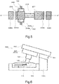
- Fig. 6 is a diagram schematically and roughly showing a configuration of a scanning probe microscope (an atomic force microscope 1) according to the second embodiment of the present invention.
- the cantilever 112 is supported by the microscope chassis 100.
- the microscope chassis 100 has a support post 100a, and a scanner is attached to the support post 100a.
- the scanner 500 of the present embodiment includes a wide range Z actuator 501, a support plate 502, an XY scanner 503, a movable base 503a, and a narrow range Z actuator 504.
- the scanner 500 is connected to a controller and driven similarly to the scanner 200 in the first embodiment.
- the support plate 502 is a flat and high-rigidity plate material, and supports the XY scanner 503 as shown in Fig. 6 .
- the XY scanner 503 moves the movable base 503a in the X direction and the Y direction.
- the XY scanner 503 may have a configuration in which the wide range XY scanner and the narrow range XY scanner are nested similarly to the scanner 200 in the first embodiment, or may be a single XY scanner.
- the movable base 503a supports the stage 122 via the narrow range Z actuator 504.
- the narrow range Z actuator 504 is disposed between the movable base 503a and the stage 122, and moves the stage 122 in the Z direction in a scanning range narrower than that of the wide range Z actuator 501.
- the wide range Z actuator 501 is formed of, for example, a piezoelectric element such as a piezoelectric element.
- the wide range Z actuator 501 is disposed between the XY scanner and the microscope chassis 100 which is a support base, and moves the XY scanner 503 relative to the support base in the Z direction.
- the wide range Z actuator 501 supports, directly or indirectly, the XY scanner 503, the movable base 503a, the narrow range Z actuator 504, and the stage 122. With such a configuration, the wide range Z actuator 501 moves the stage 122 in the Z direction in a wider range than the narrow range Z actuator 504.
- the narrow range Z actuator 504 moves the stage in the Z direction while being supported by the wide range Z actuator 501.
- the scanning range of the narrow-range Z actuator 504 is narrower than the scanning range by the wide-range Z actuator 501, the resonant frequency is higher than that of the wide-range Z actuator 501 because the weight to be driven is only the stage and it is lightweight, and therefore high-speed scanning is possible.
- the narrow range Z actuator 504 has an expansion coefficient smaller than that of the wide range Z actuator 501, the resolution in the Z direction can be enhanced.
- the narrow range Z actuator 504 in a state where the narrow range Z actuator 504 is fixed to a reference position, for example, a center position of the narrow range scan, the rough shape of the sample is observed at a substantially micrometer scale in a scanning range in a large Z direction by using the wide range Z actuator 501.
- the frequency characteristic or the like of the wide range Z actuator 501 restricts the band of the feedback control, and the speed becomes low (e.g., about 10 seconds/frame), but a sample having a large structure over a wide Z-direction range (e.g., cells) can be captured in one image.
- a point of interest to be a target of the narrow range scanning is specified.
- the point of interest is a region (for example, a surface molecule of a cell membrane) in which the change in the Z direction (that is, the unevenness of the sample) is relatively small.
- a voltage is applied to the wide range Z actuator 501 so that the point of interest becomes the reference position of the narrow range scanning. That is, the wide range Z actuator 501 realizes the offset to the position in the Z direction where the narrow range scanning is performed.
- the scanning range is narrowed as compared with that in the wide range scanning while offsetting to a point of interest to be a target of the narrow range scanning.
- a narrow range scanning is performed using the XY scanner 503 and the narrow range Z actuator 504.
- the narrow range scanning is relatively fast, e.g., 30 milliseconds per frame, and the point of interest can be observed on a nanometer scale.
- the dynamic state of the target portion can be visualized.
- Example 1 In raster scanning in which scanning lines are sequentially moved in the Y direction while scanning is performed one-dimensionally in the X direction, scanning in the X direction becomes the highest speed, which is the rate-limiting of the entire scanning speed. That is, scanning in the X direction is a main factor that limits the frame rate and the temporal resolution of an image. It is the frequency below which the resonance peak appears in the frequency characteristic that the scanner can be accurately displaced according to the control signal. Therefore, in Example 1 described below, the scanner 200 having the structure shown in Figs. 2 to 5 was manufactured and applied to an atomic force microscope, and the frequency characteristics (gain vs. frequency) of the X-direction scanning of the wide range XY scanner 220 and the narrow range XY scanner 230 were compared with the frequency characteristics of the X-direction scanning in the conventional scanner (Comparative Example 1).
- a scanner 200 having the structure shown in Fig. 2 was used.
- the expansion coefficient of the wide range X actuator 228 was 40 nm/V (i.e., 4 ⁇ m for the maximum scan range applied from 0 to 100 volts), and the expansion coefficient of the narrow range X actuator 238 was 7 nm/V (i.e., 700 nm for the maximum scan range applied from 0 to 100 volts) .
- the maximum scanning range of the wide range Y actuator 224 was 8 ⁇ m
- the maximum scanning range of the narrow range Y actuator 234 was 1.5 ⁇ m.
- Fig. 7 shows the frequency characteristic of the X scanning by the wide range XY scanner 220.
- the horizontal axis represents the frequency (drive frequency) of the triangular wave for driving the X scanner
- the vertical axis represents the displacement (gain) at each drive frequency.
- the frequency characteristic of the X-scan by the wide range XY scanner 220 has the first resonance peak at about 3.5 kHz. With the first resonance peak at this frequency, an image of 100 pixels each in the vertical and horizontal directions for the maximum scanning range (4 ⁇ m in the X direction and 8 ⁇ m in the Y direction) by the wide range XY scanner 220 can be acquired at 0.6 sec/frame. It is possible to scan the same scanning range at the same speed as compared with the scanner 400 of the conventional type which will be described later as a comparative example.
- Fig. 8 shows the frequency characteristic of the X scanning by the narrow range XY scanner 230.
- the frequency characteristic of the X scanning by the narrow-range XY scanner 230 has the first resonance peak at about 60 kHz. With the first resonance peak at this frequency, an image of 100 pixels each in the vertical and horizontal directions for the maximum scanning range (700 nm in the X direction, 1.5 ⁇ m in the Y direction) by the narrow-range XY scanner 230 can be acquired at 33 milliseconds per frame. This means that the frame rate is about 30 fps, and the measurement result of the atomic force microscope 1 or the like can be obtained as a relatively smooth moving image.
- the structure of the scanner 400 used as Comparative Example 1 is shown in Fig. 9 .
- the scanner 400 has a structure in which an inner frame 404 is supported on the inner side of an outer frame 410 via a plate springs 402 that can be deflected in the Y direction, and a base portion 407 is supported on the inner side of the inner frame 404 via a plate springs 405 that can be deflected in the X direction.
- a Y actuator 403 that expands and contracts in the Y direction in accordance with an applied voltage is provided.
- An X actuator 406 that expands and contracts in the X direction in accordance with an applied voltage is provided between the inner side surface of the outer frame 410 and the outer side surface of the base portion 407.
- a stage 409 is provided on the base portion 407 via a Z actuator 408 that expands and contracts in the Z direction in accordance with an applied voltage.
- the expansion coefficient of the X actuator 406 was 70 nm/V, that is, 7 ⁇ m in the maximum scanning range applied with 0 to 100 volts.
- the maximum scanning range in the Y direction was 6 ⁇ m.
- Fig. 10 shows the frequency characteristic of the X scan by the X actuator 406.
- the frequency characteristic of the X-scan by the conventional scanner 400 has the first resonance peak at about 7 kHz. With the first resonance peak at this frequency, an image of 100 pixels each in the vertical and horizontal directions for the maximum scanning range (7 ⁇ m in the X direction and 6 ⁇ m in the Y direction) by the scanner 400 can be acquired at 0.3 sec/frame
- the wide range XY scanner 220 can realize the wide range scanning at the same speed as that of the conventional type scanner.
- the narrow-range XY scanner 230 high-speed scanning can be realized to the extent that a smooth moving image can be acquired in the scanning range of the nanometer scale.
- the scanner 200 can perform both wide-range measurement and high-speed and high-precision measurement. As an application example, for example, when the scanner 200 is applied to a measurement system in a liquid as shown in Fig. 1 , appearance imaging of cells and dynamic imaging of protein molecules in living cells can be performed seamlessly.
- Example 2 the scanner 500 having the structure shown in Fig. 6 was manufactured and applied to an atomic force microscope, and the frequency characteristics (gain vs. frequency) of the Z-direction scanning of the wide range Z actuator 501 and the narrow range Z actuator 504 were compared with the frequency characteristics of the Z direction scanning in the conventional scanner (Comparative Example 2) .
- Example 2 a scanner 500 having the structure shown in Fig. 6 was used.
- the expansion coefficient of the wide range Z actuator was 25 nm/V (i.e., 2.5 ⁇ m for the maximum scanning range applied from 0 to 100 volts), and the expansion coefficient of the narrow range Z actuator 504 was 10 nm/V (i.e., 500 nm for the maximum scanning range applied from 0 to 50 volts) .
- Fig. 11 (a) shows the frequency characteristic of the Z scanning by the wide range Z actuator 501.
- the horizontal axis represents the frequency (drive frequency) of the triangular wave for driving the wide range Z actuator 501
- the vertical axis represents the displacement (gain) at each drive frequency.
- the frequency characteristic of the Z scanning by the wide range Z actuator 501 has the first resonance peak at about 1 kHz. Although this resonance peak may limit the bandwidth of the feedback control, images of 100 pixels each in the vertical and horizontal directions can be acquired at about 10 seconds/frame, which is about the same as when observing a sample having a large structure in a conventional wide range scan.
- Fig. 11 (b) shows the frequency characteristic of the Z scanning performed by the narrow range Z actuator 504.
- the frequency characteristic of the Z scanning by the narrow range Z actuator 504 has the first resonance peak at about 150 kHz. In the case of having the first resonance peak at this frequency, this resonance peak is not the rate limiting of the bandwidth of the feedback control, and images can be acquired at, for example, about 33 milliseconds/frame. This means that the frame rate is about 30 fps, and the measurement result of the atomic force microscope 1 or the like can be obtained as a relatively smooth moving image.
- the narrow range Z actuator 504 has an expansion coefficient smaller than that of the wide range Z actuator 501, the resolution in the Z direction can be improved.
- a conventional scanner 600 as shown in Fig. 12 was used.
- Scanner 600 does not have a wide range Z actuator and includes a single Z actuator 604 with a relatively large expansion coefficient.
- the Z actuator 604 is supported by the XY scanner 603.
- the expansion coefficient of the Z actuator 604 in the scanner 600 was 21 nm/V, i.e., 1.05 ⁇ m for the maximum scanning range applied from 0 to 50 volts.
- Fig. 13 shows the frequency characteristics of the Z scanning performed by the Z actuator 604 of Comparative Example 2.
- the frequency characteristic of the Z-scan by the conventional scanner 604 has the first resonance peak at about 80 kHz.
- this resonance peak is not the rate limiting of the bandwidth of the feedback control, and an image can be acquired at a relatively high speed.
- the expansion coefficient of the Z actuator is relatively large, the resolution in the Z direction is inferior to that of the narrow range Z actuator 504 in the second embodiment.
- scanning with a large area Z actuator can measure a sample with a large structure at a speed comparable to using a conventional actuator.
- high-speed and high-resolution scanning can be realized to the extent that a smooth moving image can be acquired in the scanning range of the nanometer scale.
- the scanner including the wide range Z actuator and the narrow range Z actuator the wide range measurement can be made compatible with the high-speed and high-precision measurements
- the scanner is applied to an atomic force microscope, it can also be applied to a probe microscope other than an atomic force microscope, and it can also be applied to a microscope other than a probe microscope as long as the measurement principle is not affected.
- the stage 122 is movable in the X direction, the Y direction, and the Z direction by the scanner 200. However, in the Z direction, not the stage but the probe may move.
- the stage 122 is movable in the X direction, the Y direction, and the Z direction by the scanner 200, but the probe may be moved by the scanner 200.
- the first inner frame 222 is a U-shaped frame body, and the wide range Y actuator 224 is configured to contact the inner side surface of the outer frame 210 through the missing portion of the first inner frame 222; however, the first inner frame 222 may be configured to be a rectangular frame body, and the wide range Y actuator 224 may be configured to contact the inner side surface of the first inner frame 222 instead of the outer frame 210.
- the movable base counterpart 237 having the same weight as the movable base 236 is disposed inside the third inner frame 232, and the narrow range X actuator 238 is disposed between the movable base 236 and the movable base counterpart 237; however, the narrow range X actuator 238 may be disposed between the second inner frame 226 and the third inner frame 232 without providing the movable base counterpart 237.
- a counter balance for maintaining the balance in the Z direction may be provided.
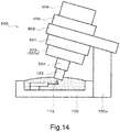
- the wide range Z actuator 501 may be fixed to one surface of the support plate 502, and the XY scanner 503 may be directly supported.
- a counter wide range Z actuator 505 having the same characteristics as the wide range Z actuator 501 may be provided on the other surface of the support plate 502.
- the counter wide range Z actuator 501 may support the XY scanner 503, the movable base 503a, the narrow range Z actuator 504, and a counter balance 506 equal in weight to the total weight of the stage 122 (and the sample) on the opposite side of the support plate 502.
- the support plate 502 is attached to the support post 100a of the microscope chassis 100. In this manner, the balance in the Z direction in the case where the wide range Z actuator 501 is used is maintained, and the band reduction of the XY scanner 503 due to the imbalance can be suppressed.
- the high-speed, high-resolution narrow range scanning and the wide-range coarse motion scanning can be made compatible with each other.
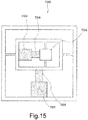
- a mechanical series configuration it is necessary to drive the wide and narrow actuators for one of the X or Y direction scans (in the configuration of Fig. 15 , the Y direction scans) with the stage 705 for the other scan.
- the driving bands of the narrow scanning and the wide scanning are necessarily lowered in one scanning direction, and high-speed scanning cannot be realized. For this reason, it is difficult to realize high-speed imaging of atomic and molecular levels in a scanner having a mechanical series configuration.
- the scanner according to the present invention employing the nested structure using the inner frame and the outer frame can speed up the fine movement scanning in both the X direction and the Y direction, thereby realizing the high-speed and high-resolution narrow-range scanning. Further, if the configuration of the narrow range scanning is miniaturized, the speed of the wide range scanning can be increased. In addition, scanning in the X direction and the Y direction is hardly interfered owing to the nested structure using the inner frame and the outer frame. For this reason, according to the scanner of the present invention, it is possible to perform high-speed imaging at the atomic and molecular levels, and it is possible to capture the kinetics of the atoms and molecules.
Landscapes
- Physics & Mathematics (AREA)
- Health & Medical Sciences (AREA)
- General Health & Medical Sciences (AREA)
- General Physics & Mathematics (AREA)
- Nuclear Medicine, Radiotherapy & Molecular Imaging (AREA)
- Radiology & Medical Imaging (AREA)
- Length Measuring Devices With Unspecified Measuring Means (AREA)
- Mechanical Optical Scanning Systems (AREA)
Abstract
Description
- The present invention relates to a scanning probe microscope for displacing a sample stage relative to a probe for scanning, and more particularly, to a structure of a scanner for performing the scanning.
- A scanning probe microscope (SPM) is a scanning microscope for mechanically scanning a mechanical probe to obtain information on sample surfaces, and is a generic name for a scanning tunneling microscope (STM), an atomic force microscope (AFM), a scanning magnetic force microscope (MFM), a scanning capacitance microscope (SCaM), a scanning near-field light microscope (SNOM), a scanning thermal microscope (SThM), and the like. In principle, a scanning probe microscope has, as a principle common element, a sample stage, a probe, a scanner for displacing the sample stage or the probe for scanning, and a detector for detecting a change in a physical quantity occurring in the probe. In the scanning probe microscope, the probe and the sample are raster-scanned relatively in the X and Y directions to obtain surface information of a desired sample region through the probe, and the surface information can be mapped and displayed on a monitor. In this specification, the height direction of the sample is defined as the Z direction, and two orthogonal directions in a plane orthogonal to the Z direction are defined as the X direction and the Y direction.
- A typical scanning probe microscope is an atomic force microscope. In an atomic force microscope, a cantilever chip (a member to which a very small probe is attached to the tip end of a cantilever) is used as a probe.
-
Fig. 1 is a diagram showing a configuration example of a main part of an atomic force microscope of a type in which a sample stage side is displaced for scanning. As shown inFig. 1 , in the sample stage displacement type apparatus, ascanner 200 for scanning astage 122 on which a sample is arranged is provided on amicroscope chassis 100. Thescanner 200 includes a Z scanner that can be displaced in the Z direction (the vertical direction in the figure) in response to a control signal from acontroller 102, and an X-Y scanner that can be displaced in the X-Y direction (two orthogonal directions along a plane perpendicular to the paper plane in the figure) . Thecantilever chip 110 has acantilever 112 and aprobe 114, and a base portion thereof is fixed to themicroscope chassis 100 via an excitationpiezoelectric body 115 or the like. - When the scanner is controlled by the
controller 102 and the sample is displaced, a change occurs in thecantilever 112, the change is detected by anoptical sensor unit 116, and from the data of each measurement point, the state of undulation of the sample surface is imaged by acomputer 104 and displayed on amonitor 106. The structure of each part of the atomic force microscope and the feedback control are described in detail in, for example,Patent Documents 1 and 2. -
Fig. 16 shows an example of the structure of ascanner 300 conventionally used. Thescanner 300 has a structure in which aninner frame 304 is supported on the inner side of anouter frame 310 viaplate springs 302 that can be deflected in the Y direction, and abase portion 307 is supported on the inner side of theinner frame 304 viaplate springs 305 that can be deflected in the X direction. Between the inner side surface of theouter frame 310 and the outer side surface of theinner frame 304, there is provided aY actuator 303 that expands and contracts in the Y direction in accordance with an applied voltage, and the members supported by theinner frame 304 and theinner frame 304 move relative to theouter frame 310 in the Y direction in accordance with the expansion and contraction of theY actuator 303. AnX actuator 306 that expands and contracts in the X direction in accordance with an applied voltage is provided between the inner side surface of theinner frame 304 and the outer side surface of thebase portion 307, and members supported by thebase portion 307 and thebase portion 307 move relatively in the X direction with respect to theinner frame 304 and theouter frame 310 in accordance with expansion and contraction of theX actuator 306. Astage 309 is provided on thebase portion 307 via aZ actuator 308 that expands and contracts in the Z direction in accordance with an applied voltage. In accordance with the expansion and contraction of theZ actuator 308, thestage 309 and the sample disposed on thestage 309 move relatively in the Z direction with respect to thebase portion 307 and theouter frame 310. In thescanner 300 having such a structure, theY actuator 303 and theX actuator 306 are driven by the control signal to displace thestage 309 in the X-Y direction, and theZ actuator 308 is driven by the control signal to displace thestage 309 in the Z direction. - In order to increase the time resolution of the scanning probe microscope (in other words, to shorten the time required to scan one frame), it is important to increase the resonance frequency (natural frequency) of the scanner itself, which is the rate-limiting factor of the response of the scanner. In this respect, the XYZ
scanner 300 having the above-described structure is used in a high-speed scanning probe microscope (for example, see Non-Patent Document 1) because the number of resonance peaks can be reduced by a relatively simple structure and the resonance frequency can be relatively increased by increasing the strength (rigidity) of the scanner. - The objects to be measured by the scanning probe microscope are various, and besides the surfaces of materials such as metals, semiconductors, ceramics and the like which have been measured from the past, cells, protein molecules and the like are also objects to be measured in recent years in the field of medical and biological research. Conventional measurements of protein molecules were obtained by imaging the protein molecules which are taken out of the cells and fixed on a support substrate, but not by imaging molecules actually functioning in the cells. Assuming imaging of molecules that are actually functioning in a cell, it is necessary to be compatible with imaging of a micrometer scale entire cell and imaging of nanometer scale protein molecules in the region in which the protein molecules are present in the cell.
- In the
conventional scanner 300 described above, high-speed scanning is realized in a scanning range on a nanometer scale, but when the scanning range is to be expanded, it is necessary to make theY actuator 303 and theX actuator 306 have a larger expansion coefficient (also referred to as an expansion/contraction amount per unit voltage, or a piezoelectric constant). However, when the expansion coefficients of theY actuator 303 and theX actuator 306 are increased, there is a problem that the response speed and the positional accuracy are lowered, and it is difficult to achieve both the measurement in a wide range and the measurement at high speed and high accuracy. - The problem of compatibility between wide-range measurement and high-speed and high-precision measurement as described above is a problem commonly existing not only in an atomic force microscope but also in a scanning probe microscope of a type in which a stage is displaced by a scanner.
-
- Patent Document 1:
WO 2010/087114 - Patent Document 2:
WO 2006/129561 A1 - [Non-patent Document 1] T. Ando et al. , e-J. Surf. Sci. Nanotech. 3, 384 (2005)
- It is an object of the present invention to solve the above-mentioned problems and provide a scanner capable of achieving both a wide range of measurements and a high-speed and high-precision measurement, and a scanning probe microscope equipped with such a scanner.
- In order to solve the above problems, a scanner according to an embodiment of the present invention comprises an outer frame; a first inner frame disposed inside the outer frame; a wide range Y actuator for moving the first inner frame relative to the outer frame in the Y direction; a second inner frame disposed inside the first inner frame; a wide range X actuator for moving the second inner frame relative to the first inner frame in the X direction orthogonal to the Y direction; a third inner frame disposed inside the second inner frame; a narrow range Y actuator for moving the third inner frame relative to the second inner frame in the Y direction; a movable base disposed inside the third inner frame; and a narrow range X actuator for moving the movable base relative to the third inner frame in the X direction. By doing so, it is possible to achieve both wide-range measurement and high-speed and high-precision measurement.
- In the present invention, the scanner may further comprise a stage supported by the movable base.
- In the present invention, the range in which the stage can be moved by the wide range X actuator may be wider than the range in which the stage can be moved by the narrow range X actuator, and the range in which the stage can be moved by the wide range Y actuator may be wider than the range in which the stage can be moved by the narrow range Y actuator.
- In the present invention, the stage may be supported on a movable base via a Z actuator that moves the stage relatively in a Z direction orthogonal to the X direction and the Y direction. In addition, a counter balance having a weight substantially equal to the total weight of the Z actuator and the stage may be attached to the surface of the movable base opposite to the surface on which the stage is supported via the Z actuator.
- In the present invention, the first inner frame may be connected to the outer frame via a plurality of plate springs whose plate surfaces are substantially orthogonal to the Y direction, the second inner frame may be connected to the first inner frame via a plurality of plate springs whose plate surfaces are substantially orthogonal to the X direction, the third inner frame may be connected to the second inner frame via a plurality of plate springs whose plate surfaces are substantially orthogonal to the Y direction, and the movable base may be connected to the third inner frame via a plurality of plate springs whose plate surfaces are substantially orthogonal to the X direction.
- In the present invention, a movable base counterpart having a weight substantially equal to that of the movable base is further provided inside the third inner frame, and the narrow range X actuator is a piezoelectric element which can expand and contract in the X direction in response to a control signal, and is preferably disposed between the movable base and the movable base counterpart.
- In the present invention, the wide range Y actuator may be a piezoelectric element which can expand and contract in the Y direction in response to the control signal, and may be disposed between the inner side surface of the outer frame and outer side surface of the first inner frame. The wide range X actuator may be a piezoelectric element which can expand and contract in the X direction in response to the control signal, and may be disposed between the inner side surface of the outer frame or the inner side surface of the first inner frame and the outer side surface of the second inner frame. The narrow range Y actuator may be a piezoelectric element which can expand and contract in the Y direction in response to the control signal, and may be disposed between the inner side surface of the second inner frame and the outer side surface of the third inner frame.
- In the present invention, the probe may be supported by a movable base. In this manner, the scanner can be applied to a scanning probe microscope of a type in which the probe side is displaced for scanning.
- In the present invention, the scanner may further comprise a wide range Z actuator for moving the outer frame relative to a support base in the Z direction. Here, it is preferable that the movable range by the wide range Z actuator is wider than the movable range by the Z actuator described above.
- A scanner according to another embodiment of the present invention comprises a supported body; a movable base supporting the supported body; a narrow range Z actuator disposed between the movable base and the supported body for moving the supported body relative to the movable base in the Z direction; an XY scanner for supporting the movable base and relatively moving the movable base in the X and Y directions; and a wide range Z actuator disposed between the XY scanner and a support base for moving the XY scanner relative to the support base in the Z direction.
- In the present invention, the movable range by the wide range Z actuator may be wider than the movable range by the narrow range Z actuator.
- The scanner may further comprise a flat plate-like support plate, and the wide range Z actuator may be attached to the first side of the support plate. The scanner may further include a counter wide range actuator provided at a position facing the wide range Z actuator on the second surface, which is the surface opposed to the first surface, and having the same characteristics as the wide range Z actuator, and a counter balance supported by the counter wide range Z actuator and having a weight substantially equal to the total weight of the support, the movable base, the narrow range Z actuator, and the XY scanner.
- In order to solve the above-mentioned problems, a scanning probe microscope according to the present invention is characterized by including any one of the above-mentioned scanners.
-
-
Fig. 1 is a diagram schematically showing the configuration of an atomic force microscope according to the first embodiment. -
Fig. 2 is a perspective view showing the configuration of the scanner according to the first embodiment. -
Fig. 3 is a plan view showing the configuration of the scanner according to the first embodiment. -
Fig. 4 is a partially enlarged view showing the configuration of the scanner according to the first embodiment. -
Fig. 5 is a cross-sectional view of the scanners according to the first embodiment taken along the A-A' inFig. 4 . -
Fig. 6 is a diagram schematically showing the configuration of an atomic force microscope according to the second embodiment. -
Fig. 7 is a graph showing the frequency characteristic of X scanning by the wide range XY scanner. -
Fig. 8 is a diagram showing the frequency characteristic of X scanning by a narrow range XY scanner. -
Fig. 9 is a diagram showing the structure of a scanner used as a comparative example. -
Fig. 10 is a diagram showing the frequency characteristic of X scanning by a conventional scanner. -
Fig. 11 (a) is a diagram showing the frequency characteristics of Z scanning by the wide range Z actuator.Fig. 11 (b) is a diagram showing the frequency characteristic of the Z scanning by the narrow range Z actuator. -
Fig. 12 is a schematic diagram showing a configuration of a probe microscope using a scanner provided with a conventional Z actuator. -
Fig. 13 is a diagram showing the frequency characteristics of Z scanning by a conventional Z actuator. -
Fig. 14 is a schematic diagram showing a configuration of a probe microscope using a scanner according to a modification of the second embodiment. -
Fig. 15 is a plan view showing an example of a scanner having a mechanical series configuration. -
Fig. 16 is a diagram showing an example of the structure of a scanner conventionally used. - Hereinafter, the configuration of the scanning probe microscope according to the first embodiment of the present invention will be described with reference to the drawings . In this specification, in each drawing showing the configuration of the scanning probe microscope, the shape, dimensions, and the like of the constituent elements may be exaggerated or deformed in order to explain the main features thereof, and the shape drawn in the drawing is not necessarily a faithful drawing of the shape of an actual object.
Fig. 1 is a drawing schematically showing a configuration of a scanning probe microscope according to a first embodiment of the present invention, and shows a configuration example of anatomic force microscope 1 as a specific example of the scanning probe microscope. -
Atomic force microscope 1 is a microscope that uses acantilever chip 110 as a probe (a member to which aprobe 114, which is a very microscopic projection at the tip ofcantilever 112, is applied) to image the undulation of the sample surface through a change incantilever 112 due to the interaction betweenprobe 114 and the sample surface (such as displacement of the tip of the cantilever by an atomic force in a DC mode (contact mode or non-contact mode) or a change in cantilever vibration in an AC mode (sometimes referred to as a tapping mode). - As shown in
Fig. 1 , theatomic force microscope 1 includes amicroscope chassis 100, acantilever chip 110, anoptical sensor unit 116, astage 122, ascanner 200, acontroller 102, acomputer 104, and amonitor 106. - As described above, the
cantilever chip 110 is a member in which an extremelyminute probe 114 is provided on the tip end of thecantilever 112. Thecantilever chip 110 is fixed to themicroscope chassis 100 via anexcitation piezoelectric body 115 for vibrating thecantilever 112 in order to perform measurement in the AC mode. - The
scanner 200 supports thestage 122, and moves thestage 122 in the X direction, the Y direction, and the Z direction relative to a probe mounted on themicroscope chassis 100 serving as a support base. Thescanner 200 is detachably attached to themicroscope chassis 100. In a state in which thescanner 200 is attached to themicroscope chassis 100, thestage 122 is disposed at a position facing theprobe 114 at the tip end of thecantilever 112. A sample (or a sample table holding the sample) to be measured by theatomic force microscope 1 is fixed to thestage 122. -
Figs. 2-5 show the structure ofscanner 200 along withstage 122.Fig. 2 is a perspective view showing the configuration of ascanner stage unit 120.Fig. 3 is a plan view showing the configuration of thescanner stage unit 120.Fig. 4 is a partially enlarged view showing the configuration of thescanner 200.Fig. 5 is a cross-sectional view of thescanner 200 taken along the A-A' ofFig. 4 . - The
scanner 200 has a structure in which a narrowrange XY scanner 230 whose scanning range is narrower than that of a widerange XY scanner 220 is supported in a nested state in the widerange XY scanner 220, and the widerange XY scanner 220 and the narrowrange XY scanner 230 are accommodated in anouter frame 210. Thestage 122 is supported by the narrowrange XY scanner 230 via theZ actuator 240. - The
outer frame 210 is a frame body having high rigidity, and is formed of metal such as Invar, for example. The outer dimensions of theouter frame 210 are each about 50 mm in length and width (X direction and Y direction), for example, about 5 mm in thickness (Z direction) . Theouter frame 210 is provided with aguide hole 212 for alignment with themicroscope chassis 100. By screwing through theguide hole 212 and securing it to themicroscope chassis 100, thescanner 200 can be attached to the correct position of themicroscope chassis 100. Theouter frame 210 has an opening for accommodating thescanner 200 inside while having a thickness sufficient to maintain strength. As shown inFig. 3 , theouter frame 210 has inner side surfaces 214 and 215 parallel to the Y-Z plane and aninner side surface 216 parallel to the X-Z plane. - As shown in
Fig. 3 , the widerange XY scanner 220 includes a firstinner frame 222, a widerange Y actuator 224, a secondinner frame 226, and a widerange X actuator 228. - The first
inner frame 222 is a U-shaped frame body, and includes aside wall portion 222a, aconnection portion 222b, and aside wall portion 222c. Theside wall portion 222a and theside wall portion 222c are flat plate portions parallel to the X-Z plane. Theconnection portion 222b is a flat plate portion parallel to the Y-Z plane, and connects theside wall portion 222a and theside wall portion 222c. The firstinner frame 222 is connected to the inner side surfaces 214 and 215 parallel to the Y-Z plane of theouter frame 210 at both ends of theside wall portion 222a and theside wall portion 222c in the Y direction via four plate springs 223 . Theplate spring 223 is provided so that the plate surface is substantially parallel to the X-Z plane (in other words, the plate surface is substantially orthogonal to the Y direction), and when theplate spring 223 is bent, the firstinner frame 222 can move in the Y direction with respect to theouter frame 210, but the movement in the X direction and the Z direction is restricted. - The outer side surface of the
side wall portion 222c of the firstinner frame 222 is parallel to the X-Z plane. The outer side surface of theside wall portion 222c and theinner side surface 216 of theouter frame 210 parallel to the X-Z plane are disposed so as to face each other, and the widerange Y actuator 224 is disposed therebetween. The widerange Y actuator 224 is formed of a piezoelectric element such as a piezoelectric element, for example. The widerange Y actuator 224 has a free length, i.e., a length in a natural state in which a control signal is not applied, substantially equal to the gap between the outer side surface of theside wall portion 222c and theinner side surface 216 of theouter frame 210. The widerange Y actuator 224 expands and contracts in response to a control signal from thecontroller 102, and relatively moves the firstinner frame 222 in the Y direction with respect to theouter frame 210 while deflecting the plate springs 223 in the Y direction. The wide range Y-actuator 224 may have an expansion coefficient that causes a displacement in the Y direction on a micrometer scale (e.g., 10 micrometers) when a maximum voltage (e.g., 100 volts) is applied. - The second
inner frame 226 is a rectangular frame body, and includes aside wall portion 226a, aside wall portion 226b, aside wall portion 226c, and aside wall portion 226d. Theside wall portion 226a and theside wall portion 226c are flat plate portions parallel to the X-Z plane. Theside wall portion 226b and theside wall portion 226d are flat plate portions parallel to the Y-Z plane, and connect theside wall portion 226a and theside wall portion 226c, respectively. - The
side wall portion 226a is connected to an inner side surface of theside wall portion 222a in the vicinity of the center in the X direction, the inner side surface being parallel to the X-Z plane, via aplate spring 227. Similarly, theside wall portion 226c is connected to the inner side surface of theside wall portion 222c in the vicinity of the center in the X direction, which is parallel to the X-Z plane, via aplate spring 227. The plate springs 227 is provided so that the plate surface is parallel to the Y-Z plane (in other words, the plate surface is substantially orthogonal to the X direction), and the secondinner frame 226 can move in the X direction with respect to theouter frame 210 and the firstinner frame 222 by deflecting theplate spring 227, but the movement in the Y direction and the Z direction is restricted. - The outer side surface of the
side wall portion 226d is parallel to the Y-Z plane, and is disposed so as to face theinner side surface 215 of theouter frame 210 parallel to the Y-Z plane. The widerange X actuator 228 is disposed between the outer side surface of theside wall portion 226b and theinner side surface 214 of theouter frame 210. The widerange X actuator 228 is formed of a piezoelectric element such as a piezoelectric element, for example. The widerange X actuator 228 has a free length substantially equal to the gap between the outer side surface of theside wall portion 226b and theinner side surface 214 of theouter frame 210. The widerange X actuator 228 expands and contracts in response to a control signal from thecontroller 102, and moves the secondinner frame 226 relative to theouter frame 210 and the firstinner frame 222 in the X direction while deflecting theplate spring 227 in the X direction. The wide range X-actuator 228 may have an expansion coefficient that causes a displacement in the X direction on a micrometer scale (e.g., 10 micrometers) when a maximum voltage (e.g., 100 volts) is applied. - With such a configuration, the wide
range XY scanner 220 realizes a wide range XY scan in accordance with the control signal on the inner side of theouter frame 210. - As shown in
Fig. 4 , the narrowrange XY scanner 230 includes a thirdinner frame 232, a narrowrange Y actuator 234, amovable base 236, amovable base counterpart 237, and a narrowrange X actuator 238. - The third
inner frame 232 is a substantially rectangular frame body, and includes aside wall portion 232a, aconnection portion 232b, a side wall portion232c, and aconnection portion 232d. Theside wall portion 232a and theside wall portion 232c are flat plate portions parallel to the X-Z plane. Theconnection portion 232b and theconnection portion 232d are flat plate portions parallel to the Y-Z plane, and connect theside wall portion 232a and theside wall portion 232c, respectively. Theconnection portion 232b and theconnection portion 232d are connected to the inner side surface of theside wall portion 226b and theside wall portion 226d of the secondinner frame 226 parallel to the Y-Z plane via the plate springs 233 at both ends in the Y direction. Theplate spring 233 is provided so that the plate surface is substantially parallel to the X-Z plane (in other words, the plate surface is substantially orthogonal to the Y direction), and the thirdinner frame 232 can be moved in the Y direction with respect to the widerange XY scanner 220 by deflecting theplate spring 233, but the movement in the X direction and the Z direction is restricted. - The outer side surface of the
side wall portion 232c is parallel to the X-Z plane. The outer side surface of theside wall portion 232c and the inner side surface of theside wall portion 226c parallel to the X-Z plane are disposed so as to face each other, and thenarrow Y actuator 234 is disposed therebetween. Thenarrow Y actuator 234 is formed of a piezoelectric element such as a piezoelectric element, for example. Thenarrow Y actuator 234 has a free length, i.e., a length in a natural state in which a control signal is not applied, substantially equal to the gap between the outer side surface of theside wall portion 232c and the inner side surface of theside wall portion 226c. The narrowrange Y actuator 234 expands and contracts in response to a control signal from thecontroller 102, and moves the thirdinner frame 232 relative to the widerange XY scanner 220 in the Y direction while deflecting theplate spring 233 in the Y direction. Thenarrow Y actuator 234 may have an expansion coefficient that produces a nanometer scale (e.g., 700 nanometers) displacement in the Y direction when a maximum voltage (e.g., 100 volts) is applied. - The
movable base 236 is a substantially rectangular parallelepiped block. Both ends of themovable base 236 in the X direction are connected to the inner side surfaces of theside wall portions movable base 236 is connected to the vicinity of one end in the X direction of theside wall 232a and theside wall 232c. Theplate spring 239 is provided so that the plate surface is parallel to the Y-Z plane (in other words, the plate surface is substantially orthogonal to the X direction), and themovable base 236 can move in the X direction with respect to the widerange XY scanner 220 by deflecting theplate spring 239, but the movement in the Y direction and the Z direction is restricted. - The
stage 122 is disposed on a first surface of themovable base 236 parallel to the X-Y plane via aZ actuator 240. TheZ actuator 240 is formed of, for example, a piezoelectric element such as a piezoelectric element, and expands and contracts in the Z direction in response to an applied control signal. A control signal corresponding to the measurement mode is applied to theZ actuator 240 by thecontroller 102. For example, in the tapping mode, a signal for controlling the change of the vibration of the cantilever to be constant is applied, and the position in the Z direction is changed following the change of the distance between the sample surface and the cantilever in accordance with the XY scan. - As shown in
Fig. 5 , acounter balance 242 having a weight substantially equal to the combined weight of theZ actuator 240 and thestage 122 is disposed on a second surface of themovable base 236 opposite to the first surface. Thecounter balance 242 balances the load weight driven by the narrowrange X actuator 238 in the Z direction. Thecounter balance 242 includes acounter actuator 242a similar to theZ actuator 240 and acounter stage 242b similar to thestage 122. The same control signal as that applied to theZ actuator 240 is applied to thecounter actuator 242a by thecontroller 102, and thecounter actuator 242a expands and contracts in the same manner as theZ actuator 240 in response to the control signal. Such a structure and control can prevent the center of gravity of the load weight of the narrowrange X actuator 238 from fluctuating in the Z direction as theZ actuator 240 expands and contracts. In this manner, thenarrow X actuator 238 can achieve displacement in the X direction while maintaining balance in the Z direction. As a result, the resonance frequency of the structure including themovable base 236, themovable base counterpart 237, and the like arranged inside the thirdinner frame 232 is increased, which can contribute to realization of high-speed scanning. In order to simplify the configuration and control, thecounter balance 242 may have a weight substantially equal to the combined weight of theZ actuator 240 and thestage 122, but from the standpoint of suppressing the movement of the center of gravity due to expansion and contraction of theZ actuator 240, the configuration including thecounter actuator 242a described above is more preferable. - Returning to
Fig. 4 , themovable base counterpart 237 is a substantially rectangular parallelepiped block. Both ends of themovable base counterpart 237 in the X direction are connected to the inner side surfaces of theside wall portions movable base counterpart 237 is connected to the vicinity of the other end in the X direction of theside wall portion 232a and theside wall portion 232c, that is, the end on the side to which themovable base 236 is not connected. Theplate spring 239 is provided so that the plate surface is parallel to the Y-Z plane, and themovable base 236 can move in the X direction with respect to the widerange XY scanner 220 by deflecting theplate spring 239, but the movement in the Y direction and the Z direction is restricted. - The
movable base counterpart 237 has a weight substantially equal to that of themovable base 236. A weight (not shown) having a weight substantially equal to the total weight of theZ actuator 240, thecounter balance 242, and thestage 122 is mounted on themovable base counterpart 237. - A narrow
range X actuator 238 is disposed between themovable base 236 and themovable base counterpart 237. The narrowrange X actuator 238 is formed of a piezoelectric element such as a piezoelectric element, for example. Thenarrow X actuator 238 has a free length substantially equal to the gap between themovable base 236 and themovable base counterpart 237. The narrowrange X actuator 238 expands and contracts in response to a control signal from thecontroller 102, and pushes themovable base 236 and themovable base counterpart 237 in opposite directions in the X direction while deflecting theplate spring 239 in the X direction. As described above, since themovable base 236 and themovable base counterpart 237 are of substantially equal weight and a weight of substantially equal weight to the total weight of theZ actuator 240, thecounter balance 242, and thestage 122 supported by themovable base 236 is attached to themovable base counterpart 237, the narrowrange X actuator 238 can be driven in the X direction in a balanced manner (with equal loads on both sides). As a result, the resonance frequency of the structure including themovable base 236, themovable base counterpart 237, and the like arranged inside the thirdinner frame 232 is increased, which can contribute to realization of high-speed scanning. The narrow-range X-actuator 238 may have an expansion coefficient that results in a nanometer-scale (e.g., 700 nanometers) displacement in the X-direction with respect to themovable base 236 when a maximum voltage (e.g., 100 volts) is applied. - With such a configuration, the narrow
range XY scanner 230 realizes a narrow range XY scan in accordance with the control signal inside the widerange XY scanner 220. Although the scanning range of the narrowrange XY scanner 230 is narrower than that of the widerange XY scanner 228, the narrowrange XY scanner 230 has a resonance frequency higher than that of the widerange XY scanner 220 and can perform high-speed scanning because of the light weight and the simple structure of the mass to be driven during scanning. In addition, since the narrowrange Y actuator 234 and the narrowrange X actuator 238 of the narrowrange XY scanner 230 have an expansion coefficient smaller than that of the widerange Y actuator 224 and the widerange X actuator 228 of the widerange XY scanner 220, scanning with high positional accuracy is possible although the scanning range is narrowed. - The
outer frame 210, the firstinner frame 222, the plate springs 223, the secondinner frame 226, the plate springs 227, the thirdinner frame 232, the plate springs 233, themovable base 236, themovable base counterpart 237, and the plate springs 239 are integrally formed of metal such as invar, for example. A buffer material such as a urethane resin may be filled in the space inside theouter frame 210 where the widerange XY scanner 220 and the narrowrange XY scanner 230 are not disposed in order to absorb shock. - Returning to
Fig. 1 , theoptical sensor unit 116 detects the displacement of thecantilever 112 based on the interaction between theprobe 114 at the tip of thecantilever 112 and the sample surface, and outputs a signal based on the displacement. Theoptical sensor unit 116 may comprise, for example, a sensor known as an optical lever type optical sensor. The optical lever type optical sensor irradiates the back surface of thecantilever 112 with a laser beam through an optical system such as a lens, a mirror, or the like as necessary, and receives the reflected light by a photodiode. The optical lever type optical sensor detects the displacement of thecantilever 112 as the movement of the laser light spot on the photodiode. - The
scanner 200 is connected to thecontroller 102, and theoptical sensor unit 116 for detecting the displacement of thecantilever 112 is connected to thecomputer 104. Amonitor 106 is connected to thecomputer 104. Thecontroller 102 includes, for example, a laser diode drive circuit, a preamplifier circuit, an oscillator circuit, a AC/DC converter circuit, a feedback circuit, a scan control circuit, an actuator drive circuit, and the like. Thecontroller 102, thecomputer 104, and themonitor 106 perform control and driving of the atomic force microscope mechanism and signal processing, and finally display the unevenness information of the sample on themonitor 106, whereby the user can obtain knowledge on the surface information of the sample. - In actual measurement, first, in a state where the narrow
range XY scanner 230 is fixed to a reference position of the narrow range scan, for example, a center position of the narrow range scan, a wide range scan is performed using the widerange XY scanner 220, and observation of a sample surface on a micrometer scale is performed. This wide range scan is relatively slow, e.g., on the order of 0.5 seconds per frame, but a wide range of samples can be captured in one image. Next, in the image obtained by the wide range scanning, a point of interest to be a target of the narrow range scanning is specified. Then, a voltage is applied to the widerange Y actuator 224 and the widerange X actuator 228 of the widerange XY scanner 220 so that the point of interest becomes the reference position of the narrow range scanning. That is, the widerange XY scanner 220 realizes the offset to the position where the narrow range scanning is performed. In this state, narrow range scanning is performed by the narrowrange XY scanner 230. The narrow scan is relatively fast, e.g., 30 milliseconds per frame, and can visualize the dynamics of the point of interest. - In
Fig. 1 , an observation in a liquid is depicted, and a water droplet W is suspended from the vicinity of the sample of thescanner stage unit 120 to the vicinity of thecantilever chip 110, and both the sample and thecantilever chip 110 are located in the water. In this manner, theatomic force microscope 1 is capable of observation in a liquid, which is an indispensable requirement when observing a living biological sample. When the measurement is performed in the air, this water is unnecessary. - Problems related to the compatibility of a wide range of measurements with high speed and high precision measurements can occur not only in the X and Y directions in which scanning is performed, but also in the Z direction, which is the direction of the height of the sample. The scanning probe microscope according to the second embodiment of the present invention enables both wide range measurement in the Z direction and high-speed and high-precision measurement.
- The schematic configuration of the scanning probe microscope according to the second embodiment is the same as that of the first embodiment except that a wide range Z actuator is provided in the Z direction.
Fig. 6 is a diagram schematically and roughly showing a configuration of a scanning probe microscope (an atomic force microscope 1) according to the second embodiment of the present invention. - As shown in
Fig. 6 , similarly to the first embodiment, thecantilever 112 is supported by themicroscope chassis 100. Themicroscope chassis 100 has asupport post 100a, and a scanner is attached to thesupport post 100a. Thescanner 500 of the present embodiment includes a widerange Z actuator 501, asupport plate 502, anXY scanner 503, amovable base 503a, and a narrowrange Z actuator 504. Thescanner 500 is connected to a controller and driven similarly to thescanner 200 in the first embodiment. - One end of the wide
range Z actuator 501 is fixed to thesupport post 100a. The other end of the widerange Z actuator 501 is secured to asupport plate 502. Thesupport plate 502 is a flat and high-rigidity plate material, and supports theXY scanner 503 as shown inFig. 6 . TheXY scanner 503 moves themovable base 503a in the X direction and the Y direction. Note that theXY scanner 503 may have a configuration in which the wide range XY scanner and the narrow range XY scanner are nested similarly to thescanner 200 in the first embodiment, or may be a single XY scanner. - The
movable base 503a supports thestage 122 via the narrowrange Z actuator 504. The narrowrange Z actuator 504 is disposed between themovable base 503a and thestage 122, and moves thestage 122 in the Z direction in a scanning range narrower than that of the widerange Z actuator 501. - The wide
range Z actuator 501 is formed of, for example, a piezoelectric element such as a piezoelectric element. The widerange Z actuator 501 is disposed between the XY scanner and themicroscope chassis 100 which is a support base, and moves theXY scanner 503 relative to the support base in the Z direction. The widerange Z actuator 501 supports, directly or indirectly, theXY scanner 503, themovable base 503a, the narrowrange Z actuator 504, and thestage 122. With such a configuration, the widerange Z actuator 501 moves thestage 122 in the Z direction in a wider range than the narrowrange Z actuator 504. - On the other hand, the narrow
range Z actuator 504 moves the stage in the Z direction while being supported by the widerange Z actuator 501. Although the scanning range of the narrow-range Z actuator 504 is narrower than the scanning range by the wide-range Z actuator 501, the resonant frequency is higher than that of the wide-range Z actuator 501 because the weight to be driven is only the stage and it is lightweight, and therefore high-speed scanning is possible. In addition, since the narrowrange Z actuator 504 has an expansion coefficient smaller than that of the widerange Z actuator 501, the resolution in the Z direction can be enhanced. - In actual measurement, first, in a state where the narrow
range Z actuator 504 is fixed to a reference position, for example, a center position of the narrow range scan, the rough shape of the sample is observed at a substantially micrometer scale in a scanning range in a large Z direction by using the widerange Z actuator 501. In the scanning using the widerange Z actuator 501, the frequency characteristic or the like of the widerange Z actuator 501 restricts the band of the feedback control, and the speed becomes low (e.g., about 10 seconds/frame), but a sample having a large structure over a wide Z-direction range (e.g., cells) can be captured in one image. - Next, in the image obtained by the wide range scanning, a point of interest to be a target of the narrow range scanning is specified. The point of interest is a region (for example, a surface molecule of a cell membrane) in which the change in the Z direction (that is, the unevenness of the sample) is relatively small. Then, a voltage is applied to the wide
range Z actuator 501 so that the point of interest becomes the reference position of the narrow range scanning. That is, the widerange Z actuator 501 realizes the offset to the position in the Z direction where the narrow range scanning is performed. Also in the XY direction, the scanning range is narrowed as compared with that in the wide range scanning while offsetting to a point of interest to be a target of the narrow range scanning. In this state, a narrow range scanning is performed using theXY scanner 503 and the narrowrange Z actuator 504. The narrow range scanning is relatively fast, e.g., 30 milliseconds per frame, and the point of interest can be observed on a nanometer scale. In addition, since high-speed scanning is possible, the dynamic state of the target portion can be visualized. - In raster scanning in which scanning lines are sequentially moved in the Y direction while scanning is performed one-dimensionally in the X direction, scanning in the X direction becomes the highest speed, which is the rate-limiting of the entire scanning speed. That is, scanning in the X direction is a main factor that limits the frame rate and the temporal resolution of an image. It is the frequency below which the resonance peak appears in the frequency characteristic that the scanner can be accurately displaced according to the control signal. Therefore, in Example 1 described below, the
scanner 200 having the structure shown inFigs. 2 to 5 was manufactured and applied to an atomic force microscope, and the frequency characteristics (gain vs. frequency) of the X-direction scanning of the widerange XY scanner 220 and the narrowrange XY scanner 230 were compared with the frequency characteristics of the X-direction scanning in the conventional scanner (Comparative Example 1). - A
scanner 200 having the structure shown inFig. 2 was used. The expansion coefficient of the widerange X actuator 228 was 40 nm/V (i.e., 4 µm for the maximum scan range applied from 0 to 100 volts), and the expansion coefficient of the narrowrange X actuator 238 was 7 nm/V (i.e., 700 nm for the maximum scan range applied from 0 to 100 volts) . With respect to the scanning range in the Y direction, the maximum scanning range of the widerange Y actuator 224 was 8 µm, and the maximum scanning range of the narrowrange Y actuator 234 was 1.5 µm. -
Fig. 7 shows the frequency characteristic of the X scanning by the widerange XY scanner 220. In the illustrated frequency characteristics, the horizontal axis represents the frequency (drive frequency) of the triangular wave for driving the X scanner, and the vertical axis represents the displacement (gain) at each drive frequency. The frequency characteristic of the X-scan by the widerange XY scanner 220 has the first resonance peak at about 3.5 kHz. With the first resonance peak at this frequency, an image of 100 pixels each in the vertical and horizontal directions for the maximum scanning range (4 µm in the X direction and 8 µm in the Y direction) by the widerange XY scanner 220 can be acquired at 0.6 sec/frame. It is possible to scan the same scanning range at the same speed as compared with thescanner 400 of the conventional type which will be described later as a comparative example. -
Fig. 8 shows the frequency characteristic of the X scanning by the narrowrange XY scanner 230. The frequency characteristic of the X scanning by the narrow-range XY scanner 230 has the first resonance peak at about 60 kHz. With the first resonance peak at this frequency, an image of 100 pixels each in the vertical and horizontal directions for the maximum scanning range (700 nm in the X direction, 1.5 µm in the Y direction) by the narrow-range XY scanner 230 can be acquired at 33 milliseconds per frame. This means that the frame rate is about 30 fps, and the measurement result of theatomic force microscope 1 or the like can be obtained as a relatively smooth moving image. - The structure of the
scanner 400 used as Comparative Example 1 is shown inFig. 9 . Thescanner 400 has a structure in which aninner frame 404 is supported on the inner side of anouter frame 410 via a plate springs 402 that can be deflected in the Y direction, and abase portion 407 is supported on the inner side of theinner frame 404 via a plate springs 405 that can be deflected in the X direction. Between the inner side surface of theouter frame 410 and the outer side surface of theinner frame 404, aY actuator 403 that expands and contracts in the Y direction in accordance with an applied voltage is provided. AnX actuator 406 that expands and contracts in the X direction in accordance with an applied voltage is provided between the inner side surface of theouter frame 410 and the outer side surface of thebase portion 407. Astage 409 is provided on thebase portion 407 via aZ actuator 408 that expands and contracts in the Z direction in accordance with an applied voltage. The expansion coefficient of theX actuator 406 was 70 nm/V, that is, 7 µm in the maximum scanning range applied with 0 to 100 volts. The maximum scanning range in the Y direction was 6 µm.Fig. 10 shows the frequency characteristic of the X scan by theX actuator 406. The frequency characteristic of the X-scan by theconventional scanner 400 has the first resonance peak at about 7 kHz. With the first resonance peak at this frequency, an image of 100 pixels each in the vertical and horizontal directions for the maximum scanning range (7 µm in the X direction and 6 µm in the Y direction) by thescanner 400 can be acquired at 0.3 sec/frame. - As described above, as the frequency characteristics of Example 1 and Comparative Example 1 are shown, the wide
range XY scanner 220 can realize the wide range scanning at the same speed as that of the conventional type scanner. On the other hand, in the narrow-range XY scanner 230, high-speed scanning can be realized to the extent that a smooth moving image can be acquired in the scanning range of the nanometer scale. As described above, thescanner 200 can perform both wide-range measurement and high-speed and high-precision measurement. As an application example, for example, when thescanner 200 is applied to a measurement system in a liquid as shown inFig. 1 , appearance imaging of cells and dynamic imaging of protein molecules in living cells can be performed seamlessly. - The frequency at which the resonance peak appears in the frequency characteristic of the actuator affects the scanning speed not only in the XY direction but also in the Z direction. Therefore, in Example 2 described below, the
scanner 500 having the structure shown inFig. 6 was manufactured and applied to an atomic force microscope, and the frequency characteristics (gain vs. frequency) of the Z-direction scanning of the widerange Z actuator 501 and the narrowrange Z actuator 504 were compared with the frequency characteristics of the Z direction scanning in the conventional scanner (Comparative Example 2) . - In Example 2, a
scanner 500 having the structure shown inFig. 6 was used. The expansion coefficient of the wide range Z actuator was 25 nm/V (i.e., 2.5 µm for the maximum scanning range applied from 0 to 100 volts), and the expansion coefficient of the narrowrange Z actuator 504 was 10 nm/V (i.e., 500 nm for the maximum scanning range applied from 0 to 50 volts) . -
Fig. 11 (a) shows the frequency characteristic of the Z scanning by the widerange Z actuator 501. In the illustrated frequency characteristic, the horizontal axis represents the frequency (drive frequency) of the triangular wave for driving the widerange Z actuator 501, and the vertical axis represents the displacement (gain) at each drive frequency. The frequency characteristic of the Z scanning by the widerange Z actuator 501 has the first resonance peak at about 1 kHz. Although this resonance peak may limit the bandwidth of the feedback control, images of 100 pixels each in the vertical and horizontal directions can be acquired at about 10 seconds/frame, which is about the same as when observing a sample having a large structure in a conventional wide range scan. -
Fig. 11 (b) shows the frequency characteristic of the Z scanning performed by the narrowrange Z actuator 504. The frequency characteristic of the Z scanning by the narrowrange Z actuator 504 has the first resonance peak at about 150 kHz. In the case of having the first resonance peak at this frequency, this resonance peak is not the rate limiting of the bandwidth of the feedback control, and images can be acquired at, for example, about 33 milliseconds/frame. This means that the frame rate is about 30 fps, and the measurement result of theatomic force microscope 1 or the like can be obtained as a relatively smooth moving image. In addition, since the narrowrange Z actuator 504 has an expansion coefficient smaller than that of the widerange Z actuator 501, the resolution in the Z direction can be improved. - As Comparative Example 2, a
conventional scanner 600 as shown inFig. 12 was used.Scanner 600 does not have a wide range Z actuator and includes asingle Z actuator 604 with a relatively large expansion coefficient. TheZ actuator 604 is supported by theXY scanner 603. The expansion coefficient of theZ actuator 604 in thescanner 600 was 21 nm/V, i.e., 1.05 µm for the maximum scanning range applied from 0 to 50 volts.Fig. 13 shows the frequency characteristics of the Z scanning performed by theZ actuator 604 of Comparative Example 2. The frequency characteristic of the Z-scan by theconventional scanner 604 has the first resonance peak at about 80 kHz. In the case of having the first resonance peak at this frequency this resonance peak is not the rate limiting of the bandwidth of the feedback control, and an image can be acquired at a relatively high speed. However, since the expansion coefficient of the Z actuator is relatively large, the resolution in the Z direction is inferior to that of the narrowrange Z actuator 504 in the second embodiment. - As described above, as shown in the frequency characteristics of Embodiment 2 and Comparative Example 2, scanning with a large area Z actuator can measure a sample with a large structure at a speed comparable to using a conventional actuator. In the scanning using the narrow range Z actuator, high-speed and high-resolution scanning can be realized to the extent that a smooth moving image can be acquired in the scanning range of the nanometer scale. As described above, according to the scanner including the wide range Z actuator and the narrow range Z actuator, the wide range measurement can be made compatible with the high-speed and high-precision measurements
- Although the embodiments of the present invention have been described above, the present invention is not limited to these examples. For example, although the scanner is applied to an atomic force microscope, it can also be applied to a probe microscope other than an atomic force microscope, and it can also be applied to a microscope other than a probe microscope as long as the measurement principle is not affected.
- In the first embodiment, the
stage 122 is movable in the X direction, the Y direction, and the Z direction by thescanner 200. However, in the Z direction, not the stage but the probe may move. - In the first embodiment, the
stage 122 is movable in the X direction, the Y direction, and the Z direction by thescanner 200, but the probe may be moved by thescanner 200. - In the first embodiment described above, the first
inner frame 222 is a U-shaped frame body, and the widerange Y actuator 224 is configured to contact the inner side surface of theouter frame 210 through the missing portion of the firstinner frame 222; however, the firstinner frame 222 may be configured to be a rectangular frame body, and the widerange Y actuator 224 may be configured to contact the inner side surface of the firstinner frame 222 instead of theouter frame 210. - In the first embodiment, the
movable base counterpart 237 having the same weight as themovable base 236 is disposed inside the thirdinner frame 232, and the narrowrange X actuator 238 is disposed between themovable base 236 and themovable base counterpart 237; however, the narrowrange X actuator 238 may be disposed between the secondinner frame 226 and the thirdinner frame 232 without providing themovable base counterpart 237. - Also in the second embodiment, a counter balance for maintaining the balance in the Z direction may be provided. For example, as shown in
Fig. 14 , the widerange Z actuator 501 may be fixed to one surface of thesupport plate 502, and theXY scanner 503 may be directly supported. A counter widerange Z actuator 505 having the same characteristics as the widerange Z actuator 501 may be provided on the other surface of thesupport plate 502. The counter widerange Z actuator 501 may support theXY scanner 503, themovable base 503a, the narrowrange Z actuator 504, and acounter balance 506 equal in weight to the total weight of the stage 122 (and the sample) on the opposite side of thesupport plate 502. Thesupport plate 502 is attached to thesupport post 100a of themicroscope chassis 100. In this manner, the balance in the Z direction in the case where the widerange Z actuator 501 is used is maintained, and the band reduction of theXY scanner 503 due to the imbalance can be suppressed. - As described above, according to the scanner according to each embodiment of the present invention, the high-speed, high-resolution narrow range scanning and the wide-range coarse motion scanning can be made compatible with each other.
- For example, as illustrated in
Fig. 15 , it is possible to achieve both wide range scanning and narrow range scanning by ascanner 700 having a mechanical series configuration in which a wide range actuator (701, 703) and a narrow range actuator (702, 704) are superposed for each of X and Y. However, in such a mechanical series configuration, it is necessary to drive the wide and narrow actuators for one of the X or Y direction scans (in the configuration ofFig. 15 , the Y direction scans) with thestage 705 for the other scan. For this reason, the driving bands of the narrow scanning and the wide scanning are necessarily lowered in one scanning direction, and high-speed scanning cannot be realized. For this reason, it is difficult to realize high-speed imaging of atomic and molecular levels in a scanner having a mechanical series configuration. - In addition, it is possible to achieve both wide range scanning and narrow range scanning by a configuration in which a cylindrical scanner as disclosed in Japanese Patent Application Laid-Open No.
2001-305036 - In contrast to the other scanner configurations capable of compatibility between the narrow range fine movement scanning and the wide range coarse movement scanning, the scanner according to the present invention employing the nested structure using the inner frame and the outer frame can speed up the fine movement scanning in both the X direction and the Y direction, thereby realizing the high-speed and high-resolution narrow-range scanning. Further, if the configuration of the narrow range scanning is miniaturized, the speed of the wide range scanning can be increased. In addition, scanning in the X direction and the Y direction is hardly interfered owing to the nested structure using the inner frame and the outer frame. For this reason, according to the scanner of the present invention, it is possible to perform high-speed imaging at the atomic and molecular levels, and it is possible to capture the kinetics of the atoms and molecules.
- In addition, as long as the gist of the present invention is provided, a person skilled in the art may appropriately add, delete, or change the design of the constituent elements or appropriately combine the features of each embodiment with respect to each of the above-described embodiments, the present invention is included in the scope of the present invention.
-
- 1
- Atomic force microscope
- 100
- Microscope chassis
- 102
- Controller
- 104
- Computer
- 106
- Monitor
- 110
- Cantilever chip
- 112
- Cantilever
- 114
- Probe
- 115
- Excitation Piezoelectric body
- 116
- Optical sensor unit
- 120
- Scanner stage unit
- 122
- Stage
- 200
- Scanner
- 220
- Wide range XY scanner
- 222
- First inner frame
- 223
- Plate spring
- 224
- Wide range Y actuator
- 226
- Second inner frame
- 227
- Plate spring
- 228
- Wide range X actuator
- 230
- Narrow range XY scanner
- 232
- Third inner frame
- 233
- Plate spring
- 234
- Narrow Y actuator
- 236
- Movable base
- 237
- Movable base counterpart
- 238
- Narrow X actuator
- 239
- Plate spring
- 240
- Z actuator
- 242
- Counter balance
Claims (14)
- A scanner comprising:an outer frame;a first inner frame disposed inside the outer frame;a wide range Y actuator for moving the first inner frame relative to the outer frame in the Y direction;a second inner frame disposed inside the first inner frame;a wide range X actuator for moving the second inner frame relative to the first inner frame in an X direction orthogonal to the Y direction;a third inner frame disposed inside the second inner frame;a narrow range Y actuator for moving the third inner frame relative to the second inner frame in the Y direction;a movable base disposed inside the third inner frame; anda narrow range X actuator for moving the movable base relatively to the third inner frame in the X direction.
- The scanner according to claim 1, further comprising a stage supported by the movable base.
- The scanner according to claim 2, wherein:the range in which the stage can be moved by the wide range X actuator is wider than the range in which the stage can be moved by the narrow range X actuator; andthe range in which the stage can be moved by the wide range Y actuator is wider than the range in which the stage can be moved by the narrow range Y actuator.
- The scanner according to claim 2 or 3, wherein the stage is supported on the movable base via a Z actuator that relatively moves the stage in the Z direction orthogonal to the X direction and the Y direction.
- The scanner according to claim 4, wherein a counter balance having a weight substantially equal to the total weight of the Z actuator and the stage is mounted on a surface of the movable base opposite to a surface on which the stage is supported via the Z actuator.
- The scanner according to any one of claims 1 to 5, wherein:the first inner frame is connected to the outer frame via a plurality of plate springs whose plate surfaces are substantially orthogonal to the Y direction;the second inner frame is connected to the first inner frame via a plurality of plate springs whose plate surfaces are substantially orthogonal to the X direction;the third inner frame is connected to the second inner frame via a plurality of plate springs whose plate surfaces are substantially orthogonal to the Y direction; andthe movable base is connected to the third inner frame via a plurality of plate springs whose plate surfaces are substantially orthogonal to the X direction.
- The scanner according to any one of claims 1 to 5, further comprises a movable base counterpart having a weight substantially equal to that of the movable base disposed inside third inner frame,
wherein the narrow range X actuator is a piezoelectric element expandable and contractible in the X direction in response to a control signal, and is disposed between the movable base and the movable base counterpart. - The scanner according to any one of claims 1 to 7, wherein:the wide range Y actuator is a piezoelectric element expandable and contractible in the Y direction in response to a control signal, and is disposed between an inner side surface of the outer frame and an outer side surface of the first inner frame;the wide range X actuator is a piezoelectric element expandable and contractible in the X direction in response to a control signal, and is disposed between an inner side surface of the outer frame or an inner side surface of the first inner frame and an outer side surface of the second inner frame; andthe narrow range Y actuator is a piezoelectric element expandable and contractible in the Y direction in response to a control signal, and is disposed between an inner side surface of the second inner frame and an outer side surface of the third inner frame.
- The scanner according to claim 1, wherein the probe is supported by the movable base.
- The scanner according to claim 4 or 5, further comprises a wide range Z actuator for moving the outer frame relative to a support base in the Z direction,
wherein the movable range by the wide range Z actuator is wider than the movable range by the Z actuator. - A scanner comprising:a supported body;a movable base supporting the supported body;a narrow range Z actuator disposed between the movable base and the supported body for moving the supported body relative to the movable base in the Z direction;an XY scanner for supporting the movable base and relatively moving the movable base in the X and Y directions; anda wide range Z actuator disposed between the XY scanner and a support base for moving the XY scanner relative to the support base in the Z direction.
- The scanner according to claim 11, wherein the movable range by the wide range Z actuator is wider than the movable range by the narrow range Z actuator.
- The scanner according to claim 11 or 12, further comprising a flat plate-like support plate,
wherein the wide range Z actuator is attached to the first side of the support plate, and
the scanner further comprising:a counter wide range actuator provided at a position facing the wide range Z actuator on the second surface, which is the surface opposed to the first surface and having the same characteristics as the wide range Z actuator; anda counter balance supported by the counter wide range Z actuator and having a weight substantially equal to the total weight of the support, the movable base, the narrow range Z actuator, and the XY scanner. - A scanning probe microscope comprising the scanner of any one of claims 1 to 13.
Applications Claiming Priority (2)
| Application Number | Priority Date | Filing Date | Title |
|---|---|---|---|
| JP2017002183 | 2017-01-10 | ||
| PCT/JP2017/044060 WO2018131343A1 (en) | 2017-01-10 | 2017-12-07 | Scanner and scanning probe microscope |
Publications (3)
| Publication Number | Publication Date |
|---|---|
| EP3570045A1 true EP3570045A1 (en) | 2019-11-20 |
| EP3570045A4 EP3570045A4 (en) | 2020-01-29 |
| EP3570045B1 EP3570045B1 (en) | 2021-12-01 |
Family
ID=62840553
Family Applications (1)
| Application Number | Title | Priority Date | Filing Date |
|---|---|---|---|
| EP17891868.6A Not-in-force EP3570045B1 (en) | 2017-01-10 | 2017-12-07 | Scanner and scanning probe microscope |
Country Status (5)
| Country | Link |
|---|---|
| US (1) | US10884022B2 (en) |
| EP (1) | EP3570045B1 (en) |
| JP (1) | JP6846056B2 (en) |
| CN (1) | CN110178038B (en) |
| WO (1) | WO2018131343A1 (en) |
Family Cites Families (32)
| Publication number | Priority date | Publication date | Assignee | Title |
|---|---|---|---|---|
| JPS6098691A (en) | 1983-11-04 | 1985-06-01 | Mitsubishi Rayon Co Ltd | Manufacture of laminated type piezoelectric actuator |
| JPH0746909B2 (en) * | 1988-07-25 | 1995-05-17 | 工業技術院長 | Positioning device |
| JPH05206533A (en) * | 1992-01-30 | 1993-08-13 | Toyota Motor Corp | How to use the piezoelectric element |
| JPH07128467A (en) * | 1993-11-02 | 1995-05-19 | Canon Inc | Micromotion carrier |
| JPH07146447A (en) * | 1993-11-24 | 1995-06-06 | Mitsui Eng & Shipbuild Co Ltd | Laser scanning mirror actuator |
| JP3608009B2 (en) * | 1995-07-05 | 2005-01-05 | 株式会社ニコン | Atomic force microscope |
| JP2001305036A (en) | 2000-04-20 | 2001-10-31 | Seiko Instruments Inc | Micro area scanning device and scanning probe microscope |
| JP2002082036A (en) * | 2000-09-08 | 2002-03-22 | Univ Kanazawa | Scanning probe microscope scanner |
| JP3942915B2 (en) * | 2002-02-27 | 2007-07-11 | エスアイアイ・ナノテクノロジー株式会社 | Method for discovering sample on substrate using scanning probe microscope, method for moving sample on substrate using scanning probe microscope, and scanning probe microscope |
| US7168301B2 (en) * | 2002-07-02 | 2007-01-30 | Veeco Instruments Inc. | Method and apparatus of driving torsional resonance mode of a probe-based instrument |
| CN2586212Y (en) * | 2002-10-28 | 2003-11-12 | 德茂科技股份有限公司 | Built-in scanner capable of X and Y axis scanning |
| JP2005164278A (en) * | 2003-11-28 | 2005-06-23 | Olympus Corp | Approach method for scanning probe microscope and scanning probe microscope |
| JP4455046B2 (en) * | 2003-12-25 | 2010-04-21 | 国立大学法人金沢大学 | Actuator control method and apparatus, and scanning probe microscope |
| JP4432806B2 (en) * | 2005-03-09 | 2010-03-17 | 株式会社島津製作所 | Scanning probe microscope |
| WO2006129561A1 (en) | 2005-05-31 | 2006-12-07 | National University Corporation Kanazawa University | Scan type probe microscope and cantilever drive device |
| JP4914580B2 (en) * | 2005-06-20 | 2012-04-11 | エスアイアイ・ナノテクノロジー株式会社 | Scanning probe microscope |
| CN100405040C (en) * | 2005-08-15 | 2008-07-23 | 清华大学 | Film tensile loading device and film deformation measurement method under scanning microscope environment |
| JP5252389B2 (en) | 2005-12-20 | 2013-07-31 | 国立大学法人金沢大学 | Scanning probe microscope |
| JP2007171022A (en) | 2005-12-22 | 2007-07-05 | Canon Inc | Scanning probe device |
| JP2007218677A (en) * | 2006-02-15 | 2007-08-30 | Hitachi Kenki Fine Tech Co Ltd | Scanning probe microscope |
| JP4545697B2 (en) * | 2006-02-17 | 2010-09-15 | 住友重機械工業株式会社 | Stage equipment |
| CN101606051B (en) * | 2007-01-17 | 2011-12-28 | 国立大学法人大阪大学 | Atomic microscope and interactive force measuring method using atomic microscope |
| US8166567B2 (en) * | 2007-03-16 | 2012-04-24 | Bruker Nano, Inc. | Fast-scanning SPM scanner and method of operating same |
| JP2009156780A (en) | 2007-12-27 | 2009-07-16 | Hitachi Kenki Fine Tech Co Ltd | Scanning probe microscope, its measuring order determination method, and its measuring method |
| US8217367B2 (en) * | 2008-06-04 | 2012-07-10 | National University Corporation Kanazawa University | Scanner device for scanning probe microscope |
| WO2010087114A1 (en) | 2009-02-02 | 2010-08-05 | 国立大学法人 金沢大学 | Scanning probe microscope |
| JP5295814B2 (en) * | 2009-02-17 | 2013-09-18 | オリンパス株式会社 | Scanning mechanism and scanning probe microscope |
| CN102279462B (en) * | 2010-06-09 | 2013-02-06 | 北京赛尔蒂扶科技发展有限公司 | Automatic glass slide conveying and loading device |
| JP5277222B2 (en) * | 2010-09-14 | 2013-08-28 | 株式会社日立製作所 | Scanning probe microscope and surface shape measuring method using the same |
| US9520813B2 (en) * | 2011-10-27 | 2016-12-13 | Panasonic Intellectual Property Management Co., Ltd. | Actuator drive device |
| CN102543684A (en) * | 2011-11-11 | 2012-07-04 | 上海华力微电子有限公司 | Graphic structure design integrated with measurement of line width and alignment precision |
| US10048849B2 (en) * | 2016-01-15 | 2018-08-14 | International Business Machines Corporation | Interactive threshold setting for pie charts |
-
2017
- 2017-12-07 CN CN201780082870.XA patent/CN110178038B/en not_active Expired - Fee Related
- 2017-12-07 EP EP17891868.6A patent/EP3570045B1/en not_active Not-in-force
- 2017-12-07 WO PCT/JP2017/044060 patent/WO2018131343A1/en not_active Ceased
- 2017-12-07 JP JP2018561857A patent/JP6846056B2/en active Active
- 2017-12-07 US US16/476,426 patent/US10884022B2/en active Active
Also Published As
| Publication number | Publication date |
|---|---|
| EP3570045A4 (en) | 2020-01-29 |
| WO2018131343A1 (en) | 2018-07-19 |
| CN110178038A (en) | 2019-08-27 |
| EP3570045B1 (en) | 2021-12-01 |
| JP6846056B2 (en) | 2021-03-24 |
| JPWO2018131343A1 (en) | 2020-02-06 |
| US10884022B2 (en) | 2021-01-05 |
| US20200049733A1 (en) | 2020-02-13 |
| CN110178038B (en) | 2021-09-21 |
Similar Documents
| Publication | Publication Date | Title |
|---|---|---|
| US6590208B2 (en) | Balanced momentum probe holder | |
| US8302456B2 (en) | Active damping of high speed scanning probe microscope components | |
| Yong et al. | Design of an inertially counterbalanced Z-nanopositioner for high-speed atomic force microscopy | |
| JP4797150B2 (en) | Scanning mechanism and mechanical scanning microscope using the same | |
| EP2137737B1 (en) | Fast scanning spm scanner and method of operating same | |
| US6323483B1 (en) | High bandwidth recoiless microactuator | |
| US20050081610A1 (en) | Force scanning probe microscope | |
| JP2004523748A5 (en) | ||
| Voigtländer | Atomic Force Microscopy Designs | |
| US6437343B1 (en) | Scanner system and piezoelectric micro-inching mechansim used in scanning probe microscope | |
| JP5295814B2 (en) | Scanning mechanism and scanning probe microscope | |
| US20070144243A1 (en) | Scanning probe apparatus and drive stage therefor | |
| EP3570045B1 (en) | Scanner and scanning probe microscope | |
| Yong et al. | A z-scanner design for high-speed scanning probe microscopy | |
| JP3892184B2 (en) | Scanning probe microscope | |
| US9625491B2 (en) | Scanning mechanism and scanning probe microscope | |
| EP3450994B1 (en) | Atomic force microscope with optical guiding mechanism | |
| JP7531919B2 (en) | Scanning probe microscope and drive control device for scanning probe microscope | |
| JPH1010140A (en) | Scanning probe microscope | |
| JP4575250B2 (en) | Scanning probe microscope | |
| JP4448508B2 (en) | Scanning probe microscope |
Legal Events
| Date | Code | Title | Description |
|---|---|---|---|
| STAA | Information on the status of an ep patent application or granted ep patent |
Free format text: STATUS: THE INTERNATIONAL PUBLICATION HAS BEEN MADE |
|
| PUAI | Public reference made under article 153(3) epc to a published international application that has entered the european phase |
Free format text: ORIGINAL CODE: 0009012 |
|
| STAA | Information on the status of an ep patent application or granted ep patent |
Free format text: STATUS: REQUEST FOR EXAMINATION WAS MADE |
|
| 17P | Request for examination filed |
Effective date: 20190808 |
|
| AK | Designated contracting states |
Kind code of ref document: A1 Designated state(s): AL AT BE BG CH CY CZ DE DK EE ES FI FR GB GR HR HU IE IS IT LI LT LU LV MC MK MT NL NO PL PT RO RS SE SI SK SM TR |
|
| AX | Request for extension of the european patent |
Extension state: BA ME |
|
| A4 | Supplementary search report drawn up and despatched |
Effective date: 20200108 |
|
| RIC1 | Information provided on ipc code assigned before grant |
Ipc: H02N 2/02 20060101ALI20191220BHEP Ipc: G01Q 10/02 20100101ALI20191220BHEP Ipc: G01Q 10/04 20100101AFI20191220BHEP |
|
| DAV | Request for validation of the european patent (deleted) | ||
| DAX | Request for extension of the european patent (deleted) | ||
| GRAP | Despatch of communication of intention to grant a patent |
Free format text: ORIGINAL CODE: EPIDOSNIGR1 |
|
| STAA | Information on the status of an ep patent application or granted ep patent |
Free format text: STATUS: GRANT OF PATENT IS INTENDED |
|
| INTG | Intention to grant announced |
Effective date: 20210805 |
|
| GRAS | Grant fee paid |
Free format text: ORIGINAL CODE: EPIDOSNIGR3 |
|
| GRAA | (expected) grant |
Free format text: ORIGINAL CODE: 0009210 |
|
| STAA | Information on the status of an ep patent application or granted ep patent |
Free format text: STATUS: THE PATENT HAS BEEN GRANTED |
|
| AK | Designated contracting states |
Kind code of ref document: B1 Designated state(s): AL AT BE BG CH CY CZ DE DK EE ES FI FR GB GR HR HU IE IS IT LI LT LU LV MC MK MT NL NO PL PT RO RS SE SI SK SM TR |
|
| REG | Reference to a national code |
Ref country code: GB Ref legal event code: FG4D |
|
| REG | Reference to a national code |
Ref country code: AT Ref legal event code: REF Ref document number: 1452272 Country of ref document: AT Kind code of ref document: T Effective date: 20211215 Ref country code: CH Ref legal event code: EP |
|
| REG | Reference to a national code |
Ref country code: IE Ref legal event code: FG4D |
|
| REG | Reference to a national code |
Ref country code: DE Ref legal event code: R096 Ref document number: 602017050425 Country of ref document: DE |
|
| REG | Reference to a national code |
Ref country code: LT Ref legal event code: MG9D |
|
| REG | Reference to a national code |
Ref country code: NL Ref legal event code: MP Effective date: 20211201 |
|
| REG | Reference to a national code |
Ref country code: AT Ref legal event code: MK05 Ref document number: 1452272 Country of ref document: AT Kind code of ref document: T Effective date: 20211201 |
|
| PG25 | Lapsed in a contracting state [announced via postgrant information from national office to epo] |
Ref country code: RS Free format text: LAPSE BECAUSE OF FAILURE TO SUBMIT A TRANSLATION OF THE DESCRIPTION OR TO PAY THE FEE WITHIN THE PRESCRIBED TIME-LIMIT Effective date: 20211201 Ref country code: LT Free format text: LAPSE BECAUSE OF FAILURE TO SUBMIT A TRANSLATION OF THE DESCRIPTION OR TO PAY THE FEE WITHIN THE PRESCRIBED TIME-LIMIT Effective date: 20211201 Ref country code: FI Free format text: LAPSE BECAUSE OF FAILURE TO SUBMIT A TRANSLATION OF THE DESCRIPTION OR TO PAY THE FEE WITHIN THE PRESCRIBED TIME-LIMIT Effective date: 20211201 Ref country code: BG Free format text: LAPSE BECAUSE OF FAILURE TO SUBMIT A TRANSLATION OF THE DESCRIPTION OR TO PAY THE FEE WITHIN THE PRESCRIBED TIME-LIMIT Effective date: 20220301 Ref country code: AT Free format text: LAPSE BECAUSE OF FAILURE TO SUBMIT A TRANSLATION OF THE DESCRIPTION OR TO PAY THE FEE WITHIN THE PRESCRIBED TIME-LIMIT Effective date: 20211201 |
|
| PG25 | Lapsed in a contracting state [announced via postgrant information from national office to epo] |
Ref country code: SE Free format text: LAPSE BECAUSE OF FAILURE TO SUBMIT A TRANSLATION OF THE DESCRIPTION OR TO PAY THE FEE WITHIN THE PRESCRIBED TIME-LIMIT Effective date: 20211201 Ref country code: PL Free format text: LAPSE BECAUSE OF FAILURE TO SUBMIT A TRANSLATION OF THE DESCRIPTION OR TO PAY THE FEE WITHIN THE PRESCRIBED TIME-LIMIT Effective date: 20211201 Ref country code: NO Free format text: LAPSE BECAUSE OF FAILURE TO SUBMIT A TRANSLATION OF THE DESCRIPTION OR TO PAY THE FEE WITHIN THE PRESCRIBED TIME-LIMIT Effective date: 20220301 Ref country code: LV Free format text: LAPSE BECAUSE OF FAILURE TO SUBMIT A TRANSLATION OF THE DESCRIPTION OR TO PAY THE FEE WITHIN THE PRESCRIBED TIME-LIMIT Effective date: 20211201 Ref country code: HR Free format text: LAPSE BECAUSE OF FAILURE TO SUBMIT A TRANSLATION OF THE DESCRIPTION OR TO PAY THE FEE WITHIN THE PRESCRIBED TIME-LIMIT Effective date: 20211201 Ref country code: GR Free format text: LAPSE BECAUSE OF FAILURE TO SUBMIT A TRANSLATION OF THE DESCRIPTION OR TO PAY THE FEE WITHIN THE PRESCRIBED TIME-LIMIT Effective date: 20220302 Ref country code: ES Free format text: LAPSE BECAUSE OF FAILURE TO SUBMIT A TRANSLATION OF THE DESCRIPTION OR TO PAY THE FEE WITHIN THE PRESCRIBED TIME-LIMIT Effective date: 20211201 |
|
| PG25 | Lapsed in a contracting state [announced via postgrant information from national office to epo] |
Ref country code: NL Free format text: LAPSE BECAUSE OF FAILURE TO SUBMIT A TRANSLATION OF THE DESCRIPTION OR TO PAY THE FEE WITHIN THE PRESCRIBED TIME-LIMIT Effective date: 20211201 |
|
| PG25 | Lapsed in a contracting state [announced via postgrant information from national office to epo] |
Ref country code: SM Free format text: LAPSE BECAUSE OF FAILURE TO SUBMIT A TRANSLATION OF THE DESCRIPTION OR TO PAY THE FEE WITHIN THE PRESCRIBED TIME-LIMIT Effective date: 20211201 Ref country code: SK Free format text: LAPSE BECAUSE OF FAILURE TO SUBMIT A TRANSLATION OF THE DESCRIPTION OR TO PAY THE FEE WITHIN THE PRESCRIBED TIME-LIMIT Effective date: 20211201 Ref country code: RO Free format text: LAPSE BECAUSE OF FAILURE TO SUBMIT A TRANSLATION OF THE DESCRIPTION OR TO PAY THE FEE WITHIN THE PRESCRIBED TIME-LIMIT Effective date: 20211201 Ref country code: PT Free format text: LAPSE BECAUSE OF FAILURE TO SUBMIT A TRANSLATION OF THE DESCRIPTION OR TO PAY THE FEE WITHIN THE PRESCRIBED TIME-LIMIT Effective date: 20220401 Ref country code: EE Free format text: LAPSE BECAUSE OF FAILURE TO SUBMIT A TRANSLATION OF THE DESCRIPTION OR TO PAY THE FEE WITHIN THE PRESCRIBED TIME-LIMIT Effective date: 20211201 Ref country code: CZ Free format text: LAPSE BECAUSE OF FAILURE TO SUBMIT A TRANSLATION OF THE DESCRIPTION OR TO PAY THE FEE WITHIN THE PRESCRIBED TIME-LIMIT Effective date: 20211201 |
|
| REG | Reference to a national code |
Ref country code: CH Ref legal event code: PL |
|
| PG25 | Lapsed in a contracting state [announced via postgrant information from national office to epo] |
Ref country code: MC Free format text: LAPSE BECAUSE OF FAILURE TO SUBMIT A TRANSLATION OF THE DESCRIPTION OR TO PAY THE FEE WITHIN THE PRESCRIBED TIME-LIMIT Effective date: 20211201 |
|
| REG | Reference to a national code |
Ref country code: DE Ref legal event code: R097 Ref document number: 602017050425 Country of ref document: DE |
|
| REG | Reference to a national code |
Ref country code: BE Ref legal event code: MM Effective date: 20211231 |
|
| PG25 | Lapsed in a contracting state [announced via postgrant information from national office to epo] |
Ref country code: IS Free format text: LAPSE BECAUSE OF FAILURE TO SUBMIT A TRANSLATION OF THE DESCRIPTION OR TO PAY THE FEE WITHIN THE PRESCRIBED TIME-LIMIT Effective date: 20220401 |
|
| PLBE | No opposition filed within time limit |
Free format text: ORIGINAL CODE: 0009261 |
|
| STAA | Information on the status of an ep patent application or granted ep patent |
Free format text: STATUS: NO OPPOSITION FILED WITHIN TIME LIMIT |
|
| PG25 | Lapsed in a contracting state [announced via postgrant information from national office to epo] |
Ref country code: LU Free format text: LAPSE BECAUSE OF NON-PAYMENT OF DUE FEES Effective date: 20211207 Ref country code: IE Free format text: LAPSE BECAUSE OF NON-PAYMENT OF DUE FEES Effective date: 20211207 Ref country code: DK Free format text: LAPSE BECAUSE OF FAILURE TO SUBMIT A TRANSLATION OF THE DESCRIPTION OR TO PAY THE FEE WITHIN THE PRESCRIBED TIME-LIMIT Effective date: 20211201 Ref country code: AL Free format text: LAPSE BECAUSE OF FAILURE TO SUBMIT A TRANSLATION OF THE DESCRIPTION OR TO PAY THE FEE WITHIN THE PRESCRIBED TIME-LIMIT Effective date: 20211201 |
|
| 26N | No opposition filed |
Effective date: 20220902 |
|
| GBPC | Gb: european patent ceased through non-payment of renewal fee |
Effective date: 20220301 |
|
| PG25 | Lapsed in a contracting state [announced via postgrant information from national office to epo] |
Ref country code: SI Free format text: LAPSE BECAUSE OF FAILURE TO SUBMIT A TRANSLATION OF THE DESCRIPTION OR TO PAY THE FEE WITHIN THE PRESCRIBED TIME-LIMIT Effective date: 20211201 Ref country code: FR Free format text: LAPSE BECAUSE OF NON-PAYMENT OF DUE FEES Effective date: 20220201 Ref country code: BE Free format text: LAPSE BECAUSE OF NON-PAYMENT OF DUE FEES Effective date: 20211231 |
|
| PG25 | Lapsed in a contracting state [announced via postgrant information from national office to epo] |
Ref country code: LI Free format text: LAPSE BECAUSE OF NON-PAYMENT OF DUE FEES Effective date: 20211231 Ref country code: CH Free format text: LAPSE BECAUSE OF NON-PAYMENT OF DUE FEES Effective date: 20211231 |
|
| PG25 | Lapsed in a contracting state [announced via postgrant information from national office to epo] |
Ref country code: GB Free format text: LAPSE BECAUSE OF NON-PAYMENT OF DUE FEES Effective date: 20220301 |
|
| PGFP | Annual fee paid to national office [announced via postgrant information from national office to epo] |
Ref country code: DE Payment date: 20221213 Year of fee payment: 6 |
|
| PG25 | Lapsed in a contracting state [announced via postgrant information from national office to epo] |
Ref country code: IT Free format text: LAPSE BECAUSE OF FAILURE TO SUBMIT A TRANSLATION OF THE DESCRIPTION OR TO PAY THE FEE WITHIN THE PRESCRIBED TIME-LIMIT Effective date: 20211201 |
|
| PG25 | Lapsed in a contracting state [announced via postgrant information from national office to epo] |
Ref country code: CY Free format text: LAPSE BECAUSE OF FAILURE TO SUBMIT A TRANSLATION OF THE DESCRIPTION OR TO PAY THE FEE WITHIN THE PRESCRIBED TIME-LIMIT Effective date: 20211201 |
|
| PG25 | Lapsed in a contracting state [announced via postgrant information from national office to epo] |
Ref country code: HU Free format text: LAPSE BECAUSE OF FAILURE TO SUBMIT A TRANSLATION OF THE DESCRIPTION OR TO PAY THE FEE WITHIN THE PRESCRIBED TIME-LIMIT; INVALID AB INITIO Effective date: 20171207 |
|
| PG25 | Lapsed in a contracting state [announced via postgrant information from national office to epo] |
Ref country code: MK Free format text: LAPSE BECAUSE OF FAILURE TO SUBMIT A TRANSLATION OF THE DESCRIPTION OR TO PAY THE FEE WITHIN THE PRESCRIBED TIME-LIMIT Effective date: 20211201 |
|
| REG | Reference to a national code |
Ref country code: DE Ref legal event code: R119 Ref document number: 602017050425 Country of ref document: DE |
|
| PG25 | Lapsed in a contracting state [announced via postgrant information from national office to epo] |
Ref country code: MT Free format text: LAPSE BECAUSE OF FAILURE TO SUBMIT A TRANSLATION OF THE DESCRIPTION OR TO PAY THE FEE WITHIN THE PRESCRIBED TIME-LIMIT Effective date: 20211201 |
|
| PG25 | Lapsed in a contracting state [announced via postgrant information from national office to epo] |
Ref country code: DE Free format text: LAPSE BECAUSE OF NON-PAYMENT OF DUE FEES Effective date: 20240702 |
|
| PG25 | Lapsed in a contracting state [announced via postgrant information from national office to epo] |
Ref country code: DE Free format text: LAPSE BECAUSE OF NON-PAYMENT OF DUE FEES Effective date: 20240702 |
|
| PG25 | Lapsed in a contracting state [announced via postgrant information from national office to epo] |
Ref country code: TR Free format text: LAPSE BECAUSE OF FAILURE TO SUBMIT A TRANSLATION OF THE DESCRIPTION OR TO PAY THE FEE WITHIN THE PRESCRIBED TIME-LIMIT Effective date: 20211201 |