EP3564940A1 - Ansteuerungsverfahren für pixelschaltung, pixelschaltungsgruppe und organische lichtemittierende anzeigevorrichtung - Google Patents
Ansteuerungsverfahren für pixelschaltung, pixelschaltungsgruppe und organische lichtemittierende anzeigevorrichtung Download PDFInfo
- Publication number
- EP3564940A1 EP3564940A1 EP16925410.9A EP16925410A EP3564940A1 EP 3564940 A1 EP3564940 A1 EP 3564940A1 EP 16925410 A EP16925410 A EP 16925410A EP 3564940 A1 EP3564940 A1 EP 3564940A1
- Authority
- EP
- European Patent Office
- Prior art keywords
- compensation
- transistor
- organic light
- light emitting
- emitting diode
- Prior art date
- Legal status (The legal status is an assumption and is not a legal conclusion. Google has not performed a legal analysis and makes no representation as to the accuracy of the status listed.)
- Withdrawn
Links
Images


Classifications
-
- G—PHYSICS
- G09—EDUCATION; CRYPTOGRAPHY; DISPLAY; ADVERTISING; SEALS
- G09G—ARRANGEMENTS OR CIRCUITS FOR CONTROL OF INDICATING DEVICES USING STATIC MEANS TO PRESENT VARIABLE INFORMATION
- G09G3/00—Control arrangements or circuits, of interest only in connection with visual indicators other than cathode-ray tubes
- G09G3/20—Control arrangements or circuits, of interest only in connection with visual indicators other than cathode-ray tubes for presentation of an assembly of a number of characters, e.g. a page, by composing the assembly by combination of individual elements arranged in a matrix no fixed position being assigned to or needed to be assigned to the individual characters or partial characters
- G09G3/22—Control arrangements or circuits, of interest only in connection with visual indicators other than cathode-ray tubes for presentation of an assembly of a number of characters, e.g. a page, by composing the assembly by combination of individual elements arranged in a matrix no fixed position being assigned to or needed to be assigned to the individual characters or partial characters using controlled light sources
- G09G3/30—Control arrangements or circuits, of interest only in connection with visual indicators other than cathode-ray tubes for presentation of an assembly of a number of characters, e.g. a page, by composing the assembly by combination of individual elements arranged in a matrix no fixed position being assigned to or needed to be assigned to the individual characters or partial characters using controlled light sources using electroluminescent panels
- G09G3/32—Control arrangements or circuits, of interest only in connection with visual indicators other than cathode-ray tubes for presentation of an assembly of a number of characters, e.g. a page, by composing the assembly by combination of individual elements arranged in a matrix no fixed position being assigned to or needed to be assigned to the individual characters or partial characters using controlled light sources using electroluminescent panels semiconductive, e.g. using light-emitting diodes [LED]
- G09G3/3208—Control arrangements or circuits, of interest only in connection with visual indicators other than cathode-ray tubes for presentation of an assembly of a number of characters, e.g. a page, by composing the assembly by combination of individual elements arranged in a matrix no fixed position being assigned to or needed to be assigned to the individual characters or partial characters using controlled light sources using electroluminescent panels semiconductive, e.g. using light-emitting diodes [LED] organic, e.g. using organic light-emitting diodes [OLED]
- G09G3/3225—Control arrangements or circuits, of interest only in connection with visual indicators other than cathode-ray tubes for presentation of an assembly of a number of characters, e.g. a page, by composing the assembly by combination of individual elements arranged in a matrix no fixed position being assigned to or needed to be assigned to the individual characters or partial characters using controlled light sources using electroluminescent panels semiconductive, e.g. using light-emitting diodes [LED] organic, e.g. using organic light-emitting diodes [OLED] using an active matrix
-
- G—PHYSICS
- G09—EDUCATION; CRYPTOGRAPHY; DISPLAY; ADVERTISING; SEALS
- G09G—ARRANGEMENTS OR CIRCUITS FOR CONTROL OF INDICATING DEVICES USING STATIC MEANS TO PRESENT VARIABLE INFORMATION
- G09G3/00—Control arrangements or circuits, of interest only in connection with visual indicators other than cathode-ray tubes
- G09G3/20—Control arrangements or circuits, of interest only in connection with visual indicators other than cathode-ray tubes for presentation of an assembly of a number of characters, e.g. a page, by composing the assembly by combination of individual elements arranged in a matrix no fixed position being assigned to or needed to be assigned to the individual characters or partial characters
- G09G3/22—Control arrangements or circuits, of interest only in connection with visual indicators other than cathode-ray tubes for presentation of an assembly of a number of characters, e.g. a page, by composing the assembly by combination of individual elements arranged in a matrix no fixed position being assigned to or needed to be assigned to the individual characters or partial characters using controlled light sources
- G09G3/30—Control arrangements or circuits, of interest only in connection with visual indicators other than cathode-ray tubes for presentation of an assembly of a number of characters, e.g. a page, by composing the assembly by combination of individual elements arranged in a matrix no fixed position being assigned to or needed to be assigned to the individual characters or partial characters using controlled light sources using electroluminescent panels
- G09G3/32—Control arrangements or circuits, of interest only in connection with visual indicators other than cathode-ray tubes for presentation of an assembly of a number of characters, e.g. a page, by composing the assembly by combination of individual elements arranged in a matrix no fixed position being assigned to or needed to be assigned to the individual characters or partial characters using controlled light sources using electroluminescent panels semiconductive, e.g. using light-emitting diodes [LED]
- G09G3/3208—Control arrangements or circuits, of interest only in connection with visual indicators other than cathode-ray tubes for presentation of an assembly of a number of characters, e.g. a page, by composing the assembly by combination of individual elements arranged in a matrix no fixed position being assigned to or needed to be assigned to the individual characters or partial characters using controlled light sources using electroluminescent panels semiconductive, e.g. using light-emitting diodes [LED] organic, e.g. using organic light-emitting diodes [OLED]
- G09G3/3225—Control arrangements or circuits, of interest only in connection with visual indicators other than cathode-ray tubes for presentation of an assembly of a number of characters, e.g. a page, by composing the assembly by combination of individual elements arranged in a matrix no fixed position being assigned to or needed to be assigned to the individual characters or partial characters using controlled light sources using electroluminescent panels semiconductive, e.g. using light-emitting diodes [LED] organic, e.g. using organic light-emitting diodes [OLED] using an active matrix
- G09G3/3233—Control arrangements or circuits, of interest only in connection with visual indicators other than cathode-ray tubes for presentation of an assembly of a number of characters, e.g. a page, by composing the assembly by combination of individual elements arranged in a matrix no fixed position being assigned to or needed to be assigned to the individual characters or partial characters using controlled light sources using electroluminescent panels semiconductive, e.g. using light-emitting diodes [LED] organic, e.g. using organic light-emitting diodes [OLED] using an active matrix with pixel circuitry controlling the current through the light-emitting element
-
- G—PHYSICS
- G09—EDUCATION; CRYPTOGRAPHY; DISPLAY; ADVERTISING; SEALS
- G09G—ARRANGEMENTS OR CIRCUITS FOR CONTROL OF INDICATING DEVICES USING STATIC MEANS TO PRESENT VARIABLE INFORMATION
- G09G3/00—Control arrangements or circuits, of interest only in connection with visual indicators other than cathode-ray tubes
- G09G3/20—Control arrangements or circuits, of interest only in connection with visual indicators other than cathode-ray tubes for presentation of an assembly of a number of characters, e.g. a page, by composing the assembly by combination of individual elements arranged in a matrix no fixed position being assigned to or needed to be assigned to the individual characters or partial characters
- G09G3/22—Control arrangements or circuits, of interest only in connection with visual indicators other than cathode-ray tubes for presentation of an assembly of a number of characters, e.g. a page, by composing the assembly by combination of individual elements arranged in a matrix no fixed position being assigned to or needed to be assigned to the individual characters or partial characters using controlled light sources
- G09G3/30—Control arrangements or circuits, of interest only in connection with visual indicators other than cathode-ray tubes for presentation of an assembly of a number of characters, e.g. a page, by composing the assembly by combination of individual elements arranged in a matrix no fixed position being assigned to or needed to be assigned to the individual characters or partial characters using controlled light sources using electroluminescent panels
- G09G3/32—Control arrangements or circuits, of interest only in connection with visual indicators other than cathode-ray tubes for presentation of an assembly of a number of characters, e.g. a page, by composing the assembly by combination of individual elements arranged in a matrix no fixed position being assigned to or needed to be assigned to the individual characters or partial characters using controlled light sources using electroluminescent panels semiconductive, e.g. using light-emitting diodes [LED]
- G09G3/3208—Control arrangements or circuits, of interest only in connection with visual indicators other than cathode-ray tubes for presentation of an assembly of a number of characters, e.g. a page, by composing the assembly by combination of individual elements arranged in a matrix no fixed position being assigned to or needed to be assigned to the individual characters or partial characters using controlled light sources using electroluminescent panels semiconductive, e.g. using light-emitting diodes [LED] organic, e.g. using organic light-emitting diodes [OLED]
- G09G3/3225—Control arrangements or circuits, of interest only in connection with visual indicators other than cathode-ray tubes for presentation of an assembly of a number of characters, e.g. a page, by composing the assembly by combination of individual elements arranged in a matrix no fixed position being assigned to or needed to be assigned to the individual characters or partial characters using controlled light sources using electroluminescent panels semiconductive, e.g. using light-emitting diodes [LED] organic, e.g. using organic light-emitting diodes [OLED] using an active matrix
- G09G3/3233—Control arrangements or circuits, of interest only in connection with visual indicators other than cathode-ray tubes for presentation of an assembly of a number of characters, e.g. a page, by composing the assembly by combination of individual elements arranged in a matrix no fixed position being assigned to or needed to be assigned to the individual characters or partial characters using controlled light sources using electroluminescent panels semiconductive, e.g. using light-emitting diodes [LED] organic, e.g. using organic light-emitting diodes [OLED] using an active matrix with pixel circuitry controlling the current through the light-emitting element
- G09G3/3241—Control arrangements or circuits, of interest only in connection with visual indicators other than cathode-ray tubes for presentation of an assembly of a number of characters, e.g. a page, by composing the assembly by combination of individual elements arranged in a matrix no fixed position being assigned to or needed to be assigned to the individual characters or partial characters using controlled light sources using electroluminescent panels semiconductive, e.g. using light-emitting diodes [LED] organic, e.g. using organic light-emitting diodes [OLED] using an active matrix with pixel circuitry controlling the current through the light-emitting element the current through the light-emitting element being set using a data current provided by the data driver, e.g. by using a two-transistor current mirror
-
- G—PHYSICS
- G09—EDUCATION; CRYPTOGRAPHY; DISPLAY; ADVERTISING; SEALS
- G09G—ARRANGEMENTS OR CIRCUITS FOR CONTROL OF INDICATING DEVICES USING STATIC MEANS TO PRESENT VARIABLE INFORMATION
- G09G3/00—Control arrangements or circuits, of interest only in connection with visual indicators other than cathode-ray tubes
- G09G3/20—Control arrangements or circuits, of interest only in connection with visual indicators other than cathode-ray tubes for presentation of an assembly of a number of characters, e.g. a page, by composing the assembly by combination of individual elements arranged in a matrix no fixed position being assigned to or needed to be assigned to the individual characters or partial characters
- G09G3/34—Control arrangements or circuits, of interest only in connection with visual indicators other than cathode-ray tubes for presentation of an assembly of a number of characters, e.g. a page, by composing the assembly by combination of individual elements arranged in a matrix no fixed position being assigned to or needed to be assigned to the individual characters or partial characters by control of light from an independent source
- G09G3/36—Control arrangements or circuits, of interest only in connection with visual indicators other than cathode-ray tubes for presentation of an assembly of a number of characters, e.g. a page, by composing the assembly by combination of individual elements arranged in a matrix no fixed position being assigned to or needed to be assigned to the individual characters or partial characters by control of light from an independent source using liquid crystals
-
- G—PHYSICS
- G09—EDUCATION; CRYPTOGRAPHY; DISPLAY; ADVERTISING; SEALS
- G09G—ARRANGEMENTS OR CIRCUITS FOR CONTROL OF INDICATING DEVICES USING STATIC MEANS TO PRESENT VARIABLE INFORMATION
- G09G2300/00—Aspects of the constitution of display devices
- G09G2300/08—Active matrix structure, i.e. with use of active elements, inclusive of non-linear two terminal elements, in the pixels together with light emitting or modulating elements
- G09G2300/0809—Several active elements per pixel in active matrix panels
- G09G2300/0814—Several active elements per pixel in active matrix panels used for selection purposes, e.g. logical AND for partial update
-
- G—PHYSICS
- G09—EDUCATION; CRYPTOGRAPHY; DISPLAY; ADVERTISING; SEALS
- G09G—ARRANGEMENTS OR CIRCUITS FOR CONTROL OF INDICATING DEVICES USING STATIC MEANS TO PRESENT VARIABLE INFORMATION
- G09G2300/00—Aspects of the constitution of display devices
- G09G2300/08—Active matrix structure, i.e. with use of active elements, inclusive of non-linear two terminal elements, in the pixels together with light emitting or modulating elements
- G09G2300/0809—Several active elements per pixel in active matrix panels
- G09G2300/0819—Several active elements per pixel in active matrix panels used for counteracting undesired variations, e.g. feedback or autozeroing
-
- G—PHYSICS
- G09—EDUCATION; CRYPTOGRAPHY; DISPLAY; ADVERTISING; SEALS
- G09G—ARRANGEMENTS OR CIRCUITS FOR CONTROL OF INDICATING DEVICES USING STATIC MEANS TO PRESENT VARIABLE INFORMATION
- G09G2300/00—Aspects of the constitution of display devices
- G09G2300/08—Active matrix structure, i.e. with use of active elements, inclusive of non-linear two terminal elements, in the pixels together with light emitting or modulating elements
- G09G2300/0809—Several active elements per pixel in active matrix panels
- G09G2300/0842—Several active elements per pixel in active matrix panels forming a memory circuit, e.g. a dynamic memory with one capacitor
-
- G—PHYSICS
- G09—EDUCATION; CRYPTOGRAPHY; DISPLAY; ADVERTISING; SEALS
- G09G—ARRANGEMENTS OR CIRCUITS FOR CONTROL OF INDICATING DEVICES USING STATIC MEANS TO PRESENT VARIABLE INFORMATION
- G09G2310/00—Command of the display device
- G09G2310/02—Addressing, scanning or driving the display screen or processing steps related thereto
- G09G2310/0243—Details of the generation of driving signals
- G09G2310/0251—Precharge or discharge of pixel before applying new pixel voltage
-
- G—PHYSICS
- G09—EDUCATION; CRYPTOGRAPHY; DISPLAY; ADVERTISING; SEALS
- G09G—ARRANGEMENTS OR CIRCUITS FOR CONTROL OF INDICATING DEVICES USING STATIC MEANS TO PRESENT VARIABLE INFORMATION
- G09G2310/00—Command of the display device
- G09G2310/02—Addressing, scanning or driving the display screen or processing steps related thereto
- G09G2310/0262—The addressing of the pixel, in a display other than an active matrix LCD, involving the control of two or more scan electrodes or two or more data electrodes, e.g. pixel voltage dependent on signals of two data electrodes
-
- G—PHYSICS
- G09—EDUCATION; CRYPTOGRAPHY; DISPLAY; ADVERTISING; SEALS
- G09G—ARRANGEMENTS OR CIRCUITS FOR CONTROL OF INDICATING DEVICES USING STATIC MEANS TO PRESENT VARIABLE INFORMATION
- G09G2320/00—Control of display operating conditions
- G09G2320/02—Improving the quality of display appearance
- G09G2320/029—Improving the quality of display appearance by monitoring one or more pixels in the display panel, e.g. by monitoring a fixed reference pixel
- G09G2320/0295—Improving the quality of display appearance by monitoring one or more pixels in the display panel, e.g. by monitoring a fixed reference pixel by monitoring each display pixel
-
- G—PHYSICS
- G09—EDUCATION; CRYPTOGRAPHY; DISPLAY; ADVERTISING; SEALS
- G09G—ARRANGEMENTS OR CIRCUITS FOR CONTROL OF INDICATING DEVICES USING STATIC MEANS TO PRESENT VARIABLE INFORMATION
- G09G2320/00—Control of display operating conditions
- G09G2320/04—Maintaining the quality of display appearance
- G09G2320/043—Preventing or counteracting the effects of ageing
- G09G2320/045—Compensation of drifts in the characteristics of light emitting or modulating elements
-
- H—ELECTRICITY
- H10—SEMICONDUCTOR DEVICES; ELECTRIC SOLID-STATE DEVICES NOT OTHERWISE PROVIDED FOR
- H10K—ORGANIC ELECTRIC SOLID-STATE DEVICES
- H10K59/00—Integrated devices, or assemblies of multiple devices, comprising at least one organic light-emitting element covered by group H10K50/00
- H10K59/10—OLED displays
- H10K59/12—Active-matrix OLED [AMOLED] displays
Definitions
- This present disclosure relates to the field of display, and more particularly, a pixel circuit driving method, a pixel circuit group, and an organic light emitting display device.
- a pixel circuit of an active organic light emitting display device includes at least two TFTs (Thin Film Transistor) and one capacitor to drive organic light emitting diodes to emit light. Due to differentiated threshold voltages of the TFTs and aging of organic light emitting material, driving current of the organic light emitting diode changes, causing brightness of the organic light emitting diode to be varied, and further resulting in non-uniformity in organic light emitting display.
- the industry solves the problem of non-uniformity of the organic light emitting display by providing a compensation circuit, but the compensation circuit includes many components and circuits, thereby causing the pixel effective display aperture ratio and resolution to be decreased.
- Embodiments of the present disclosure disclose a pixel circuit driving method to solve the problem of uneven display of display device and improve the effective display aperture ratio and resolution.
- the present disclosure also discloses a pixel circuit group and an organic light emitting display device.
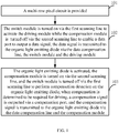
- Embodiments of the present disclosure disclose a pixel circuit driving method, including: providing a plurality of rows of pixel circuits, therein, each row of the pixel circuit includes a switch module, a driving module, a compensation module, an organic light emitting diode, a first scanning line, a second scanning line, and a data compensation line, therein the first scanning line is coupled to the switch module, therein the switch module is further coupled to the driving module, therein the switch module is further coupled to the data compensation line, therein the driving module receives a DC voltage and is coupled to the organic light emitting diode, therein the second scanning line is coupled to the compensation module, and the compensation module is further coupled to the driving module and the organic light emitting diode; each of the plurality of rows of pixel circuits shares an identical data compensation line, and the data compensation line is coupled to the data terminal, the compensation terminal, and the detection terminal of a driving chip; turning on the switch module via the first scanning line to activate the driving module while turning off the compensation module via the second scanning
- the switch module is a first transistor, therein the driving module is a second transistor, and the compensation module is a third transistor; therein the first scanning line is coupled to a gate of the first transistor, therein a drain of the first transistor is coupled to the data compensation line, and the source of the first transistor is coupled to a gate of the second transistor; therein a drain of the second transistor is coupled to a voltage terminal of the driving chip and is configured for receiving the DC voltage; a source of the second transistor is coupled to an anode of the organic light emitting diode, and a cathode of the organic light emitting diode is grounded; therein the second scanning line is coupled to a gate of the third transistor, therein a drain of the third transistor is coupled to the data compensation line, and a source of the third transistor is coupled to an anode of the organic light emitting diode.
- turning on the switch module via the first scanning line to activate the driving module while turning off the compensation module via the second scanning line to enable a data terminal to output a data signal, and transmit the data signal to the organic light emitting diode via the data compensation line, the switch module and the driving module for display includes: outputting a high level signal via the first scanning line and outputting a low level signal via the second scanning line, thus to cut off the third transistor and turn on the first transistor and the second transistor; the data signal outputted by the data terminal is transmitted to the organic light emitting diode via the data compensation line, the switch module and the driving module for display.
- activating the organic light emitting diode, turning on the compensation module via the second scanning line, and turning off the switch module via the first scanning line to perform compensation detection on the organic light emitting diode, based on a determination that the compensation is required, outputting a compensation signal via the compensation terminal, and transmitting the compensation signal to the organic light emitting diode via the data compensation line and the compensation module for performing compensation after detection includes: outputting a high level signal via the first scanning line to turn on the first transistor and the second transistor to activate the organic light emitting diode; outputting a low level signal via the first scanning line to turn on the first transistor and the second transistor is turned off, outputting a high level signal via the second scanning line to turn on the third transistor; detecting a current of the organic light emitting diode via the data compensation line and the third transistor successively; when determining the compensation is required, outputting the compensation signal via the compensation terminal, and transmitting the compensation signal to the organic light emitting diode via the data compensation line and the third transistor for compensating.
- the activating the organic light emitting diode, turning on the compensation module via the second scanning line, and turning off the switch module via the first scanning line to perform compensation detection on the organic light emitting diode, based on a determination that the compensation is required, outputting a compensation signal via a compensation terminal, and transmitting the compensation signal to the organic light emitting diode via the data compensation line and the compensation module for performing compensation after detection includes: outputting a high level signal via the first scanning line to turn on the first transistor and the second transistor to activate the organic light emitting diode; outputting a low level signal via the first scanning line to turn on the first transistor and the second transistor is cut off, outputting a high level signal via the second scanning line to turn on the third transistor; detecting a current of the organic light emitting diode via the data compensation line and the third transistor successively; when determining the compensation is required, outputting the compensation signal via the compensation terminal, and transmitting the compensation signal to the organic light emitting diode via the data compensation line and the third transistor for compensating
- the method before outputting a low level signal via the first scanning line to cut off the first transistor and the second transistor, and outputting a high level signal via the second scanning line to turn on the third transistor; transmitting the data signal outputted via the data terminal to the organic light emitting diode via the data compensation line and the third transistor for activating the organic light emitting diode, the method further includes: outputting a high level signal via the first scanning line to turn on the first transistor, outputting the low level signal via the data terminal and transmitting the low level signal to the second transistor via the data compensation line and the first transistor to cut off the second transistor.
- Embodiments of the present disclosure disclose a pixel circuit group, applied to an organic light emitting display device, therein, the pixel circuit group includes a plurality of rows of pixel circuits; each row of the pixel circuit includes a switch module, a driving module, a compensation module, an organic light emitting diode, a first scanning line, a second scanning line, and a data compensation line; therein the first scanning line is coupled to the switch module, therein the switch module is further coupled to the driving module, therein the switch module is further coupled to the data compensation line, therein the driving module receives a DC voltage and is coupled to the organic light emitting diode, therein the second scanning line is coupled to the compensation module, and the compensation module is further coupled to the driving module and the organic light emitting diode; each of the plurality of rows of pixel circuits shares an identical data compensation line, and the data compensation line is coupled to the data terminal, the compensation terminal, and the detection terminal of a driving chip; during a display phase, the first scanning line is configured to
- the switch module is a first transistor, therein the driving module is a second transistor, and the compensation module is a third transistor; therein the first scanning line is coupled to a gate of the first transistor, therein a drain of the first transistor is coupled to the data compensation line, and the source of the first transistor is coupled to a gate of the second transistor; therein a drain of the second transistor is coupled to a voltage terminal of the driving chip and is configured for receiving the DC voltage, therein a source of the second transistor is coupled to an anode of the organic light emitting diode, and a cathode of the organic light emitting diode is grounded; the second scanning line is coupled to a gate of the third transistor, therein a drain of the third transistor is coupled to the data compensation line, and a source of the third transistor is coupled to an anode of the organic light emitting diode.
- the first scanning line is configured to output a high level signal and the second scanning line is configured to output a low level signal, thus to cut off the third transistor and turn on the first transistor and the second transistor; the data signal outputted by the data terminal is transmitted to the organic light emitting diode via the data compensation line, the switch module and the driving module.
- the first scanning line is configured to output a high level signal to turn on the first transistor and the second transistor is turned on to activate the organic light emitting diode; the first scanning line is further configured to output a low level signal to turn on the first transistor and the second transistor is turned off, therein the second scanning line is configured to output a high level signal to turn on the third transistor to enable a current of the organic light emitting diode transmitted to the compensation terminal via the third transistor and the data compensation line successively for detecting; when determining the compensation is required, compensation terminal is configured to outputs the compensation signal and transmits the compensation signal to the organic light emitting diode via the third transistor for compensating.
- the first scanning line is configured to output a low level signal to cut off the first transistor and the second transistor, the second scanning line is configured to output a high level signal to turn on the third transistor;
- the data terminal is configured to output the data signal and transmit the data signal to the organic light emitting diode via the data compensation line and the third transistor for activating the organic light emitting diode;
- the compensation terminal is configured to detect a current of the organic light emitting diode via the data compensation line and the third transistor; when determining the compensation is required, the compensation terminal is further configured to output the compensation signal and transmit the compensation signal to the organic light emitting diode via the data compensation line and the third transistor.
- the first scanning line is further configured to output a high level signal to turn on the first transistor before output the low level signal
- the data terminal outputs the low level signal and transmits the low level signal to the second transistor via the data compensation line and the first transistor to cut off the second transistor.
- Embodiments of the present disclosure disclose an organic light emitting display device, including a driving chip and a pixel circuit group coupled to the driving chip.
- Embodiments of the present disclosure disclose a pixel circuit driving method, including: providing a plurality of rows of pixel circuits, therein, each row of the pixel circuit includes a switch module, a driving module, a compensation module, an organic light emitting diode, a first scanning line, a second scanning line, and a data compensation line, therein the first scanning line is coupled to the switch module, therein the switch module is further coupled to the driving module, therein the switch module is further coupled to the data compensation line, therein the driving module receives a DC voltage and is coupled to the organic light emitting diode, therein the second scanning line is coupled to the compensation module, and the compensation module is further coupled to the driving module and the organic light emitting diode; each of the plurality of rows of pixel circuits shares an identical data compensation line, and the data compensation line is coupled to the data terminal, the compensation terminal, and the detection terminal of a driving chip; turning on the switch module via the first scanning line to activate the driving module while turning off the compensation module via the second scanning
- the data compensation line is shared by the pixel circuit rather than performing corresponding functions by different lines. Therefore, the pixel circuit reduces the number of lines used in the pixel circuit and greatly improves the pixel effective display aperture ratio and resolution.
- the terms “installation”, “coupled”, and “connected” shall be understood broadly, for example, it can be a fixed connection, or it can be detachably connected, or integrally connected; it can be a mechanical connection; it can be directly connected, or indirectly connected through an intermediary, and it can be the internal connection of two components.
- installation shall be understood broadly, for example, it can be a fixed connection, or it can be detachably connected, or integrally connected; it can be a mechanical connection; it can be directly connected, or indirectly connected through an intermediary, and it can be the internal connection of two components.
- a first embodiment of the first aspect of the present disclosure provides a pixel circuit driving method.
- the pixel circuit driving method includes the following steps.
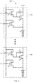
- each row of the pixel circuit 100 includes a switch module Q1, a driving module Q2, a compensation module Q3, an organic light emitting diode D, a first scanning line L1, a second scanning line L2, and a data compensation line P.
- the first scanning line L1 is coupled to the switch module Q1.
- the switch module Q1 is further coupled to the driving module Q2.
- the switch module Q1 is further coupled to the data compensation line P.
- the driving module Q2 receives a DC voltage and is coupled to the organic light emitting diode D.
- the second scanning line L2 is coupled to the compensation module Q3, and the compensation module Q3 is further coupled to the driving module Q2 and the organic light emitting diode D.
- the data compensation lines P of the plurality of rows of pixel circuits are the same one, and the data compensation line P is coupled to the data terminal, the compensation terminal, and the detection terminal.
- the driving module Q2 can be connected with a voltage terminal of a driving chip to receive the DC voltage.
- the switch module Q1 is turned on via the first scanning line L1 to activate the driving module Q2while the compensation module Q3 is turned off via the second scanning line L2, thus to enable the data terminal to output a data signal and transmit the data signal to the organic light emitting diode D via the data compensation line P, the switch module Q1 and the driving module Q2 for display.
- the organic light emitting diode D is in a display stage.
- the organic light emitting diode D being activated, the compensation module Q3being turned on via the second scanning line L2, and the switch module Q1 being turned off via the first scanning line, thus performing compensation detection for the organic light emitting diode D.
- a compensation signal is outputted via the compensation terminal, and the compensation signal is transmitted to the organic light emitting diode D via the data compensation line P and the compensation module Q3 for performing compensation after detection.
- the plurality of rows of pixel circuits are displayed and compensated row by row.
- the plurality of rows of pixel circuits being displayed and compensated row by row means that only after a current row of the pixel circuits is charged for display and compensated may the next row of the pixel circuits be charged for display and compensated.
- the pixel circuit 100 when the organic light emitting diode D is charged for display or compensated, the data compensation line P is shared by the pixel circuit 100 rather than performing corresponding functions by different lines. Therefore, the pixel circuit 100 reduces the number of lines used in the pixel circuit 100 and greatly improves the pixel effective display aperture ratio and resolution.
- the switch module Q1 is a first transistor.
- the driving module Q2 is a second transistor.
- the compensation module Q3 is a third transistor.
- the first scanning line L1 is coupled to a gate of the first transistor, therein a drain of the first transistor is coupled to the data compensation line P, and a source of the first transistor is coupled to a gate of the second transistor; therein a drain of the second transistor is coupled to a voltage terminal of the driving chip and is configured for receiving the DC voltage from the voltage terminal of the driving chip, therein a source of the second transistor is coupled to an anode of the organic light emitting diode D, and a cathode of the organic light emitting diode D is grounded; therein the second scanning line L2 is coupled to a gate of the third transistor, therein a drain of the third transistor is coupled to the data compensation line P, and a source of the third transistor is coupled to an anode of the organic light emitting diode D.
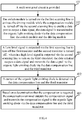
- block 102 includes the following blocks.
- a high level signal is outputted via the first scanning line L1 and a low level signal is outputted via the second scanning line L2, thus to cut off the third transistor and turn on the first transistor and the second transistor.
- the data signal outputted by the data terminal is transmitted to the organic light emitting diode D via the data compensation line P, the switch module Q1 and the driving module Q2 for display.
- the block 103 includes the following blocks.
- a high level signal is outputted via the first scanning line L1 to turn on the first transistor and the second transistor to activate the organic light emitting diode D.
- organic light emitting diode D is activated through the second transistor in this block.
- a low level signal is outputted via the first scanning line L1 to turn on the first transistor and the second transistor is cut off, therein a high level signal is outputted via the second scanning line L2 to turn on the third transistor.
- the detection terminal detects a current of the organic light emitting diode D via the data compensation line P and the third transistor successively.
- the compensation terminal when the compensation is determined to be required, the compensation terminal outputs the compensation signal, and transmits the compensation signal to the organic light emitting diode D via the data compensation line P and the third transistor for compensating.
- the driving chip can determine the current offset of the organic light emitting diode D activated by the second transistor according to the current of the organic light emitting diode D received through the detection terminal, and control the compensation terminal output the compensation signal.
- the compensation signal is transmitted to the organic light emitting diode D via the data compensation line P to adjust the current of the organic light emitting diode D to a preset current to achieve compensation.
- the first to third transistors are thin film transistors.
- a second embodiment of the present disclosure provides a pixel circuit driving method.
- the pixel circuit driving method provided by the second embodiment is similar to the pixel circuit driving method provided by the first embodiment (that is, blocks 101-102 are the same). The differences are as follows: the block of "the organic light emitting diode D being activated, the compensation module Q3 being turned on via the second scanning line L2, and the switch module Q1 being cut off via the first scanning line L1, thus to perform compensation detection on the organic light emitting diode D. Based on a determination that the compensation is required, the compensation signal is outputted via a compensation terminal, and transmitted to the organic light emitting diode D via the data compensation line P and the compensation module Q3 for performing compensation after detection" includes the following blocks.
- a low level signal is outputted via the first scanning line L1 to cut off the first transistor and the second transistor; a high level signal is outputted via the second scanning line L2 to turn on the third transistor; the data terminal outputs the data signal, and transmits the data signal to the organic light emitting diode D via the data compensation line P and the third transistor to activate the organic light emitting diode D.
- the current of the organic light emitting diode D is detected via the data compensation line P and the third transistor.
- the compensation terminal outputs the compensation signal, and transmits the compensation signal to the organic light emitting diode D via the data compensation line P and the third transistor.
- the driving chip can determine the current offset of the organic light emitting diode D activated by the second transistor according to the current of the organic light emitting diode D received through the detection terminal, and control the compensation terminal output the compensation signal.
- the compensation signal is transmitted to the organic light emitting diode D via the data compensation line P to adjust the current of the organic light emitting diode D to a preset current to achieve compensation.
- the high level signal is outputted via the first scanning line to turn on the first transistor.
- the data terminal outputs the low level signal and transmits the low level signal to the second transistor via the data compensation line and the first transistor to cut off the second transistor.
- the pixel circuit driving method provided by the present disclosure is also applicable to a liquid crystal display device.
- a first embodiment of the second aspect of the present disclosure provides a pixel circuit group 200.
- the pixel circuit group 200 is applied to an organic light emitting display device.
- the pixel circuit group 200 includes a plurality of rows of pixel circuits 100.each row of the pixel circuit 100includes a switch module 10, a driving module 20, a compensation module 30, an organic light emitting diode D, a first scanning line L1, a second scanning line L2, and a data compensation line P.
- the first scanning line L1 is coupled to the switch module Q1.
- the switch module Q1 is further coupled to the driving module Q2.
- the switch module Q1 is further coupled to the data compensation line P.
- the driving module Q2 receives a DC voltage and is coupled to the organic light emitting diode D.
- the second scanning line L2 is coupled to the compensation module Q3, and the compensation module Q3 is further coupled to the driving module Q2 and the organic light emitting diode D.
- the data compensation lines of a plurality of rows of pixel circuits are the same one, and the data compensation lines are coupled to the data terminal, the compensation terminal, and the detection terminal of a driving chip.
- the first scanning line L1 is configured to turn on the switch module Q1 to activate the driving module D.
- the second scanning line L2 is configured to turn off the compensation module Q3 to enable a data terminal to output a data signal and transmits the data signal to the organic light emitting diode D via the data compensation line P, the switch module Q1 and the driving module Q2.
- the organic light emitting diode D being activated, the second scanning line L2 being configured to turn on the compensation module Q3, and the first scanning line L1 being configured to turn off the switch module Q1, thus to perform compensation detection on the organic light emitting diode D.
- the compensation terminal Based on a determination that the compensation is required, the compensation terminal outputs the compensation signal, and transmits the compensation signal to the organic light emitting diode D via the data compensation line P and the compensation module Q3. Therein, a plurality of rows of pixel circuits are displayed and compensated row by row.
- the driving module Q2 can be connected with a voltage terminal of a driving chip to receive the DC voltage.
- the plurality of rows of pixel circuits being displayed and compensated row by row means that only after a current row of the pixel circuits is charged for display may a next row of the pixel circuits be charged for display and compensated.
- the pixel circuit 100 when the organic light emitting diode D is charged for display or compensated, the data compensation line P is shared, rather than performing corresponding functions by different lines. Therefore, the pixel circuit 100 reduces the number of lines used in the pixel circuit 100 and greatly improves the pixel effective display aperture ratio and resolution.
- the switch module Q1 is a first transistor.
- the driving module Q2 is a second transistor.
- the compensation module Q3 is a third transistor.
- the first scanning line L1 is coupled to a gate of the first transistor, therein a drain of the first transistor is coupled to the data compensation line P, and the source of the first transistor is coupled to a gate of the second transistor; therein a drain of the second transistor is coupled to a voltage terminal of the driving chip and is configured for receiving the DC voltage, therein a source of the second transistor is coupled to an anode of the organic light emitting diode D, and a cathode of the organic light emitting diode D is grounded; therein the second scanning line L2 is coupled to a gate of the third transistor, therein a drain of the third transistor is coupled to the data compensation line P, and a source of the third transistor is coupled to an anode of the organic light emitting diode D.
- the first scanning line L1 is configured to output a high level signal to turn on the first transistor and the second transistor, therein the second scanning line L2 is configured to output a low level signal to cut off the third transistor.
- the data signal outputted by the data terminal is transmitted to the organic light emitting diode D via the data compensation line P, the switch module Q1 and the driving module Q2.
- the first scanning line L1 is configured to output a high level signal to turn on the first transistor and the second transistor is turned on to activate the organic light emitting diode D.
- the first scanning line L1 is further configured to output a low level signal to turn on the first transistor and the second transistor is cut off, therein the second scanning line L2 is configured to output a high level signal to turn on the third transistor to enable a current of the organic light emitting diode D transmitted to the compensation terminal via the third transistor and the data compensation line P successively for detecting.
- the compensation terminal is configured to outputs the compensation signal and transmits the compensation signal to the organic light emitting diode D via the third transistor for compensating.
- the first scanning line L1 activate the organic light emitting diode D through the second transistor.
- the driving chip can determine the current offset of the organic light emitting diode D activated by the second transistor according to the current of the organic light emitting diode D received through the detection terminal, and control the compensation terminal output the compensation signal.
- the compensation signal is transmitted to the organic light emitting diode D via the data compensation line P to adjust the current of the organic light emitting diode D to a preset current to achieve compensation.
- the organic light emitting diode D can also be activated by the third transistor, that is, during the compensation phase after detection, the first scanning line L1 is configured to output a low level signal to cut off the first transistor and the second transistor, therein the second scanning line L2 is configured to output a high level signal to turn on the third transistor.
- the data terminal is configured to output the data signal and transmit the data signal to the organic light emitting diode D via the data compensation line P and the third transistor for activating the organic light emitting diode D.
- the compensation terminal is configured to detect a current of the organic light emitting diode D via the data compensation line P and the third transistor. When the compensation is determined to be required, the compensation terminal is further configured to output the compensation signal and transmit the compensation signal to the organic light emitting diode D via the data compensation line P and the third transistor.
- the driving chip can determine the current offset of the organic light emitting diode D activated by the second transistor according to the current of the organic light emitting diode D received through the detection terminal, and control the compensation terminal output the compensation signal.
- the compensation signal is transmitted to the organic light emitting diode D via the data compensation line P to adjust the current of the organic light emitting diode D to a preset current to achieve compensation.
- the first scan line L1 is further configured to output a high level signal to turn on the first transistor before output a low level signal
- the data terminal is further configured to output a low level signal which transmitted to the second transistor via the data compensation line P and the first transistor to cut off the second transistor.
- the pixel circuit group 200 can also be applied to a liquid crystal display device.
- a third aspect of the present disclosure provides an organic light emitting display device 500.
- the organic light emitting display device includes a driving chip 510 and the above described pixel circuit group 200 connected with the driving chip 510.
- the above pixel circuit group 200 has been described in detail in the above second embodiment, it will not be described herein.
- the organic light emitting display device 500 includes the pixel circuit 100.
- the pixel circuit 100 when the organic light emitting diode D is charged for display or compensated, the data compensation line P is shared, rather than performing the corresponding functions by different lines. Therefore, the pixel circuit 100 reduces the number of lines used in the pixel circuit 100 and greatly improves the pixel effective display aperture ratio and resolution.
Landscapes
- Engineering & Computer Science (AREA)
- Physics & Mathematics (AREA)
- Computer Hardware Design (AREA)
- General Physics & Mathematics (AREA)
- Theoretical Computer Science (AREA)
- Chemical & Material Sciences (AREA)
- Crystallography & Structural Chemistry (AREA)
- Electroluminescent Light Sources (AREA)
- Control Of El Displays (AREA)
- Control Of Indicators Other Than Cathode Ray Tubes (AREA)
Applications Claiming Priority (1)
| Application Number | Priority Date | Filing Date | Title |
|---|---|---|---|
| PCT/CN2016/112344 WO2018119650A1 (zh) | 2016-12-27 | 2016-12-27 | 像素电路驱动方法、像素电路组及有机发光显示设备 |
Publications (2)
| Publication Number | Publication Date |
|---|---|
| EP3564940A1 true EP3564940A1 (de) | 2019-11-06 |
| EP3564940A4 EP3564940A4 (de) | 2020-06-10 |
Family
ID=62004243
Family Applications (1)
| Application Number | Title | Priority Date | Filing Date |
|---|---|---|---|
| EP16925410.9A Withdrawn EP3564940A4 (de) | 2016-12-27 | 2016-12-27 | Ansteuerungsverfahren für pixelschaltung, pixelschaltungsgruppe und organische lichtemittierende anzeigevorrichtung |
Country Status (6)
| Country | Link |
|---|---|
| US (1) | US10930214B2 (de) |
| EP (1) | EP3564940A4 (de) |
| JP (1) | JP6910444B2 (de) |
| KR (1) | KR102241717B1 (de) |
| CN (1) | CN107980159B (de) |
| WO (1) | WO2018119650A1 (de) |
Families Citing this family (7)
| Publication number | Priority date | Publication date | Assignee | Title |
|---|---|---|---|---|
| CN108877651B (zh) * | 2017-05-12 | 2020-12-22 | 京东方科技集团股份有限公司 | 显示面板、显示设备及补偿方法 |
| US11170718B2 (en) | 2017-05-12 | 2021-11-09 | Boe Technology Group Co., Ltd. | Display panel, display device and compensating method |
| CN109801597B (zh) * | 2019-02-27 | 2020-12-25 | 深圳市华星光电半导体显示技术有限公司 | 显示器驱动电路及显示器驱动方法 |
| CN109742134B (zh) | 2019-03-15 | 2022-07-05 | 合肥京东方卓印科技有限公司 | 有机发光二极管显示装置及其驱动方法 |
| CN110010064B (zh) * | 2019-04-19 | 2020-09-22 | Oppo广东移动通信有限公司 | 像素驱动电路、显示屏及电子设备 |
| CN111028782A (zh) * | 2020-01-09 | 2020-04-17 | 深圳市华星光电半导体显示技术有限公司 | 像素电路和具有该像素电路的显示装置 |
| KR102922922B1 (ko) * | 2022-07-27 | 2026-02-04 | 삼성전자주식회사 | 디스플레이 장치 및 이의 제어 방법 |
Family Cites Families (27)
| Publication number | Priority date | Publication date | Assignee | Title |
|---|---|---|---|---|
| TW200534202A (en) * | 2004-04-09 | 2005-10-16 | Toppoly Optoelectronics Corp | Active matrix oled pixel structure and driving method thereof |
| KR100858615B1 (ko) * | 2007-03-22 | 2008-09-17 | 삼성에스디아이 주식회사 | 유기전계발광 표시장치 및 그의 구동방법 |
| KR100893482B1 (ko) * | 2007-08-23 | 2009-04-17 | 삼성모바일디스플레이주식회사 | 유기전계발광 표시장치 및 그의 구동방법 |
| KR101416904B1 (ko) * | 2007-11-07 | 2014-07-09 | 엘지디스플레이 주식회사 | 유기전계발광 표시장치의 화소 구동 장치 |
| JP2010160386A (ja) * | 2009-01-09 | 2010-07-22 | Seiko Epson Corp | 発光装置、電子機器および発光装置の制御方法 |
| KR101056317B1 (ko) * | 2009-04-02 | 2011-08-11 | 삼성모바일디스플레이주식회사 | 화소 및 이를 이용한 유기전계발광 표시장치 |
| JP2011095720A (ja) * | 2009-09-30 | 2011-05-12 | Casio Computer Co Ltd | 発光装置及びその駆動制御方法、並びに電子機器 |
| KR101388286B1 (ko) * | 2009-11-24 | 2014-04-22 | 엘지디스플레이 주식회사 | 유기발광다이오드 표시장치 및 그 구동방법 |
| KR101147427B1 (ko) * | 2010-03-02 | 2012-05-22 | 삼성모바일디스플레이주식회사 | 유기 발광 표시 장치 및 그의 구동 방법 |
| EP2715711A4 (de) * | 2011-05-28 | 2014-12-24 | Ignis Innovation Inc | System und verfahren zur schnellen kompensationsprogrammierung von pixeln auf einer anzeige |
| CN103680391B (zh) * | 2012-09-17 | 2016-01-13 | 群康科技(深圳)有限公司 | 显示装置及其调光方法 |
| KR102025120B1 (ko) * | 2013-05-24 | 2019-09-26 | 삼성디스플레이 주식회사 | 보상부 및 이를 포함한 유기 전계 발광 표시 장치 |
| JP6129318B2 (ja) * | 2013-07-30 | 2017-05-17 | シャープ株式会社 | 表示装置およびその駆動方法 |
| KR102159390B1 (ko) * | 2013-11-13 | 2020-09-24 | 삼성디스플레이 주식회사 | 유기전계발광 표시장치 및 그의 구동방법 |
| JP2015102804A (ja) * | 2013-11-27 | 2015-06-04 | 三星ディスプレイ株式會社Samsung Display Co.,Ltd. | 表示装置、および制御方法 |
| JP6169191B2 (ja) * | 2013-12-20 | 2017-07-26 | シャープ株式会社 | 表示装置およびその駆動方法 |
| JP2015156002A (ja) * | 2014-02-21 | 2015-08-27 | 三星ディスプレイ株式會社Samsung Display Co.,Ltd. | 表示装置、および制御方法 |
| KR20150100997A (ko) * | 2014-02-24 | 2015-09-03 | 삼성디스플레이 주식회사 | 유기전계발광 표시장치 |
| US9728125B2 (en) * | 2014-12-22 | 2017-08-08 | Shenzhen China Star Optoelectronics Technology Co., Ltd | AMOLED pixel circuit |
| WO2016125641A1 (ja) * | 2015-02-03 | 2016-08-11 | シャープ株式会社 | 表示装置およびその駆動方法 |
| WO2016129463A1 (ja) * | 2015-02-10 | 2016-08-18 | シャープ株式会社 | 表示装置およびその駆動方法 |
| KR102285393B1 (ko) * | 2015-03-13 | 2021-08-04 | 삼성디스플레이 주식회사 | 유기 발광 표시 장치 및 이의 구동 방법 |
| CN104778922B (zh) * | 2015-04-28 | 2017-12-12 | 温州洪启信息科技有限公司 | 一种amoled像素驱动电路及其驱动方法 |
| CN105047137B (zh) * | 2015-09-09 | 2017-05-31 | 深圳市华星光电技术有限公司 | Amoled实时补偿系统 |
| CN205751477U (zh) * | 2016-05-12 | 2016-11-30 | 上海锦荃电子科技有限公司 | 有机发光显示器的像素驱动电路 |
| CN105913802B (zh) * | 2016-06-30 | 2018-09-21 | 上海天马有机发光显示技术有限公司 | 一种有机电致发光二极管显示面板及其驱动方法 |
| CN105957473B (zh) * | 2016-06-30 | 2019-03-08 | 上海天马有机发光显示技术有限公司 | 一种有机发光显示面板及其驱动方法 |
-
2016
- 2016-12-27 WO PCT/CN2016/112344 patent/WO2018119650A1/zh not_active Ceased
- 2016-12-27 CN CN201680042992.1A patent/CN107980159B/zh not_active Expired - Fee Related
- 2016-12-27 JP JP2019531956A patent/JP6910444B2/ja not_active Expired - Fee Related
- 2016-12-27 KR KR1020197020132A patent/KR102241717B1/ko not_active Expired - Fee Related
- 2016-12-27 EP EP16925410.9A patent/EP3564940A4/de not_active Withdrawn
-
2019
- 2019-06-17 US US16/442,935 patent/US10930214B2/en not_active Expired - Fee Related
Also Published As
| Publication number | Publication date |
|---|---|
| KR20190092535A (ko) | 2019-08-07 |
| JP6910444B2 (ja) | 2021-07-28 |
| WO2018119650A1 (zh) | 2018-07-05 |
| CN107980159B (zh) | 2021-06-29 |
| JP2020502574A (ja) | 2020-01-23 |
| KR102241717B1 (ko) | 2021-04-16 |
| EP3564940A4 (de) | 2020-06-10 |
| US20190304369A1 (en) | 2019-10-03 |
| CN107980159A (zh) | 2018-05-01 |
| US10930214B2 (en) | 2021-02-23 |
Similar Documents
| Publication | Publication Date | Title |
|---|---|---|
| US10930214B2 (en) | Pixel circuit driving method, pixel circuit group and organic light emitting display device improving display aperture ratio and resolution | |
| KR102007614B1 (ko) | Amoled 실시간 보상 시스템 | |
| US10565909B2 (en) | Test method for display panel, and test device | |
| US8063857B2 (en) | Image display apparatus | |
| US11769452B2 (en) | Display panel, method for driving the same, and display apparatus | |
| EP3038079B1 (de) | Überstromsteuerungsvorrichtung und organische lichtemittierende anzeigevorrichtung damit | |
| US20200365087A1 (en) | Voltage drop compensation system and method for power supply inside display panel | |
| US10643536B2 (en) | Pixel circuit and driving method thereof, display panel | |
| US8125417B2 (en) | Display driver circuit for driving a light-emitting device with the threshold offset of a drive transistor compensated for | |
| CN109935205B (zh) | 像素驱动电路以及像素驱动电路的补偿方法 | |
| WO2017197702A1 (zh) | Oled显示装置的阈值电压侦测电路 | |
| US10622424B2 (en) | Pixel circuit and driving method thereof, display panel | |
| US9928783B2 (en) | Power control device and method and organic light emitting display device including the same | |
| CN107274832B (zh) | 驱动电路及显示装置 | |
| US11037510B2 (en) | Pixel driving system for AMOLED display device and driving method | |
| US20190043424A1 (en) | AMOLED Display Panel with Function of Temperature Compensation and Display Device Thereof | |
| US7450094B2 (en) | Light emitting device and method of driving the same | |
| US20200027392A1 (en) | Driving system of amoled display panel and amoled display panel | |
| US20160069947A1 (en) | Method and apparatus for testing display panel | |
| US20190057982A1 (en) | Flexible display and improving method and improving device of bending display abnormality thereof | |
| KR20210040588A (ko) | 표시장치 및 그의 구동방법 | |
| US9262959B2 (en) | EL display device | |
| US11881174B2 (en) | OLED drive circuit for detecting and compensating data voltage | |
| US10049630B2 (en) | Image correcting unit and a liquid crystal display device having the same | |
| US10573241B2 (en) | Driving circuit and display device |
Legal Events
| Date | Code | Title | Description |
|---|---|---|---|
| STAA | Information on the status of an ep patent application or granted ep patent |
Free format text: STATUS: THE INTERNATIONAL PUBLICATION HAS BEEN MADE |
|
| PUAI | Public reference made under article 153(3) epc to a published international application that has entered the european phase |
Free format text: ORIGINAL CODE: 0009012 |
|
| STAA | Information on the status of an ep patent application or granted ep patent |
Free format text: STATUS: REQUEST FOR EXAMINATION WAS MADE |
|
| 17P | Request for examination filed |
Effective date: 20190612 |
|
| AK | Designated contracting states |
Kind code of ref document: A1 Designated state(s): AL AT BE BG CH CY CZ DE DK EE ES FI FR GB GR HR HU IE IS IT LI LT LU LV MC MK MT NL NO PL PT RO RS SE SI SK SM TR |
|
| AX | Request for extension of the european patent |
Extension state: BA ME |
|
| DAV | Request for validation of the european patent (deleted) | ||
| DAX | Request for extension of the european patent (deleted) | ||
| REG | Reference to a national code |
Ref country code: DE Ref legal event code: R079 Free format text: PREVIOUS MAIN CLASS: G09G0003360000 Ipc: G09G0003323300 |
|
| A4 | Supplementary search report drawn up and despatched |
Effective date: 20200512 |
|
| RIC1 | Information provided on ipc code assigned before grant |
Ipc: G09G 3/3233 20160101AFI20200506BHEP |
|
| STAA | Information on the status of an ep patent application or granted ep patent |
Free format text: STATUS: EXAMINATION IS IN PROGRESS |
|
| 17Q | First examination report despatched |
Effective date: 20210924 |
|
| STAA | Information on the status of an ep patent application or granted ep patent |
Free format text: STATUS: THE APPLICATION IS DEEMED TO BE WITHDRAWN |
|
| 18D | Application deemed to be withdrawn |
Effective date: 20230701 |