EP3563447B1 - Verbindungssystem für eine mehrlagige hochfrequenzschaltung und verfahren zur herstellung - Google Patents
Verbindungssystem für eine mehrlagige hochfrequenzschaltung und verfahren zur herstellung Download PDFInfo
- Publication number
- EP3563447B1 EP3563447B1 EP17829883.2A EP17829883A EP3563447B1 EP 3563447 B1 EP3563447 B1 EP 3563447B1 EP 17829883 A EP17829883 A EP 17829883A EP 3563447 B1 EP3563447 B1 EP 3563447B1
- Authority
- EP
- European Patent Office
- Prior art keywords
- stripline
- board
- dielectric substrate
- printed circuit
- over
- Prior art date
- Legal status (The legal status is an assumption and is not a legal conclusion. Google has not performed a legal analysis and makes no representation as to the accuracy of the status listed.)
- Active
Links
Images


Classifications
-
- H—ELECTRICITY
- H01—ELECTRIC ELEMENTS
- H01P—WAVEGUIDES; RESONATORS, LINES, OR OTHER DEVICES OF THE WAVEGUIDE TYPE
- H01P3/00—Waveguides; Transmission lines of the waveguide type
- H01P3/02—Waveguides; Transmission lines of the waveguide type with two longitudinal conductors
- H01P3/08—Microstrips; Strip lines
- H01P3/085—Triplate lines
-
- H—ELECTRICITY
- H01—ELECTRIC ELEMENTS
- H01P—WAVEGUIDES; RESONATORS, LINES, OR OTHER DEVICES OF THE WAVEGUIDE TYPE
- H01P3/00—Waveguides; Transmission lines of the waveguide type
- H01P3/02—Waveguides; Transmission lines of the waveguide type with two longitudinal conductors
- H01P3/08—Microstrips; Strip lines
-
- H—ELECTRICITY
- H01—ELECTRIC ELEMENTS
- H01P—WAVEGUIDES; RESONATORS, LINES, OR OTHER DEVICES OF THE WAVEGUIDE TYPE
- H01P5/00—Coupling devices of the waveguide type
- H01P5/02—Coupling devices of the waveguide type with invariable factor of coupling
- H01P5/022—Transitions between lines of the same kind and shape, but with different dimensions
- H01P5/028—Transitions between lines of the same kind and shape, but with different dimensions between strip lines
-
- H—ELECTRICITY
- H05—ELECTRIC TECHNIQUES NOT OTHERWISE PROVIDED FOR
- H05K—PRINTED CIRCUITS; CASINGS OR CONSTRUCTIONAL DETAILS OF ELECTRIC APPARATUS; MANUFACTURE OF ASSEMBLAGES OF ELECTRICAL COMPONENTS
- H05K1/00—Printed circuits
- H05K1/02—Details
- H05K1/0213—Electrical arrangements not otherwise provided for
- H05K1/0216—Reduction of cross-talk, noise or electromagnetic interference
- H05K1/0218—Reduction of cross-talk, noise or electromagnetic interference by printed shielding conductors, ground planes or power plane
- H05K1/0219—Printed shielding conductors for shielding around or between signal conductors, e.g. coplanar or coaxial printed shielding conductors
-
- H—ELECTRICITY
- H05—ELECTRIC TECHNIQUES NOT OTHERWISE PROVIDED FOR
- H05K—PRINTED CIRCUITS; CASINGS OR CONSTRUCTIONAL DETAILS OF ELECTRIC APPARATUS; MANUFACTURE OF ASSEMBLAGES OF ELECTRICAL COMPONENTS
- H05K3/00—Apparatus or processes for manufacturing printed circuits
- H05K3/40—Forming printed elements for providing electric connections to or between printed circuits
- H05K3/403—Edge contacts; Windows or holes in the substrate having plural connections on the walls thereof
-
- H—ELECTRICITY
- H05—ELECTRIC TECHNIQUES NOT OTHERWISE PROVIDED FOR
- H05K—PRINTED CIRCUITS; CASINGS OR CONSTRUCTIONAL DETAILS OF ELECTRIC APPARATUS; MANUFACTURE OF ASSEMBLAGES OF ELECTRICAL COMPONENTS
- H05K1/00—Printed circuits
- H05K1/02—Details
- H05K1/0213—Electrical arrangements not otherwise provided for
- H05K1/0237—High frequency adaptations
- H05K1/025—Impedance arrangements, e.g. impedance matching, reduction of parasitic impedance
-
- H—ELECTRICITY
- H05—ELECTRIC TECHNIQUES NOT OTHERWISE PROVIDED FOR
- H05K—PRINTED CIRCUITS; CASINGS OR CONSTRUCTIONAL DETAILS OF ELECTRIC APPARATUS; MANUFACTURE OF ASSEMBLAGES OF ELECTRICAL COMPONENTS
- H05K1/00—Printed circuits
- H05K1/02—Details
- H05K1/14—Structural association of two or more printed circuits
- H05K1/144—Stacked arrangements of planar printed circuit boards
-
- H—ELECTRICITY
- H05—ELECTRIC TECHNIQUES NOT OTHERWISE PROVIDED FOR
- H05K—PRINTED CIRCUITS; CASINGS OR CONSTRUCTIONAL DETAILS OF ELECTRIC APPARATUS; MANUFACTURE OF ASSEMBLAGES OF ELECTRICAL COMPONENTS
- H05K2201/00—Indexing scheme relating to printed circuits covered by H05K1/00
- H05K2201/09—Shape and layout
- H05K2201/09145—Edge details
-
- H—ELECTRICITY
- H05—ELECTRIC TECHNIQUES NOT OTHERWISE PROVIDED FOR
- H05K—PRINTED CIRCUITS; CASINGS OR CONSTRUCTIONAL DETAILS OF ELECTRIC APPARATUS; MANUFACTURE OF ASSEMBLAGES OF ELECTRICAL COMPONENTS
- H05K2201/00—Indexing scheme relating to printed circuits covered by H05K1/00
- H05K2201/09—Shape and layout
- H05K2201/09145—Edge details
- H05K2201/0919—Exposing inner circuit layers or metal planes at the side edge of the printed circuit board [PCB] or at the walls of large holes
-
- H—ELECTRICITY
- H05—ELECTRIC TECHNIQUES NOT OTHERWISE PROVIDED FOR
- H05K—PRINTED CIRCUITS; CASINGS OR CONSTRUCTIONAL DETAILS OF ELECTRIC APPARATUS; MANUFACTURE OF ASSEMBLAGES OF ELECTRICAL COMPONENTS
- H05K3/00—Apparatus or processes for manufacturing printed circuits
- H05K3/46—Manufacturing multilayer circuits
Definitions
- a via refers to an electrical connection between layers in a radio frequency (RF) circuit which passes through the plane of one or more adjacent layers of a printed circuit board (PCB).
- RF radio frequency
- PCB printed circuit board
- a via may include a hole or opening formed in the PCB with a conductor disposed or otherwise provided in the opening to provide an electrically conductive pathway from one end of the opening to the other.
- a via electrically connects the different layers using a hole formed through the respective boards.
- the vias can take up valuable space within the PCB.
- the vias may be prone to leaks resulting in areas of high field density around the location of the respective via. Thus, unrestricted fields can propagate throughout the individual layers impacting a performance of the respective PCB.
- An element housing package and mounting structure body are known from US2015173214A1 .
- Electromagnetic wave propagation path and electromagnetic wave propagation device are known from US2014/0167882A1 .
- Documents US 2005/098348 A1 (OKUMICHI TAKEHIRO [JP] ET AL) 12 May 2005 (2005-05-12) and US 2009/000106 A1 (CHUANG CHIA-CHENG [TW] ET AL) 1 January 2009 (2009-01-01) discloses vertical interconnections between layers of a common multilayer board.
- interconnect to couple different layers of a multilayered radio frequency (RF) circuit, such as a multilayered printed circuit board (PCB).
- RF radio frequency
- PCB printed circuit board
- the interconnect may be formed along an outer surface of one or more stripline boards making up the multilayered PCB to electrically couple conductors on the respective stripline boards.
- the interconnect can electrically couple conductors disposed on different layers of the multilayered PCB without using holes formed through the different layers.
- center conductors of stripline transmission lines provided on respective ones of multiple stripline boards may be electrically coupled via an interconnect formed or otherwise disposed over an edge or side portion of dielectric layers of the multiple stripline boards such that the interconnect extends at least from a first center conductor in a first stripline board to a second center conductor in a second stripline board.
- the interconnect may be printed onto an outer surface or edge or side portion of a stripline board using additive manufacturing techniques.
- An electrically conductive wall may be formed over the edge or side portion of dielectric layers which form the stripline board to form a cavity that encloses the interconnect and the outer surface of the multilayered PCB.
- the cavity may be air-filled or filled with dielectric material.
- the conductive wall may be formed in a variety of different shapes or designs based at least in part on the location and/or dimensions of the interconnect.
- the conductive wall may electrically isolate the interconnect from surrounding circuitry in the multilayered PCB, thereby preventing undesirable coupling of signals from "leaking" between signals paths (i.e., the conductive wall helps support and ideally eliminates "leakage” signals).
- the interconnect may allow for high isolation between adjacent stripline boards and minimize system losses.
- the interconnect systems and methods as described herein enable design and manufacture of high-performance apertures.
- the low loss may allow a smaller sized array to be utilized for particular applications.
- the multilayered PCB may operate at a wide radar bandwidth.
- the interconnect may be formed using additive manufacturing techniques.
- the interconnect can be directly printed onto portions of an outer surface of the respective multilayered PCB.
- Additive manufacturing and the elimination of vias within the multilayered PCB may provide for cost savings, thus, reducing manufacturing costs as compared to PCB designs having conductive vias.
- the systems and methods described herein may enable additive manufactured phased arrays.
- Claim 1 discloses the concepts sought to be protected herein.
- the first stripline board may include a first dielectric substrate disposed over a first surface of the first conductor and a second dielectric substrate disposed over a second surface of the first conductor and a first ground plane formed over a first surface of the first dielectric substrate.
- the conductive layer may be formed over a second surface of the second dielectric substrate to form a second ground plane of the first stripline board.
- the second stripline board may include a first dielectric substrate disposed over a first surface of the second conductor and a second dielectric substrate disposed over a second surface of the second conductor and a first ground plane formed over a second surface of the second dielectric substrate.
- the conductive layer may be formed over a first surface of the first dielectric substrate to form a second ground plane of the second stripline board.
- the interconnect can be formed along an outer surface of a second dielectric substrate of the first stripline board and an outer surface of a first dielectric substrate of the second stripline board.
- the outer surface of the second dielectric substrate of the first stripline board and the outer surface of the first dielectric substrate of the second stripline board are substantially flush.
- the first stripline board and the second stripline board are different lengths such that the outer surface of the second dielectric substrate of the first stripline board and the outer surface of the first dielectric substrate of the second stripline board form a step shaped surface.
- One or more ramps may be formed over one or more ground planes within the multilayered printed circuit board.
- the interconnect can be disposed over the one or more ramps to couple the first and second conductor over the step shaped surface.
- the electrically conductive wall can be coupled to the first surface of the first stripline board and the second surface of the second stripline board.
- the electrically conductive wall can enclose the outer surface such that the cavity is formed between the outer surface of the first and second stripline boards and an inner surface of the electrically conductive wall.
- Dielectric material may be disposed within the cavity.
- a first dielectric substrate can be disposed over a first surface of the first conductor, a second dielectric substrate can be disposed over a second surface of the first conductor and a first ground plane can be formed over a first surface of the first dielectric substrate.
- a second ground plane can be formed over a second surface of the second dielectric substrate using the conductive layer.
- the method may further comprise disposing a first dielectric substrate over a first surface of the second conductor and a second dielectric substrate over a second surface of the second conductor and forming a first ground plane over a second surface of the second dielectric substrate.
- a second ground plane may be formed over a first surface of the first dielectric substrate using the conductive layer.
- the interconnect can be disposed along an outer surface of a second dielectric substrate of the first stripline board and an outer surface of a first dielectric substrate of the second stripline board.
- first stripline board and the second stripline board can be provided at different lengths such that the outer surface of the second dielectric substrate of the first stripline board and the outer surface of the first dielectric substrate of the second stripline board form a step shaped surface.
- One or more ramps may be formed over one or more ground planes within the multilayered printed circuit board and the interconnect may be disposed over the one or more ramps to couple the first and second conductor over the step shaped surface.
- the method may further comprise coupling the electrically conductive wall to the first surface of the first stripline board and the second surface of the second stripline board.
- a cavity may be formed between the outer surface of the first and second stripline boards and an inner surface of the electrically conductive wall and dielectric material can be disposed within the cavity.
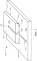
- a multilayered printed circuit board (PCB) 100 includes a first and second stripline transmission line boards 102, 104 with first stripline board 102 provided from a pair of dielectric substrates 110, 112 having conductive ground planes 106, 130 disposed on outer surfaces 110a, 112b thereof Second stripline board 104 is provided from a pair of dielectric substrates 114, 116 having conductive ground planes 108, 130 disposed on outer surfaces 114a, 116b thereof.
- conductive layer 130 is disposed between first and second stripline boards 102, 104 and serves as a ground plane for both stripline circuit boards 102, 104 (i.e., a shaped ground plane).
- a bonding layer (not visible in FIG. 1 ) may be disposed between first and second stripline boards 102, 104, and between stripline layers 110, 112 and 114, 116.
- conductive layer 130 may be provided as part of substrate 112 (e.g., disposed on surfaces 112b) and a bond film or other bond material may be disposed between ground plane 130 and surface 114a of substrate 114.
- first and second stripline boards 102, 104 may be bonded together, in a variety of different techniques, as is generally known.
- First stripline board 102 includes a first conductor 122 (shown here in phantom) disposed between dielectric substrates 110, 112. Conductor 122 thus corresponds to a stripline transmission line with conductors 106, 130 corresponding to ground planes.
- Second stripline board 104 includes a second conductor 124 (shown here in phantom) disposed between dielectric substrates 114, 116. Second conductor 124 corresponds to a second stripline transmission line with conductors 108, 130 corresponding to ground planes.
- Interconnect 120 couples first conductor 122 to second conductor 124.
- Interconnect 120 can be disposed along portions of outer surfaces 102c, 104c of first and second stripline boards 102,104.
- interconnect 120 can be disposed over an outer surface 112c of second dielectric substrate 112 of first stripline board 102 and an outer surface 114c of first dielectric substrate 114 of second stripline board 104.
- interconnect 120 can be formed along one side or edge of multilayered PCB 100.
- a cut-out 132 may be formed on an edge 130c (e.g., side portion) of conductive layer 130 to ensure that interconnect 120 does not contact conductive layer 130.
- edge 130c e.g., side portion
- a portion of interconnect 120 may pass by edge 130c of conductive layer 130.
- Cut-out 132 may be formed along edge 130c such that it is adjacent to the portion of interconnect 120 that passes by edge 130c.
- the dimensions (e.g., width, length) of cut-out 132 can correspond to the dimensions (e.g., width, length) and be selected such that interconnect 120 does not contact conductive layer 130.
- cut-out 132 may be filled with dielectric material and interconnect 120 may be formed on or otherwise disposed over the dielectric material within cut-out 132.
- Interconnect 120 may be provided having dimensions suitable to couple radio frequency (RF) signals between the first and second conductors 122, 124, of first and second stripline boards 102, 104 respectively.
- first and second conductors 122, 124 correspond to center conductors of stripline transmission lines provided in the first and second stripline boards 102, 104 respectively along which RF signals may propagate.
- Interconnect 120 may be provided from any suitable conductive material or otherwise disposed or otherwise provided on surfaces of dielectric substrates 110, 112, 114, 116.
- interconnect 120 can be disposed onto a surface of one or more dielectric substrates 110, 112, 114, 116 using pick and place machines and techniques.
- interconnect 120 may be printed onto a surface of one or more dielectric substrates 110, 112, 114, 116 using additive manufacturing techniques.
- interconnect 120 may include various types of conductive inks that may be printed onto the exposed conductors and dielectric surfaces.
- Interconnect 120 may be referred to herein as a vertical interconnect.
- vertical interconnect refers to an interconnect that couples signal paths of different layers of a PCB regardless of an orientation of the PCB or individual stripline boards making up the PCB.
- vertical interconnect may include interconnects having horizontal or other orientations.
- vertical interconnect may include interconnects having a combination of different orientations, such as but not limited to, an interconnect having vertical and horizontal components.
- Dielectric substrates 110, 112, 114, 116 may be provided from low dielectric constant polytetrafluoroethane (PTFE) based materials.
- PTFE polytetrafluoroethane
- the first and second stripline boards may be provided as PTFE based circuit boards.
- dielectric substrates 110, 112, 114, 116 may be provided from the same materials.
- dielectric substrates 110, 112, 114, 116 may be provided from one or more different materials.
- an electrically conductive wall (not shown in FIG. 1 ) may be formed over the outer surfaces 102c, 104c of the first and second stripline boards 102, 104 to form a cavity which encloses the interconnect 120 and the outer surface 102c, 104c, of the first and second stripline boards 102, 104 respectively.
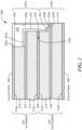
- First stripline board 202 includes a first conductor 222 and second stripline board 204 includes a second conductor 224, each of which may correspond to RF signal paths.
- An interconnect 220 couples the first conductor 222 to the second conductor 224.
- An electrically conductive wall (hereinafter 'conductive wall') 226 is formed over an outer surface 202c, 204c of first and second stripline boards 202, 204 to form a cavity 228 which encloses interconnect 220 and the outer surfaces 202c, 204c.
- conductive wall 226 may be formed on or otherwise disposed over at least one surface (e.g., edge, side, etc.) of multilayered PCB 200 such that it encloses interconnect 220 and the outer surfaces 202c, 204c.
- a first end 226a of conductive wall 226 may be coupled to first ground plane 206 and a second end 226b of conductive wall 226 may be coupled to second ground plane 208.
- Conductive wall 226 can be formed such that it encloses a spatial area around interconnect 220 and does not contact interconnect 220.
- Conductive wall 226 and cavity 228 can be formed using subtractive manufacturing techniques.
- the cavity 228 may be formed using subtractive manufacturing and conductive wall 226 can be printed over cavity 228.
- Cavity 228 may include or otherwise be filled a media that is substantially the same as the material from which dielectric substrates 210, 212, 214, 216 are provided from.
- the dimensions of the conductive wall 226 can be selected such that the dimensions are less than 0.1 of wavelengths in the cavity 228 inner (filled) media material.
- First end 226a is electrically coupled to a top surface of first ground plane 206 and second end 226a is electrically coupled to a surface of second dielectric substrate 216 or a bottom surface of second ground plane 208.
- Conductive wall 226 may be disposed such that it is flush or substantially flush with a top surface of first and second ground planes 206, 208.
- first end 226a may be coupled to an edge of first ground plane 206 such that it extends from the edge of first ground plane 206 and second end 226a may be coupled to an edge of second ground plane 208 such that it extends from the edge of second ground plane 208.
- first end 226a of conductive wall 226 may be coupled to first dielectric substrate 210 and second end 226b of conductive wall 226 may be coupled to second dielectric substrate 216.
- a ramp 234 may be formed over a portion of first surface 224a of second conductor 224 and aid interconnect 220 in coupling first and second conductors 222, 224.
- Ramp 234 can be disposed over the surface 224a of second conductor such that it facilitates the mechanical transition of the interconnect 220 from a vertical surface to horizontal surface 224a.
- ramp 234 may have a shape designed to generally guide interconnect 220 from the outer surface 202c of first stripline board 202 to first surface 224a of second conductor 224.
- ramp 234 has at least one of a ramp shape, triangle shape, wedge shape.
- a ramp 234 provided from a dielectric material may be provided on one end 230c of conductive layer 230 such that the dielectric material is disposed between the end 230c and interconnect 220.
- the ramp 234 (e.g., dielectric material) may insulate interconnect 220 from conductive layer 230.
- interconnect 220 is in contact with first and second conductors 222, 224 and not in contact with conductive layer 230.
- the electrically conductive wall 226 and cavity 228 can be configured to electrically isolate interconnect 220 from circuitry within multilayered PCB 200.
- cavity 228 may include or be filled with dielectric material.
- the dielectric material may be disposed between interconnect 220, outer surfaces 202c, 204c of the first and second stripline boards and an inner surface 226c of conductive wall 226.
- interconnect 220 may extend from a first end 222a of first conductor 222 to a first end 224a of second conductor 224.
- interconnect 220 (also referred to as a vertical RF interconnect) provides a signal path along which RF signals may be coupled from a first transmission line (i.e., first conductor 222) of first stripline board 202 to a second transmission line (i.e., conductor 224) of second stripline board 204.
- first transmission line i.e., first conductor 222
- second transmission line i.e., conductor 224
- vertical interconnect couples RF signals from one layer of multilayer circuit board 200 to a second, different layer of circuit board 200.
- first and second conductors 222, 224 respectively correspond to RF transmission lines, as well as center conductors of a stripline transmission line of first and second stripline boards 202, 204 respectively.
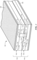
- a multilayered PCB 250 includes a conductor 280 disposed between first and second stripline boards 252, 254.
- First stripline board 252 provided from dielectric substrates 260, 262 having conductive ground planes 256, 280 disposed on outer surfaces 260a, 262b thereof.
- Second stripline board 254 is provided from dielectric substrates 264, 266 having conductive ground planes 280, 258 disposed on outer surfaces 264a, 266b thereof.
- conductive layer 280 is disposed between first and second stripline boards 252, 254 and serves as a ground plane for both stripline circuit boards 252, 254.
- First stripline board 252 includes a first conductor 272 and second stripline board 254 includes a second conductor 274, each of which may correspond to RF signal paths.
- An interconnect 270 couples the first conductor 272 to the second conductor 274.
- Multilayered PCB 250 may be substantially similar to multilayered PCB 200 of FIG. 2 , however at least one surface 250c (e.g., edge, side, etc.) of multilayered PCB 250 has a generally step shape.
- multilayered PCB 250 may include multiple dielectric substrates 260, 262, 264, 266 each having different dimensions (e.g., length, width).
- first stripline board 252 includes a first dielectric substrate 260 having a first length and a second dielectric substrate 262 having a second length.
- Second stripline board 254 includes a first dielectric substrate 264 having a third length and a fourth dielectric substrate 262 having a fourth length.
- One or more of dielectric substrates 260, 262, 264, 266 may have different lengths, thus one or more of the first, second, third and/or fourth lengths may be different.
- each of dielectric substrates 260, 262, 264, 266 have different lengths, thus each of the first, second, third and fourth lengths may be different to provide step shaped surface 250c.
- First conductor 272 may be formed or otherwise disposed over a first surface of second dielectric substrate 262 such that first conductor 272 has a length equal to the length of second dielectric substrate 262.
- Second conductor 274 may be formed or otherwise disposed over a first surface of second dielectric substrate 266 such that second conductor 274 has a length equal to the length of second dielectric substrate 266.
- Interconnect 270 may be formed on or otherwise disposed over the step shaped surface 250c of multilayered PCB 250 to couple first and second conductors 272, 274.
- One or more ramps 284a, 284b may be formed on different surfaces within multilayered PCB 250 to guide interconnect 270 along the step shaped surface from first conductor 272 to second conductor 274.
- a first ramp 284a may be formed on a first surface 280a of conductive layer 280 and a second ramp 284b may be formed on a first surface 274a of second conductor 274.
- FIG. 2A illustrates two ramps 284a, 284b formed within multilayered PCB 250
- any number of ramps may be formed within a multilayered PCB depending at least in part on the dimensions of the respective multilayered PCB and/or a number of steps formed by a surface of the respective multilayered PCB.
- Ramps 284a, 284b may include dielectric material. Ramps 284a, 284b may be formed in a variety of different shapes, including but not limited to, a triangle, a wedge, square, rectangle, etc. The shape of the ramps 284a, 284b may be based at least in part on the dimensions of the respective multilayered PCB and/or how an interconnect is coupled to a surface of the respective multilayered PCB.
- Conductive wall 276 may be formed over the outer surfaces 252c, 254c of first and second stripline boards 252, 254 respectively to form a cavity 278 which encloses interconnect 270 and outer surfaces 252c, 254c.
- a multilayered PCB 300 has portions thereof removed to reveal a first stripline board 302 and a second stripline board 304. It should be noted that for clarity in the figure and following description, certain dielectric layers and ground planes have been omitted from FIG. 3 .
- First and second stripline boards 302, 304 may include dielectric materials, such as but not limited to, Rogers 4003 laminates ® .
- First and second stripline boards 302, 304 can be bonded together by a bond film 330, such as but not limited to a conductive epoxy bond film or a pressure sensitive adhesive (PSA) film.
- a bond film 330 such as but not limited to a conductive epoxy bond film or a pressure sensitive adhesive (PSA) film.
- PSA pressure sensitive adhesive
- a first conductor 322 may be formed on or otherwise disposed over a first surface 302a of first stripline board 302 and a second conductor 324 may be formed on or otherwise disposed over a first surface 304a of second stripline board 304.
- First and second conductors 322, 324 may be formed
- first and second conductors 322, 324 may be printed onto first surface 302a of first stripline board 302 and first surface 304a of second stripline board 304, respectively.
- first and second conductors 322, 324 may include an ink stripline (e.g., Paru ink stripline) and can be printed through additive manufacturing techniques.
- First and second conductors may be electrically coupled together through an interconnect 320.
- Interconnect 320 may be formed on or otherwise disposed over an outer surface 302c of first stripline board 302. In some embodiments, interconnect 320 may be printed onto outer surface 302c of first stripline board 302 through techniques such as additive manufacturing.
- a ramp 334 may be formed over a portion of first surface 304a of second stripline board 304 to guide and aid interconnect 320 in coupling first and second conductors 322, 324.
- ramp 334 may be formed such that it is disposed over a bottom portion of outer surface 302c of first stripline board 302 and first surface 304a of second stripline board 304.
- Ramp 334 may have a shape designed to generally guide interconnect 320 from the outer surface 302c of first stripline board 302 to first surface 304a of second stripline board 304.
- ramp 334 has at least one of a ramp shape, triangle shape, wedge shape.
- ramp 334 may be printed onto the outer surface 302c of first stripline board 302 and/or first surface 304a of second stripline board 304.
- ramp 334 may include ink materials (e.g., creative materials inks) and can be printed through additive manufacturing techniques.
- a method 400 for forming a vertical interconnect on a multilayered PCB begins at block 402, by exposing a first signal path on a first layer of a stripline multilayer PCB.
- the first signal path in the first layer may be exposed to allow for a connection to be made to a different layer within the multilayered PCB.
- the stripline multilayer PCB may include multiple layers with each layer having stripline boards.
- a first stripline board (referred to herein as first stripline board, first layer or top stripline board) having a conductor (referred to herein as first conductor) may be provided as a first layer of the stripline multilayer PCB.
- the first stripline board (referred to herein as first stripline board or top stripline board) is formed on or otherwise disposed over a first surface of a conductive layer.
- the first stripline board may include multiple layers of dielectric material.
- the first stripline board may include first and second dielectric substrates. A second surface of the second dielectric substrate may be disposed on the first surface of the conductive layer.
- the conductive layer may be provided as a ground plane for the first stripline board.
- the first conductor is disposed between the dielectric layers.
- the first conductor may be formed over a first surface of the second dielectric substrate and under a second surface of a first dielectric substrate of the first stripline board.
- the first conductor can be formed as an RF signal path within first stripline board, such as a center conductor of a stripline transmission line.
- the conductor may be referred to herein as a first signal path.
- a portion of the dielectric material of the first stripline board may be removed.
- a portion of the first dielectric substrate may be removed to expose a portion of a first surface of the first signal path.
- the amount removed may vary, based at least in part on how an interconnect is coupled to the first signal path and how much surface area of first signal path is used to couple to the interconnect.
- the first stripline board may be formed such that the first signal path is exposed.
- the dielectric material may be provided below the first signal path, however, a portion of a top surface of the first signal path may not be covered by dielectric material and thus be exposed.
- a conductor may be disposed over a first surface of the first dielectric layer.
- the conductor may be provided as a ground plane and include any known conductive materials.
- a second signal path is exposed on a second different layer of the stripline multilayer printed circuit board.
- the second signal path corresponds to a second conductor within the multilayered PCB.
- a second stripline board (referred to herein as second stripline board or bottom stripline board) having a conductor (referred to herein as second conductor) may be provided as a second layer of the stripline multilayer PCB.
- the second stripline board may include dielectric layers and the second conductor may be disposed between the dielectric layers.
- the second conductor can be disposed over a first surface of a second dielectric substrate with the second dielectric substrate serving as a base or bottom portion for the second stripline board.
- a first dielectric substrate can be disposed over a first surface of the second conductor with the first dielectric substrate serving as a top portion of the second stripline board.
- the second conductor can be formed as an RF signal path within second stripline board, such as a center conductor of a stripline transmission line.
- a portion of the dielectric material of the second stripline board may be removed to expose a portion of the second signal path.
- a portion of the first dielectric substrate may be removed to expose a portion of a first surface of the second signal path.
- the amount removed may vary, based at least in part on how the interconnect is coupled to the second signal path and how much surface area of second signal path is used to couple to the interconnect.
- the second stripline board may be formed such that the second signal path is exposed.
- the dielectric material may be provided below the second signal path, however, a portion of a top surface of the second signal path may not be covered by dielectric material and thus be exposed.
- a conductor may be disposed over a second surface of the second dielectric layer.
- the conductor may be provided as a ground plane and include any known conductive materials.
- the conductive layer can be formed on or otherwise disposed over a first surface of the second stripline board.
- the conductive layer may be provided as a ground plane for the second stripline board.
- the conductive layer may be formed such that it separates different layers within the multilayered PCB (i.e., between a first and second stripline board).
- a bonding layer may be disposed between first and second stripline boards.
- the conductive layer may be provided as part of a dielectric substrate in the first and/or second stripline board and a bond film or other bond material may be disposed between the conductive layer and the surface of dielectric substrates of first and/or second stripline boards.
- the layers and thus the stripline boards may be formed having equal dimensions (e.g., length, height, width).
- the first and second stripline boards may be formed such they have equal lengths and the outer surfaces (e.g., a side portion, an edge) of the first and second stripline boards are substantially flush.
- the dielectric layers of the first and second stripline boards may be formed having equal dimensions.
- the first and second dielectric substrates of the first stripline board and the first and second dielectric substrates of the second stripline board may have equal dimensions such that ends or side portions of the dielectric substrates are substantially flush.
- the layers and thus the stripline boards may be formed having different dimensions (e.g., length, height, width).
- the first and second stripline boards may be formed such they have different lengths and the outer surfaces of the first and second stripline boards form a step shaped surface.
- the dielectric layers may be formed having different dimensions.
- one or more of the first and second dielectric substrates of the first stripline board and the first and second dielectric substrates of the second stripline board may have different dimensions such that ends or side portions of the dielectric substrates form a step shape.
- each of the dielectric substrates have different dimensions.
- the first stripline board and the second stripline board may serve as common building blocks for the multilayered PCB.
- the first and second stripline boards can be fabricated from virtually any PTFE based material having the desired microwave properties.
- the individual stripline boards within the multilayered PCB can be fabricated with material reinforced with woven glass cloth.
- the first and second stripline boards can be fabricated separately and then coupled via the conductive layer to provide the multilayered PCB.
- the conductive layer can correspond to a bonding layer.
- the conductive layer may include Cyanate Ester resin B-stage (e.g. the type manufactured by W. L. Gore & Associates and sold under the trade name Speedboard-C ® ).
- the first and second stripline boards can be bonded or otherwise secured together to provide the multilayered PCB.
- the multilayered PCB may be provided as a bonded assembly.
- the multilayered PCB can be the result of multiple lamination, bonding and assembly processes.
- each subassembly e.g., individual stripline boards
- any subassembly which does not meet or exceed desired electrical and/or mechanical performance characteristics may be identified and either repaired or not used to form multilayered PCB
- separate fabrication of the individual stripline boards allows the fabrication process for each stripline board to be separately optimized for maximum yield of that respective stripline board
- separate fabrication of stripline boards which are then secured together via bonding layers results in a wider choice of bonding adhesives and bonding temperatures for each stripline board, which leads to improved mechanical performance for each stripline board.
- the fabrication and assembly approach developed for the multilayered PCB produces a robust mechanical design that significantly improves manufacturing yield.
- each circuit layer of the multilayered PCB can be fabricated using PCB industry standard processes and fabrication tolerances and commercially available materials.
- a ramp may be formed over a portion of the second signal path.
- one or more ramps may be formed on different layers of the multilayered PCB to facilitate the transition of an interconnect from different surfaces of the different layers, for example, from a substantially vertical surface to a substantially horizontal surface.
- the different layers of the multilayered PCB may form a step shaped surface along a side portion or edge of the multilayered PCB.
- One or more ramps may be disposed on one or more surfaces of the dielectric substrates to guide the interconnect along the step shaped surface.
- the ramps may be provided to provide a ramp like structure for the interconnect to flow from one layer to a next, different layer, such as from one dielectric substrate to another dielectric substrate, or from one conductor to a second different conductor within the multilayered PCB.
- the ramps may be formed from and include dielectric material.
- the ramps may be formed in a variety of different shapes, for example, the shape of a particular ramp may be based at least in part on the dimensions of the different dielectric substrates within the multilayered PCB. Further, one ramp or multiple ramps may be formed in a multilayered PCB based at least in part on a number of steps formed and/or the dimensions of the different dielectric substrates within the multilayered PCB.
- dielectric material may be provided on one end or side of the conductive layer disposed between the first and second stripline boards to insulate the interconnect from the conductive layer as the interconnect extends along the outer surfaces of the first and second stripline boards.
- the dielectric material may be disposed between the interconnect and the conductive layer such that the interconnect does not contact the conductive layer between the first and second stripline boards.
- the ramp can be optional and thus, in some embodiments, a ramp is not used and the multilayered PCB may not include a ramp.
- the vertical interconnect can be formed along portions of an outer surface of the first and second layers to electrically couple the first and second signal paths.
- the vertical interconnect can be disposed on or otherwise formed on outer surfaces, such as an edge or side portion, of the dielectric layers of the first and second stripline boards.
- the interconnect can extend from the first conductor, along a side portion of the second dielectric substrate of the first stripline board and a side portion of the first dielectric substrate of the second stripline board to the second conductor.
- the shape or configuration of the interconnect may depend at least in part on the shape of the outer surface of the different layers of the multilayered PCB.
- the shape of the interconnect may include, but not be limited to, a cylindrical shape, part cylindrical shape, rectangular shape, part rectangular shape, a shape that is conformal to a surface of the first and second dielectric stripline boards (e.g., conformal to a side portion, edge) or any combination of these.
- the interconnect may be provided in a generally vertical direction along the outer surfaces.
- the interconnect may be positioned such that it is perpendicular to the outer surfaces of each of the first and second stripline boards.
- the interconnect may be formed over or otherwise disposed on the step shaped surface.
- the interconnect may be formed such that its respective shape includes multiple orientations (e.g., substantially vertical portions, substantially horizontal portions, portions at or near an angle ranging from about 0° to about 90°, etc.).
- the vertical interconnect may be a conductor provided from any suitable conductive material or otherwise disposed on surfaces of the dielectric substrates.
- the vertical interconnect may be printed onto a surface of one or more dielectric substrates using additive manufacturing techniques.
- the vertical interconnect may include various types of conductive inks.
- an electrically conductive wall is formed over the side portions of the first and second layers to form a cavity which encloses the vertical interconnect and the side portions of the first and second layers.
- the conductive wall can be formed or otherwise disposed over an edge or side of the multilayered PCB such that it encloses one side or edge of each of the first and second stripline boards.
- a first end of the conductive wall can be coupled to the first (or top) ground plane disposed over the first surface of the first stripline board and a second end of the conductive wall can be coupled to the second (or bottom) ground plane disposed over (or under) the second surface of the second stripline board.
- the conductive wall can extend an entire height (or length) of one side of the multilayered PCB, from the top ground plane to the bottom ground plane.
- the first end of the conductive wall may be coupled to a top surface of first ground plane and second end may be coupled to a bottom surface of second ground plane.
- the first end may be coupled to an edge of first ground plane such that it extends from the edge of first ground plane and second end may be coupled to an edge of second ground plane such that it extends from the edge of second ground plane.
- the conductive wall may be coupled such that it is flush or substantially flush with a top surface of first and a bottom surface of second ground plane.
- the conductive wall can be formed such that it encloses a spatial area around the interconnect and does not contact the interconnect.
- the conductive wall and resulting cavity can be formed using subtractive manufacturing techniques.
- the cavity may be formed using subtractive manufacturing and the conductive wall can be printed over the material making up the cavity.
- the cavity may include or otherwise be filled a media that is substantially the same as the material from which the dielectric substrates are provided from.
- a cut-out may be formed on an edge or side portion of the conductive layer to ensure that the interconnect does not contact the conductive layer.
- a portion of the interconnect may pass by an edge or side portion of the conductive layer.
- the cut-out may be formed along the edge or side portion such that it is adjacent to the portion of the interconnect that passes by the edge or side portion.
- the dimensions (e.g., width, length) of the cut-out can correspond to the dimensions (e.g., width, length) and be selected such that the interconnect does not contact the conductive layer.
- the cut-out may be filled with dielectric material and the interconnect may be formed on or otherwise disposed over the dielectric material within the cut-out.
- the conductive wall may be formed such that it resides within an assembly that houses a multilayered PCB or within the multilayered PCB itself.
- the conductive wall may be formed such that it resides within the multilayered PCB assembly and is surrounded by dielectric material that forms an outer surface or edge of the multilayered PCB.
- the conductive wall does not form an edge or outer surface of the multilayered PCB.
- the conductive wall may be formed to protect and/or insulate the interconnect and thus may be formed in a variety of different shapes or designs based at least in part on the location and/or dimensions of the interconnect.
- the conductive wall may insulate the interconnect from surrounding circuitry in the multilayered PCB, thereby preventing signals from "leaking" between signals paths.
- the conductive wall may be formed having, but not limited to, a cylindrical shape, part cylindrical shape, rectangular shape, part rectangular shape, a shape that is conformal to a surface of the multilayered printed circuit board (e.g., conformal to a side portion) or any combination of these.
- the first end of the conductive wall may be coupled to the top ground plane, the first dielectric substrate of the first stripline board, the second dielectric substrate of the first stripline board or a combination of them.
- the second end of the conductive wall may be coupled to the bottom ground plane, the first dielectric substrate of the second stripline board, the second dielectric substrate of the second stripline board or a combination of them.
- the first end of the conductive wall may be coupled to the first dielectric substrate of the first stripline board and the second end of the conductive wall may be coupled to the second dielectric substrate of the second stripline board. In other embodiments, the first end of the conductive wall may be coupled to the top ground plane and the second end of the conductive wall may be coupled to the second dielectric substrate of the second stripline board.
- the conductive wall may include conductive materials, such as various metals or printed metals.
- the conductive wall forms a cavity which encloses the interconnect and outer surfaces of the first and second stripline boards.
- the cavity may include or be filled with dielectric material.
- dielectric material may be disposed between the interconnect, outer surfaces of the first and second stripline boards and an inner surface of the conductive wall.
- the first stripline board and the second stripline board can be formed having different lengths such that the outer surface of the second dielectric substrate of the first stripline and the outer surface of the first dielectric substrate of the second stripline form a step shaped surface.
- a multilayered PCB having a first and second stripline board the systems and methods as described herein are not limited to a multilayered PCB having only two stripline boards.
- a multilayered PCB may be fabricated having any number of stripline boards (e.g., more than two) using the systems and methods described herein, based at least in part on a particular application of the multilayered PCB.
Landscapes
- Engineering & Computer Science (AREA)
- Microelectronics & Electronic Packaging (AREA)
- Manufacturing & Machinery (AREA)
- Physics & Mathematics (AREA)
- Electromagnetism (AREA)
- Structure Of Printed Boards (AREA)
- Production Of Multi-Layered Print Wiring Board (AREA)
- Waveguide Connection Structure (AREA)
- Waveguides (AREA)
Claims (15)
- Mehrlagige Leiterplatte (200), umfassend:eine erste Streifenleiterplatte (202), die eine erste und eine zweite gegenüberliegende Oberfläche aufweist, wobei die erste Streifenleiterplatte einen ersten Leiter (222) aufweist, der als ein erster Signalweg innerhalb der mehrlagigen Leiterplatte ausgebildet ist;eine zweite Streifenleiterplatte (204), die eine erste und eine zweite gegenüberliegende Oberfläche aufweist, wobei die zweite Streifenleiterplatte einen zweiten Leiter (224) aufweist, der als ein zweiter Signalweg innerhalb der mehrlagigen Leiterplatte ausgebildet ist;eine vertikale Verbindung (220), die entlang von Abschnitten einer Außenoberfläche (202c, 204c) der ersten und der zweiten Streifenleiterplatte angeordnet ist, wobei die vertikale Verbindung ein erstes Ende aufweist, das elektrisch mit dem ersten Leiter gekoppelt ist, und ein zweites Ende, das elektrisch mit dem zweiten Leiter gekoppelt ist, wobei die Außenoberfläche der ersten und der zweiten Streifenleiterplatte einen Seitenabschnitt der ersten Streifenleiterplatte und der zweiten Streifenleiterplatte umfasst;eine elektrisch leitende Wand (226c), die über der Außenoberfläche der ersten und der zweiten Streifenleiterplatte ausgebildet ist, um einen Hohlraum (228) zu bilden, wobei die elektrisch leitende Wand (226c) die vertikale Verbindung und die Außenoberfläche der ersten und der zweiten Streifenleiterplatte umschließt, wobei die elektrisch leitende Wand die Außenoberfläche so umschließt, dass der Hohlraum zwischen der Außenoberfläche der ersten und der zweiten Streifenleiterplatte und einer Innenoberfläche (226c) der elektrisch leitenden Wand gebildet wird;eine leitende Schicht (230), wobei die leitende Schicht zwischen der ersten Streifenleiterplatte und der zweiten Streifenleiterplatte angeordnet ist und als Massefläche für die erste Streifenleiterplatte und die zweite Streifenleiterplatte dient; undeine Rampe (234), die aus einem dielektrischen Material bereitgestellt wird, das an einem Ende (230c) der leitenden Schicht bereitgestellt wird, sodass das dielektrische Material zwischen dem Ende und der vertikalen Verbindung angeordnet ist,wobei die Rampe konfiguriert ist, um die vertikale Verbindung von der leitenden Schicht zu isolieren.
- Mehrlagige Leiterplatte nach Anspruch 1, wobei die erste Streifenleiterplatte ferner Folgendes umfasst:ein erstes dielektrisches Substrat, das über einer ersten Oberfläche des ersten Leiters angeordnet ist, und ein zweites dielektrisches Substrat, das über einer zweiten Oberfläche des ersten Leiters angeordnet ist; undeine erste Massefläche, die über einer ersten Oberfläche des ersten dielektrischen Substrats gebildet ist.
- Mehrlagige Leiterplatte nach Anspruch 2, wobei die leitende Schicht über einer zweiten Oberfläche des zweiten dielektrischen Substrats ausgebildet ist, um eine zweite Massefläche der ersten Streifenleiterplatte zu bilden.
- Mehrlagige Leiterplatte nach Anspruch 1, wobei die zweite Streifenleiterplatte ferner Folgendes umfasst:ein erstes dielektrisches Substrat, das über einer ersten Oberfläche des zweiten Leiters angeordnet ist, und ein zweites dielektrisches Substrat, das über einer zweiten Oberfläche des zweiten Leiters angeordnet ist; undeine erste Massefläche, die über einer zweiten Oberfläche des zweiten dielektrischen Substrats gebildet ist.
- Mehrlagige Leiterplatte nach Anspruch 4, wobei die leitende Schicht über einer ersten Oberfläche des ersten dielektrischen Substrats ausgebildet ist, um eine zweite Massefläche der zweiten Streifenleiterplatte zu bilden.
- Mehrlagige Leiterplatte nach Anspruch 1, wobei die vertikale Verbindung entlang einer Außenoberfläche eines zweiten dielektrischen Substrats der ersten Streifenleiterplatte und einer Außenoberfläche eines ersten dielektrischen Substrats der zweiten Streifenleiterplatte ausgebildet ist.
- Mehrlagige Leiterplatte nach Anspruch 6, wobei:die Außenoberfläche des zweiten dielektrischen Substrats der ersten Streifenleiterplatte und die Außenoberfläche des ersten dielektrischen Substrats der zweiten Streifenleiterplatte im Wesentlichen bündig sind; oderdie erste Streifenleiterplatte und die zweite Streifenleiterplatte unterschiedlich lang sind, sodass die Außenoberfläche des zweiten dielektrischen Substrats der ersten Streifenleiterplatte und die Außenoberfläche des ersten dielektrischen Substrats der zweiten Streifenleiterplatte eine stufenförmige Oberfläche bilden.
- Mehrlagige Leiterplatte nach Anspruch 1, wobei die vertikale Verbindung über der Rampe angeordnet ist, um die ersten und zweiten Leiter über eine stufenförmige Oberfläche zu koppeln, die von den Außenoberflächen der ersten und zweiten Streifenleiterplatten gebildet wird.
- Mehrlagige Leiterplatte nach Anspruch 1,wobei die elektrisch leitende Wand mit der ersten Oberfläche der ersten Streifenleiterplatte und der zweiten Oberfläche der zweiten Streifenleiterplatte gekoppelt ist; oderferner umfassend dielektrisches Material, das in dem Hohlraum angeordnet ist; oderwobei eine Form der Verbindung mindestens eine von einer zylindrischen Form, einer rechteckigen Form oder eine an die Außenoberfläche der ersten und zweiten Streifenleiterplatte angepasste Form beinhaltet; oderwobei eine Form der elektrisch leitfähigen Wand mindestens eine von einer zylindrischen Form, einer rechteckigen Form oder eine an eine Oberfläche der mehrlagigen Leiterplatte angepasste Form beinhaltet.
- Verfahren (400) zum Herstellen einer mehrlagigen Leiterplatte, wobei das Verfahren folgendes umfasst:Freilegen (402) eines ersten Signalwegs auf einer ersten Schicht einer mehrlagigen Streifenleitungs-Leiterplatte;Freilegen (404) eines zweiten Signalwegs auf einer zweiten unterschiedlichen Schicht der mehrlagigen Streifenleitungs-Leiterplatte;Bereitstellen (408) einer vertikalen Verbindung auf Seitenabschnitten der ersten und zweiten Schicht der mehrlagigen Streifenleitungs-Leiterplatte; undBilden (410) einer elektrisch leitenden Wand über den Seitenabschnitten der ersten und zweiten Schicht der mehrlagigen Streifenleitungs-Leiterplatte, um einen Hohlraum zu bilden, wobei der Hohlraum die vertikale Verbindung und die Seitenabschnitte der ersten und zweiten Schicht umschließt,wobei die elektrisch leitende Wand die Seitenabschnitte so umschließt, dass der Hohlraum zwischen den Seitenabschnitten der ersten und zweiten Schicht und einer inneren Oberfläche der elektrisch leitenden Wand gebildet wird;wobei die mehrlagige Leiterplatte eine leitende Schicht (230) umfasst, wobei die leitende Schicht zwischen der ersten und zweiten Schicht angeordnet ist und als Massefläche für die erste und zweite Schicht dient; undwobei die mehrlagige Leiterplatte eine Rampe (234) umfasst, die aus einem dielektrischen Material bereitgestellt wird, das an einem Ende (230c) der leitenden Schicht bereitgestellt wird, sodass das dielektrische Material zwischen dem Ende und der vertikalen Verbindung angeordnet ist, wobei die Rampe konfiguriert ist, um die vertikale Verbindung von der leitenden Schicht zu isolieren.
- Verfahren nach Anspruch 10, wobei Bilden der ersten Schicht ferner Folgendes umfasst:Anordnen eines ersten dielektrischen Substrats über einer ersten Oberfläche des ersten Signalwegs und eines zweiten dielektrischen Substrats über einer zweiten Oberfläche des ersten Signalwegs; undBilden einer ersten Massefläche über einer ersten Oberfläche des ersten dielektrischen Substrats.
- Verfahren nach Anspruch 11, ferner umfassend Bilden der leitfähigen Schicht über einer zweiten Oberfläche des zweiten dielektrischen Substrats.
- Verfahren nach Anspruch 10, wobei Bilden der zweiten Schicht ferner Folgendes umfasst:Anordnen eines ersten dielektrischen Substrats über einer ersten Oberfläche des zweiten Signalwegs und eines zweiten dielektrischen Substrats über einer zweiten Oberfläche des zweiten Signalwegs; undBilden einer ersten Massefläche über einer zweiten Oberfläche des zweiten dielektrischen Substrats; und optional ferner umfassend Bilden der leitfähigen Schicht über einer ersten Oberfläche des ersten dielektrischen Substrats.
- Verfahren nach Anspruch 10, ferner umfassend Anordnen der vertikalen Verbindung entlang einer Außenoberfläche eines zweiten dielektrischen Substrats der ersten Schicht und einer Außenoberfläche eines ersten dielektrischen Substrats der zweiten Schicht; und optional
Bereitstellen der ersten Schicht und der zweiten Schicht der mehrlagigen Leiterplatte mit unterschiedlichen Längen, sodass die Außenoberfläche des zweiten dielektrischen Substrats der ersten Schicht und die Außenoberfläche des ersten dielektrischen Substrats der zweiten Schicht eine stufenförmige Oberfläche bilden; und optional ferner umfassend:
Bilden einer zweiten Rampe über einen Abschnitt des zweiten Signalwegs, wobei die vertikale Verbindung über Abschnitte der Rampe und der zweiten Rampe gebildet wird. - Verfahren nach Anspruch 10, ferner umfassend:Koppeln der elektrisch leitenden Wand mit einer ersten Oberfläche der ersten Schicht und einer zweiten Oberfläche der zweiten Schicht; oderAnordnen von dielektrischem Material innerhalb des Hohlraums.
Applications Claiming Priority (2)
| Application Number | Priority Date | Filing Date | Title |
|---|---|---|---|
| US15/392,142 US9974160B1 (en) | 2016-12-28 | 2016-12-28 | Interconnection system for a multilayered radio frequency circuit and method of fabrication |
| PCT/US2017/068075 WO2018125775A1 (en) | 2016-12-28 | 2017-12-22 | An interconnection system for a multilayered radio frequency circuit and method of fabrication |
Publications (2)
| Publication Number | Publication Date |
|---|---|
| EP3563447A1 EP3563447A1 (de) | 2019-11-06 |
| EP3563447B1 true EP3563447B1 (de) | 2024-08-21 |
Family
ID=60991633
Family Applications (1)
| Application Number | Title | Priority Date | Filing Date |
|---|---|---|---|
| EP17829883.2A Active EP3563447B1 (de) | 2016-12-28 | 2017-12-22 | Verbindungssystem für eine mehrlagige hochfrequenzschaltung und verfahren zur herstellung |
Country Status (6)
| Country | Link |
|---|---|
| US (1) | US9974160B1 (de) |
| EP (1) | EP3563447B1 (de) |
| JP (1) | JP6664769B2 (de) |
| KR (1) | KR102315533B1 (de) |
| CN (1) | CN110140255B (de) |
| WO (1) | WO2018125775A1 (de) |
Families Citing this family (6)
| Publication number | Priority date | Publication date | Assignee | Title |
|---|---|---|---|---|
| TWI696197B (zh) * | 2018-11-21 | 2020-06-11 | 貿聯國際股份有限公司 | 高頻軟性扁平排線 |
| WO2022067569A1 (zh) * | 2020-09-29 | 2022-04-07 | 华为技术有限公司 | 信号传输装置及电子设备 |
| CN113035845B (zh) * | 2021-02-05 | 2022-07-12 | 珠海越亚半导体股份有限公司 | 具有天线的封装结构及其制作方法 |
| CN115226297B (zh) * | 2021-04-21 | 2026-02-17 | 宏启胜精密电子(秦皇岛)有限公司 | 多层线路板及其制备方法 |
| US12564064B2 (en) | 2023-01-12 | 2026-02-24 | Bae Systems Information And Electronic Systems Integration Inc. | RF bridge |
| CN119277640B (zh) * | 2024-12-09 | 2025-03-04 | 沈阳航盛科技有限责任公司 | 一种抗信号干扰的印刷电路板 |
Family Cites Families (13)
| Publication number | Priority date | Publication date | Assignee | Title |
|---|---|---|---|---|
| JPH0429205U (de) * | 1990-07-02 | 1992-03-09 | ||
| US5657537A (en) | 1995-05-30 | 1997-08-19 | General Electric Company | Method for fabricating a stack of two dimensional circuit modules |
| JPH11308021A (ja) * | 1998-04-23 | 1999-11-05 | Nec Corp | 高周波パッケージの接続構造 |
| JP3976473B2 (ja) * | 2000-05-09 | 2007-09-19 | 日本電気株式会社 | 高周波回路及びそれを用いたモジュール、通信機 |
| US6933450B2 (en) | 2002-06-27 | 2005-08-23 | Kyocera Corporation | High-frequency signal transmitting device |
| TWI335101B (en) * | 2007-06-27 | 2010-12-21 | Ind Tech Res Inst | Vertical coupling structure for non-adjacent resonators |
| US20090008139A1 (en) * | 2007-07-03 | 2009-01-08 | Sony Ericsson Mobile Communications Ab | Multilayer pwb and a method for producing the multilayer pwb |
| US7880570B2 (en) * | 2007-10-25 | 2011-02-01 | Finisar Corporation | Feed thru with flipped signal plane using guided vias |
| JP4656212B2 (ja) * | 2008-06-13 | 2011-03-23 | ソニー株式会社 | 接続方法 |
| WO2013008292A1 (ja) * | 2011-07-11 | 2013-01-17 | 株式会社日立製作所 | 電磁波伝搬路および電磁波伝搬装置 |
| CN104364897B (zh) * | 2012-10-29 | 2017-07-25 | 京瓷株式会社 | 元件收纳用封装件以及安装结构体 |
| CN105633525A (zh) * | 2015-12-28 | 2016-06-01 | 青岛玻莱莫斯新材料技术有限公司 | 一种多层巴伦 |
| CN105846032B (zh) * | 2016-03-24 | 2018-04-27 | 中国计量学院 | 一种低损耗交叉叠层式ltcc威尔金森功分器 |
-
2016
- 2016-12-28 US US15/392,142 patent/US9974160B1/en active Active
-
2017
- 2017-12-22 WO PCT/US2017/068075 patent/WO2018125775A1/en not_active Ceased
- 2017-12-22 JP JP2019535230A patent/JP6664769B2/ja active Active
- 2017-12-22 CN CN201780081380.8A patent/CN110140255B/zh active Active
- 2017-12-22 KR KR1020197020428A patent/KR102315533B1/ko active Active
- 2017-12-22 EP EP17829883.2A patent/EP3563447B1/de active Active
Also Published As
| Publication number | Publication date |
|---|---|
| CN110140255B (zh) | 2021-08-24 |
| CN110140255A (zh) | 2019-08-16 |
| EP3563447A1 (de) | 2019-11-06 |
| WO2018125775A1 (en) | 2018-07-05 |
| JP2020503685A (ja) | 2020-01-30 |
| KR102315533B1 (ko) | 2021-10-20 |
| JP6664769B2 (ja) | 2020-03-13 |
| KR20190094423A (ko) | 2019-08-13 |
| US9974160B1 (en) | 2018-05-15 |
Similar Documents
| Publication | Publication Date | Title |
|---|---|---|
| EP3563447B1 (de) | Verbindungssystem für eine mehrlagige hochfrequenzschaltung und verfahren zur herstellung | |
| CN109004375B (zh) | 天线集成印刷线路板及其制造方法 | |
| US11375609B2 (en) | Method of manufacturing radio frequency interconnections | |
| US11133594B2 (en) | System and method with multilayer laminated waveguide antenna | |
| US5382931A (en) | Waveguide filters having a layered dielectric structure | |
| CA2663800C (en) | Tile sub-array and phase array antenna circuits and techniques | |
| US6356245B2 (en) | Microwave strip transmission lines, beamforming networks and antennas and methods for preparing the same | |
| EP2449621B1 (de) | Geneigte hybridantenne mit einer einzigen apertur | |
| EP3847722B1 (de) | Rf schaltkreismodul umfassend einer leiterplatte | |
| US20060017529A1 (en) | Multi-layer integrated RF/IF circuit board | |
| JP7544335B2 (ja) | アンテナ・モジュール、アンテナ・モジュールの製造方法、及び電子デバイス | |
| US20060019505A1 (en) | Multi-layer integrated RF/IF circuit board | |
| KR102459055B1 (ko) | 개선 통신 어레이 | |
| US11069980B2 (en) | Layered waveguide system and method of forming a waveguide | |
| CN107926112A (zh) | 电路结构 | |
| EP4473618A1 (de) | Gruppenantenne gebildet durch subarray-antennen |
Legal Events
| Date | Code | Title | Description |
|---|---|---|---|
| STAA | Information on the status of an ep patent application or granted ep patent |
Free format text: STATUS: UNKNOWN |
|
| STAA | Information on the status of an ep patent application or granted ep patent |
Free format text: STATUS: THE INTERNATIONAL PUBLICATION HAS BEEN MADE |
|
| PUAI | Public reference made under article 153(3) epc to a published international application that has entered the european phase |
Free format text: ORIGINAL CODE: 0009012 |
|
| STAA | Information on the status of an ep patent application or granted ep patent |
Free format text: STATUS: REQUEST FOR EXAMINATION WAS MADE |
|
| 17P | Request for examination filed |
Effective date: 20190712 |
|
| AK | Designated contracting states |
Kind code of ref document: A1 Designated state(s): AL AT BE BG CH CY CZ DE DK EE ES FI FR GB GR HR HU IE IS IT LI LT LU LV MC MK MT NL NO PL PT RO RS SE SI SK SM TR |
|
| AX | Request for extension of the european patent |
Extension state: BA ME |
|
| DAV | Request for validation of the european patent (deleted) | ||
| DAX | Request for extension of the european patent (deleted) | ||
| STAA | Information on the status of an ep patent application or granted ep patent |
Free format text: STATUS: EXAMINATION IS IN PROGRESS |
|
| 17Q | First examination report despatched |
Effective date: 20210111 |
|
| GRAP | Despatch of communication of intention to grant a patent |
Free format text: ORIGINAL CODE: EPIDOSNIGR1 |
|
| STAA | Information on the status of an ep patent application or granted ep patent |
Free format text: STATUS: GRANT OF PATENT IS INTENDED |
|
| RIC1 | Information provided on ipc code assigned before grant |
Ipc: H05K 3/46 20060101ALN20240202BHEP Ipc: H05K 1/14 20060101ALN20240202BHEP Ipc: H05K 1/02 20060101ALI20240202BHEP Ipc: H05K 3/40 20060101ALI20240202BHEP Ipc: H01P 5/02 20060101AFI20240202BHEP |
|
| GRAJ | Information related to disapproval of communication of intention to grant by the applicant or resumption of examination proceedings by the epo deleted |
Free format text: ORIGINAL CODE: EPIDOSDIGR1 |
|
| INTG | Intention to grant announced |
Effective date: 20240222 |
|
| STAA | Information on the status of an ep patent application or granted ep patent |
Free format text: STATUS: EXAMINATION IS IN PROGRESS |
|
| GRAP | Despatch of communication of intention to grant a patent |
Free format text: ORIGINAL CODE: EPIDOSNIGR1 |
|
| STAA | Information on the status of an ep patent application or granted ep patent |
Free format text: STATUS: GRANT OF PATENT IS INTENDED |
|
| INTC | Intention to grant announced (deleted) | ||
| RIC1 | Information provided on ipc code assigned before grant |
Ipc: H05K 3/46 20060101ALN20240327BHEP Ipc: H05K 1/14 20060101ALN20240327BHEP Ipc: H05K 1/02 20060101ALI20240327BHEP Ipc: H05K 3/40 20060101ALI20240327BHEP Ipc: H01P 5/02 20060101AFI20240327BHEP |
|
| INTG | Intention to grant announced |
Effective date: 20240412 |
|
| GRAS | Grant fee paid |
Free format text: ORIGINAL CODE: EPIDOSNIGR3 |
|
| GRAA | (expected) grant |
Free format text: ORIGINAL CODE: 0009210 |
|
| STAA | Information on the status of an ep patent application or granted ep patent |
Free format text: STATUS: THE PATENT HAS BEEN GRANTED |
|
| AK | Designated contracting states |
Kind code of ref document: B1 Designated state(s): AL AT BE BG CH CY CZ DE DK EE ES FI FR GB GR HR HU IE IS IT LI LT LU LV MC MK MT NL NO PL PT RO RS SE SI SK SM TR |
|
| REG | Reference to a national code |
Ref country code: GB Ref legal event code: FG4D |
|
| REG | Reference to a national code |
Ref country code: CH Ref legal event code: EP |
|
| REG | Reference to a national code |
Ref country code: DE Ref legal event code: R096 Ref document number: 602017084301 Country of ref document: DE |
|
| REG | Reference to a national code |
Ref country code: IE Ref legal event code: FG4D |
|
| REG | Reference to a national code |
Ref country code: LT Ref legal event code: MG9D |
|
| REG | Reference to a national code |
Ref country code: NL Ref legal event code: MP Effective date: 20240821 |
|
| REG | Reference to a national code |
Ref country code: AT Ref legal event code: MK05 Ref document number: 1716448 Country of ref document: AT Kind code of ref document: T Effective date: 20240821 |
|
| PG25 | Lapsed in a contracting state [announced via postgrant information from national office to epo] |
Ref country code: PL Free format text: LAPSE BECAUSE OF FAILURE TO SUBMIT A TRANSLATION OF THE DESCRIPTION OR TO PAY THE FEE WITHIN THE PRESCRIBED TIME-LIMIT Effective date: 20240821 Ref country code: PT Free format text: LAPSE BECAUSE OF FAILURE TO SUBMIT A TRANSLATION OF THE DESCRIPTION OR TO PAY THE FEE WITHIN THE PRESCRIBED TIME-LIMIT Effective date: 20241223 Ref country code: NL Free format text: LAPSE BECAUSE OF FAILURE TO SUBMIT A TRANSLATION OF THE DESCRIPTION OR TO PAY THE FEE WITHIN THE PRESCRIBED TIME-LIMIT Effective date: 20240821 Ref country code: GR Free format text: LAPSE BECAUSE OF FAILURE TO SUBMIT A TRANSLATION OF THE DESCRIPTION OR TO PAY THE FEE WITHIN THE PRESCRIBED TIME-LIMIT Effective date: 20241122 Ref country code: FI Free format text: LAPSE BECAUSE OF FAILURE TO SUBMIT A TRANSLATION OF THE DESCRIPTION OR TO PAY THE FEE WITHIN THE PRESCRIBED TIME-LIMIT Effective date: 20240821 |
|
| PG25 | Lapsed in a contracting state [announced via postgrant information from national office to epo] |
Ref country code: BG Free format text: LAPSE BECAUSE OF FAILURE TO SUBMIT A TRANSLATION OF THE DESCRIPTION OR TO PAY THE FEE WITHIN THE PRESCRIBED TIME-LIMIT Effective date: 20240821 |
|
| PG25 | Lapsed in a contracting state [announced via postgrant information from national office to epo] |
Ref country code: LV Free format text: LAPSE BECAUSE OF FAILURE TO SUBMIT A TRANSLATION OF THE DESCRIPTION OR TO PAY THE FEE WITHIN THE PRESCRIBED TIME-LIMIT Effective date: 20240821 |
|
| PG25 | Lapsed in a contracting state [announced via postgrant information from national office to epo] |
Ref country code: IS Free format text: LAPSE BECAUSE OF FAILURE TO SUBMIT A TRANSLATION OF THE DESCRIPTION OR TO PAY THE FEE WITHIN THE PRESCRIBED TIME-LIMIT Effective date: 20241221 Ref country code: AT Free format text: LAPSE BECAUSE OF FAILURE TO SUBMIT A TRANSLATION OF THE DESCRIPTION OR TO PAY THE FEE WITHIN THE PRESCRIBED TIME-LIMIT Effective date: 20240821 |
|
| PG25 | Lapsed in a contracting state [announced via postgrant information from national office to epo] |
Ref country code: HR Free format text: LAPSE BECAUSE OF FAILURE TO SUBMIT A TRANSLATION OF THE DESCRIPTION OR TO PAY THE FEE WITHIN THE PRESCRIBED TIME-LIMIT Effective date: 20240821 |
|
| PG25 | Lapsed in a contracting state [announced via postgrant information from national office to epo] |
Ref country code: ES Free format text: LAPSE BECAUSE OF FAILURE TO SUBMIT A TRANSLATION OF THE DESCRIPTION OR TO PAY THE FEE WITHIN THE PRESCRIBED TIME-LIMIT Effective date: 20240821 Ref country code: RS Free format text: LAPSE BECAUSE OF FAILURE TO SUBMIT A TRANSLATION OF THE DESCRIPTION OR TO PAY THE FEE WITHIN THE PRESCRIBED TIME-LIMIT Effective date: 20241121 |
|
| PG25 | Lapsed in a contracting state [announced via postgrant information from national office to epo] |
Ref country code: RS Free format text: LAPSE BECAUSE OF FAILURE TO SUBMIT A TRANSLATION OF THE DESCRIPTION OR TO PAY THE FEE WITHIN THE PRESCRIBED TIME-LIMIT Effective date: 20241121 Ref country code: PT Free format text: LAPSE BECAUSE OF FAILURE TO SUBMIT A TRANSLATION OF THE DESCRIPTION OR TO PAY THE FEE WITHIN THE PRESCRIBED TIME-LIMIT Effective date: 20241223 Ref country code: PL Free format text: LAPSE BECAUSE OF FAILURE TO SUBMIT A TRANSLATION OF THE DESCRIPTION OR TO PAY THE FEE WITHIN THE PRESCRIBED TIME-LIMIT Effective date: 20240821 Ref country code: NL Free format text: LAPSE BECAUSE OF FAILURE TO SUBMIT A TRANSLATION OF THE DESCRIPTION OR TO PAY THE FEE WITHIN THE PRESCRIBED TIME-LIMIT Effective date: 20240821 Ref country code: LV Free format text: LAPSE BECAUSE OF FAILURE TO SUBMIT A TRANSLATION OF THE DESCRIPTION OR TO PAY THE FEE WITHIN THE PRESCRIBED TIME-LIMIT Effective date: 20240821 Ref country code: IS Free format text: LAPSE BECAUSE OF FAILURE TO SUBMIT A TRANSLATION OF THE DESCRIPTION OR TO PAY THE FEE WITHIN THE PRESCRIBED TIME-LIMIT Effective date: 20241221 Ref country code: HR Free format text: LAPSE BECAUSE OF FAILURE TO SUBMIT A TRANSLATION OF THE DESCRIPTION OR TO PAY THE FEE WITHIN THE PRESCRIBED TIME-LIMIT Effective date: 20240821 Ref country code: GR Free format text: LAPSE BECAUSE OF FAILURE TO SUBMIT A TRANSLATION OF THE DESCRIPTION OR TO PAY THE FEE WITHIN THE PRESCRIBED TIME-LIMIT Effective date: 20241122 Ref country code: FI Free format text: LAPSE BECAUSE OF FAILURE TO SUBMIT A TRANSLATION OF THE DESCRIPTION OR TO PAY THE FEE WITHIN THE PRESCRIBED TIME-LIMIT Effective date: 20240821 Ref country code: ES Free format text: LAPSE BECAUSE OF FAILURE TO SUBMIT A TRANSLATION OF THE DESCRIPTION OR TO PAY THE FEE WITHIN THE PRESCRIBED TIME-LIMIT Effective date: 20240821 Ref country code: BG Free format text: LAPSE BECAUSE OF FAILURE TO SUBMIT A TRANSLATION OF THE DESCRIPTION OR TO PAY THE FEE WITHIN THE PRESCRIBED TIME-LIMIT Effective date: 20240821 Ref country code: AT Free format text: LAPSE BECAUSE OF FAILURE TO SUBMIT A TRANSLATION OF THE DESCRIPTION OR TO PAY THE FEE WITHIN THE PRESCRIBED TIME-LIMIT Effective date: 20240821 |
|
| PG25 | Lapsed in a contracting state [announced via postgrant information from national office to epo] |
Ref country code: DK Free format text: LAPSE BECAUSE OF FAILURE TO SUBMIT A TRANSLATION OF THE DESCRIPTION OR TO PAY THE FEE WITHIN THE PRESCRIBED TIME-LIMIT Effective date: 20240821 Ref country code: RO Free format text: LAPSE BECAUSE OF FAILURE TO SUBMIT A TRANSLATION OF THE DESCRIPTION OR TO PAY THE FEE WITHIN THE PRESCRIBED TIME-LIMIT Effective date: 20240821 Ref country code: SM Free format text: LAPSE BECAUSE OF FAILURE TO SUBMIT A TRANSLATION OF THE DESCRIPTION OR TO PAY THE FEE WITHIN THE PRESCRIBED TIME-LIMIT Effective date: 20240821 |
|
| PG25 | Lapsed in a contracting state [announced via postgrant information from national office to epo] |
Ref country code: EE Free format text: LAPSE BECAUSE OF FAILURE TO SUBMIT A TRANSLATION OF THE DESCRIPTION OR TO PAY THE FEE WITHIN THE PRESCRIBED TIME-LIMIT Effective date: 20240821 |
|
| PG25 | Lapsed in a contracting state [announced via postgrant information from national office to epo] |
Ref country code: CZ Free format text: LAPSE BECAUSE OF FAILURE TO SUBMIT A TRANSLATION OF THE DESCRIPTION OR TO PAY THE FEE WITHIN THE PRESCRIBED TIME-LIMIT Effective date: 20240821 |
|
| PG25 | Lapsed in a contracting state [announced via postgrant information from national office to epo] |
Ref country code: SK Free format text: LAPSE BECAUSE OF FAILURE TO SUBMIT A TRANSLATION OF THE DESCRIPTION OR TO PAY THE FEE WITHIN THE PRESCRIBED TIME-LIMIT Effective date: 20240821 |
|
| REG | Reference to a national code |
Ref country code: DE Ref legal event code: R097 Ref document number: 602017084301 Country of ref document: DE |
|
| PLBE | No opposition filed within time limit |
Free format text: ORIGINAL CODE: 0009261 |
|
| STAA | Information on the status of an ep patent application or granted ep patent |
Free format text: STATUS: NO OPPOSITION FILED WITHIN TIME LIMIT |
|
| PG25 | Lapsed in a contracting state [announced via postgrant information from national office to epo] |
Ref country code: MC Free format text: LAPSE BECAUSE OF FAILURE TO SUBMIT A TRANSLATION OF THE DESCRIPTION OR TO PAY THE FEE WITHIN THE PRESCRIBED TIME-LIMIT Effective date: 20240821 |
|
| 26N | No opposition filed |
Effective date: 20250522 |
|
| REG | Reference to a national code |
Ref country code: CH Ref legal event code: PL |
|
| PG25 | Lapsed in a contracting state [announced via postgrant information from national office to epo] |
Ref country code: LU Free format text: LAPSE BECAUSE OF NON-PAYMENT OF DUE FEES Effective date: 20241222 |
|
| PG25 | Lapsed in a contracting state [announced via postgrant information from national office to epo] |
Ref country code: SE Free format text: LAPSE BECAUSE OF FAILURE TO SUBMIT A TRANSLATION OF THE DESCRIPTION OR TO PAY THE FEE WITHIN THE PRESCRIBED TIME-LIMIT Effective date: 20240821 |
|
| REG | Reference to a national code |
Ref country code: BE Ref legal event code: MM Effective date: 20241231 |
|
| PG25 | Lapsed in a contracting state [announced via postgrant information from national office to epo] |
Ref country code: BE Free format text: LAPSE BECAUSE OF NON-PAYMENT OF DUE FEES Effective date: 20241231 |
|
| PG25 | Lapsed in a contracting state [announced via postgrant information from national office to epo] |
Ref country code: CH Free format text: LAPSE BECAUSE OF NON-PAYMENT OF DUE FEES Effective date: 20241231 |
|
| PG25 | Lapsed in a contracting state [announced via postgrant information from national office to epo] |
Ref country code: IE Free format text: LAPSE BECAUSE OF NON-PAYMENT OF DUE FEES Effective date: 20241222 |
|
| PGFP | Annual fee paid to national office [announced via postgrant information from national office to epo] |
Ref country code: DE Payment date: 20251126 Year of fee payment: 9 |
|
| PGFP | Annual fee paid to national office [announced via postgrant information from national office to epo] |
Ref country code: GB Payment date: 20251119 Year of fee payment: 9 |
|
| PGFP | Annual fee paid to national office [announced via postgrant information from national office to epo] |
Ref country code: NO Payment date: 20251121 Year of fee payment: 9 |
|
| PGFP | Annual fee paid to national office [announced via postgrant information from national office to epo] |
Ref country code: IT Payment date: 20251119 Year of fee payment: 9 |
|
| PGFP | Annual fee paid to national office [announced via postgrant information from national office to epo] |
Ref country code: FR Payment date: 20251120 Year of fee payment: 9 |