EP3561864A1 - Method for manufacturing electronic device, and electronic device - Google Patents
Method for manufacturing electronic device, and electronic device Download PDFInfo
- Publication number
- EP3561864A1 EP3561864A1 EP16916391.2A EP16916391A EP3561864A1 EP 3561864 A1 EP3561864 A1 EP 3561864A1 EP 16916391 A EP16916391 A EP 16916391A EP 3561864 A1 EP3561864 A1 EP 3561864A1
- Authority
- EP
- European Patent Office
- Prior art keywords
- mold
- metal plate
- substrate
- electronic device
- side mold
- Prior art date
- Legal status (The legal status is an assumption and is not a legal conclusion. Google has not performed a legal analysis and makes no representation as to the accuracy of the status listed.)
- Pending
Links
Images


Classifications
-
- H—ELECTRICITY
- H10—SEMICONDUCTOR DEVICES; ELECTRIC SOLID-STATE DEVICES NOT OTHERWISE PROVIDED FOR
- H10W—GENERIC PACKAGES, INTERCONNECTIONS, CONNECTORS OR OTHER CONSTRUCTIONAL DETAILS OF DEVICES COVERED BY CLASS H10
- H10W74/00—Encapsulations, e.g. protective coatings
- H10W74/01—Manufacture or treatment
- H10W74/016—Manufacture or treatment using moulds
-
- B—PERFORMING OPERATIONS; TRANSPORTING
- B29—WORKING OF PLASTICS; WORKING OF SUBSTANCES IN A PLASTIC STATE IN GENERAL
- B29C—SHAPING OR JOINING OF PLASTICS; SHAPING OF MATERIAL IN A PLASTIC STATE, NOT OTHERWISE PROVIDED FOR; AFTER-TREATMENT OF THE SHAPED PRODUCTS, e.g. REPAIRING
- B29C39/00—Shaping by casting, i.e. introducing the moulding material into a mould or between confining surfaces without significant moulding pressure; Apparatus therefor
- B29C39/02—Shaping by casting, i.e. introducing the moulding material into a mould or between confining surfaces without significant moulding pressure; Apparatus therefor for making articles of definite length, i.e. discrete articles
- B29C39/10—Shaping by casting, i.e. introducing the moulding material into a mould or between confining surfaces without significant moulding pressure; Apparatus therefor for making articles of definite length, i.e. discrete articles incorporating preformed parts or layers, e.g. casting around inserts or for coating articles
-
- H—ELECTRICITY
- H10—SEMICONDUCTOR DEVICES; ELECTRIC SOLID-STATE DEVICES NOT OTHERWISE PROVIDED FOR
- H10W—GENERIC PACKAGES, INTERCONNECTIONS, CONNECTORS OR OTHER CONSTRUCTIONAL DETAILS OF DEVICES COVERED BY CLASS H10
- H10W40/00—Arrangements for thermal protection or thermal control
- H10W40/60—Securing means for detachable heating or cooling arrangements, e.g. clamps
- H10W40/611—Bolts or screws
-
- H—ELECTRICITY
- H10—SEMICONDUCTOR DEVICES; ELECTRIC SOLID-STATE DEVICES NOT OTHERWISE PROVIDED FOR
- H10W—GENERIC PACKAGES, INTERCONNECTIONS, CONNECTORS OR OTHER CONSTRUCTIONAL DETAILS OF DEVICES COVERED BY CLASS H10
- H10W46/00—Marks applied to devices, e.g. for alignment or identification
-
- H—ELECTRICITY
- H10—SEMICONDUCTOR DEVICES; ELECTRIC SOLID-STATE DEVICES NOT OTHERWISE PROVIDED FOR
- H10W—GENERIC PACKAGES, INTERCONNECTIONS, CONNECTORS OR OTHER CONSTRUCTIONAL DETAILS OF DEVICES COVERED BY CLASS H10
- H10W74/00—Encapsulations, e.g. protective coatings
- H10W74/01—Manufacture or treatment
-
- H—ELECTRICITY
- H10—SEMICONDUCTOR DEVICES; ELECTRIC SOLID-STATE DEVICES NOT OTHERWISE PROVIDED FOR
- H10W—GENERIC PACKAGES, INTERCONNECTIONS, CONNECTORS OR OTHER CONSTRUCTIONAL DETAILS OF DEVICES COVERED BY CLASS H10
- H10W74/00—Encapsulations, e.g. protective coatings
- H10W74/10—Encapsulations, e.g. protective coatings characterised by their shape or disposition
- H10W74/111—Encapsulations, e.g. protective coatings characterised by their shape or disposition the semiconductor body being completely enclosed
- H10W74/114—Encapsulations, e.g. protective coatings characterised by their shape or disposition the semiconductor body being completely enclosed by a substrate and the encapsulations
-
- H—ELECTRICITY
- H10—SEMICONDUCTOR DEVICES; ELECTRIC SOLID-STATE DEVICES NOT OTHERWISE PROVIDED FOR
- H10W—GENERIC PACKAGES, INTERCONNECTIONS, CONNECTORS OR OTHER CONSTRUCTIONAL DETAILS OF DEVICES COVERED BY CLASS H10
- H10W74/00—Encapsulations, e.g. protective coatings
- H10W74/40—Encapsulations, e.g. protective coatings characterised by their materials
- H10W74/47—Encapsulations, e.g. protective coatings characterised by their materials comprising organic materials, e.g. plastics or resins
-
- H—ELECTRICITY
- H10—SEMICONDUCTOR DEVICES; ELECTRIC SOLID-STATE DEVICES NOT OTHERWISE PROVIDED FOR
- H10W—GENERIC PACKAGES, INTERCONNECTIONS, CONNECTORS OR OTHER CONSTRUCTIONAL DETAILS OF DEVICES COVERED BY CLASS H10
- H10W76/00—Containers; Fillings or auxiliary members therefor; Seals
- H10W76/40—Fillings or auxiliary members in containers, e.g. centering rings
-
- B—PERFORMING OPERATIONS; TRANSPORTING
- B29—WORKING OF PLASTICS; WORKING OF SUBSTANCES IN A PLASTIC STATE IN GENERAL
- B29K—INDEXING SCHEME ASSOCIATED WITH SUBCLASSES B29B, B29C OR B29D, RELATING TO MOULDING MATERIALS OR TO MATERIALS FOR MOULDS, REINFORCEMENTS, FILLERS OR PREFORMED PARTS, e.g. INSERTS
- B29K2705/00—Use of metals, their alloys or their compounds, for preformed parts, e.g. for inserts
-
- B—PERFORMING OPERATIONS; TRANSPORTING
- B29—WORKING OF PLASTICS; WORKING OF SUBSTANCES IN A PLASTIC STATE IN GENERAL
- B29L—INDEXING SCHEME ASSOCIATED WITH SUBCLASS B29C, RELATING TO PARTICULAR ARTICLES
- B29L2031/00—Other particular articles
- B29L2031/34—Electrical apparatus, e.g. sparking plugs or parts thereof
- B29L2031/3406—Components, e.g. resistors
-
- H—ELECTRICITY
- H10—SEMICONDUCTOR DEVICES; ELECTRIC SOLID-STATE DEVICES NOT OTHERWISE PROVIDED FOR
- H10W—GENERIC PACKAGES, INTERCONNECTIONS, CONNECTORS OR OTHER CONSTRUCTIONAL DETAILS OF DEVICES COVERED BY CLASS H10
- H10W40/00—Arrangements for thermal protection or thermal control
- H10W40/20—Arrangements for cooling
- H10W40/22—Arrangements for cooling characterised by their shape, e.g. having conical or cylindrical projections
-
- H—ELECTRICITY
- H10—SEMICONDUCTOR DEVICES; ELECTRIC SOLID-STATE DEVICES NOT OTHERWISE PROVIDED FOR
- H10W—GENERIC PACKAGES, INTERCONNECTIONS, CONNECTORS OR OTHER CONSTRUCTIONAL DETAILS OF DEVICES COVERED BY CLASS H10
- H10W40/00—Arrangements for thermal protection or thermal control
- H10W40/20—Arrangements for cooling
- H10W40/231—Arrangements for cooling characterised by their places of attachment or cooling paths
- H10W40/235—Arrangements for cooling characterised by their places of attachment or cooling paths attached to package parts
-
- H—ELECTRICITY
- H10—SEMICONDUCTOR DEVICES; ELECTRIC SOLID-STATE DEVICES NOT OTHERWISE PROVIDED FOR
- H10W—GENERIC PACKAGES, INTERCONNECTIONS, CONNECTORS OR OTHER CONSTRUCTIONAL DETAILS OF DEVICES COVERED BY CLASS H10
- H10W40/00—Arrangements for thermal protection or thermal control
- H10W40/60—Securing means for detachable heating or cooling arrangements, e.g. clamps
-
- H—ELECTRICITY
- H10—SEMICONDUCTOR DEVICES; ELECTRIC SOLID-STATE DEVICES NOT OTHERWISE PROVIDED FOR
- H10W—GENERIC PACKAGES, INTERCONNECTIONS, CONNECTORS OR OTHER CONSTRUCTIONAL DETAILS OF DEVICES COVERED BY CLASS H10
- H10W90/00—Package configurations
Landscapes
- Encapsulation Of And Coatings For Semiconductor Or Solid State Devices (AREA)
- Structures Or Materials For Encapsulating Or Coating Semiconductor Devices Or Solid State Devices (AREA)
- Engineering & Computer Science (AREA)
- Microelectronics & Electronic Packaging (AREA)
- Moulds For Moulding Plastics Or The Like (AREA)
- Injection Moulding Of Plastics Or The Like (AREA)
- Casting Or Compression Moulding Of Plastics Or The Like (AREA)
Abstract
Description
- The present invention relates to a method for manufacturing an electronic device and the electronic device.
- Conventionally, when an electronic device such as a semiconductor device is manufactured, potting in which resin is simply poured or transfer molding in which pressure is applied to pour resin is used. In this respect, potting is often used for a molded product where a little load is applied to an electronic element such as a semiconductor chip and a wire connected to the electronic element, the molded product having a complicated shape or many mounted components.
- In addition, a heatsink is provided on the back surface of a sealing part of a semiconductor device (for example, see
JP 2015-115382 A - In view of the above point, the present invention provides a method for manufacturing an electronic device and the electronic device capable of reducing the likelihood that resin will flow to a back-surface side of a metal plate provided on a back-surface side of a substrate.
- A manufacturing method for an electronic device, according to one embodiment of the present invention, may comprise:
- a step of placing a substrate, which has a metal plate on a back-surface side, on a back-surface-side mold having a mold recessed part;
- a step of placing a front-surface-side mold on the back-surface-side mold so as to cover the substrate; and
- a step of pouring resin between the front-surface mold and the back-surface-side mold, while the substrate is pressed against the back-surface-side mold,
- wherein circumferential part of the metal plate is in contact with an edge of the mold recessed part, when the substrate is pressed against the back-surface-side mold in the step of pouring resin.
- In the manufacturing method for an electronic device, according to one embodiment of the present invention,
the metal plate may have a metal body part and a metal thinned part provided on circumference of the metal body part and thinner than the metal body part
the metal thinned part may be located outward of circumference of the mold recessed part and the metal body part is in contact with the edge of the mold recessed part, when the metal plate is pressed against the back-surface-side mold in the step of pouring resin. - In the manufacturing method for an electronic device, according to one embodiment of the present invention,
an insertion part for inserting a fastening member may be placed on a front surface of the substrate,
an elastic body may be positioned on a top part of the insertion part, and
the metal plate may be pressed against the back-surface-side mold by pressing the elastic body to the top part of the insertion part. - In the manufacturing method for an electronic device, according to one embodiment of the present invention,
an electronic element may be provided on the substrate placed on the back-surface-side mold, and a terminal may be connected to the electronic element - An electronic device, according to one embodiment of the present invention, may comprise:
- a substrate having a metal plate on a back-surface side;
- an electronic element provided on the substrate; and
- a sealing part made of a resin material for sealing the electronic element,
- wherein a back surface of the metal plate may be exposed outside from the sealing part, and
- wherein a pressing mark may be formed on a circumferential part of the back surface of the metal plate.
- In the electronic device, according to one embodiment of the present invention,
an entire side surface, an entire front surface and an entire circumferential part compared with the metal plate in a back surface side of the sealing part may be exposed to outside. - In the present invention, the circumferential part of the metal plate is in contact with the edge of the mold recessed part while the metal plate is pressed against the back-surface-side mold in the step of pouring resin. Therefore, the likelihood that resin flows to the back surface of the metal plate can be reduced.
-
-
Fig. 1 is a plan view of an electronic device according to an embodiment of the present invention. -
Fig. 2 is a side sectional view of the electronic device according to the embodiment of the present invention taken along line II-II inFig. 1 . -
Fig. 3 is a side sectional view illustrating an aspect when the electronic device according to the embodiment of the present invention is manufactured. -
Fig. 4 is a side sectional view illustrating the electronic device and a fastening member according to the embodiment of the present invention in an enlarged manner. -
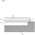
Fig. 5 is a side-view sectional view enlarging a circumferential part of a metal plate and a mold recessed part used in the embodiment of the present invention. - As illustrated in
Fig. 2 , an electronic device of the present embodiment may have asubstrate 10, anelectronic element 80 such as a semiconductor element provided on thesubstrate 10 with aconductor layer 13 to be described later interposed therebetween, and asealing part 20 made of a resin material for sealing theelectronic element 80. As illustrated inFig. 1 , thesealing part 20 may have aninsertion part 22 for inserting a fasteningmember 90 such as a screw. Theinsertion part 22 may be provided in a sealing recessedpart 25 recessed compared with a circumferential region. Theinsertion part 22 may be made of a metal material, and aninsertion hole 22a into which the fasteningmember 90 is inserted may be provided at the center of theinsertion part 22. Theinsertion part 22 may be threaded to engage with the fasteningmember 90. - In the present embodiment, a semiconductor device can be given as an example of the electronic device, and a semiconductor element can be given as an example of the
electronic element 80. However, the present invention is not limited to them, and it is not necessary to use a "semiconductor". - As illustrated in
Fig. 2 , thesubstrate 10 may have ametal plate 11, aninsulating layer 12 provided on themetal plate 11, and aconductor layer 13 provided on theinsulating layer 12. In addition, a circuit may be formed by patterning theconductor layer 13 on theinsulating layer 12. Themetal plate 11 may function as a heatsink. Themetal plate 11 and theconductor layer 13 may be made of copper, for example. - As illustrated in
Fig. 4 , depth D of theinsertion part 22 may correspond to length H of thefastening member 90. The depth D of theinsertion part 22 "corresponds to length H of thefastening member 90" means that the depth D of theinsertion part 22 is shorter than the length H of the fasteningmember 90 by a predetermined length (for example, 0.7 × H ≤ D ≤ 0.9H), and the depth D is set so that there is no problem in inserting the fasteningmember 90 into theinsertion part 22 and fixing the electronic device at a predetermined location. - At least the side surface of the sealing
part 20 and the sealing recessedpart 25 may be exposed to the outside. In addition, the entire side surface and the entire front surface of the sealingpart 20 may be exposed to the outside. "Exposed to the outside" means that there is no frame body surrounding the electronic device, and means that the electronic device is a so-called caseless device. The aspect illustrated in the drawings of the present embodiment is a caseless aspect. - As illustrated in
Fig. 2 , aterminal 70 connected to theelectronic element 80 and protruding to the outside from the front surface of the sealingpart 20 may be provided. In addition, theterminal 70 may be straight without being bent. In the case where theterminal 70 described above is provided, sealing is generally performed by potting in which less pressure is applied. - As illustrated in
Fig. 3 , amold 100 may have a back-surface-side mold 110 and a front-surface-side mold 120 placed on the front surface of the back-surface-side mold 110. The back-surface-side mold 110 and the front-surface-side mold 120 may be connected by afastening member 160. The front-surface-side mold 120 may have a projectingpart 125 corresponding to the sealing recessedpart 25 of the electronic device. - The front-surface-
side mold 120 may have anelastic body 140 such as packing positioned so as to come into contact with a top part of theinsertion part 22. When the front-surface-side mold 120 is fastened to the back-surface-side mold 110 with thefastening member 160, theelastic body 140 is pressed against the top part of theinsertion part 22. As a result, themetal plate 11 is pressed against the back-surface-side mold 110. - The front-surface-
side mold 120 may be provided with anopening 150 for potting resin. Resin sealing is performed by potting resin from theopening 150 of the front-surface-side mold 120 after thesubstrate 10, theelectronic element 80, theinsertion part 22, the terminal 70 and the like are placed in themold 100 - The back-surface-
side mold 110 may have a mold recessedpart 111 facing the back surface of themetal plate 11. In the case of adopting the back-surface-side mold 110 described above, the circumferential part of themetal plate 11 of thesubstrate 10 may come into contact with an edge of the mold recessedpart 111. The circumferential part of themetal plate 11 means part of themetal plate 11 that is within a distance of 1/8 of the length in the lateral direction or the length in the longitudinal direction of themetal plate 11 from the outermost circumference of themetal plate 11. That is, the circumferential part in the lateral direction means part within the distance of 1/8 of the length in the lateral direction, and the circumferential part in the longitudinal direction means part within the distance of 1/8 of the length in the longitudinal direction. In addition, in a case where the length of themetal plate 11 in the lateral direction is equal to or greater than a predetermined length (for example, 24 cm), part of themetal plate 11 within a predetermined distance (for example, within a distance of 3 cm) from the outermost circumference may be the circumferential part. As an example, a region from 0.5 mm to the distance equal to the thickness of themetal plate 11 from the outermost circumference of the metal plate 11 (more specifically, a location at 1 mm from the outermost circumference of the metal plate 11) may come into contact with the edge of the mold recessedpart 111. - As illustrated in
Fig. 5 , themetal plate 11 of thesubstrate 10 may have ametal body part 11a, and a metal thinnedpart 11b provided on the circumference of themetal body part 11a and thinner than themetal body part 11a. In the case of adopting themetal plate 11 having the above-described shape, the metal thinnedpart 11b may be located outward of the circumference of the mold recessedpart 111 when resin is poured into themold 100. Themetal body part 11a may have a substantially quadrangular cross section. The metal thinnedpart 11b may gradually become thinner as it proceeds outward of the circumference. The metal thinnedpart 11b may be gradually thinned on a front-surface side, may be gradually thinned on a back-surface side (seeFig. 5 ), or may be gradually thinned on both the front-surface side and the back-surface side. - In a case where the circumferential part of the
metal plate 11 of thesubstrate 10 is pressed against the edge of the mold recessedpart 111 of the back-surface-side mold 110 with a strong force, a pressing mark is formed on the circumferential part of the back surface of themetal plate 11. That is, in a case where the mold recessedpart 111 as illustrated in the present embodiment is adopted and the circumferential part of themetal plate 11 is pressed against the edge of the mold recessedpart 111 with a strong force, a pressing mark is formed on the circumferential part of the back surface of themetal plate 11. In contrast, in a case where amold 100 not having the mold recessedpart 111 as in the present embodiment is used, it is unlikely that a pressing mark or the like will be formed on the circumferential part of the back surface of themetal plate 11. Therefore, it is highly likely that an electronic device having ametal plate 11 with a pressing mark as described above adopts a mold recessedpart 111. - In addition, in the case of adopting an aspect in which the sealing recessed
part 25 is appropriately provided, the degree of freedom of design can be increased. As an example, in a case where an aspect in which theinsertion part 22 is provided in the sealing recessedpart 25 and the depth D of theinsertion part 22 corresponds to the length H of the fastening member 90 (seeFig. 4 ), the thickness of the sealing recessedpart 25 can be easily adjusted to a thickness corresponding to the length of thefastening member 90 and the length of theinsertion part 22. Therefore, electronic devices of different types and forms can useidentical fastening members 90 by setting the thickness of each sealing recessedpart 25 to substantially an identical value, for example, a value within ± 5% of the average value D0: DO × (1 ± 0.05) . As a result, it is possible to standardize parts, to reduce manufacturing costs, and to eliminate the risk of mix-up of parts in advance. - Next, processes for manufacturing an electronic device (a method for manufacturing an electronic device) according to the present embodiment having the above-described configuration will be described. Any aspect described in "Configuration", which will be an overlapping description and therefore will not be stated, can be applied.
- The
substrate 10 having theelectronic element 80 and the terminal 70 arranged on theconductor layer 13 on a front-surface side and themetal plate 11 on a back-surface side is placed on the back-surface-side mold 110 having the mold recessed part 111 (substrate placing process). At that time, the center of the mold recessedpart 111 and the center of themetal plate 11 may be aligned, and the circumferential part of themetal plate 11 may come into contact with the edge of the mold recessedpart 111. - Next, the
insertion part 22 for inserting thefastening member 90 is placed (insertion part placing process) . Note that the process of placing theinsertion part 22 may be performed simultaneously with or before the process of placing theelectronic element 80 and/or the terminal 70 on theconductor layer 13. - Next, the front-surface-
side mold 120 is placed on the back-surface-side mold 110 so as to cover entirety of thesubstrate 10, and the front-surface-side mold 120 is fixed to the back-surface-side mold 110 by thefastening member 160. By fixing the front-surface-side mold 120 to the back-surface-side mold 110 by thefastening member 160 as described above, thesubstrate 10 is pressed against the back-surface-side mold 110. At that time, by adjusting fastening force of thefastening member 160, magnitude of pressure for pressing thesubstrate 10 against the back-surface-side mold 110 may be adjusted. - Next, resin is poured between the front-
surface mold 100 and the back-surface-side mold 110 for example, by potting (resin inflow process). At that time, themetal plate 11 is pressed against the back-surface-side mold 110 in a state where the circumferential part of themetal plate 11 of thesubstrate 10 is in contact with the edge of the mold recessedpart 111. Therefore, a strong pressure can be applied to themetal plate 11 by the edge of the mold recessedpart 111, and the likelihood that resin will flow to the back surface of themetal plate 11 can be reduced. Note that prior to pouring of resin by potting, themold 100 may be warmed to about 85°C by a preheating unit (preheating plate), and while resin is poured, themold 100 may be warmed by the preheating unit (preheating plate) set at about 75°C. Performing preheating as described above is advantageous in that it is possible to prompt resin to flow to the outer circumference of the sealing recessedpart 25. - In a case where the front-
surface mold 100 has theelastic body 140, in the resin inflow process, theinsertion part 22 for inserting thefastening member 90 is placed on the front surface of thesubstrate 10, and theelastic body 140 of the front-surface-side mold 120 is positioned on the top part of theinsertion part 22. Then, by pressing the top part of theinsertion part 22 by the bottom surface of the projectingpart 125 of the front-surface-side mold 120, thesubstrate 10 is pressed against the back-surface-side mold 110 in a state where the circumferential part of themetal plate 11 is in contact with the edge of the mold recessedpart 111. In this state, resin to be material of the sealingpart 20 is poured into themold 100. By using theelastic body 140 described above, thesubstrate 10 can be pressed against the edge of the mold recessedpart 111 by also using elastic force (repulsive force) of theelastic body 140. As a result, the likelihood that resin will flow to the back surface of themetal plate 11 can be further reduced. - The location where the
metal plate 11 is pressed by a pressing member such as theinsertion part 22 may be peripherally inside the mold recessedpart 111. By pressing themetal plate 11 at the location described above, themetal plate 11 can be pushed in such that themetal plate 11 bends into the mold recessedpart 111, which is advantageous in that the likelihood that resin will flow to the back surface of themetal plate 11 can be further reduced. - The location where the
metal plate 11 is pressed by the pressing member such as theinsertion part 22 may be a plurality of portions intermittently arranged or may be continuous portions. By adopting such an aspect, themetal plate 11 can be more reliably pressed against the back-surface-side mold 110, and the likelihood that resin will flow to the back surface of themetal plate 11 can be further reduced. - In addition, in a case where there is a plurality of portions where the
metal plate 11 is pressed by the pressing member such as theinsertion part 22, the portions may be arranged at equal intervals or may be arranged line-symmetrically or point-symmetrically. By adopting such an aspect, themetal plate 11 can be pressed against the back-surface-side mold 110 in a more balanced manner, and the likelihood that resin will flow to the back surface of themetal plate 11 can be further reduced. - Note that in a case where the sealing
part 20 has a substantially quadrangular shape in plan view, theinsertion part 22 may be provided correspondingly to each side, or theinsertion parts 22 may be provided on a pair of sides facing each other. Note that in a case where the sealingpart 20 has a substantially rectangular shape in plan view, theinsertion parts 22 may be provided on a pair of short sides, or theinsertion parts 22 may be provided on a pair of long sides . Note that a "substantially quadrangular shape in plan view" means an aspect in which sides facing each other are parallel in plan view, and includes an aspect in which a corner part is rounded in plan view. A "substantially rectangular shape in plan view" means an aspect in which sides facing each other are parallel in plan view and there are short sides and long sides, and includes an aspect in which a corner part is rounded in plan view. By appropriately changing the location of theinsertion part 22 according to the size and the shape of the product, the portion of themetal plate 11, pressed by theinsertion part 22 can be appropriately changed, and the likelihood that resin will flow to the back surface of themetal plate 11 can be further reduced. For example, when an aspect in which theinsertion parts 22 are provided on a pair of short sides is adopted (when an aspect in which the circumferential part on the right side surface and the circumferential part on the left side surface inFig. 1 are pressed is adopted) in a case where the sealingpart 20 has a substantially rectangular shape in plan view, this aspect is advantageous in that themetal plate 11 can be pressed against the circumference of the mold recessedpart 111 at portions the length between which is long and where the influence of warping or the like of themetal plate 11 is likely to appear. - In a case where an aspect in which the
metal plate 11 has themetal body part 11a and the metal thinnedpart 11b thinner than themetal body part 11a is adopted, in the resin inflow process, themetal plate 11 may be pressed against the back-surface-side mold 110 in a state where the metal thinnedpart 11b is located outward of the mold recessedpart 111 and themetal body part 11a is in contact with the edge of the mold recessedpart 111. By pressing the thickmetal body part 11a against the edge of the mold recessedpart 111 as described above, the likelihood that resin will flow to the back surface of themetal plate 11 can be further reduced. - This point will be explained. The
metal plate 11 may have themetal body part 11a having a substantially quadrangular cross section and the metal thinnedpart 11b becoming thinner toward the circumference. In a case where the metal thinnedpart 11b is pressed against the edge of the mold recessedpart 111 in a case where themetal plate 11 described above is used, since the shape of the metal thinnedpart 11b is not uniform, resin sometimes flows to the back-surface side of themetal plate 11 through a gap inevitably formed between the metal thinnedpart 11b and the mold recessedpart 111. In this respect, as in the present aspect, by pressing themetal body part 11a against the edge of the mold recessedpart 111, themetal body part 11a having a substantially quadrangular cross section and having a shape close to a uniform shape, the likelihood that resin will flow to the back-surface side of themetal plate 11 can be further reduced. - As described above, when resin is poured into the
mold 100, for example, by potting, the resin is cured at a predetermined temperature to form the sealing part 20 (curing process). - Next, by removing the
mold 100, a caseless electronic device in which the entire side surface and the entire front surface of the sealingpart 20 are exposed to the outside is manufactured. - The description of the embodiment and the disclosure of the drawings described above are merely examples for explaining the invention described in the claims, and the invention described in the claims is not limited by the description of the embodiment or the disclosure of the drawings described above. In addition, the recitation of the claims at the original application is merely an example, and the recitation of the claims can be appropriately changed based on the description of the specification, the drawings, and the like.
-
- 10
- Substrate
- 11
- Metal plate
- 11a
- Metal body part
- 11b
- Metal thinned part
- 20
- Sealing part
- 22
- Insertion part
- 70
- Terminal
- 80
- Electronic element
- 90
- Fastening member
- 110
- Back-surface-side mold
- 111
- Mold recessed part
- 120
- Front-surface-side mold
- 140
- Elastic body
Claims (6)
- A manufacturing method for an electronic device comprising:a step of placing a substrate, which has a metal plate on a back-surface side, on a back-surface-side mold having a mold recessed part;a step of placing a front-surface-side mold on the back-surface-side mold so as to cover the substrate; anda step of pouring resin between the front-surface mold and the back-surface-side mold, while the substrate is pressed against the back-surface-side mold,wherein circumferential part of the metal plate is in contact with an edge of the mold recessed part, when the substrate is pressed against the back-surface-side mold in the step of pouring resin.
- The manufacturing method for an electronic device according to claim 1,
wherein the metal plate has a metal body part and a metal thinned part provided on circumference of the metal body part and thinner than the metal body part
wherein the metal thinned part is located outward of circumference of the mold recessed part and the metal body part is in contact with the edge of the mold recessed part, when the metal plate is pressed against the back-surface-side mold in the step of pouring resin. - The manufacturing method for an electronic device according to claim 1,
wherein an insertion part for inserting a fastening member is placed on a front surface of the substrate,
wherein an elastic body is positioned on a top part of the insertion part, and
wherein the metal plate is pressed against the back-surface-side mold by pressing the elastic body to the top part of the insertion part. - The manufacturing method for an electronic device according to claim 1,
wherein an electronic element is provided on the substrate placed on the back-surface-side mold, and a terminal is connected to the electronic element - An electronic device comprising:a substrate having a metal plate on a back-surface side;an electronic element provided on the substrate; anda sealing part made of a resin material for sealing the electronic element,wherein a back surface of the metal plate is exposed outside from the sealing part, andwherein a pressing mark is formed on a circumferential part of the back surface of the metal plate.
- The electronic device according to claim 5,
wherein an entire side surface, an entire front surface and an entire circumferential part compared with the metal plate in a back surface side of the sealing part are exposed to outside .
Applications Claiming Priority (1)
| Application Number | Priority Date | Filing Date | Title |
|---|---|---|---|
| PCT/JP2016/088619 WO2018122894A1 (en) | 2016-12-26 | 2016-12-26 | Method for manufacturing electronic device, and electronic device |
Publications (2)
| Publication Number | Publication Date |
|---|---|
| EP3561864A1 true EP3561864A1 (en) | 2019-10-30 |
| EP3561864A4 EP3561864A4 (en) | 2020-07-08 |
Family
ID=62107321
Family Applications (1)
| Application Number | Title | Priority Date | Filing Date |
|---|---|---|---|
| EP16916391.2A Pending EP3561864A4 (en) | 2016-12-26 | 2016-12-26 | METHOD FOR PRODUCING AN ELECTRONIC DEVICE AND ELECTRONIC DEVICE |
Country Status (5)
| Country | Link |
|---|---|
| US (1) | US10559478B2 (en) |
| EP (1) | EP3561864A4 (en) |
| JP (1) | JP6321892B1 (en) |
| CN (1) | CN108604576B (en) |
| WO (1) | WO2018122894A1 (en) |
Families Citing this family (1)
| Publication number | Priority date | Publication date | Assignee | Title |
|---|---|---|---|---|
| CN115476457B (en) * | 2022-10-27 | 2026-02-03 | 深圳市联影高端医疗装备创新研究院 | Die and wiring assembly pouring molding method |
Family Cites Families (17)
| Publication number | Priority date | Publication date | Assignee | Title |
|---|---|---|---|---|
| JPH0724273B2 (en) * | 1988-11-09 | 1995-03-15 | 三菱電機株式会社 | Method of manufacturing module for IC card |
| JPH0531246U (en) * | 1991-09-30 | 1993-04-23 | 関西日本電気株式会社 | Semiconductor device |
| JP3315255B2 (en) * | 1994-07-15 | 2002-08-19 | アピックヤマダ株式会社 | Resin molding method for semiconductor device, carrier frame used therefor, and resin molding device |
| US6576496B1 (en) * | 2000-08-21 | 2003-06-10 | Micron Technology, Inc. | Method and apparatus for encapsulating a multi-chip substrate array |
| JP2003347484A (en) * | 2002-05-29 | 2003-12-05 | Sanyo Electric Co Ltd | Hybrid integrated circuit device |
| JP2007165692A (en) * | 2005-12-15 | 2007-06-28 | Denso Corp | Manufacturing method of electronic device |
| KR101391925B1 (en) * | 2007-02-28 | 2014-05-07 | 페어차일드코리아반도체 주식회사 | Semiconductor package and semiconductor package mold for fabricating the same |
| JP4606447B2 (en) * | 2007-09-27 | 2011-01-05 | 三洋電機株式会社 | A method for manufacturing a metal substrate of an intermediate plate. |
| JP4576448B2 (en) | 2008-07-18 | 2010-11-10 | 三菱電機株式会社 | Power semiconductor device |
| JP4825259B2 (en) | 2008-11-28 | 2011-11-30 | 三菱電機株式会社 | Power semiconductor module and manufacturing method thereof |
| JP5171777B2 (en) | 2009-09-30 | 2013-03-27 | 三菱電機株式会社 | Power semiconductor device |
| JP4755292B1 (en) * | 2010-05-11 | 2011-08-24 | 株式会社サンエー | Jig and molding method of semiconductor module |
| JP6041795B2 (en) | 2013-12-10 | 2016-12-14 | 三菱電機株式会社 | Semiconductor device |
| JP6249829B2 (en) * | 2014-03-10 | 2017-12-20 | 三菱電機株式会社 | Semiconductor device and manufacturing method thereof |
| JP6338406B2 (en) * | 2014-03-11 | 2018-06-06 | エイブリック株式会社 | Manufacturing method of semiconductor device |
| JP2015185835A (en) * | 2014-03-26 | 2015-10-22 | 株式会社デンソー | Semiconductor device and manufacturing method thereof |
| WO2015151235A1 (en) * | 2014-04-01 | 2015-10-08 | 富士電機株式会社 | Semiconductor device |
-
2016
- 2016-12-26 JP JP2017549825A patent/JP6321892B1/en active Active
- 2016-12-26 US US15/757,832 patent/US10559478B2/en active Active
- 2016-12-26 CN CN201680060719.1A patent/CN108604576B/en active Active
- 2016-12-26 EP EP16916391.2A patent/EP3561864A4/en active Pending
- 2016-12-26 WO PCT/JP2016/088619 patent/WO2018122894A1/en not_active Ceased
Also Published As
| Publication number | Publication date |
|---|---|
| WO2018122894A1 (en) | 2018-07-05 |
| US10559478B2 (en) | 2020-02-11 |
| CN108604576B (en) | 2021-07-09 |
| JP6321892B1 (en) | 2018-05-09 |
| EP3561864A4 (en) | 2020-07-08 |
| JPWO2018122894A1 (en) | 2018-12-27 |
| US20180342406A1 (en) | 2018-11-29 |
| CN108604576A (en) | 2018-09-28 |
Similar Documents
| Publication | Publication Date | Title |
|---|---|---|
| TW494558B (en) | Semiconductor device having lead terminals bent in J-shape | |
| EP3499560A1 (en) | Semiconductor module and method for producing the same | |
| CN110800093B (en) | Circuit device, method for manufacturing circuit device, and connector | |
| TW201233276A (en) | Method of manufacturing electronic component embedded rigid-flexible printed circuit board | |
| US10559478B2 (en) | Method for manufacturing electronic device and electronic device | |
| KR20190087357A (en) | Composite thermal conductive element | |
| CN108538728B (en) | Method of manufacturing semiconductor device | |
| KR101842888B1 (en) | Chip antenna and production method thereof | |
| CN101997210A (en) | Film-shaped electrically-connecting body and manufacture method thereof | |
| US11353349B2 (en) | Flow-rate sensor | |
| US10741480B2 (en) | Leadframe with sockets for solderless pins | |
| US10347555B2 (en) | Electronic device and method for manufacturing electronic device | |
| EP3121896A1 (en) | Chip antenna | |
| JP6810601B2 (en) | Manufacturing method of electronic device | |
| JP6370617B2 (en) | Chip antenna | |
| CN104517925B (en) | Leads of semiconductor device frame | |
| CN112369129B (en) | Electronic Controls | |
| CN107624003A (en) | A kind of flexible PCB and its processing method, mobile terminal | |
| JP2019007441A (en) | Igniter | |
| JP4999492B2 (en) | Manufacturing method of lead frame for semiconductor device and semiconductor device using the same | |
| TWI279900B (en) | Conductor frame for an electronic component and method for the production thereof | |
| JP2014192323A (en) | Substrate and method of manufacturing substrate | |
| JP2015019043A (en) | Electric power supply device | |
| JP2006066600A (en) | Printed board | |
| JP2006216750A (en) | Electronic component sealing method |
Legal Events
| Date | Code | Title | Description |
|---|---|---|---|
| STAA | Information on the status of an ep patent application or granted ep patent |
Free format text: STATUS: UNKNOWN |
|
| STAA | Information on the status of an ep patent application or granted ep patent |
Free format text: STATUS: THE INTERNATIONAL PUBLICATION HAS BEEN MADE |
|
| PUAI | Public reference made under article 153(3) epc to a published international application that has entered the european phase |
Free format text: ORIGINAL CODE: 0009012 |
|
| STAA | Information on the status of an ep patent application or granted ep patent |
Free format text: STATUS: REQUEST FOR EXAMINATION WAS MADE |
|
| 17P | Request for examination filed |
Effective date: 20180326 |
|
| AK | Designated contracting states |
Kind code of ref document: A1 Designated state(s): AL AT BE BG CH CY CZ DE DK EE ES FI FR GB GR HR HU IE IS IT LI LT LU LV MC MK MT NL NO PL PT RO RS SE SI SK SM TR |
|
| AX | Request for extension of the european patent |
Extension state: BA ME |
|
| DAV | Request for validation of the european patent (deleted) | ||
| DAX | Request for extension of the european patent (deleted) | ||
| A4 | Supplementary search report drawn up and despatched |
Effective date: 20200609 |
|
| RIC1 | Information provided on ipc code assigned before grant |
Ipc: H01L 23/28 20060101ALI20200603BHEP Ipc: H01L 23/31 20060101ALI20200603BHEP Ipc: H01L 21/56 20060101ALI20200603BHEP Ipc: B29C 39/10 20060101AFI20200603BHEP Ipc: H01L 23/367 20060101ALN20200603BHEP Ipc: H01L 23/16 20060101ALI20200603BHEP Ipc: B29L 31/34 20060101ALN20200603BHEP Ipc: B29K 705/00 20060101ALN20200603BHEP |