EP3561683A1 - Setting identification information in a communication system - Google Patents
Setting identification information in a communication system Download PDFInfo
- Publication number
- EP3561683A1 EP3561683A1 EP19166027.3A EP19166027A EP3561683A1 EP 3561683 A1 EP3561683 A1 EP 3561683A1 EP 19166027 A EP19166027 A EP 19166027A EP 3561683 A1 EP3561683 A1 EP 3561683A1
- Authority
- EP
- European Patent Office
- Prior art keywords
- slave
- information
- identification information
- master device
- unique information
- Prior art date
- Legal status (The legal status is an assumption and is not a legal conclusion. Google has not performed a legal analysis and makes no representation as to the accuracy of the status listed.)
- Granted
Links
Images



Classifications
-
- G—PHYSICS
- G06—COMPUTING OR CALCULATING; COUNTING
- G06F—ELECTRIC DIGITAL DATA PROCESSING
- G06F13/00—Interconnection of, or transfer of information or other signals between, memories, input/output devices or central processing units
- G06F13/38—Information transfer, e.g. on bus
- G06F13/42—Bus transfer protocol, e.g. handshake; Synchronisation
- G06F13/4282—Bus transfer protocol, e.g. handshake; Synchronisation on a serial bus, e.g. I2C bus, SPI bus
-
- G—PHYSICS
- G06—COMPUTING OR CALCULATING; COUNTING
- G06F—ELECTRIC DIGITAL DATA PROCESSING
- G06F11/00—Error detection; Error correction; Monitoring
- G06F11/07—Responding to the occurrence of a fault, e.g. fault tolerance
- G06F11/08—Error detection or correction by redundancy in data representation, e.g. by using checking codes
- G06F11/10—Adding special bits or symbols to the coded information, e.g. parity check, casting out 9's or 11's
-
- B—PERFORMING OPERATIONS; TRANSPORTING
- B60—VEHICLES IN GENERAL
- B60R—VEHICLES, VEHICLE FITTINGS, OR VEHICLE PARTS, NOT OTHERWISE PROVIDED FOR
- B60R16/00—Electric or fluid circuits specially adapted for vehicles and not otherwise provided for; Arrangement of elements of electric or fluid circuits specially adapted for vehicles and not otherwise provided for
- B60R16/02—Electric or fluid circuits specially adapted for vehicles and not otherwise provided for; Arrangement of elements of electric or fluid circuits specially adapted for vehicles and not otherwise provided for electric constitutive elements
-
- B—PERFORMING OPERATIONS; TRANSPORTING
- B60—VEHICLES IN GENERAL
- B60R—VEHICLES, VEHICLE FITTINGS, OR VEHICLE PARTS, NOT OTHERWISE PROVIDED FOR
- B60R16/00—Electric or fluid circuits specially adapted for vehicles and not otherwise provided for; Arrangement of elements of electric or fluid circuits specially adapted for vehicles and not otherwise provided for
- B60R16/02—Electric or fluid circuits specially adapted for vehicles and not otherwise provided for; Arrangement of elements of electric or fluid circuits specially adapted for vehicles and not otherwise provided for electric constitutive elements
- B60R16/023—Electric or fluid circuits specially adapted for vehicles and not otherwise provided for; Arrangement of elements of electric or fluid circuits specially adapted for vehicles and not otherwise provided for electric constitutive elements for transmission of signals between vehicle parts or subsystems
-
- G—PHYSICS
- G06—COMPUTING OR CALCULATING; COUNTING
- G06F—ELECTRIC DIGITAL DATA PROCESSING
- G06F13/00—Interconnection of, or transfer of information or other signals between, memories, input/output devices or central processing units
- G06F13/10—Program control for peripheral devices
- G06F13/12—Program control for peripheral devices using hardware independent of the central processor, e.g. channel or peripheral processor
- G06F13/122—Program control for peripheral devices using hardware independent of the central processor, e.g. channel or peripheral processor where hardware performs an I/O function other than control of data transfer
-
- G—PHYSICS
- G06—COMPUTING OR CALCULATING; COUNTING
- G06F—ELECTRIC DIGITAL DATA PROCESSING
- G06F13/00—Interconnection of, or transfer of information or other signals between, memories, input/output devices or central processing units
- G06F13/14—Handling requests for interconnection or transfer
- G06F13/16—Handling requests for interconnection or transfer for access to memory bus
- G06F13/1668—Details of memory controller
-
- G—PHYSICS
- G06—COMPUTING OR CALCULATING; COUNTING
- G06F—ELECTRIC DIGITAL DATA PROCESSING
- G06F7/00—Methods or arrangements for processing data by operating upon the order or content of the data handled
- G06F7/58—Random or pseudo-random number generators
- G06F7/588—Random number generators, i.e. based on natural stochastic processes
-
- G—PHYSICS
- G06—COMPUTING OR CALCULATING; COUNTING
- G06F—ELECTRIC DIGITAL DATA PROCESSING
- G06F9/00—Arrangements for program control, e.g. control units
- G06F9/06—Arrangements for program control, e.g. control units using stored programs, i.e. using an internal store of processing equipment to receive or retain programs
- G06F9/30—Arrangements for executing machine instructions, e.g. instruction decode
- G06F9/38—Concurrent instruction execution, e.g. pipeline or look ahead
- G06F9/3877—Concurrent instruction execution, e.g. pipeline or look ahead using a secondary processor, e.g. coprocessor
Definitions
- the present invention relates to a communication system.
- Various loads such as lamps and power windows are mounted on vehicles such as passenger cars and freight cars.
- a technique has been proposed for controlling the loads by using communication between a slave device to which a plurality of loads is connected and a master device controlling a plurality of slave devices.
- ID identification information
- the master device sends an ID to the slave device every time when a slave device not set with ID is connected to the in-vehicle LAN, and the slave device stores the ID.
- Patent Literature 1 JP 2010-184575 A
- the present invention has been made in view of the above-described background, and it is an object of the present invention to provide a communication system capable of shortening setting time of identification information and reducing erroneous setting.
- a communication system including:
- the communication system wherein a plurality of types of slave device groups each including the plurality of slave devices are provided, wherein the master device is provided for each of the plurality of slave device groups, and includes a switch provided for each of the plurality of slave device groups and supplying power to the corresponding slave device group, and wherein the master device turns on the switches sequentially and causes the first setting unit to sequentially set the identification information of the plurality of slave devices for each of the slave device groups.
- the communication system wherein the first setting unit sets the identification information corresponding to each piece of the random information, wherein the master device includes a third transmitting unit that adds the set identification information to the random information and transmits the random information, and wherein the plurality of slave devices have a second setting unit that sets the received identification information as its identification information when receiving the random information generated by itself.
- the communication system wherein a plurality of the master devices is installed in a vehicle, and wherein the identification information includes installation information indicating an installation position of the master device in the vehicle.
- the slave device generates the random information if its own identification information is predetermined initial identification information.
- the communication system wherein the first transmission unit adds the initial identification information to the random information and transmits the added random information, and wherein upon receiving the initial identification information, the master device causes the first setting unit to set the identification information.
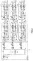
- FIG. 1 is a block diagram showing an in-vehicle network 1 as a communication system of the present invention.
- FIG. 2 is a block diagram showing a configuration of a master device 2 and a slave device 3 constituting the in-vehicle network 1 shown in FIG. 1 .
- the in-vehicle network 1 shown in FIG. 1 is mounted in a vehicle 10.
- the in-vehicle network 1 includes a plurality of master devices 2 and a plurality of slave devices 3.
- the plurality of master devices 2 are arranged in each area of the vehicle 10.
- the master devices 2 are disposed at five locations, the center of the front of the vehicle 10, the right side of the front, the left side of the front, the right side of the rear, and the left side of the rear.
- the five master devices 2 are communicably connected to each other through a communication line L1. Further, the master devices 2 are connected to each other via a +B power supply line L2 connected to a battery (not shown), and power is supplied via the +B power supply line L2.
- each of the five master devices 2 is communicably connected to a plurality of slave devices 3 arranged in the own area through a communication line L1.
- the master device 2 and the slave devices 3 are connected one to many.
- the master device 2 controls the operations of the plurality of slave devices 3 by communicating with the plurality of slave devices 3.
- the slave device 3 is connected to a plurality of loads 20 ( FIG. 2 ) such as lamps, seat motors, door motors and the like disposed in the own area, and controls the driving of the loads 20 in accordance with communication with the master device 2.
- the plurality of slave devices 3 is provided separately for +B, for ACC, and for IG.
- the slave device 3 for +B is connected to the loads 20 that can be driven at all times.
- a plurality of slave devices 3 for +B is provided, and the plurality of slave devices 3 for +B constitutes a slave device group 301 for +B.
- the slave device 3 for ACC is connected to the loads 20 which can be driven when an accessory is used.
- a plurality of slave devices 3 for ACC is provided, and the plurality of ACC slave devices 3 constitutes a slave device group 302 for ACC.
- the slave device 3 for IG is connected to the loads 20 that can be driven when using an ignition.
- a plurality of slave devices 3 for IG is provided, and the plurality of slave devices 3 for IG constitutes a slave device group 303 for IG.
- the plurality of master devices 2 has the same configuration, and each of the plurality of master devices 2 has an interface (hereinafter referred to as I/F) 21, a power supply circuit 22, a plurality of local SWs 23, a microcomputer 24, a semiconductor relay 25 for +B as a switch, a semiconductor relay 26 for ACC, and a semiconductor relay 27 for IG.
- I/F interface
- the I/F 21 is a communication interface for communicating with another master device 2 and a plurality of slave devices 3.
- the I/F 21 is an interface capable of inputting and outputting signals corresponding to various communications (CAN, LIN, and other communication methods).
- the power supply circuit 22 is a circuit that generates a power supply for the microcomputer 24 to be described later from the power supplied from the +B power supply line L2 and supplies power to the microcomputer 24.
- the local SW 23 is operated by the user to operate the load 20.
- the microcomputer 24 is composed of a well-known CPU (Central Processing Unit) 24A and a flash ROM (Read Only Memory) 24B.
- the CPU 24A controls the entire master device 2 and performs various processes according to the processing program.
- the flash ROM 24B is a memory for storing the ID of the slave device 3 connected to the master device 2, the program of processing to be executed by the CPU 24A, and the like.
- the semiconductor relays 25 to 27 are provided corresponding to the plurality of slave device groups 301 to 303.
- the semiconductor relay 25 for +B is connected to the slave device 3 for +B via the +B power supply line L3.
- the semiconductor relay 25 for +B is turned on when a drive signal is output from the microcomputer 24, and supplies power from the +B power supply line L2 to the slave device 3 for +B via the +B power supply line L3.
- the semiconductor relay 26 for ACC is connected to the slave device 3 for ACC via the ACC power supply line L4.
- the semiconductor relay 26 for ACC is turned on when a drive signal is output from the microcomputer 24, and supplies power from the +B power supply line L2 to the slave device 3 for ACC via the ACC power supply line L4.
- the semiconductor relay 27 for IG is connected to the slave device 3 for IG via the IG power supply line L5.
- the semiconductor relay 27 for IG turns on when a drive signal is output from the microcomputer 24, and supplies power from the +B power supply line L2 to the slave device 3 for IG via the IG power supply line L5.
- the +B power supply line L3, the ACC power supply line L4, and the IG power supply line L5 are branched into two and are connected to the two slave devices 3, but the present invention is not limited to this.
- the +B power supply line L3, the ACC power supply line L4, and the IG power supply line L5 may be branched into three or more and may be connected to three or more slave devices 3.
- the semiconductor relays 25 to 27 have a current detection function for detecting a current flowing in the semiconductor relays 25 to 27, and the detected currents are input to the microcomputer 24.
- the plurality of slave devices 3 has the same configuration and each has an I/F 31, a power supply circuit 32, a microcomputer 33, a plurality of local SWs 34, and a plurality of semiconductor relays CH1 to CH8.
- the I/F 31 is an interface for communicating with the master device 2, and capable of inputting and outputting signals corresponding to various communications (CAN, LIN, and other communication methods).
- the power supply circuit 32 is a circuit that generates a power supply for a microcomputer 33 to be described later from power supplied from the +B power supply line L3, the ACC power supply line L4, and the IG power supply line L5 and supplies power to the microcomputer 33.
- the microcomputer 33 is composed of a CPU 33A and a flash ROM 33B.
- the CPU 33A controls the entire slave device 3 and performs various processes according to the processing program.
- the flash ROM 33B is a memory for storing an initial ID, a program, a variable, and a setting value of processing to be executed by the CPU 33A, and in the initial state, the same contents are written in all the slave devices 3.
- the initial ID is a temporary ID, and a transmission initial ID and a reception initial ID are set.
- the processing program of the CPU 33A includes a communication program for communicating with the master device 2 connected via the communication line L1 and a system operation program necessary for system operation.
- the operation program of the load 20 is not written in the flash ROM 33B in the initial state, but is written after setting the ID.
- the plurality of local SWs 34 are connected to the microcomputer 33 and input ON/OFF information to the microcomputer 33.
- the plurality of semiconductor relays CH1 to CH8 are connected between the microcomputer 33 and the loads 20, respectively, and are turned on and off in accordance with a drive signal from the microcomputer 33.
- the semiconductor relays CH1 to CH8 in the slave device 3 for +B turn on the power from the +B power supply line L3 is supplied to the loads 20.
- the semiconductor relays CH1 to CH8 in the slave device 3 for ACC are turned on, the power from the ACC power supply line L4 is supplied to the loads 20.
- the semiconductor relays CH1 to CH8 in the slave device 3 for IG are turned on, the power from the IG power supply line L5 is supplied to the loads 20.
- the semiconductor relays CH1 to CH8 have a current detection function for detecting the current flowing in the semiconductor relays CH1 to CH8, and the detected currents are input to the microcomputer 33.
- the number of the semiconductor relays CH1 to CH8 provided in the slave device 3 is eight as an example, but the present invention is not limited to this and any number may be used. All the slave devices 3 have the same number of semiconductor relays CH1 to CH8.
- slave unique information generation request/ slave unique information After ID setting: load control information bit7 bit6 bit5 bit4 bit3 bit2 bit1 bit0 Before ID setting slave unique information generation request Y:1 N:0 slave unique information 00000000 ⁇ 11111111 After ID setting CH8 ON:1 CH7 ON:1 CH6 ON:1 CH5 ON:1 CH4 ON:1 CH3 ON:1 CH2 ON:1 CH1 ON:1 CH8 OFF:0 CH7 OFF:0 CH6 OFF:0 CH5 OFF:0 CH4 OFF:0 CH3 OFF:0 CH2 OFF:0 CH1 OFF:0
- the first bit10 to bit0 represents the identification information (ID) of the slave device 3.
- ID the identification information
- the identification information is allocated to all the slave devices 3 arranged in the vehicle 10 without overlapping.
- the identification information is composed of drive power information, installation information, transmission/reception information, and slave type information.
- Bit10 to bit9 are allocated to the drive power information, and become “01” if the slave device 3 is connected to the +B power supply line L3, "10” if connected to the ACC power supply line L4, and "11” if connected to the IG power supply line L5.
- Bit8 to bit5 are allocated to the installation information.
- Bit8 to bit7 represent installation positions in the traveling direction of the vehicle, and become “01” if the installation position of the slave device 3 is on the front side of the vehicle, “10” if on the rear side, and “11” if at the center in the traveling direction.
- Bit6 to bit5 represent installation positions in the left-right direction of the vehicle 10, and become “01” if the installation position of the slave device 3 is on the right side of the vehicle 10, "10” in the case of the left side, and “11” in the case of the center in the left-right direction.
- Bit4 is allocated to the transmission/reception information, becomes “1" when the slave device 3 transmits to the master device 2, and becomes “0" when the slave device 3 receives from the master device 2.
- Bit3 to bit0 are allocated to the slave type information.
- the slave type information is information that is allocated without overlapping with a plurality of slave devices 3 connected to the same master device 2 (but may overlap between the slave devices 3 connected to different master devices 2).
- Bit7 to bit0 following the ID indicate load control information after ID setting.
- Bit 7 to bit 0 are allocated to the semiconductor relays CH8 to CH1 respectively.
- each bit n (n is any integer from 0 to 7) is “0”, it represents “off” of the semiconductor relay CH n+1 assigned to the bit n.
- each bit n (n is any integer from 0 to 7) is “1”, it represents "on” of the semiconductor relay CH n+1 assigned to the bit n.
- bit 7 indicates the presence or absence of a slave unique information generation request, which will be described later, and bit 6 to bit 0 indicate slave unique information described later.
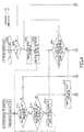
- the ID setting operation of the in-vehicle network 1 having the above-described configuration will be described with reference to the flowcharts of FIGS. 3 to 5 .
- the same initial ID in the initial state (ID is not set), the same initial ID (initial reception ID, initial transmission ID) is set in all the slave devices 3 and stored in the ID area of the flash ROM 33B.
- IDs set in the slave device 3 There are two types of IDs set in the slave device 3: a reception ID and a transmission ID, but since the difference between the two is only the transmission/reception information (bit4 of ID) as shown in Table 1, If either is determined, the transmission/reception ID is naturally determined.
- the setting of the reception ID will be described, and as the initial reception ID, it is assumed that "00000001111" which is "0" for bit10 to bit4 and "1" for bit3 to bit0 is set as shown in the following Table 2.
- installation information is previously stored in the flash ROM 24B or the like in all the master devices 2.
- the flash ROM 24B of the master device 2 installed on the front right side of the vehicle 10 "0101" is previously stored as installation information.
- the microcomputer 24 of the master device 2 executes the ID setting process shown in FIG. 3 after activation, performs ID setting process for +B (step S1), ID setting process for ACC (step S2), and ID setting process for IG (step S3) sequentially.
- the ID setting process for +B is a process of setting the ID of the slave device 3 for +B.
- the ID setting process for ACC is a process of setting the ID of the slave device 3 for ACC.
- the ID setting process for the IG is a process for setting the ID of the slave device 3 for IG.
- the master device 2 turns on the semiconductor relay 25 for +B (step S11 in FIG. 4 ). Power is supplied to the slave device 3 for +B in response to turning on of the semiconductor relay 25 for +B.
- the microcomputer 33 of the slave device 3 for +B (hereinafter sometimes simply referred to as the slave device 3) is activated when power is supplied and executes the ID setting process shown in FIG. 4 .
- the slave device 3 first reads the ID stored in the ID area of the flash ROM 33B (step S201). Next, the slave device 3 judges whether or not the read ID is the initial ID "00000001111" (step S202).
- the slave device 3 If the read ID is not the initial ID (N in step S202), the slave device 3 immediately determines that the ID has already been set and ends the ID setting process. On the other hand, if the read ID is the initial ID (Y in step S202), the CPU 33A of the slave device 3 functions as a generation unit and generates 7-bit slave unique information (random information) (step S203).
- step S203 the slave device 3 executes a generation program such as a PN code typified by an M series code, for example, to generate a random bit string.
- a generation program such as a PN code typified by an M series code, for example, to generate a random bit string.
- the CPU 33A of the slave device 3 functions as a first transmission unit, gives an initial ID, and transmits the slave unique information generated in step S203 (step S204). For example, if "0111100" is generated as the slave unique information, the slave device 3 transmits a signal of a bit string shown in Table 3 below. That is, the ID is "00000001111” (initial ID), the bit 7 representing slave unique information generation request is "0" in the byte, and the bit6 toO representing slave inherent information in the byte is "0111100".
- Each slave device 3 executes step S204, whereby the slave unique information generated by each slave device 3 is transmitted to the master device 2.
- the master device 2 When the master device 2 receives the slave unique information assigned with the initial ID within a predetermined time T1 (Y in step S12) after turning on the semiconductor relay 25 for +B in step S11, the master device 2 proceeds to the next step S13.
- the master device 2 can receive the slave unique information from all the slave devices 3 connected to the master device 2 within a reception cycle (for example, 100 ms). In step S13, the master device 2 determines whether there is a match with the plurality of slave unique information received within the reception cycle.
- step S13 if there is a match among even one set of slave unique information (Y in step S13), the CPU 24A of the master device 2 functions as a second transmission unit and transmits slave unique information generation request (regeneration command) (step S14), and returns to step S12.
- Table 4 shows an example of the slave unique information transmitted from the three slave devices 3A to 3C connected to the master device 2.
- the slave unique information generated by each of the slave devices 3A and 3C matches.
- a signal of a bit string shown in the following Table 5 is transmitted. That is, the ID is "00000001111" (initial ID), the bit7 representing slave unique information generation request in the byte is "1", and the bits 6 to 0 representing slave unique information in the byte are "0".
- the slave device 3 When the slave device 3 receives the slave unique information generation request within the predetermined time T2 after transmitting the slave unique information (Y in step S205), the slave device 3 returns to step S203 again and regenerates the slave unique information.
- Table 6 shows an example of the slave unique information transmitted from the three slave devices 3A to 3C connected to the master device 2. As shown in Table 6, all the slave unique information generated by each of the slave devices 3A to 3C is different from each other.
- the CPU 24A of the master device 2 functions as a first setting unit and a third transmission unit, sets an ID corresponding to the discrete slave unique information, and transmits set ID and the slave unique information corresponding to the set ID.
- Step S15 will be described in detail.
- the master device 2 associates the received slave unique information with the slave type information.
- the slave type information is assigned in order from "1" in ascending order of slave unique information.
- the slave unique information "0111100” transmitted from the slave apparatus 3A is the lowest, so that the lowest slave type information "0001" is associated.
- the slave unique information "1011010” transmitted from the slave device 3B is the next low, "0010” obtained by adding 1 to "0001” is associated as slave type information.
- the slave unique information "1101001” transmitted from the slave device 3C is the next low, "0011” obtained by adding 1 to "0010” is associated as slave type information.
- the master device 2 transmits driving power information, installation information, and transmission/reception information "0" to each of slave type information and transmits slave unique information corresponding to each ID.
- the master device 2 assigns "01" indicating the +B power supply as the drive power information. Further, the master device 2 assigns pre-stored installation information "0101".
- the slave device 3 Upon receiving the same slave unique information as the slave unique information generated and transmitted by the slave device 3 within the predetermined time T2 (Y in step S206 of FIG. 5 ), the slave device 3 erases the initial ID from the ID area of the flash ROM 33B (Step S207). When the erasing of the ID area of the flash ROM 33B succeeds (Y in step S208), the CPU 33A of the slave device 3 functions as a second setting unit, and writes the ID transmitted together with the same slave unique information as the slave unique information transmitted by the CPU 33A in the flash ROM 33B as a reception ID (step S209).
- the slave device 3 transmits the slave unique information with the written ID (Step S211), and ends the process.
- step S15 When the ID and the slave unique information received from all the slave devices 3 and the ID and the slave unique information transmitted in step S15 match within a predetermined time T3 from step S15 in FIG. 4 (step Y in S16), the ID setting process for +B is terminated.
- the slave device 3 cannot receive the same slave unique information as the slave unique information transmitted within the predetermined time T2 (N in Step S 206), when the erasure of the flash ROM 33B fails (N in Step S 208), or when writing of the ID fails (N in step S210), the slave unique information is transmitted with the initial ID (step S212), and the ID setting process is terminated.
- the master device 2 When the master device 2 cannot receive the initial ID within the predetermined time T1 (N in step S12 in FIG. 4 ), or when the master device 2 cannot receive the ID and the slave unique information matching the ID and the slave unique information transmitted in step S15 within the predetermined time T3 (N in step S16), the ID setting is canceled (step S17), and the ID setting process for +B is terminated.
- the ID setting process for ACC and the ID setting process for IG will be described.
- the master device 2 is similar to the setting process for +B, the master device 2 will be briefly described.
- the master device 2 turns on the semiconductor relay 26 for ACC and the semiconductor relay 27 for IG, instead of turning on the semiconductor relay 25 for +B in
- the slave devices 3 execute the above-described ID setting process.
- the master device 2 executes the same processing as the steps S11 to S16 of the ID setting process for +B.
- the master device 2 instead of providing "01" indicating the +B power supply in step S15 as drive power information, the master device 2 adds "10", "11” indicating the ACC power supply and the IG power supply.
- each of the plurality of slave devices 3 generates the slave unique information which is random information when setting the ID, and transmits the generated slave unique information to the master device 2.
- the master device 2 sets an ID based on each slave unique information, and if the slave unique information received from the plurality of slave devices 3 matches, the master device 2 transmits a slave unique information generation request which is an instruction to regenerate the slave unique information.
- the slave device 3 receives the generation request, the slave device 3 re-creates the slave unique information.
- a plurality of slave devices 3 having a plurality of types (+B, ACC, IG) of different supply timing of the power supply is provided.
- the master device 2 supplies power to the plurality of slave devices 3 in turn for each type and sets IDs of the plurality of slave devices 3 in order of power supply for each type.
- ID setting is sequentially performed for each type of power supply, so the probability that the slave unique information coincides becomes low, and the setting time of the ID can be shortened.
- the master device 2 sets the ID corresponding to each slave unique information.
- the master device 2 adds the ID set to the slave unique information and transmits it to the plurality of slave devices 3.
- the plurality of slave devices Upon receiving the random information generated by the plurality of slave devices, the plurality of slave devices sets the received identification information as its own identification information.
- the slave device 3 can also set the ID corresponding to the slave unique information set by the master device 2.
- a plurality of master devices 2 is installed in the vehicle 10, and the ID includes information indicating the installation position of the master device 2 in the vehicle.
- the ID includes information indicating the installation position of the master device 2 in the vehicle.
- the slave device 3 creates slave unique information if its own ID is a predetermined initial ID. Thereby, ID can be set automatically.
- the slave device 3 adds the initial ID to the slave unique information and transmits the slave unique information, and when receiving the initial ID, the master device 2 sets the ID. Thereby, ID can be set automatically.
- the ID includes 4-bit slave type information different from the 7-bit slave unique information, but the present invention is not limited to this.
- the same 4-bit slave unique information as the slave type information may be generated and added as the slave type information.
- the number of the slave devices 3 it is preferable to generate the slave unique information having a larger number of bits than the slave type information like this embodiment. Thereby, the probability of matching of the generated slave unique information is lowered, and the number of regeneration of the slave unique information is reduced, so that the ID setting can be shortened.
- the master device 2 sequentially supplies the power to the slave devices 3 for +B, ACC, and IG, and sets the IDs in order, but the present invention is not limited to this.
- the master device 2 may simultaneously supply power to the slave devices 3 for +B, ACC, and IG, and set the IDs at the same time.
- the number of the slave devices 3 is large, it is better to set the IDs in order like the present embodiment, since the probability of matching of the slave unique information decreases, the number of regeneration of the slave unique information is reduced, and it is possible to shorten the ID setting.
Landscapes
- Engineering & Computer Science (AREA)
- Theoretical Computer Science (AREA)
- General Physics & Mathematics (AREA)
- Physics & Mathematics (AREA)
- General Engineering & Computer Science (AREA)
- Mechanical Engineering (AREA)
- Software Systems (AREA)
- Computational Mathematics (AREA)
- Mathematical Optimization (AREA)
- Pure & Applied Mathematics (AREA)
- Mathematical Analysis (AREA)
- Quality & Reliability (AREA)
- Small-Scale Networks (AREA)
- Remote Monitoring And Control Of Power-Distribution Networks (AREA)
Abstract
Description
- The present invention relates to a communication system.
- Various loads such as lamps and power windows are mounted on vehicles such as passenger cars and freight cars. A technique has been proposed for controlling the loads by using communication between a slave device to which a plurality of loads is connected and a master device controlling a plurality of slave devices.
- In the above technique, it is necessary to set identification information (ID) in a plurality of slave devices to which a plurality of loads is connected, respectively.
- As a method for setting the ID, for example, one described in
Patent Literature 1 has been proposed. In the above-described ID setting method, the master device sends an ID to the slave device every time when a slave device not set with ID is connected to the in-vehicle LAN, and the slave device stores the ID. - However, since the ID is set every connection of the slave device, there is a problem that it takes time to set the ID. Also, since the order of IDs sent by the master device to the slave device is fixed, there is also a problem that if the connection order of the slave device to the in-vehicle LAN is different, an ID different from the original ID is set.
- Patent Literature 1:
JP 2010-184575 A - The present invention has been made in view of the above-described background, and it is an object of the present invention to provide a communication system capable of shortening setting time of identification information and reducing erroneous setting.
- According to a first aspect of the present invention, there is provided a communication system including:
- a plurality of slave devices; and
- a master device that communicates with the plurality of slave devices,
- wherein each of the plurality of slave devices includes: a generation unit that generates random information when setting identification information; and a first transmission unit that transmits generated random information,
- wherein the master device includes: a first setting unit that sets the identification information based on each piece of the random information when all the pieces of the random information received from the plurality of slave devices are different; and a second transmission unit that transmits a regeneration command of the random information if the random information received from the plurality of slave devices includes information equivalent to each other, and
- wherein the generation unit generates the random information again upon receiving the regeneration command.
- Preferably, there is provided the communication system,
wherein a plurality of types of slave device groups each including the plurality of slave devices are provided,
Wherein the master device is provided for each of the plurality of slave device groups, and includes a switch provided for each of the plurality of slave device groups and supplying power to the corresponding slave device group, and
wherein the master device turns on the switches sequentially and causes the first setting unit to sequentially set the identification information of the plurality of slave devices for each of the slave device groups. - Preferably, there is provided the communication system,
wherein the first setting unit sets the identification information corresponding to each piece of the random information,
wherein the master device includes a third transmitting unit that adds the set identification information to the random information and transmits the random information, and
wherein the plurality of slave devices have a second setting unit that sets the received identification information as its identification information when receiving the random information generated by itself. - Preferably, there is provided the communication system,
wherein a plurality of the master devices is installed in a vehicle, and
wherein the identification information includes installation information indicating an installation position of the master device in the vehicle. - Preferably, there is provided the communication system,
wherein the slave device generates the random information if its own identification information is predetermined initial identification information. - Preferably, there is provided the communication system,
wherein the first transmission unit adds the initial identification information to the random information and transmits the added random information, and
wherein upon receiving the initial identification information, the master device causes the first setting unit to set the identification information. - According to the aspect described above, it is unnecessary to assign the identification information every time the slave device is connected, therefore it is possible to shorten the setting time of the identification information and reduce the erroneous setting.
-
-
FIG. 1 is a block diagram showing an in-vehicle network as a communication system of the present invention; -
FIG. 2 is a block diagram showing a configuration of a master device and a slave device that constitute the in-vehicle network shown inFIG. 1 ; -
FIG. 3 is a flowchart showing an ID setting process procedure executed by the master device shown inFIG. 1 ; -
FIG. 4 is a flowchart showing an ID setting process procedure for +B executed by the master device and the slave device shown inFIG. 1 ; and -
FIG. 5 is a flowchart showing an ID setting process procedure for +B executed by the master device and the slave device shown inFIG. 1 . - Hereinafter, an embodiment of the present invention will be described with reference to
FIGS. 1 and2 .FIG. 1 is a block diagram showing an in-vehicle network 1 as a communication system of the present invention.FIG. 2 is a block diagram showing a configuration of amaster device 2 and aslave device 3 constituting the in-vehicle network 1 shown inFIG. 1 . - The in-
vehicle network 1 shown inFIG. 1 is mounted in avehicle 10. The in-vehicle network 1 includes a plurality ofmaster devices 2 and a plurality ofslave devices 3. The plurality ofmaster devices 2 are arranged in each area of thevehicle 10. In the present embodiment, themaster devices 2 are disposed at five locations, the center of the front of thevehicle 10, the right side of the front, the left side of the front, the right side of the rear, and the left side of the rear. - The five
master devices 2 are communicably connected to each other through a communication line L1. Further, themaster devices 2 are connected to each other via a +B power supply line L2 connected to a battery (not shown), and power is supplied via the +B power supply line L2. - Further, each of the five
master devices 2 is communicably connected to a plurality ofslave devices 3 arranged in the own area through a communication line L1. Themaster device 2 and theslave devices 3 are connected one to many. Themaster device 2 controls the operations of the plurality ofslave devices 3 by communicating with the plurality ofslave devices 3. Theslave device 3 is connected to a plurality of loads 20 (FIG. 2 ) such as lamps, seat motors, door motors and the like disposed in the own area, and controls the driving of theloads 20 in accordance with communication with themaster device 2. - The plurality of
slave devices 3 is provided separately for +B, for ACC, and for IG. Theslave device 3 for +B is connected to theloads 20 that can be driven at all times. A plurality ofslave devices 3 for +B is provided, and the plurality ofslave devices 3 for +B constitutes aslave device group 301 for +B. - The
slave device 3 for ACC is connected to theloads 20 which can be driven when an accessory is used. A plurality ofslave devices 3 for ACC is provided, and the plurality ofACC slave devices 3 constitutes aslave device group 302 for ACC. - The
slave device 3 for IG is connected to theloads 20 that can be driven when using an ignition. A plurality ofslave devices 3 for IG is provided, and the plurality ofslave devices 3 for IG constitutes aslave device group 303 for IG. - Next, a configuration of the above-described
master device 2 will be explained. The plurality ofmaster devices 2 has the same configuration, and each of the plurality ofmaster devices 2 has an interface (hereinafter referred to as I/F) 21, apower supply circuit 22, a plurality oflocal SWs 23, amicrocomputer 24, asemiconductor relay 25 for +B as a switch, asemiconductor relay 26 for ACC, and asemiconductor relay 27 for IG. - The I/
F 21 is a communication interface for communicating with anothermaster device 2 and a plurality ofslave devices 3. The I/F 21 is an interface capable of inputting and outputting signals corresponding to various communications (CAN, LIN, and other communication methods). Thepower supply circuit 22 is a circuit that generates a power supply for themicrocomputer 24 to be described later from the power supplied from the +B power supply line L2 and supplies power to themicrocomputer 24. Thelocal SW 23 is operated by the user to operate theload 20. - The
microcomputer 24 is composed of a well-known CPU (Central Processing Unit) 24A and a flash ROM (Read Only Memory) 24B. TheCPU 24A controls theentire master device 2 and performs various processes according to the processing program. Theflash ROM 24B is a memory for storing the ID of theslave device 3 connected to themaster device 2, the program of processing to be executed by theCPU 24A, and the like. - The semiconductor relays 25 to 27 are provided corresponding to the plurality of
slave device groups 301 to 303. Thesemiconductor relay 25 for +B is connected to theslave device 3 for +B via the +B power supply line L3. Thesemiconductor relay 25 for +B is turned on when a drive signal is output from themicrocomputer 24, and supplies power from the +B power supply line L2 to theslave device 3 for +B via the +B power supply line L3. - The
semiconductor relay 26 for ACC is connected to theslave device 3 for ACC via the ACC power supply line L4. Thesemiconductor relay 26 for ACC is turned on when a drive signal is output from themicrocomputer 24, and supplies power from the +B power supply line L2 to theslave device 3 for ACC via the ACC power supply line L4. - The
semiconductor relay 27 for IG is connected to theslave device 3 for IG via the IG power supply line L5. Thesemiconductor relay 27 for IG turns on when a drive signal is output from themicrocomputer 24, and supplies power from the +B power supply line L2 to theslave device 3 for IG via the IG power supply line L5. - In the present embodiment, the +B power supply line L3, the ACC power supply line L4, and the IG power supply line L5 are branched into two and are connected to the two
slave devices 3, but the present invention is not limited to this. The +B power supply line L3, the ACC power supply line L4, and the IG power supply line L5 may be branched into three or more and may be connected to three ormore slave devices 3. - Incidentally, the semiconductor relays 25 to 27 have a current detection function for detecting a current flowing in the semiconductor relays 25 to 27, and the detected currents are input to the
microcomputer 24. - Next, the configuration of the above-described
slave device 3 will be explained. The plurality ofslave devices 3 has the same configuration and each has an I/F 31, apower supply circuit 32, amicrocomputer 33, a plurality oflocal SWs 34, and a plurality of semiconductor relays CH1 to CH8. The I/F 31 is an interface for communicating with themaster device 2, and capable of inputting and outputting signals corresponding to various communications (CAN, LIN, and other communication methods). Thepower supply circuit 32 is a circuit that generates a power supply for amicrocomputer 33 to be described later from power supplied from the +B power supply line L3, the ACC power supply line L4, and the IG power supply line L5 and supplies power to themicrocomputer 33. - The
microcomputer 33 is composed of aCPU 33A and aflash ROM 33B. TheCPU 33A controls theentire slave device 3 and performs various processes according to the processing program. Theflash ROM 33B is a memory for storing an initial ID, a program, a variable, and a setting value of processing to be executed by theCPU 33A, and in the initial state, the same contents are written in all theslave devices 3. The initial ID is a temporary ID, and a transmission initial ID and a reception initial ID are set. - The processing program of the
CPU 33A includes a communication program for communicating with themaster device 2 connected via the communication line L1 and a system operation program necessary for system operation. The operation program of theload 20 is not written in theflash ROM 33B in the initial state, but is written after setting the ID. - The plurality of
local SWs 34 are connected to themicrocomputer 33 and input ON/OFF information to themicrocomputer 33. The plurality of semiconductor relays CH1 to CH8 are connected between themicrocomputer 33 and theloads 20, respectively, and are turned on and off in accordance with a drive signal from themicrocomputer 33. When the semiconductor relays CH1 to CH8 in theslave device 3 for +B turn on, the power from the +B power supply line L3 is supplied to theloads 20. When the semiconductor relays CH1 to CH8 in theslave device 3 for ACC are turned on, the power from the ACC power supply line L4 is supplied to theloads 20. When the semiconductor relays CH1 to CH8 in theslave device 3 for IG are turned on, the power from the IG power supply line L5 is supplied to theloads 20. - Further, the semiconductor relays CH1 to CH8 have a current detection function for detecting the current flowing in the semiconductor relays CH1 to CH8, and the detected currents are input to the
microcomputer 33. In the present embodiment, the number of the semiconductor relays CH1 to CH8 provided in theslave device 3 is eight as an example, but the present invention is not limited to this and any number may be used. All theslave devices 3 have the same number of semiconductor relays CH1 to CH8. - Next, the bit assignment of signals exchanged between the
master device 2 and theslave device 3 will be described with reference to Table 1 below.[Table 1] ID bit10 bit9 bit8 bit7 bit6 bit5 bit4 bit3 bit2 bit1 bit0 +B power source:01 front:01 right:01 receive:0 slave1:0001 ACC power source:10 rear:10 left:10 send:1 slave2:0002 IG power source:11 center:11 center:11 ... slave n:XXXX byte Before ID setting: slave unique information generation request/ slave unique information After ID setting: load control information bit7 bit6 bit5 bit4 bit3 bit2 bit1 bit0 Before ID setting slave unique information generation request Y:1 N:0 slave unique information 00000000∼11111111 After ID setting CH8 ON:1 CH7 ON:1 CH6 ON:1 CH5 ON:1 CH4 ON:1 CH3 ON:1 CH2 ON:1 CH1 ON:1 CH8 OFF:0 CH7 OFF:0 CH6 OFF:0 CH5 OFF:0 CH4 OFF:0 CH3 OFF:0 CH2 OFF:0 CH1 OFF:0 - As shown in Table 1 above, the first bit10 to bit0 represents the identification information (ID) of the
slave device 3. The identification information is allocated to all theslave devices 3 arranged in thevehicle 10 without overlapping. The identification information is composed of drive power information, installation information, transmission/reception information, and slave type information. - Bit10 to bit9 are allocated to the drive power information, and become "01" if the
slave device 3 is connected to the +B power supply line L3, "10" if connected to the ACC power supply line L4, and "11" if connected to the IG power supply line L5. - Bit8 to bit5 are allocated to the installation information. Bit8 to bit7 represent installation positions in the traveling direction of the vehicle, and become "01" if the installation position of the
slave device 3 is on the front side of the vehicle, "10" if on the rear side, and "11" if at the center in the traveling direction. Bit6 to bit5 represent installation positions in the left-right direction of thevehicle 10, and become "01" if the installation position of theslave device 3 is on the right side of thevehicle 10, "10" in the case of the left side, and "11" in the case of the center in the left-right direction. - Bit4 is allocated to the transmission/reception information, becomes "1" when the
slave device 3 transmits to themaster device 2, and becomes "0" when theslave device 3 receives from themaster device 2. - Bit3 to bit0 are allocated to the slave type information. The slave type information is information that is allocated without overlapping with a plurality of
slave devices 3 connected to the same master device 2 (but may overlap between theslave devices 3 connected to different master devices 2). - Bit7 to bit0 following the ID indicate load control information after ID setting. Bit 7 to
bit 0 are allocated to the semiconductor relays CH8 to CH1 respectively. When each bit n (n is any integer from 0 to 7) is "0", it represents "off" of the semiconductor relay CH n+1 assigned to the bit n. When each bit n (n is any integer from 0 to 7) is "1", it represents "on" of the semiconductor relay CH n+1 assigned to the bit n. - Before ID setting, bit 7 indicates the presence or absence of a slave unique information generation request, which will be described later, and bit 6 to
bit 0 indicate slave unique information described later. - Next, the ID setting operation of the in-
vehicle network 1 having the above-described configuration will be described with reference to the flowcharts ofFIGS. 3 to 5 . Incidentally, in the initial state (ID is not set), the same initial ID (initial reception ID, initial transmission ID) is set in all theslave devices 3 and stored in the ID area of theflash ROM 33B. - There are two types of IDs set in the slave device 3: a reception ID and a transmission ID, but since the difference between the two is only the transmission/reception information (bit4 of ID) as shown in Table 1, If either is determined, the transmission/reception ID is naturally determined. In the present embodiment, the setting of the reception ID will be described, and as the initial reception ID, it is assumed that "00000001111" which is "0" for bit10 to bit4 and "1" for bit3 to bit0 is set as shown in the following Table 2.
[Table 2] ID drive power information installation information transmission/reception information slave type information bit10 bit9 bit8 bit7 bit6 bit5 bit4 bit3 bit2 bit1 bit0 0 0 0 0 0 0 0 1 1 1 1 - Further, in the initial state, installation information is previously stored in the
flash ROM 24B or the like in all themaster devices 2. For example, in theflash ROM 24B of themaster device 2 installed on the front right side of thevehicle 10, "0101" is previously stored as installation information. - First, the
microcomputer 24 of the master device 2 (hereinafter sometimes simply referred to as the master device 2) executes the ID setting process shown inFIG. 3 after activation, performs ID setting process for +B (step S1), ID setting process for ACC (step S2), and ID setting process for IG (step S3) sequentially. The ID setting process for +B is a process of setting the ID of theslave device 3 for +B. The ID setting process for ACC is a process of setting the ID of theslave device 3 for ACC. The ID setting process for the IG is a process for setting the ID of theslave device 3 for IG. - In the ID setting process for +B, the
master device 2 turns on thesemiconductor relay 25 for +B (step S11 inFIG. 4 ). Power is supplied to theslave device 3 for +B in response to turning on of thesemiconductor relay 25 for +B. - The
microcomputer 33 of theslave device 3 for +B (hereinafter sometimes simply referred to as the slave device 3) is activated when power is supplied and executes the ID setting process shown inFIG. 4 . In the ID setting process, theslave device 3 first reads the ID stored in the ID area of theflash ROM 33B (step S201). Next, theslave device 3 judges whether or not the read ID is the initial ID "00000001111" (step S202). - If the read ID is not the initial ID (N in step S202), the
slave device 3 immediately determines that the ID has already been set and ends the ID setting process. On the other hand, if the read ID is the initial ID (Y in step S202), theCPU 33A of theslave device 3 functions as a generation unit and generates 7-bit slave unique information (random information) (step S203). - In step S203, the
slave device 3 executes a generation program such as a PN code typified by an M series code, for example, to generate a random bit string. - Next, the
CPU 33A of theslave device 3 functions as a first transmission unit, gives an initial ID, and transmits the slave unique information generated in step S203 (step S204). For example, if "0111100" is generated as the slave unique information, theslave device 3 transmits a signal of a bit string shown in Table 3 below. That is, the ID is "00000001111" (initial ID), the bit 7 representing slave unique information generation request is "0" in the byte, and the bit6 toO representing slave inherent information in the byte is "0111100".[Table 3] ID drive power information installation information transmission/reception information slave type information bit10 bit9 bit8 bit7 bit6 bit5 bit4 bit3 bit2 bit1 bit0 0 0 0 0 0 0 0 1 1 1 1 byte request slave unique information bit7 bit6 bit5 bit4 bit3 bit2 bit1 bit0 0 0 1 1 1 1 0 0 - Each
slave device 3 executes step S204, whereby the slave unique information generated by eachslave device 3 is transmitted to themaster device 2. - When the
master device 2 receives the slave unique information assigned with the initial ID within a predetermined time T1 (Y in step S12) after turning on thesemiconductor relay 25 for +B in step S11, themaster device 2 proceeds to the next step S13. - When the ID of the
slave device 3 is not set, themaster device 2 can receive the slave unique information from all theslave devices 3 connected to themaster device 2 within a reception cycle (for example, 100 ms). In step S13, themaster device 2 determines whether there is a match with the plurality of slave unique information received within the reception cycle. - For example, as shown in the following Table 4, if there is a match among even one set of slave unique information (Y in step S13), the
CPU 24A of themaster device 2 functions as a second transmission unit and transmits slave unique information generation request (regeneration command) (step S14), and returns to step S12.[Table 4] ID drive power information installation information transmission/reception information slave type information slave device bit10 bit9 bit8 bit7 bit6 bit5 bit4 bit3 bit2 bit1 bit0 3A 0 0 0 0 0 0 0 1 1 1 1 3B 0 0 0 0 0 0 0 1 1 1 1 3C 0 0 0 0 0 0 0 1 1 1 1 byte request slave unique information slave device bit7 bit6 bit5 bit4 bit3 bit2 bit1 bit0 3A 0 0 1 1 1 1 0 0 3B 0 1 0 1 1 0 1 0 3C 0 0 1 1 1 1 0 0 - Table 4 shows an example of the slave unique information transmitted from the three slave devices 3A to 3C connected to the
master device 2. In the example shown in Table 4, the slave unique information generated by each of the slave devices 3A and 3C matches. Incidentally, as a slave unique information generation request, a signal of a bit string shown in the following Table 5 is transmitted. That is, the ID is "00000001111" (initial ID), the bit7 representing slave unique information generation request in the byte is "1", and the bits 6 to 0 representing slave unique information in the byte are "0".[Table 5] ID drive power information installation information transmission /reception information slave type information bit10 bit9 bit8 bit7 bit6 bit5 bit4 bit3 bit2 bit1 bit0 0 0 0 0 0 0 1 1 1 1 byte request slave unique information bit7 bit6 bit5 bit4 bit3 bit2 bit1 bit0 1 0 0 0 0 0 0 0 - When the
slave device 3 receives the slave unique information generation request within the predetermined time T2 after transmitting the slave unique information (Y in step S205), theslave device 3 returns to step S203 again and regenerates the slave unique information. - On the other hand, as shown in the following Table 6, for example, if all the received slave unique information do not match each other (N in step S13), the
master device 2 proceeds to the next step S15.[Table 6] ID drive power information installation information transmission/reception information slave type information slave device bit10 bit9 bit8 bit7 bit6 bit5 bit4 bit3 bit2 bit1 bit0 3A 0 0 0 0 0 0 0 1 1 1 1 3B 0 0 0 0 0 0 0 1 1 1 1 3C 0 0 0 0 0 0 0 1 1 1 1 byte request slave unique information slave device bit7 bit6 bit5 bit4 bit3 bit2 bit1 bit0 3A 0 0 1 1 1 1 0 0 3B 0 1 0 1 1 0 1 0 3C 0 1 1 0 1 0 0 1 - Table 6 shows an example of the slave unique information transmitted from the three slave devices 3A to 3C connected to the
master device 2. As shown in Table 6, all the slave unique information generated by each of the slave devices 3A to 3C is different from each other. - In the next step S15, the
CPU 24A of themaster device 2 functions as a first setting unit and a third transmission unit, sets an ID corresponding to the discrete slave unique information, and transmits set ID and the slave unique information corresponding to the set ID. Step S15 will be described in detail. As shown in the following Table 7, themaster device 2 associates the received slave unique information with the slave type information. In the example shown in Table 7, the slave type information is assigned in order from "1" in ascending order of slave unique information.[Table 7] ID drive power information installation information transmission/reception information slave type information slave device bit10 bit9 bit8 bit7 bit6 bit5 bit4 bit3 bit2 bit1 bit0 3A 0 0 0 0 0 0 0 1 1 1 1 3B 0 0 0 0 0 0 0 1 1 1 1 3C 0 0 0 0 0 0 0 1 1 1 1 byte request slave unique information slave device bit7 bit6 bit5 bit4 bit3 bit2 bit1 bit0 3A 0 0 1 1 1 1 0 0 3B 0 1 0 1 1 0 1 0 3C 0 1 1 0 1 0 0 1 slave type information slave device bit3 bit2 bit1 bit0 3A 0 0 0 0 3B 0 0 1 0 3C 0 0 1 1 - For example, among the three slave unique information, the slave unique information "0111100" transmitted from the slave apparatus 3A is the lowest, so that the lowest slave type information "0001" is associated. Next, since the slave unique information "1011010" transmitted from the slave device 3B is the next low, "0010" obtained by adding 1 to "0001" is associated as slave type information. Next, since the slave unique information "1101001" transmitted from the slave device 3C is the next low, "0011" obtained by adding 1 to "0010" is associated as slave type information.
- Further, as shown in Table 8, the
master device 2 transmits driving power information, installation information, and transmission/reception information "0" to each of slave type information and transmits slave unique information corresponding to each ID.[Table 8] ID drive power information installation information transmission/reception information slave type information slave device bit10 bit9 bit8 bit7 bit6 bit5 bit4 bit3 bit2 bit1 bit0 3A 0 1 0 1 0 1 0 0 0 0 1 3B 0 1 0 1 0 1 0 0 0 1 0 3C 0 1 0 1 0 1 0 0 0 1 1 byte request slave unique information slave device bit7 bit6 bit5 bit4 bit3 bit2 bit1 bit0 3A 0 0 1 1 1 1 0 0 3B 0 1 0 1 1 0 1 0 3C 0 1 1 0 1 0 0 1 - The
master device 2 assigns "01" indicating the +B power supply as the drive power information. Further, themaster device 2 assigns pre-stored installation information "0101". - Upon receiving the same slave unique information as the slave unique information generated and transmitted by the
slave device 3 within the predetermined time T2 (Y in step S206 ofFIG. 5 ), theslave device 3 erases the initial ID from the ID area of theflash ROM 33B (Step S207). When the erasing of the ID area of theflash ROM 33B succeeds (Y in step S208), theCPU 33A of theslave device 3 functions as a second setting unit, and writes the ID transmitted together with the same slave unique information as the slave unique information transmitted by theCPU 33A in theflash ROM 33B as a reception ID (step S209). - Next, when the received ID matches the reception ID written in the
flash ROM 33B and the writing is judged successful (Y in step S210), theslave device 3 transmits the slave unique information with the written ID (Step S211), and ends the process. - When the ID and the slave unique information received from all the
slave devices 3 and the ID and the slave unique information transmitted in step S15 match within a predetermined time T3 from step S15 inFIG. 4 (step Y in S16), the ID setting process for +B is terminated. - On the other hand, when the
slave device 3 cannot receive the same slave unique information as the slave unique information transmitted within the predetermined time T2 (N in Step S 206), when the erasure of theflash ROM 33B fails (N in Step S 208), or when writing of the ID fails (N in step S210), the slave unique information is transmitted with the initial ID (step S212), and the ID setting process is terminated. - When the
master device 2 cannot receive the initial ID within the predetermined time T1 (N in step S12 inFIG. 4 ), or when themaster device 2 cannot receive the ID and the slave unique information matching the ID and the slave unique information transmitted in step S15 within the predetermined time T3 (N in step S16), the ID setting is canceled (step S17), and the ID setting process for +B is terminated. - Next, the ID setting process for ACC and the ID setting process for IG will be described. In the ID setting process for ACC and the ID setting process for IG, because the
master device 2 is similar to the setting process for +B, themaster device 2 will be briefly described. In the ID setting process for ACC and the ID setting process for IG, themaster device 2 turns on thesemiconductor relay 26 for ACC and thesemiconductor relay 27 for IG, instead of turning on thesemiconductor relay 25 for +B in - When power is supplied to the
slave devices 3 for ACC and IG in response to the turning-on of thesemiconductor relay 26 for ACC and thesemiconductor relay 27 for IG, theslave devices 3 execute the above-described ID setting process. - Thereafter, the
master device 2 executes the same processing as the steps S11 to S16 of the ID setting process for +B. However, in the ID setting process for ACC and the ID setting process for IG, instead of providing "01" indicating the +B power supply in step S15 as drive power information, themaster device 2 adds "10", "11" indicating the ACC power supply and the IG power supply. - According to the embodiment described above, each of the plurality of
slave devices 3 generates the slave unique information which is random information when setting the ID, and transmits the generated slave unique information to themaster device 2. When all the slave unique information received from the plurality ofslave devices 3 are different from each other, themaster device 2 sets an ID based on each slave unique information, and if the slave unique information received from the plurality ofslave devices 3 matches, themaster device 2 transmits a slave unique information generation request which is an instruction to regenerate the slave unique information. When theslave device 3 receives the generation request, theslave device 3 re-creates the slave unique information. Thus, it is not necessary to assign an ID each time theslave device 3 is connected, so that it is possible to shorten the setting time of the ID and reduce erroneous setting. - According to the above-described embodiment, a plurality of
slave devices 3 having a plurality of types (+B, ACC, IG) of different supply timing of the power supply is provided. Themaster device 2 supplies power to the plurality ofslave devices 3 in turn for each type and sets IDs of the plurality ofslave devices 3 in order of power supply for each type. Thus, even if the number of theslave devices 3 is large, ID setting is sequentially performed for each type of power supply, so the probability that the slave unique information coincides becomes low, and the setting time of the ID can be shortened. - According to the embodiment described above, the
master device 2 sets the ID corresponding to each slave unique information. Themaster device 2 adds the ID set to the slave unique information and transmits it to the plurality ofslave devices 3. Upon receiving the random information generated by the plurality of slave devices, the plurality of slave devices sets the received identification information as its own identification information. As a result, theslave device 3 can also set the ID corresponding to the slave unique information set by themaster device 2. - According to the embodiment described above, a plurality of
master devices 2 is installed in thevehicle 10, and the ID includes information indicating the installation position of themaster device 2 in the vehicle. Thus, it is possible to easily assign different IDs to theslave devices 3 set in thevehicle 10. - According to the embodiment described above, the
slave device 3 creates slave unique information if its own ID is a predetermined initial ID. Thereby, ID can be set automatically. - According to the embodiment described above, the
slave device 3 adds the initial ID to the slave unique information and transmits the slave unique information, and when receiving the initial ID, themaster device 2 sets the ID. Thereby, ID can be set automatically. - Incidentally, according to the above embodiment, the ID includes 4-bit slave type information different from the 7-bit slave unique information, but the present invention is not limited to this. For example, the same 4-bit slave unique information as the slave type information may be generated and added as the slave type information. However, when the number of the
slave devices 3 is large, it is preferable to generate the slave unique information having a larger number of bits than the slave type information like this embodiment. Thereby, the probability of matching of the generated slave unique information is lowered, and the number of regeneration of the slave unique information is reduced, so that the ID setting can be shortened. - Further, according to the above-described embodiment, the
master device 2 sequentially supplies the power to theslave devices 3 for +B, ACC, and IG, and sets the IDs in order, but the present invention is not limited to this. Themaster device 2 may simultaneously supply power to theslave devices 3 for +B, ACC, and IG, and set the IDs at the same time. However, when the number of theslave devices 3 is large, it is better to set the IDs in order like the present embodiment, since the probability of matching of the slave unique information decreases, the number of regeneration of the slave unique information is reduced, and it is possible to shorten the ID setting. - It should be noted that the present invention is not limited to the above embodiment. That is, various modifications can be made without departing from the gist of the present invention.
-
- 1 in-vehicle network (communication system)
- 2 master device
- 3 slave device
- 24A CPU (first setting unit, second transmission unit, third transmission unit)
- 25-27 semiconductor relay (switch)
- 33A CPU (generation unit, first transmission unit, second setting unit)
- 301 slave device group for +B
- 302 slave device group for ACC
- 303 slave device group for IG
Claims (6)
- A communication system comprising:a plurality of slave devices; anda master device that communicates with the plurality of slave devices,wherein each of the plurality of slave devices includes: a generation unit that generates random information when setting identification information; and a first transmission unit that transmits generated random information,wherein the master device includes: a first setting unit that sets the identification information based on each piece of the random information when all the pieces of the random information received from the plurality of slave devices are different; and a second transmission unit that transmits a regeneration command of the random information if the random information received from the plurality of slave devices includes information equivalent to each other, andwherein the generation unit generates the random information again upon receiving the regeneration command.
- The communication system as claimed in claim 1,
wherein a plurality of types of slave device groups each including the plurality of slave devices are provided,
Wherein the master device is provided for each of the plurality of slave device groups, and includes a switch provided for each of the plurality of slave device groups and supplying power to the corresponding slave device group, and
wherein the master device turns on the switches sequentially and causes the first setting unit to sequentially set the identification information of the plurality of slave devices for each of the slave device groups. - The communication system as claimed in claim 1 or 2,
wherein the first setting unit sets the identification information corresponding to each piece of the random information,
wherein the master device includes a third transmitting unit that adds the set identification information to the random information and transmits the random information, and
wherein the plurality of slave devices have a second setting unit that sets the received identification information as its identification information when receiving the random information generated by itself. - The communication system as claimed in claim 3,
wherein a plurality of the master devices is installed in a vehicle, and
wherein the identification information includes installation information indicating an installation position of the master device in the vehicle. - The communication system as claimed in any one of claims 1 to 4,
wherein the slave device generates the random information if its own identification information is predetermined initial identification information. - The communication system as claimed in claim 5,
wherein the first transmission unit adds the initial identification information to the random information and transmits the added random information, and
wherein upon receiving the initial identification information, the master device causes the first setting unit to set the identification information.
Applications Claiming Priority (1)
| Application Number | Priority Date | Filing Date | Title |
|---|---|---|---|
| JP2018084308A JP7046699B2 (en) | 2018-04-25 | 2018-04-25 | Communications system |
Publications (2)
| Publication Number | Publication Date |
|---|---|
| EP3561683A1 true EP3561683A1 (en) | 2019-10-30 |
| EP3561683B1 EP3561683B1 (en) | 2021-06-30 |
Family
ID=66323640
Family Applications (1)
| Application Number | Title | Priority Date | Filing Date |
|---|---|---|---|
| EP19166027.3A Active EP3561683B1 (en) | 2018-04-25 | 2019-03-29 | Setting identification information in a communication system. |
Country Status (4)
| Country | Link |
|---|---|
| US (1) | US11194652B2 (en) |
| EP (1) | EP3561683B1 (en) |
| JP (1) | JP7046699B2 (en) |
| CN (1) | CN110395197B (en) |
Families Citing this family (5)
| Publication number | Priority date | Publication date | Assignee | Title |
|---|---|---|---|---|
| JP7488696B2 (en) * | 2020-06-04 | 2024-05-22 | 株式会社東海理化電機製作所 | Processing device, program, and system |
| JP2021190013A (en) | 2020-06-04 | 2021-12-13 | 株式会社東海理化電機製作所 | Controller, program, and system |
| JP7520580B2 (en) | 2020-06-04 | 2024-07-23 | 株式会社東海理化電機製作所 | System, processing device, and program |
| JP7429609B2 (en) | 2020-06-04 | 2024-02-08 | 株式会社東海理化電機製作所 | Processing equipment, systems, programs, and collation equipment |
| JP7627105B2 (en) | 2020-10-29 | 2025-02-05 | 株式会社東海理化電機製作所 | Pairing registration method, system, and control device |
Citations (5)
| Publication number | Priority date | Publication date | Assignee | Title |
|---|---|---|---|---|
| EP0616286A1 (en) * | 1993-03-18 | 1994-09-21 | TEMIC TELEFUNKEN microelectronic GmbH | Method of allocating bus addresses |
| US20050289269A1 (en) * | 2004-06-25 | 2005-12-29 | Matsushita Electric Industrial Co., Ltd. | Slave device, master device and stacked device |
| JP2006040261A (en) * | 2004-06-25 | 2006-02-09 | Matsushita Electric Ind Co Ltd | Slave device, master device and stacking device |
| JP2010184575A (en) | 2009-02-12 | 2010-08-26 | Sanden Corp | In-vehicle instrument control system |
| WO2011115648A1 (en) * | 2010-03-15 | 2011-09-22 | Rambus Inc. | Chip selection in a symmetric interconnection topology |
Family Cites Families (22)
| Publication number | Priority date | Publication date | Assignee | Title |
|---|---|---|---|---|
| US7191271B2 (en) * | 2001-09-20 | 2007-03-13 | Lockheed Martin Corporation | Two level multi-tier system bus |
| JP4211683B2 (en) * | 2004-05-28 | 2009-01-21 | 株式会社デンソー | Communications system |
| CN101288281B (en) * | 2005-10-13 | 2012-10-03 | 沃纳格控股公司 | Method and system for detecting changes in device attachment |
| JP2007215102A (en) * | 2006-02-13 | 2007-08-23 | Denso Corp | Communication device |
| JP4440951B2 (en) * | 2007-07-18 | 2010-03-24 | 三菱電機株式会社 | Network system |
| BRPI0913180B1 (en) * | 2008-05-26 | 2020-02-11 | Nxp B.V. | TRANSPONDER, READER, COMMUNICATION SYSTEM, METHOD FOR TRANSMITTING A FIXED IDENTIFICATION NUMBER TO A READER, METHOD FOR RECEIVING A FIXED IDENTIFICATION NUMBER AND A LEGIBLE MEDIA BY COMPUTER |
| JP2009292290A (en) * | 2008-06-04 | 2009-12-17 | Fujitsu Ten Ltd | Control device and control method |
| US8392764B2 (en) * | 2009-11-16 | 2013-03-05 | Cooper Technologies Company | Methods and systems for identifying and configuring networked devices |
| KR101245279B1 (en) * | 2010-10-11 | 2013-03-19 | 주식회사 엘지화학 | Method and System for setting up sequent ID of multi-slave in battery pack |
| JP2012222527A (en) * | 2011-04-06 | 2012-11-12 | Toyota Motor Corp | In-vehicle network, management node, and number assignment method |
| JP5787667B2 (en) * | 2011-08-23 | 2015-09-30 | キヤノン株式会社 | Network management apparatus and control method thereof, and communication apparatus and control method thereof |
| JP2013192012A (en) * | 2012-03-13 | 2013-09-26 | Toshiba Corp | Network system, and method for setting identification information in network system |
| KR101816944B1 (en) * | 2013-10-02 | 2018-01-09 | 엘에스산전 주식회사 | Method for automatically setting ID in UART Ring communication |
| US20150281167A1 (en) * | 2014-03-31 | 2015-10-01 | Google Inc. | Specifying a MAC Address Based on Location |
| JP6353746B2 (en) * | 2014-08-26 | 2018-07-04 | 矢崎総業株式会社 | Vehicle power supply control system, wire harness, and vehicle power supply control device |
| KR101630729B1 (en) * | 2015-04-16 | 2016-06-24 | 현대자동차주식회사 | Method and System for Providing Optimized Ethernet Communication for vehicle |
| CN104901858A (en) * | 2015-05-21 | 2015-09-09 | 艾德克斯电子(南京)有限公司 | System communication method based on CAN bus |
| GB2539952B (en) * | 2015-07-02 | 2018-02-14 | Virtual Perimeters Ltd | Location systems |
| CN107025195A (en) * | 2016-01-30 | 2017-08-08 | 鸿富锦精密电子(重庆)有限公司 | Power supply system of electronic device |
| US10120829B2 (en) * | 2016-11-23 | 2018-11-06 | Infineon Technologies Austria Ag | Bus device with programmable address |
| US11314668B2 (en) * | 2018-02-19 | 2022-04-26 | Intel Corporation | Method, apparatus and system for device transparent grouping of devices on a bus |
| CN108616610A (en) * | 2018-05-21 | 2018-10-02 | 深圳前海有电物联科技有限公司 | Address distribution method, host, slave and bus system |
-
2018
- 2018-04-25 JP JP2018084308A patent/JP7046699B2/en active Active
-
2019
- 2019-02-26 US US16/285,880 patent/US11194652B2/en active Active
- 2019-03-29 EP EP19166027.3A patent/EP3561683B1/en active Active
- 2019-04-25 CN CN201910337823.6A patent/CN110395197B/en active Active
Patent Citations (5)
| Publication number | Priority date | Publication date | Assignee | Title |
|---|---|---|---|---|
| EP0616286A1 (en) * | 1993-03-18 | 1994-09-21 | TEMIC TELEFUNKEN microelectronic GmbH | Method of allocating bus addresses |
| US20050289269A1 (en) * | 2004-06-25 | 2005-12-29 | Matsushita Electric Industrial Co., Ltd. | Slave device, master device and stacked device |
| JP2006040261A (en) * | 2004-06-25 | 2006-02-09 | Matsushita Electric Ind Co Ltd | Slave device, master device and stacking device |
| JP2010184575A (en) | 2009-02-12 | 2010-08-26 | Sanden Corp | In-vehicle instrument control system |
| WO2011115648A1 (en) * | 2010-03-15 | 2011-09-22 | Rambus Inc. | Chip selection in a symmetric interconnection topology |
Also Published As
| Publication number | Publication date |
|---|---|
| JP7046699B2 (en) | 2022-04-04 |
| CN110395197A (en) | 2019-11-01 |
| EP3561683B1 (en) | 2021-06-30 |
| US20190332464A1 (en) | 2019-10-31 |
| JP2019193112A (en) | 2019-10-31 |
| US11194652B2 (en) | 2021-12-07 |
| CN110395197B (en) | 2023-04-07 |
Similar Documents
| Publication | Publication Date | Title |
|---|---|---|
| EP3561683B1 (en) | Setting identification information in a communication system. | |
| EP4018331B1 (en) | Method and system for auto-addressing nodes on a communication bus | |
| US20200127870A1 (en) | Communication system | |
| JP7021646B2 (en) | Battery monitoring device | |
| US8065042B2 (en) | Communication method and device for a motor vehicle | |
| US8447418B2 (en) | Control system having electronic control units and electronic control unit for the system | |
| US10877742B2 (en) | Program update management device | |
| EP0507581A1 (en) | Multiplex transmission system | |
| US10848378B2 (en) | Setting device and computer | |
| US10812288B2 (en) | Communication system | |
| US10972307B2 (en) | Communication system | |
| US10936236B2 (en) | Rewriting system, rewriting device and computer | |
| US11153114B2 (en) | Communication system | |
| CN105799642A (en) | Anti-theft system and method of vehicle | |
| US20240227725A9 (en) | Apparatus and method for controlling vehicle | |
| KR100189593B1 (en) | Radio communication apparatus, e.g. radio selective call receiver | |
| MX2023010945A (en) | Systems and methods for controlling a motor. | |
| US20190278723A1 (en) | I/o expansion device, control system, and automotive system | |
| US7917738B2 (en) | Method and base chip for monitoring the operation of a microcontroller unit | |
| JP7164059B2 (en) | battery monitor | |
| JPH10117201A (en) | Multiplex communication device for vehicles | |
| JP2001144832A (en) | Frame communication method and apparatus | |
| JPS59103437A (en) | Talking line designating system |
Legal Events
| Date | Code | Title | Description |
|---|---|---|---|
| PUAI | Public reference made under article 153(3) epc to a published international application that has entered the european phase |
Free format text: ORIGINAL CODE: 0009012 |
|
| STAA | Information on the status of an ep patent application or granted ep patent |
Free format text: STATUS: REQUEST FOR EXAMINATION WAS MADE |
|
| 17P | Request for examination filed |
Effective date: 20190329 |
|
| AK | Designated contracting states |
Kind code of ref document: A1 Designated state(s): AL AT BE BG CH CY CZ DE DK EE ES FI FR GB GR HR HU IE IS IT LI LT LU LV MC MK MT NL NO PL PT RO RS SE SI SK SM TR |
|
| AX | Request for extension of the european patent |
Extension state: BA ME |
|
| RBV | Designated contracting states (corrected) |
Designated state(s): AL AT BE BG CH CY CZ DE DK EE ES FI FR GB GR HR HU IE IS IT LI LT LU LV MC MK MT NL NO PL PT RO RS SE SI SK SM TR |
|
| STAA | Information on the status of an ep patent application or granted ep patent |
Free format text: STATUS: EXAMINATION IS IN PROGRESS |
|
| 17Q | First examination report despatched |
Effective date: 20200430 |
|
| GRAP | Despatch of communication of intention to grant a patent |
Free format text: ORIGINAL CODE: EPIDOSNIGR1 |
|
| STAA | Information on the status of an ep patent application or granted ep patent |
Free format text: STATUS: GRANT OF PATENT IS INTENDED |
|
| INTG | Intention to grant announced |
Effective date: 20210423 |
|
| GRAS | Grant fee paid |
Free format text: ORIGINAL CODE: EPIDOSNIGR3 |
|
| GRAA | (expected) grant |
Free format text: ORIGINAL CODE: 0009210 |
|
| STAA | Information on the status of an ep patent application or granted ep patent |
Free format text: STATUS: THE PATENT HAS BEEN GRANTED |
|
| AK | Designated contracting states |
Kind code of ref document: B1 Designated state(s): AL AT BE BG CH CY CZ DE DK EE ES FI FR GB GR HR HU IE IS IT LI LT LU LV MC MK MT NL NO PL PT RO RS SE SI SK SM TR |
|
| REG | Reference to a national code |
Ref country code: CH Ref legal event code: EP |
|
| REG | Reference to a national code |
Ref country code: DE Ref legal event code: R096 Ref document number: 602019005645 Country of ref document: DE Ref country code: AT Ref legal event code: REF Ref document number: 1406979 Country of ref document: AT Kind code of ref document: T Effective date: 20210715 |
|
| REG | Reference to a national code |
Ref country code: IE Ref legal event code: FG4D |
|
| REG | Reference to a national code |
Ref country code: LT Ref legal event code: MG9D |
|
| PG25 | Lapsed in a contracting state [announced via postgrant information from national office to epo] |
Ref country code: FI Free format text: LAPSE BECAUSE OF FAILURE TO SUBMIT A TRANSLATION OF THE DESCRIPTION OR TO PAY THE FEE WITHIN THE PRESCRIBED TIME-LIMIT Effective date: 20210630 Ref country code: HR Free format text: LAPSE BECAUSE OF FAILURE TO SUBMIT A TRANSLATION OF THE DESCRIPTION OR TO PAY THE FEE WITHIN THE PRESCRIBED TIME-LIMIT Effective date: 20210630 Ref country code: BG Free format text: LAPSE BECAUSE OF FAILURE TO SUBMIT A TRANSLATION OF THE DESCRIPTION OR TO PAY THE FEE WITHIN THE PRESCRIBED TIME-LIMIT Effective date: 20210930 |
|
| REG | Reference to a national code |
Ref country code: NL Ref legal event code: MP Effective date: 20210630 |
|
| REG | Reference to a national code |
Ref country code: AT Ref legal event code: MK05 Ref document number: 1406979 Country of ref document: AT Kind code of ref document: T Effective date: 20210630 |
|
| PG25 | Lapsed in a contracting state [announced via postgrant information from national office to epo] |
Ref country code: GR Free format text: LAPSE BECAUSE OF FAILURE TO SUBMIT A TRANSLATION OF THE DESCRIPTION OR TO PAY THE FEE WITHIN THE PRESCRIBED TIME-LIMIT Effective date: 20211001 Ref country code: NO Free format text: LAPSE BECAUSE OF FAILURE TO SUBMIT A TRANSLATION OF THE DESCRIPTION OR TO PAY THE FEE WITHIN THE PRESCRIBED TIME-LIMIT Effective date: 20210930 Ref country code: LV Free format text: LAPSE BECAUSE OF FAILURE TO SUBMIT A TRANSLATION OF THE DESCRIPTION OR TO PAY THE FEE WITHIN THE PRESCRIBED TIME-LIMIT Effective date: 20210630 Ref country code: SE Free format text: LAPSE BECAUSE OF FAILURE TO SUBMIT A TRANSLATION OF THE DESCRIPTION OR TO PAY THE FEE WITHIN THE PRESCRIBED TIME-LIMIT Effective date: 20210630 Ref country code: RS Free format text: LAPSE BECAUSE OF FAILURE TO SUBMIT A TRANSLATION OF THE DESCRIPTION OR TO PAY THE FEE WITHIN THE PRESCRIBED TIME-LIMIT Effective date: 20210630 |
|
| PG25 | Lapsed in a contracting state [announced via postgrant information from national office to epo] |
Ref country code: SK Free format text: LAPSE BECAUSE OF FAILURE TO SUBMIT A TRANSLATION OF THE DESCRIPTION OR TO PAY THE FEE WITHIN THE PRESCRIBED TIME-LIMIT Effective date: 20210630 Ref country code: EE Free format text: LAPSE BECAUSE OF FAILURE TO SUBMIT A TRANSLATION OF THE DESCRIPTION OR TO PAY THE FEE WITHIN THE PRESCRIBED TIME-LIMIT Effective date: 20210630 Ref country code: ES Free format text: LAPSE BECAUSE OF FAILURE TO SUBMIT A TRANSLATION OF THE DESCRIPTION OR TO PAY THE FEE WITHIN THE PRESCRIBED TIME-LIMIT Effective date: 20210630 Ref country code: SM Free format text: LAPSE BECAUSE OF FAILURE TO SUBMIT A TRANSLATION OF THE DESCRIPTION OR TO PAY THE FEE WITHIN THE PRESCRIBED TIME-LIMIT Effective date: 20210630 Ref country code: PT Free format text: LAPSE BECAUSE OF FAILURE TO SUBMIT A TRANSLATION OF THE DESCRIPTION OR TO PAY THE FEE WITHIN THE PRESCRIBED TIME-LIMIT Effective date: 20211102 Ref country code: NL Free format text: LAPSE BECAUSE OF FAILURE TO SUBMIT A TRANSLATION OF THE DESCRIPTION OR TO PAY THE FEE WITHIN THE PRESCRIBED TIME-LIMIT Effective date: 20210630 Ref country code: RO Free format text: LAPSE BECAUSE OF FAILURE TO SUBMIT A TRANSLATION OF THE DESCRIPTION OR TO PAY THE FEE WITHIN THE PRESCRIBED TIME-LIMIT Effective date: 20210630 Ref country code: CZ Free format text: LAPSE BECAUSE OF FAILURE TO SUBMIT A TRANSLATION OF THE DESCRIPTION OR TO PAY THE FEE WITHIN THE PRESCRIBED TIME-LIMIT Effective date: 20210630 Ref country code: AT Free format text: LAPSE BECAUSE OF FAILURE TO SUBMIT A TRANSLATION OF THE DESCRIPTION OR TO PAY THE FEE WITHIN THE PRESCRIBED TIME-LIMIT Effective date: 20210630 |
|
| PG25 | Lapsed in a contracting state [announced via postgrant information from national office to epo] |
Ref country code: PL Free format text: LAPSE BECAUSE OF FAILURE TO SUBMIT A TRANSLATION OF THE DESCRIPTION OR TO PAY THE FEE WITHIN THE PRESCRIBED TIME-LIMIT Effective date: 20210630 |
|
| REG | Reference to a national code |
Ref country code: DE Ref legal event code: R097 Ref document number: 602019005645 Country of ref document: DE |
|
| PG25 | Lapsed in a contracting state [announced via postgrant information from national office to epo] |
Ref country code: DK Free format text: LAPSE BECAUSE OF FAILURE TO SUBMIT A TRANSLATION OF THE DESCRIPTION OR TO PAY THE FEE WITHIN THE PRESCRIBED TIME-LIMIT Effective date: 20210630 |
|
| PLBE | No opposition filed within time limit |
Free format text: ORIGINAL CODE: 0009261 |
|
| STAA | Information on the status of an ep patent application or granted ep patent |
Free format text: STATUS: NO OPPOSITION FILED WITHIN TIME LIMIT |
|
| PG25 | Lapsed in a contracting state [announced via postgrant information from national office to epo] |
Ref country code: AL Free format text: LAPSE BECAUSE OF FAILURE TO SUBMIT A TRANSLATION OF THE DESCRIPTION OR TO PAY THE FEE WITHIN THE PRESCRIBED TIME-LIMIT Effective date: 20210630 |
|
| 26N | No opposition filed |
Effective date: 20220331 |
|
| PG25 | Lapsed in a contracting state [announced via postgrant information from national office to epo] |
Ref country code: IT Free format text: LAPSE BECAUSE OF FAILURE TO SUBMIT A TRANSLATION OF THE DESCRIPTION OR TO PAY THE FEE WITHIN THE PRESCRIBED TIME-LIMIT Effective date: 20210630 |
|
| PG25 | Lapsed in a contracting state [announced via postgrant information from national office to epo] |
Ref country code: MC Free format text: LAPSE BECAUSE OF FAILURE TO SUBMIT A TRANSLATION OF THE DESCRIPTION OR TO PAY THE FEE WITHIN THE PRESCRIBED TIME-LIMIT Effective date: 20210630 |
|
| REG | Reference to a national code |
Ref country code: CH Ref legal event code: PL |
|
| REG | Reference to a national code |
Ref country code: BE Ref legal event code: MM Effective date: 20220331 |
|
| PG25 | Lapsed in a contracting state [announced via postgrant information from national office to epo] |
Ref country code: LU Free format text: LAPSE BECAUSE OF NON-PAYMENT OF DUE FEES Effective date: 20220329 Ref country code: LI Free format text: LAPSE BECAUSE OF NON-PAYMENT OF DUE FEES Effective date: 20220331 Ref country code: IE Free format text: LAPSE BECAUSE OF NON-PAYMENT OF DUE FEES Effective date: 20220329 Ref country code: FR Free format text: LAPSE BECAUSE OF NON-PAYMENT OF DUE FEES Effective date: 20220331 Ref country code: CH Free format text: LAPSE BECAUSE OF NON-PAYMENT OF DUE FEES Effective date: 20220331 |
|
| PG25 | Lapsed in a contracting state [announced via postgrant information from national office to epo] |
Ref country code: BE Free format text: LAPSE BECAUSE OF NON-PAYMENT OF DUE FEES Effective date: 20220331 |
|
| PG25 | Lapsed in a contracting state [announced via postgrant information from national office to epo] |
Ref country code: LT Free format text: LAPSE BECAUSE OF FAILURE TO SUBMIT A TRANSLATION OF THE DESCRIPTION OR TO PAY THE FEE WITHIN THE PRESCRIBED TIME-LIMIT Effective date: 20210630 |
|
| GBPC | Gb: european patent ceased through non-payment of renewal fee |
Effective date: 20230329 |
|
| PG25 | Lapsed in a contracting state [announced via postgrant information from national office to epo] |
Ref country code: GB Free format text: LAPSE BECAUSE OF NON-PAYMENT OF DUE FEES Effective date: 20230329 |
|
| PG25 | Lapsed in a contracting state [announced via postgrant information from national office to epo] |
Ref country code: GB Free format text: LAPSE BECAUSE OF NON-PAYMENT OF DUE FEES Effective date: 20230329 |
|
| PG25 | Lapsed in a contracting state [announced via postgrant information from national office to epo] |
Ref country code: MK Free format text: LAPSE BECAUSE OF FAILURE TO SUBMIT A TRANSLATION OF THE DESCRIPTION OR TO PAY THE FEE WITHIN THE PRESCRIBED TIME-LIMIT Effective date: 20210630 Ref country code: CY Free format text: LAPSE BECAUSE OF FAILURE TO SUBMIT A TRANSLATION OF THE DESCRIPTION OR TO PAY THE FEE WITHIN THE PRESCRIBED TIME-LIMIT Effective date: 20210630 |
|
| PG25 | Lapsed in a contracting state [announced via postgrant information from national office to epo] |
Ref country code: HU Free format text: LAPSE BECAUSE OF FAILURE TO SUBMIT A TRANSLATION OF THE DESCRIPTION OR TO PAY THE FEE WITHIN THE PRESCRIBED TIME-LIMIT; INVALID AB INITIO Effective date: 20190329 |
|
| PG25 | Lapsed in a contracting state [announced via postgrant information from national office to epo] |
Ref country code: TR Free format text: LAPSE BECAUSE OF FAILURE TO SUBMIT A TRANSLATION OF THE DESCRIPTION OR TO PAY THE FEE WITHIN THE PRESCRIBED TIME-LIMIT Effective date: 20210630 |
|
| PG25 | Lapsed in a contracting state [announced via postgrant information from national office to epo] |
Ref country code: MT Free format text: LAPSE BECAUSE OF FAILURE TO SUBMIT A TRANSLATION OF THE DESCRIPTION OR TO PAY THE FEE WITHIN THE PRESCRIBED TIME-LIMIT Effective date: 20210630 |
|
| PGFP | Annual fee paid to national office [announced via postgrant information from national office to epo] |
Ref country code: DE Payment date: 20260204 Year of fee payment: 8 |