EP3561006A1 - Glitter pigment, pigment-containing composition, and pigment-containing coated object - Google Patents
Glitter pigment, pigment-containing composition, and pigment-containing coated object Download PDFInfo
- Publication number
- EP3561006A1 EP3561006A1 EP17888852.5A EP17888852A EP3561006A1 EP 3561006 A1 EP3561006 A1 EP 3561006A1 EP 17888852 A EP17888852 A EP 17888852A EP 3561006 A1 EP3561006 A1 EP 3561006A1
- Authority
- EP
- European Patent Office
- Prior art keywords
- glass
- thickness
- oxide layer
- alumina
- flake
- Prior art date
- Legal status (The legal status is an assumption and is not a legal conclusion. Google has not performed a legal analysis and makes no representation as to the accuracy of the status listed.)
- Granted
Links
- 239000000049 pigment Substances 0.000 title claims abstract description 89
- 239000000203 mixture Substances 0.000 title claims description 15
- 239000011521 glass Substances 0.000 claims abstract description 199
- PNEYBMLMFCGWSK-UHFFFAOYSA-N aluminium oxide Inorganic materials [O-2].[O-2].[O-2].[Al+3].[Al+3] PNEYBMLMFCGWSK-UHFFFAOYSA-N 0.000 claims abstract description 125
- GWEVSGVZZGPLCZ-UHFFFAOYSA-N Titan oxide Chemical compound O=[Ti]=O GWEVSGVZZGPLCZ-UHFFFAOYSA-N 0.000 claims abstract description 102
- 239000000758 substrate Substances 0.000 claims abstract description 88
- VYPSYNLAJGMNEJ-UHFFFAOYSA-N Silicium dioxide Chemical compound O=[Si]=O VYPSYNLAJGMNEJ-UHFFFAOYSA-N 0.000 claims abstract description 86
- OGIDPMRJRNCKJF-UHFFFAOYSA-N titanium oxide Inorganic materials [Ti]=O OGIDPMRJRNCKJF-UHFFFAOYSA-N 0.000 claims abstract description 79
- 229910052814 silicon oxide Inorganic materials 0.000 claims abstract description 60
- 230000003287 optical effect Effects 0.000 claims description 45
- 239000003973 paint Substances 0.000 claims description 16
- 229920003229 poly(methyl methacrylate) Polymers 0.000 claims description 15
- 239000004926 polymethyl methacrylate Substances 0.000 claims description 15
- 239000000463 material Substances 0.000 claims description 10
- 239000004417 polycarbonate Substances 0.000 claims description 9
- 229920000515 polycarbonate Polymers 0.000 claims description 9
- 239000010410 layer Substances 0.000 description 168
- 239000010408 film Substances 0.000 description 16
- 238000000034 method Methods 0.000 description 16
- 239000011347 resin Substances 0.000 description 16
- 229920005989 resin Polymers 0.000 description 16
- 229940073609 bismuth oxychloride Drugs 0.000 description 15
- BWOROQSFKKODDR-UHFFFAOYSA-N oxobismuth;hydrochloride Chemical compound Cl.[Bi]=O BWOROQSFKKODDR-UHFFFAOYSA-N 0.000 description 15
- 239000000377 silicon dioxide Substances 0.000 description 13
- 238000013041 optical simulation Methods 0.000 description 12
- 229910052681 coesite Inorganic materials 0.000 description 11
- 229910052906 cristobalite Inorganic materials 0.000 description 11
- 239000002245 particle Substances 0.000 description 11
- 229910052682 stishovite Inorganic materials 0.000 description 11
- 229910052905 tridymite Inorganic materials 0.000 description 11
- 239000000047 product Substances 0.000 description 10
- 238000010438 heat treatment Methods 0.000 description 6
- 239000002244 precipitate Substances 0.000 description 6
- UQSXHKLRYXJYBZ-UHFFFAOYSA-N Iron oxide Chemical compound [Fe]=O UQSXHKLRYXJYBZ-UHFFFAOYSA-N 0.000 description 4
- AZDRQVAHHNSJOQ-UHFFFAOYSA-N alumane Chemical class [AlH3] AZDRQVAHHNSJOQ-UHFFFAOYSA-N 0.000 description 4
- 238000004364 calculation method Methods 0.000 description 4
- -1 typically Substances 0.000 description 4
- HEMHJVSKTPXQMS-UHFFFAOYSA-M Sodium hydroxide Chemical compound [OH-].[Na+] HEMHJVSKTPXQMS-UHFFFAOYSA-M 0.000 description 3
- 239000003513 alkali Substances 0.000 description 3
- 239000007864 aqueous solution Substances 0.000 description 3
- 238000007664 blowing Methods 0.000 description 3
- 239000002537 cosmetic Substances 0.000 description 3
- 230000008021 deposition Effects 0.000 description 3
- 239000002019 doping agent Substances 0.000 description 3
- 239000005001 laminate film Substances 0.000 description 3
- 238000004519 manufacturing process Methods 0.000 description 3
- 239000011574 phosphorus Substances 0.000 description 3
- 229910052698 phosphorus Inorganic materials 0.000 description 3
- 239000002994 raw material Substances 0.000 description 3
- 239000011342 resin composition Substances 0.000 description 3
- 239000005361 soda-lime glass Substances 0.000 description 3
- VTYYLEPIZMXCLO-UHFFFAOYSA-L Calcium carbonate Chemical compound [Ca+2].[O-]C([O-])=O VTYYLEPIZMXCLO-UHFFFAOYSA-L 0.000 description 2
- NBIIXXVUZAFLBC-UHFFFAOYSA-N Phosphoric acid Chemical compound OP(O)(O)=O NBIIXXVUZAFLBC-UHFFFAOYSA-N 0.000 description 2
- XLOMVQKBTHCTTD-UHFFFAOYSA-N Zinc monoxide Chemical compound [Zn]=O XLOMVQKBTHCTTD-UHFFFAOYSA-N 0.000 description 2
- 239000000654 additive Substances 0.000 description 2
- WNROFYMDJYEPJX-UHFFFAOYSA-K aluminium hydroxide Chemical compound [OH-].[OH-].[OH-].[Al+3] WNROFYMDJYEPJX-UHFFFAOYSA-K 0.000 description 2
- TZCXTZWJZNENPQ-UHFFFAOYSA-L barium sulfate Chemical compound [Ba+2].[O-]S([O-])(=O)=O TZCXTZWJZNENPQ-UHFFFAOYSA-L 0.000 description 2
- 230000005540 biological transmission Effects 0.000 description 2
- 239000005388 borosilicate glass Substances 0.000 description 2
- 150000001875 compounds Chemical class 0.000 description 2
- 230000007423 decrease Effects 0.000 description 2
- 230000003247 decreasing effect Effects 0.000 description 2
- 238000010586 diagram Methods 0.000 description 2
- 230000007062 hydrolysis Effects 0.000 description 2
- 238000006460 hydrolysis reaction Methods 0.000 description 2
- 239000011159 matrix material Substances 0.000 description 2
- 238000003825 pressing Methods 0.000 description 2
- 235000012239 silicon dioxide Nutrition 0.000 description 2
- 239000002002 slurry Substances 0.000 description 2
- CDBYLPFSWZWCQE-UHFFFAOYSA-L sodium carbonate Substances [Na+].[Na+].[O-]C([O-])=O CDBYLPFSWZWCQE-UHFFFAOYSA-L 0.000 description 2
- 239000004115 Sodium Silicate Substances 0.000 description 1
- 230000000996 additive effect Effects 0.000 description 1
- 229910000147 aluminium phosphate Inorganic materials 0.000 description 1
- 239000005354 aluminosilicate glass Substances 0.000 description 1
- 238000000149 argon plasma sintering Methods 0.000 description 1
- 239000002928 artificial marble Substances 0.000 description 1
- 230000008033 biological extinction Effects 0.000 description 1
- 230000015572 biosynthetic process Effects 0.000 description 1
- JHXKRIRFYBPWGE-UHFFFAOYSA-K bismuth chloride Chemical compound Cl[Bi](Cl)Cl JHXKRIRFYBPWGE-UHFFFAOYSA-K 0.000 description 1
- 229910000019 calcium carbonate Inorganic materials 0.000 description 1
- BRPQOXSCLDDYGP-UHFFFAOYSA-N calcium oxide Chemical compound [O-2].[Ca+2] BRPQOXSCLDDYGP-UHFFFAOYSA-N 0.000 description 1
- 239000000292 calcium oxide Substances 0.000 description 1
- ODINCKMPIJJUCX-UHFFFAOYSA-N calcium oxide Inorganic materials [Ca]=O ODINCKMPIJJUCX-UHFFFAOYSA-N 0.000 description 1
- 239000000919 ceramic Substances 0.000 description 1
- 229910000420 cerium oxide Inorganic materials 0.000 description 1
- 239000011248 coating agent Substances 0.000 description 1
- 238000000576 coating method Methods 0.000 description 1
- 238000009833 condensation Methods 0.000 description 1
- 230000005494 condensation Effects 0.000 description 1
- 230000001186 cumulative effect Effects 0.000 description 1
- RCJVRSBWZCNNQT-UHFFFAOYSA-N dichloridooxygen Chemical compound ClOCl RCJVRSBWZCNNQT-UHFFFAOYSA-N 0.000 description 1
- 238000002050 diffraction method Methods 0.000 description 1
- 238000009826 distribution Methods 0.000 description 1
- 238000001035 drying Methods 0.000 description 1
- 230000000694 effects Effects 0.000 description 1
- 239000000976 ink Substances 0.000 description 1
- 239000007788 liquid Substances 0.000 description 1
- 238000005259 measurement Methods 0.000 description 1
- 238000002844 melting Methods 0.000 description 1
- 230000008018 melting Effects 0.000 description 1
- 229910052751 metal Inorganic materials 0.000 description 1
- 239000002184 metal Substances 0.000 description 1
- 229910044991 metal oxide Inorganic materials 0.000 description 1
- 150000004706 metal oxides Chemical class 0.000 description 1
- 239000006060 molten glass Substances 0.000 description 1
- TWNQGVIAIRXVLR-UHFFFAOYSA-N oxo(oxoalumanyloxy)alumane Chemical compound O=[Al]O[Al]=O TWNQGVIAIRXVLR-UHFFFAOYSA-N 0.000 description 1
- BMMGVYCKOGBVEV-UHFFFAOYSA-N oxo(oxoceriooxy)cerium Chemical compound [Ce]=O.O=[Ce]=O BMMGVYCKOGBVEV-UHFFFAOYSA-N 0.000 description 1
- RVTZCBVAJQQJTK-UHFFFAOYSA-N oxygen(2-);zirconium(4+) Chemical compound [O-2].[O-2].[Zr+4] RVTZCBVAJQQJTK-UHFFFAOYSA-N 0.000 description 1
- 150000003016 phosphoric acids Chemical class 0.000 description 1
- 239000011941 photocatalyst Substances 0.000 description 1
- 235000019353 potassium silicate Nutrition 0.000 description 1
- 239000011241 protective layer Substances 0.000 description 1
- 239000001054 red pigment Substances 0.000 description 1
- 150000003839 salts Chemical class 0.000 description 1
- 238000004062 sedimentation Methods 0.000 description 1
- 230000035945 sensitivity Effects 0.000 description 1
- 238000007873 sieving Methods 0.000 description 1
- 229910000029 sodium carbonate Inorganic materials 0.000 description 1
- KKCBUQHMOMHUOY-UHFFFAOYSA-N sodium oxide Chemical compound [O-2].[Na+].[Na+] KKCBUQHMOMHUOY-UHFFFAOYSA-N 0.000 description 1
- 229910001948 sodium oxide Inorganic materials 0.000 description 1
- NTHWMYGWWRZVTN-UHFFFAOYSA-N sodium silicate Chemical compound [Na+].[Na+].[O-][Si]([O-])=O NTHWMYGWWRZVTN-UHFFFAOYSA-N 0.000 description 1
- 229910052911 sodium silicate Inorganic materials 0.000 description 1
- 239000007787 solid Substances 0.000 description 1
- 239000000243 solution Substances 0.000 description 1
- 239000000126 substance Substances 0.000 description 1
- 239000010409 thin film Substances 0.000 description 1
- 150000003606 tin compounds Chemical class 0.000 description 1
- 230000009466 transformation Effects 0.000 description 1
- 239000006097 ultraviolet radiation absorber Substances 0.000 description 1
- 239000000326 ultraviolet stabilizing agent Substances 0.000 description 1
- 230000000007 visual effect Effects 0.000 description 1
- 238000005406 washing Methods 0.000 description 1
- XLYOFNOQVPJJNP-UHFFFAOYSA-N water Substances O XLYOFNOQVPJJNP-UHFFFAOYSA-N 0.000 description 1
- 239000011787 zinc oxide Substances 0.000 description 1
- 229910001928 zirconium oxide Inorganic materials 0.000 description 1
Images

Classifications
-
- C—CHEMISTRY; METALLURGY
- C09—DYES; PAINTS; POLISHES; NATURAL RESINS; ADHESIVES; COMPOSITIONS NOT OTHERWISE PROVIDED FOR; APPLICATIONS OF MATERIALS NOT OTHERWISE PROVIDED FOR
- C09C—TREATMENT OF INORGANIC MATERIALS, OTHER THAN FIBROUS FILLERS, TO ENHANCE THEIR PIGMENTING OR FILLING PROPERTIES ; PREPARATION OF CARBON BLACK ; PREPARATION OF INORGANIC MATERIALS WHICH ARE NO SINGLE CHEMICAL COMPOUNDS AND WHICH ARE MAINLY USED AS PIGMENTS OR FILLERS
- C09C1/00—Treatment of specific inorganic materials other than fibrous fillers; Preparation of carbon black
- C09C1/0015—Pigments exhibiting interference colours, e.g. transparent platelets of appropriate thinness or flaky substrates, e.g. mica, bearing appropriate thin transparent coatings
- C09C1/0051—Pigments exhibiting interference colours, e.g. transparent platelets of appropriate thinness or flaky substrates, e.g. mica, bearing appropriate thin transparent coatings comprising a stack of coating layers with alternating low and high refractive indices, wherein the first coating layer on the core surface has the low refractive index
-
- C—CHEMISTRY; METALLURGY
- C08—ORGANIC MACROMOLECULAR COMPOUNDS; THEIR PREPARATION OR CHEMICAL WORKING-UP; COMPOSITIONS BASED THEREON
- C08K—Use of inorganic or non-macromolecular organic substances as compounding ingredients
- C08K9/00—Use of pretreated ingredients
- C08K9/02—Ingredients treated with inorganic substances
-
- C—CHEMISTRY; METALLURGY
- C09—DYES; PAINTS; POLISHES; NATURAL RESINS; ADHESIVES; COMPOSITIONS NOT OTHERWISE PROVIDED FOR; APPLICATIONS OF MATERIALS NOT OTHERWISE PROVIDED FOR
- C09C—TREATMENT OF INORGANIC MATERIALS, OTHER THAN FIBROUS FILLERS, TO ENHANCE THEIR PIGMENTING OR FILLING PROPERTIES ; PREPARATION OF CARBON BLACK ; PREPARATION OF INORGANIC MATERIALS WHICH ARE NO SINGLE CHEMICAL COMPOUNDS AND WHICH ARE MAINLY USED AS PIGMENTS OR FILLERS
- C09C1/00—Treatment of specific inorganic materials other than fibrous fillers; Preparation of carbon black
- C09C1/28—Compounds of silicon
-
- C—CHEMISTRY; METALLURGY
- C09—DYES; PAINTS; POLISHES; NATURAL RESINS; ADHESIVES; COMPOSITIONS NOT OTHERWISE PROVIDED FOR; APPLICATIONS OF MATERIALS NOT OTHERWISE PROVIDED FOR
- C09C—TREATMENT OF INORGANIC MATERIALS, OTHER THAN FIBROUS FILLERS, TO ENHANCE THEIR PIGMENTING OR FILLING PROPERTIES ; PREPARATION OF CARBON BLACK ; PREPARATION OF INORGANIC MATERIALS WHICH ARE NO SINGLE CHEMICAL COMPOUNDS AND WHICH ARE MAINLY USED AS PIGMENTS OR FILLERS
- C09C1/00—Treatment of specific inorganic materials other than fibrous fillers; Preparation of carbon black
- C09C1/40—Compounds of aluminium
-
- C—CHEMISTRY; METALLURGY
- C09—DYES; PAINTS; POLISHES; NATURAL RESINS; ADHESIVES; COMPOSITIONS NOT OTHERWISE PROVIDED FOR; APPLICATIONS OF MATERIALS NOT OTHERWISE PROVIDED FOR
- C09C—TREATMENT OF INORGANIC MATERIALS, OTHER THAN FIBROUS FILLERS, TO ENHANCE THEIR PIGMENTING OR FILLING PROPERTIES ; PREPARATION OF CARBON BLACK ; PREPARATION OF INORGANIC MATERIALS WHICH ARE NO SINGLE CHEMICAL COMPOUNDS AND WHICH ARE MAINLY USED AS PIGMENTS OR FILLERS
- C09C3/00—Treatment in general of inorganic materials, other than fibrous fillers, to enhance their pigmenting or filling properties
- C09C3/06—Treatment with inorganic compounds
-
- C—CHEMISTRY; METALLURGY
- C09—DYES; PAINTS; POLISHES; NATURAL RESINS; ADHESIVES; COMPOSITIONS NOT OTHERWISE PROVIDED FOR; APPLICATIONS OF MATERIALS NOT OTHERWISE PROVIDED FOR
- C09D—COATING COMPOSITIONS, e.g. PAINTS, VARNISHES OR LACQUERS; FILLING PASTES; CHEMICAL PAINT OR INK REMOVERS; INKS; CORRECTING FLUIDS; WOODSTAINS; PASTES OR SOLIDS FOR COLOURING OR PRINTING; USE OF MATERIALS THEREFOR
- C09D133/00—Coating compositions based on homopolymers or copolymers of compounds having one or more unsaturated aliphatic radicals, each having only one carbon-to-carbon double bond, and at least one being terminated by only one carboxyl radical, or of salts, anhydrides, esters, amides, imides, or nitriles thereof; Coating compositions based on derivatives of such polymers
- C09D133/04—Homopolymers or copolymers of esters
- C09D133/06—Homopolymers or copolymers of esters of esters containing only carbon, hydrogen and oxygen, the oxygen atom being present only as part of the carboxyl radical
- C09D133/10—Homopolymers or copolymers of methacrylic acid esters
- C09D133/12—Homopolymers or copolymers of methyl methacrylate
-
- C—CHEMISTRY; METALLURGY
- C09—DYES; PAINTS; POLISHES; NATURAL RESINS; ADHESIVES; COMPOSITIONS NOT OTHERWISE PROVIDED FOR; APPLICATIONS OF MATERIALS NOT OTHERWISE PROVIDED FOR
- C09D—COATING COMPOSITIONS, e.g. PAINTS, VARNISHES OR LACQUERS; FILLING PASTES; CHEMICAL PAINT OR INK REMOVERS; INKS; CORRECTING FLUIDS; WOODSTAINS; PASTES OR SOLIDS FOR COLOURING OR PRINTING; USE OF MATERIALS THEREFOR
- C09D169/00—Coating compositions based on polycarbonates; Coating compositions based on derivatives of polycarbonates
-
- C—CHEMISTRY; METALLURGY
- C09—DYES; PAINTS; POLISHES; NATURAL RESINS; ADHESIVES; COMPOSITIONS NOT OTHERWISE PROVIDED FOR; APPLICATIONS OF MATERIALS NOT OTHERWISE PROVIDED FOR
- C09D—COATING COMPOSITIONS, e.g. PAINTS, VARNISHES OR LACQUERS; FILLING PASTES; CHEMICAL PAINT OR INK REMOVERS; INKS; CORRECTING FLUIDS; WOODSTAINS; PASTES OR SOLIDS FOR COLOURING OR PRINTING; USE OF MATERIALS THEREFOR
- C09D17/00—Pigment pastes, e.g. for mixing in paints
-
- C—CHEMISTRY; METALLURGY
- C09—DYES; PAINTS; POLISHES; NATURAL RESINS; ADHESIVES; COMPOSITIONS NOT OTHERWISE PROVIDED FOR; APPLICATIONS OF MATERIALS NOT OTHERWISE PROVIDED FOR
- C09D—COATING COMPOSITIONS, e.g. PAINTS, VARNISHES OR LACQUERS; FILLING PASTES; CHEMICAL PAINT OR INK REMOVERS; INKS; CORRECTING FLUIDS; WOODSTAINS; PASTES OR SOLIDS FOR COLOURING OR PRINTING; USE OF MATERIALS THEREFOR
- C09D5/00—Coating compositions, e.g. paints, varnishes or lacquers, characterised by their physical nature or the effects produced; Filling pastes
- C09D5/36—Pearl essence, e.g. coatings containing platelet-like pigments for pearl lustre
-
- C—CHEMISTRY; METALLURGY
- C09—DYES; PAINTS; POLISHES; NATURAL RESINS; ADHESIVES; COMPOSITIONS NOT OTHERWISE PROVIDED FOR; APPLICATIONS OF MATERIALS NOT OTHERWISE PROVIDED FOR
- C09D—COATING COMPOSITIONS, e.g. PAINTS, VARNISHES OR LACQUERS; FILLING PASTES; CHEMICAL PAINT OR INK REMOVERS; INKS; CORRECTING FLUIDS; WOODSTAINS; PASTES OR SOLIDS FOR COLOURING OR PRINTING; USE OF MATERIALS THEREFOR
- C09D7/00—Features of coating compositions, not provided for in group C09D5/00; Processes for incorporating ingredients in coating compositions
- C09D7/40—Additives
- C09D7/60—Additives non-macromolecular
- C09D7/61—Additives non-macromolecular inorganic
-
- C—CHEMISTRY; METALLURGY
- C09—DYES; PAINTS; POLISHES; NATURAL RESINS; ADHESIVES; COMPOSITIONS NOT OTHERWISE PROVIDED FOR; APPLICATIONS OF MATERIALS NOT OTHERWISE PROVIDED FOR
- C09D—COATING COMPOSITIONS, e.g. PAINTS, VARNISHES OR LACQUERS; FILLING PASTES; CHEMICAL PAINT OR INK REMOVERS; INKS; CORRECTING FLUIDS; WOODSTAINS; PASTES OR SOLIDS FOR COLOURING OR PRINTING; USE OF MATERIALS THEREFOR
- C09D7/00—Features of coating compositions, not provided for in group C09D5/00; Processes for incorporating ingredients in coating compositions
- C09D7/40—Additives
- C09D7/70—Additives characterised by shape, e.g. fibres, flakes or microspheres
-
- C—CHEMISTRY; METALLURGY
- C01—INORGANIC CHEMISTRY
- C01P—INDEXING SCHEME RELATING TO STRUCTURAL AND PHYSICAL ASPECTS OF SOLID INORGANIC COMPOUNDS
- C01P2004/00—Particle morphology
- C01P2004/51—Particles with a specific particle size distribution
-
- C—CHEMISTRY; METALLURGY
- C01—INORGANIC CHEMISTRY
- C01P—INDEXING SCHEME RELATING TO STRUCTURAL AND PHYSICAL ASPECTS OF SOLID INORGANIC COMPOUNDS
- C01P2004/00—Particle morphology
- C01P2004/60—Particles characterised by their size
- C01P2004/61—Micrometer sized, i.e. from 1-100 micrometer
-
- C—CHEMISTRY; METALLURGY
- C01—INORGANIC CHEMISTRY
- C01P—INDEXING SCHEME RELATING TO STRUCTURAL AND PHYSICAL ASPECTS OF SOLID INORGANIC COMPOUNDS
- C01P2004/00—Particle morphology
- C01P2004/60—Particles characterised by their size
- C01P2004/62—Submicrometer sized, i.e. from 0.1-1 micrometer
-
- C—CHEMISTRY; METALLURGY
- C01—INORGANIC CHEMISTRY
- C01P—INDEXING SCHEME RELATING TO STRUCTURAL AND PHYSICAL ASPECTS OF SOLID INORGANIC COMPOUNDS
- C01P2004/00—Particle morphology
- C01P2004/80—Particles consisting of a mixture of two or more inorganic phases
- C01P2004/82—Particles consisting of a mixture of two or more inorganic phases two phases having the same anion, e.g. both oxidic phases
- C01P2004/84—Particles consisting of a mixture of two or more inorganic phases two phases having the same anion, e.g. both oxidic phases one phase coated with the other
-
- C—CHEMISTRY; METALLURGY
- C01—INORGANIC CHEMISTRY
- C01P—INDEXING SCHEME RELATING TO STRUCTURAL AND PHYSICAL ASPECTS OF SOLID INORGANIC COMPOUNDS
- C01P2006/00—Physical properties of inorganic compounds
- C01P2006/60—Optical properties, e.g. expressed in CIELAB-values
- C01P2006/62—L* (lightness axis)
-
- C—CHEMISTRY; METALLURGY
- C01—INORGANIC CHEMISTRY
- C01P—INDEXING SCHEME RELATING TO STRUCTURAL AND PHYSICAL ASPECTS OF SOLID INORGANIC COMPOUNDS
- C01P2006/00—Physical properties of inorganic compounds
- C01P2006/60—Optical properties, e.g. expressed in CIELAB-values
- C01P2006/63—Optical properties, e.g. expressed in CIELAB-values a* (red-green axis)
-
- C—CHEMISTRY; METALLURGY
- C01—INORGANIC CHEMISTRY
- C01P—INDEXING SCHEME RELATING TO STRUCTURAL AND PHYSICAL ASPECTS OF SOLID INORGANIC COMPOUNDS
- C01P2006/00—Physical properties of inorganic compounds
- C01P2006/60—Optical properties, e.g. expressed in CIELAB-values
- C01P2006/64—Optical properties, e.g. expressed in CIELAB-values b* (yellow-blue axis)
-
- C—CHEMISTRY; METALLURGY
- C08—ORGANIC MACROMOLECULAR COMPOUNDS; THEIR PREPARATION OR CHEMICAL WORKING-UP; COMPOSITIONS BASED THEREON
- C08K—Use of inorganic or non-macromolecular organic substances as compounding ingredients
- C08K3/00—Use of inorganic substances as compounding ingredients
- C08K3/18—Oxygen-containing compounds, e.g. metal carbonyls
- C08K3/20—Oxides; Hydroxides
- C08K3/22—Oxides; Hydroxides of metals
- C08K2003/2227—Oxides; Hydroxides of metals of aluminium
-
- C—CHEMISTRY; METALLURGY
- C08—ORGANIC MACROMOLECULAR COMPOUNDS; THEIR PREPARATION OR CHEMICAL WORKING-UP; COMPOSITIONS BASED THEREON
- C08K—Use of inorganic or non-macromolecular organic substances as compounding ingredients
- C08K3/00—Use of inorganic substances as compounding ingredients
- C08K3/18—Oxygen-containing compounds, e.g. metal carbonyls
- C08K3/20—Oxides; Hydroxides
- C08K3/22—Oxides; Hydroxides of metals
- C08K2003/2237—Oxides; Hydroxides of metals of titanium
- C08K2003/2241—Titanium dioxide
-
- C—CHEMISTRY; METALLURGY
- C08—ORGANIC MACROMOLECULAR COMPOUNDS; THEIR PREPARATION OR CHEMICAL WORKING-UP; COMPOSITIONS BASED THEREON
- C08K—Use of inorganic or non-macromolecular organic substances as compounding ingredients
- C08K3/00—Use of inorganic substances as compounding ingredients
- C08K3/34—Silicon-containing compounds
- C08K3/36—Silica
-
- C—CHEMISTRY; METALLURGY
- C08—ORGANIC MACROMOLECULAR COMPOUNDS; THEIR PREPARATION OR CHEMICAL WORKING-UP; COMPOSITIONS BASED THEREON
- C08K—Use of inorganic or non-macromolecular organic substances as compounding ingredients
- C08K3/00—Use of inorganic substances as compounding ingredients
- C08K3/40—Glass
-
- C—CHEMISTRY; METALLURGY
- C08—ORGANIC MACROMOLECULAR COMPOUNDS; THEIR PREPARATION OR CHEMICAL WORKING-UP; COMPOSITIONS BASED THEREON
- C08K—Use of inorganic or non-macromolecular organic substances as compounding ingredients
- C08K7/00—Use of ingredients characterised by shape
-
- C—CHEMISTRY; METALLURGY
- C09—DYES; PAINTS; POLISHES; NATURAL RESINS; ADHESIVES; COMPOSITIONS NOT OTHERWISE PROVIDED FOR; APPLICATIONS OF MATERIALS NOT OTHERWISE PROVIDED FOR
- C09C—TREATMENT OF INORGANIC MATERIALS, OTHER THAN FIBROUS FILLERS, TO ENHANCE THEIR PIGMENTING OR FILLING PROPERTIES ; PREPARATION OF CARBON BLACK ; PREPARATION OF INORGANIC MATERIALS WHICH ARE NO SINGLE CHEMICAL COMPOUNDS AND WHICH ARE MAINLY USED AS PIGMENTS OR FILLERS
- C09C2200/00—Compositional and structural details of pigments exhibiting interference colours
- C09C2200/10—Interference pigments characterized by the core material
- C09C2200/1004—Interference pigments characterized by the core material the core comprising at least one inorganic oxide, e.g. Al2O3, TiO2 or SiO2
-
- C—CHEMISTRY; METALLURGY
- C09—DYES; PAINTS; POLISHES; NATURAL RESINS; ADHESIVES; COMPOSITIONS NOT OTHERWISE PROVIDED FOR; APPLICATIONS OF MATERIALS NOT OTHERWISE PROVIDED FOR
- C09C—TREATMENT OF INORGANIC MATERIALS, OTHER THAN FIBROUS FILLERS, TO ENHANCE THEIR PIGMENTING OR FILLING PROPERTIES ; PREPARATION OF CARBON BLACK ; PREPARATION OF INORGANIC MATERIALS WHICH ARE NO SINGLE CHEMICAL COMPOUNDS AND WHICH ARE MAINLY USED AS PIGMENTS OR FILLERS
- C09C2200/00—Compositional and structural details of pigments exhibiting interference colours
- C09C2200/10—Interference pigments characterized by the core material
- C09C2200/102—Interference pigments characterized by the core material the core consisting of glass or silicate material like mica or clays, e.g. kaolin
-
- C—CHEMISTRY; METALLURGY
- C09—DYES; PAINTS; POLISHES; NATURAL RESINS; ADHESIVES; COMPOSITIONS NOT OTHERWISE PROVIDED FOR; APPLICATIONS OF MATERIALS NOT OTHERWISE PROVIDED FOR
- C09C—TREATMENT OF INORGANIC MATERIALS, OTHER THAN FIBROUS FILLERS, TO ENHANCE THEIR PIGMENTING OR FILLING PROPERTIES ; PREPARATION OF CARBON BLACK ; PREPARATION OF INORGANIC MATERIALS WHICH ARE NO SINGLE CHEMICAL COMPOUNDS AND WHICH ARE MAINLY USED AS PIGMENTS OR FILLERS
- C09C2200/00—Compositional and structural details of pigments exhibiting interference colours
- C09C2200/30—Interference pigments characterised by the thickness of the core or layers thereon or by the total thickness of the final pigment particle
- C09C2200/301—Thickness of the core
-
- C—CHEMISTRY; METALLURGY
- C09—DYES; PAINTS; POLISHES; NATURAL RESINS; ADHESIVES; COMPOSITIONS NOT OTHERWISE PROVIDED FOR; APPLICATIONS OF MATERIALS NOT OTHERWISE PROVIDED FOR
- C09C—TREATMENT OF INORGANIC MATERIALS, OTHER THAN FIBROUS FILLERS, TO ENHANCE THEIR PIGMENTING OR FILLING PROPERTIES ; PREPARATION OF CARBON BLACK ; PREPARATION OF INORGANIC MATERIALS WHICH ARE NO SINGLE CHEMICAL COMPOUNDS AND WHICH ARE MAINLY USED AS PIGMENTS OR FILLERS
- C09C2200/00—Compositional and structural details of pigments exhibiting interference colours
- C09C2200/30—Interference pigments characterised by the thickness of the core or layers thereon or by the total thickness of the final pigment particle
- C09C2200/302—Thickness of a layer with high refractive material
-
- C—CHEMISTRY; METALLURGY
- C09—DYES; PAINTS; POLISHES; NATURAL RESINS; ADHESIVES; COMPOSITIONS NOT OTHERWISE PROVIDED FOR; APPLICATIONS OF MATERIALS NOT OTHERWISE PROVIDED FOR
- C09C—TREATMENT OF INORGANIC MATERIALS, OTHER THAN FIBROUS FILLERS, TO ENHANCE THEIR PIGMENTING OR FILLING PROPERTIES ; PREPARATION OF CARBON BLACK ; PREPARATION OF INORGANIC MATERIALS WHICH ARE NO SINGLE CHEMICAL COMPOUNDS AND WHICH ARE MAINLY USED AS PIGMENTS OR FILLERS
- C09C2200/00—Compositional and structural details of pigments exhibiting interference colours
- C09C2200/30—Interference pigments characterised by the thickness of the core or layers thereon or by the total thickness of the final pigment particle
- C09C2200/303—Thickness of a layer with low refractive material
Definitions
- the present invention relates to glitter pigments, particularly relates to a glitter pigment including a glass flake or alumina flake as a substrate, and more particularly relates to a glitter pigment capable of providing high-brightness whitish reflected light.
- the present invention also relates to a composition containing a glitter pigment and to a painted product having a paint film containing a glitter pigment.
- Particles of, for example, titanium oxide, zinc oxide, cerium oxide, calcium carbonate, and barium sulfate are widely used as whitish pigments.
- flaky pigments are advantageous to increase the brightness of reflected light and improve the gloss of the pigments. Since a principal surface of a flaky pigment is oriented in a paint film along a paint film surface, flaky pigments are suitable for improving the brightness of reflected light, particularly, from a paint film.
- cosmetics containing a flaky pigment spread well when used and such cosmetics are suitable for allowing users to experience a smooth texture.
- Patent Literature 1 proposes addition of an anti-ultraviolet stabilizer such as an organic ultraviolet absorber to a pigment to improve insufficient light resistance of bismuth oxychloride.
- an additive incorporated to improve the light resistance of bismuth oxychloride causes a further increase in production cost of pigments.
- a flaky whitish pigment composed not of an oxychloride but of a stable compound. typified by an oxide needs no additives for the improvement in light resistance.
- Patent Literature 2 discloses a whitish pigment produced by forming a silicon oxide layer and titanium oxide layer in this order on a glass flake.
- the L* value which is a measure of the brightness of reflected light, is in the range of 73 to 76 (Table 2).
- the reflected light of Examples 1 to 8 is a whitish light having a chroma C* value in the range of 2.16 to 3.6.
- Examples 1 to 8 of Patent Literature 2 describes that the average thickness of the glass flake is 700 nm, that the thickness of the silicon oxide layer is 7 to 70 nm, and additionally that the L* value reaches the highest value when the silicon oxide layer has a thickness of 70 nm (Examples 1 and 2 on Table 3).
- the thickness of the titanium oxide layer is not disclosed specifically.
- the thickness at which the brightness of the resultant reflected light is maximized can be calculated by optical simulation.
- the titanium oxide layer has a thickness of about 70 to 80 nm when the L* value is maximum.
- the maximum L* value is about 67 when the pigment is surrounded by air, and the maximum L* value is about 49 when the pigment is surrounded by a resin (polymethylmethacrylate (PMMA)) (refer to Tables 7 and 9 of the present invention).
- PMMA polymethylmethacrylate
- the L* value of reflected light actually measured in Patent Literature 2 is 76, which is beyond the L* value obtained by the calculation.
- Patent Literature 2 also suggests this method (in Paragraph 0032). However, the increase of the number of layers causes an increase in production cost and thickness of the resultant pigment.
- the present invention aims to provide a new glitter pigment suitable for providing high-brightness whitish reflected light without increasing the number of layers.
- a flaky substrate such as a glass flake as a layer for forming an optical interference system in addition to a silicon oxide layer and titanium oxide layer. That is, in the present invention, a flaky substrate is used not only as a substrate on which a layer is formed, but also as a part of an optical interference system.
- the present invention provides a glitter pigment, including:
- optical interference system refers to a layer unit formed by continuously stacking, in the thickness direction, layers having an optical thickness of 780 nm, which is the upper end of the visible wavelength range, or less.
- a thin layer having a thickness of 25 nm or less, particularly a very thin layer having a thickness of 15 nm or less, and a small matter attaching like an island and not forming a layer are not counted as a layer for forming the optical interference system because of their very limited optical influence.
- the optical interference system remains to have a five-layer structure.
- the more the number of layers composing the optical interference system increases the more flexible the optical design becomes for controlling the transmission in the visible range or the reflectance properties.
- whitish refers to being a color whose absolute values of a* and b* are both 30 or less, preferably 25 or less, more preferably 20 or less, and particularly preferably 15 or less, in the L*a*b* color system.
- thickness refers to the physical thickness instead of the optical thickness, unless otherwise specified.
- the present invention provides a whitish glitter pigment including an oxide with excellent light resistance and suitable for providing high-brightness reflected light.
- the thickness of each layer of the five-layer optical interference system according to the present invention is adjusted so that high-brightness reflected light is produced not only when the five-layer optical interference system exists alone as a product, i.e., when the five-layer optical interference system is surrounded by air, but also when the five-layer optical interference system is dispersed in a typical resin.
- a glitter pigment 10 includes: a flaky substrate 1; and a silicon oxide layer 2 and a titanium oxide layer 3 formed in this order on the flaky substrate 1. More specifically, the silicon oxide layer 2 and the titanium oxide layer 3 are formed on both a first principal surface 1a and a second principal surface 1b of the flaky substrate 1, the first principal surface 1a and the second principal surface 1b being opposite to each other, and also formed on a side surface 1s. In other words, an oxide film composed of the silicon oxide layer 2 and titanium oxide layer 3 covers the entire flaky substrate 1.
- the titanium oxide layer 3 is the outermost layer of the oxide film covering the flaky substrate 1 and has contact with the external atmosphere, typically, air.
- the glitter pigment 10 may have an additional layer having an optical thickness beyond the visible wavelengths.
- the additional layer is, for example, a protective layer.
- the first principal surface 1a and second principal surface 1b are a pair of surfaces substantially parallel to each other, and the distance therebetween corresponds to the thickness t of the flaky substrate 1.
- FIG. 2 shows a typical shape of the flaky substrate 1.
- the flaky substrate 1 is, for example, a scale-like thin piece.
- the glitter pigment 10 has the titanium oxide layer 3, silicon oxide layer 2, flaky substrate 1, silicon oxide layer 2, and titanium oxide layer 3 as an optical interference system along the direction of the thickness t of the flaky substrate 1.
- the flaky substrate 1 is a glass flake or alumina flake.
- each layer of the optical interference system is adjusted as follows. In the round brackets are the ranges suitable for making the absolute values of a* and b* of reflected light smaller and the L* value of reflected light greater.
- each layer of the glitter pigment to be dispersed in a resin be adjusted depending on the type of resin.
- the resin is, for example, PMMA (polymethylmethacrylate) or polycarbonate
- the preferable thickness ranges are as follows.
- the thickness (physical thickness) of each layer of the optical interference system is adjusted as follows. In the round brackets are the ranges suitable for making the absolute values of a* and b* of reflected light smaller and the L* value of reflected light greater.
- each layer of the glitter pigment to be dispersed in a transparent resin be adjusted depending on the type of transparent resin.
- the transparent resin is PMMA or polycarbonate
- the preferable thickness ranges are as follows.
- each layer is not limited to the above, and can be adjusted so that both of the absolute values of a* and b* of reflected light will be a predetermined value or less, namely, 30 or less, for example, 15 or less.
- a conventional pigment causing whitish reflected light is composed of a substrate alone or has a structure including two optical interference systems respectively arranged on opposite sides of a flaky pigment (refer to Examples 1 to 8 of Patent Literature 2).
- the layers 2 and 3 forming a two-layer film and the flaky substrate 1 form a five-layer optical interference system as a whole. Because of reflection from each layer of this five-layer optical interference system, the glitter pigment 10 provides whitish reflected light. More specifically, light L incident on the first principal surface 1a or second principal surface 1b from a substantially vertical direction produces whitish reflected light (whose absolute values of a* and b* in L*a*b* color system are both 30 or less, as described previously).
- the glitter pigment 10 is more advantageous for producing high-bright whitish reflected light in terms of optical design than a pigment including a two-layer optical interference system on each surface of its substrate.
- the glitter pigment according to the present embodiment having the five-layer optical interference system in which, for example, the silicon oxide layer having a thickness of 97 nm and titanium oxide layer having a thickness of 65.9 nm are sequentially arranged to cover the surfaces of the glass flake having a thickness of 300 nm, produces a whitish reflected light (a*: -4; b*: 6) having an L* value of 74 (when surrounded by air; the same applies to the present and next paragraphs).
- the resultant pigment can also produce a whitish reflected light, whose L* value is less than 74.
- the optical thickness of the glass flake is sufficiently greater than the visible wavelengths, the brightness and color of the resultant reflected light is less likely to be affected by a change in thickness of the glass flake.
- the resultant pigment when the silicon oxide layer and titanium oxide layer have the above thicknesses and the glass flake has a thickness in the range of 1000 nm to 5000 nm, the resultant pigment produces a whitish reflected light having a brightness value within a narrow range, namely, 61 to 67.
- the L* value of the reflected light of the resultant glitter pigment decreases from 74 to 63.
- the L* value of the reflected light of the resultant glitter pigment decreases from 74 to 55, and the reflected light is colored and not whitish.
- the flaky substrate is so thin that the optical thickness thereof is within the range corresponding to wavelengths in or below the visible range, a change in thickness of the flaky substrate causes a great change in brightness and color of the resultant reflected light.
- proper control of the thickness of each layer of the structure, namely, the five-layer optical interference system, including such a thin flaky substrate can increase the brightness of a whitish reflected light.
- the physical thickness of a glass flake having an optical thickness of 780 nm, which is the upper end of the visible wavelength range, or less is about 500 nm or less.
- the physical thickness of an alumina flake having an optical thickness of 780 nm or less is about 450 nm or less.
- General-purpose flaky substrates have a thickness of 500 nm or more. Glass flakes and alumina flakes having a thickness of about less than 500 nm are also known.
- an optical interference system including a thin flaky substrate is conventionally used to obtain colored reflected light instead of whitish reflected light.
- silicon oxide layers are formed on a glass flake having an average thickness of 500 nm.
- the silicon oxide layers are 10% with respect to the glass, i.e., each of the silicon oxide layers has a thickness of 25 nm (the total thickness of the silicon oxide layers each arranged on either principal surface of the glass is 50 nm).
- An iron oxide layer (Example 21) or titanium oxide layer (Example 22) is formed on each of the silicon oxide layers.
- An iron oxide red pigment is obtained in Example 21, and a pigment presenting a bright interference color having a predetermined hue angle, namely, a pigment presenting a colored light is obtained in Example 22.
- Example 11 of Patent Literature 2 it is also confirmed in Example 11 of Patent Literature 2 that "higher chroma (tinting strength)" is achieved with the use of an about 200-nm-thick alumina flake.
- basically an optical interference system employing about five- or more-layer laminate structure has conventionally been designed to provide a reflected light having a great chroma C* value, namely, colored reflected light.
- the optical interference system according to the present embodiment provides a whitish reflected light having a small chroma C* value.
- the thickness of the silicon oxide layer of Example 22 of Patent Literature 2 is calculated to be about 35 to 45 nm. Even if the thickness of the titanium oxide layer was optimized to obtain whitish reflected light in Example 22, the brightness of the whitish reflected light would not be increased sufficiently (according to the optical simulation, a pigment in which the titanium oxide layer has a thickness of about 60 to 70 nm and which is surrounded by air produces a reflected light having an L* value of only 58 or so).
- Example 22 the maximum L* value obtainable by adjusting the thickness of the titanium oxide layer is achieved by a colored reflected light (a slightly yellowish green reflected light having an L* value of about 62 to 65 can be obtained when the thickness of the titanium oxide layer is 90 nm).
- the L* value of the whitish reflected light from the pigment in the L*a*b* color system can be increased to, for example, 68 or more, preferably 70 or more, more preferably 71 or more, even more preferably 72 or more, and particularly preferably 73 or more.
- This L* value is of a reflected light from one piece of the pigment.
- An actual paint film containing a plurality of pieces of the pigment reflecting light may produce a reflected light whose L* value is greater than the above values and is, for example, 80 or more, even 82 or more, and particularly about 85 or more.
- the L* value described in this paragraph refers to a value obtained when the glitter pigment exists alone, in other words, when the glitter pigment is not surrounded by a solid or liquid matrix of a paint film or the like and the surrounding atmosphere is air.
- the reflectance R of one piece of the pigment at a wavelength of 550 nm can be increased to 40% or more, even 42% or more, particularly 44% or more, and in some cases 46% or more.
- the "wavelength of 550 nm” is selected as a wavelength at which the visual sensitivity is high.
- each layer of the five-layer optical interference system according to the present embodiment is designed in consideration of not only the case where the surrounding atmosphere is air but also the case where the surrounding is a resin, namely, the case where the optical interference system is dispersed in a paint film.
- the five-layer optical interference system according to the present embodiment therefore, has great versatility.
- the flaky substrate is a glass flake or alumina flake. These flaky substrates are mass-produced and thus easily available, and composed of an oxide material which is stable.
- the glass flake is a fine, plate-like glass substrate which can be called, for example, a scaly glass particle.
- the glass composition for forming the glass flake is not particularly limited.
- a glass composition containing silicon dioxide as a main component and further containing other metal oxides such as aluminum oxide, calcium oxide, and sodium oxide is typically used.
- the term "main component" is used herein to refer to a component whose content is highest in terms of mass. Examples of glass compositions that can be used include soda-lime glass, A-glass, C-glass, E-glass, borosilicate glass, and aluminosilicate glass.
- the refractive indices of these glass compositions which have the same main component (silicon dioxide), are roughly in the range of 1.50 to 1.60, albeit differing slightly.
- soda-lime glass, C-glass, E-glass, and borosilicate glass are preferred, and the refractive indices thereof are in the range of 1.52 to 1.58.
- the glass flake preferably has an average particle diameter of 1 to 1000 ⁇ m, even 3 to 500 ⁇ m, and particularly 5 to 200 ⁇ m.
- the average particle diameter of the glass flake is determined as a particle diameter (D50) at 50% by volume in a cumulative undersize distribution of light scattering-based particle sizes measured by laser diffractometry.
- General-purpose products of glass flakes have a thickness of about 0.4 to 5 ⁇ m.
- the thickness of the glass flake is set in the very narrow range (284 to 322 nm) described above. Glass flakes having a thickness in this range can be produced by a conventionally known method, for example, a blow process and rotary process.
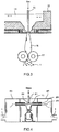
- FIG. 3 shows an example of an apparatus for producing glass flakes by the blow process.
- the production apparatus is equipped with a refractory tank furnace 12, blowing nozzle 15, and pressing rolls 17.
- a glass raw material 11 is melted in the refractory tank furnace 12 (melting furnace) and is inflated into a balloon by a gas delivered through the blowing nozzle 15, so that hollow glass 16 is obtained.
- the hollow glass 16 is crushed by the pressing rolls 17 to obtain a glass flake 1.
- the thickness of the glass flake 1 can be controlled by adjusting, for example, the speed of pulling the hollow glass 16 and flow rate of the gas delivered through the blowing nozzle 15.
- FIG. 4 shows an example of an apparatus for producing glass flakes by the rotary process.
- the apparatus is equipped with a rotary cup 22, pair of annular plates 23, and annular cyclone collector 24.
- a molten glass raw material 11 is poured into the rotary cup 22, centrifugally flows out from the upper edge of the rotary cup 22 in a radial manner, and is then drawn and carried into the annular cyclone collector 24 through the gap between the annular plates 23 by airflow.
- the glass While passing through the annular plates 23, the glass is cooled and solidified into a thin film, which is then crushed into fine pieces to give a glass flake 1.
- the thickness of the glass flake 1 can be controlled by adjusting, for example, the distance between the annular plates 23 and velocity of the airflow.
- the alumina flake is a general-purpose flaky substrate just as the glass flake.
- Alumina composing the alumina flake is preferably ⁇ -alumina (refractive index: 1.76).
- the alumina flake preferably has an average particle diameter of 1 to 1000 ⁇ m, even 3 to 500 ⁇ m, particularly 5 to 200 ⁇ m, and more particularly 10 to 100 ⁇ m.
- the average particle diameter of the alumina flake is determined as a particle diameter (D50) as is the case for the average particle diameter of the glass flake.
- Alumina flakes commonly have a thickness of about 1 ⁇ m or less, and a general-purpose product having a thickness of about 0.8 ⁇ m is also commercially-available.
- the thickness of the alumina flake is set in the very narrow range (260 to 280 nm).
- the alumina flake can be produced by a conventionally known method, for example, a method in which an alkali such as sodium hydroxide or sodium carbonate and a phosphorus compound such as a phosphoric acid or phosphoric acid salt are added to an aqueous solution containing an aluminum salt dissolved to obtain a precipitate containing aluminum hydroxide and the precipitate is heat-treated as appropriate.
- this method may include the following steps.
- Examples of the dopant include titanium oxide, zirconium oxide, and silicon oxide.
- the amount of the dopant added is preferably as small as about 0.05 to 3 weight% with respect to the alumina flake.
- the thickness of the alumina flake can be controlled in the above exemplary method by appropriately adjusting, for example, the concentrations of the compounds such as the aluminum salt, alkali, and phosphorus compound and heat treatment conditions such as the heat treatment temperature. In addition to that, appropriate conditions are set in the step vi) to obtain the alumina flake having a thickness controlled in the desired range.
- the silicon oxide layer and titanium oxide layer are arranged in this order on the flaky substrate.
- Each of these layers is formed to have the above thickness depending on the type of substrate. There is already an established technique for forming these layers, and these layers are easily formed to have the desired thicknesses.
- the silicon oxide layer can be formed by a method including, for example, a deposition step, such as deposition from sodium silicate (liquid glass) or deposition by hydrolysis of tetraalkoxysilane, and a subsequent thermal condensation step.
- a deposition step such as deposition from sodium silicate (liquid glass) or deposition by hydrolysis of tetraalkoxysilane
- a subsequent thermal condensation step e.g., thermal condensation step.
- the titanium oxide layer is preferably composed of rutile-type titanium oxide.
- the anatase type is also known as a crystalline form of titanium oxide.
- anatase-type titanium oxide is highly active as a photocatalyst and may decompose a surrounding organic substance.
- rutile-type titanium oxide having a high refractive index and being in a relatively stable crystalline form is suitable.
- the rutile-type titanium oxide layer can be formed by heating anatase-type titanium oxide to a temperature as high as about 800°C for transformation to rutile-type titanium oxide.
- the rutile-type titanium oxide layer can be formed, with no need for high-temperature heating, by attaching a tin compound to a surface where the titanium oxide layer is to be formed to deposit titanium oxide. The detail of the latter method is disclosed, for example, in Patent Literature 2 and JP 2001-031421 A .
- the glitter pigment according to the present invention exhibits a vivid whitish color when incorporated in various compositions.
- the present invention provides a pigment-containing composition containing the glitter pigment according to the present invention.
- An example of the pigment-containing composition is at least one selected from a paint, ink, cosmetic, and resin composition.
- the resin composition include those containing a resin which is PMMA and/or polycarbonate in addition to the glitter pigment.
- the resin composition may be a molded product of artificial marble.
- the present invention provides a pigment-containing painted product including a substrate material and a paint film formed on the substrate material, the paint film containing the glitter pigment according to the present invention.
- the pigment-containing painted product may be painted paper.
- the substrate material is paper.
- the substrate material is not limited to paper, and may be a metal, resin, ceramic, or another material.
- the paint film may be composed of the pigment-containing composition according to the present invention or may be formed by applying the pigment-containing composition according to the present invention onto the substrate material.
- the optical properties including the reflectance properties can be calculated based on the straightness of light, the law of reflection, and the law of refraction (Snell's law) from the refractive indices (n) and extinction coefficients (k), at a certain wavelength, of the materials of the laminate structure (flaky substrate and layers) and the thicknesses of the flaky substrate and layers. It is well known that the reflectance properties calculated by means of the theory of geometrical optics well correspond to the properties of an actual product.
- a model of the structure used for the calculation is the surrounding (external environment)/TiO 2 /SiO 2 /the flaky substrate (glass flake or alumina flake)/SiO 2 /TiO 2 /the surrounding (external environment). It was assumed that the glass flake was made of soda-lime glass and the alumina flake was made of ⁇ -alumina. The titanium oxide layer was assumed to be made of rutile-type titanium oxide. The surrounding was assumed to air (refractive index: 1.0) or a resin. It was assumed that the resin was a typical transparent resin, polymethylmethacrylate (PMMA; refractive index: 1.49) or polycarbonate (refractive index: 1.59).
- PMMA polymethylmethacrylate
- PMMA polymethylmethacrylate
- polycarbonate reffractive index: 1.59
- R refers to the reflectance (%) at a wavelength of 550 nm
- L*, a*, and b* are based on the L*a*b* color system.
- Tables 1 to 3 also show the results for calculation using flakes of bismuth oxychloride.
- the suitable thicknesses of the glass flake and layers are in the following ranges in order to obtain a reflected light having absolute values of a* and b* of 30 or less and that the L* value (about 68 or more) higher than ever before can be obtained in air by employing the following ranges.
- the suitable thicknesses of the alumina flake and layers are in the following ranges in order to obtain a reflected light having absolute values of a* and b* of 30 or less and that a quite high L* value (about 72 or more) can be obtained in air by employing the following ranges.
- Table 7 shows the results obtained by changing the thickness of the glass flake to 700 nm and the thickness of the silicon oxide layer to 70 nm and calculating in the same manner as above (refer to Examples 1 to 8 of Patent Literature 2). It can be understood that the L* value of reflected light is 67 or less and that the L* value is maximum when the thickness of the titanium oxide layer is 70 to 80 nm.
- Substrate glass; surrounding: air Su bstrate Thickness (nm) Reflectance properties Flake SiO 2 TiO 2 R(%) L* a* b* Glass 700 70 40 24 56 -10 -25 Glass 700 70 50 30 62 -17 -20 Glass 700 70 60 35 66 -19 -13 Glass 700 70 70 37 67 -16 -4 Glass 700 70 80 37 67 -11 6 Glass 700 70 90 35 65 -5 20 Glass 700 70 100 30 62 2 36 Glass 700 70 110 25 57 12 46 [Table 8] Substrate: glass; surrounding: air Substrate Thickness (nm) Reflectance properties Flake SiO 2 TiO 2 R(%) L* a* b* Glass 300 70 10 5 28 10 -8 Glass 300 70 20 7 32 47 -43 Glass 300 70 30 10 38 34 -49 Glass 300 70 40 17 48 -11 -34 Glass 300 70 50 26 58 -53 -11 Glass 300 70 60 35 66 -69 11 Glass 300 70 70 42 71 -62 25 Glass 300 70 80 45
- the L* value is increased but whitish reflected light cannot be produced. Additionally, for the combination of the thicknesses (titanium oxide layer: 10 nm or 180 nm) with which a reflected light having absolute values of a* and b* of 30 or less is produced, the L* value is greatly decreased.
- the layer thicknesses suitable for the use with a thick flaky substrate are employed for a thin flaky substrate, high brightness is achieved for colored reflected light but not for whitish reflected light.
- the thicknesses of the silicon oxide layer and titanium oxide layer are often adjusted by a method in which the titanium oxide layer on the silicon oxide layer having a predetermined thickness is increased in thickness (Table 8) while reflected light is kept under observation.
- this method is capable of adjusting the thickness of the titanium oxide layer appropriately in relation to the thickness of a layer other than the titanium oxide layer, it is difficult to adjust the thickness of each of the layers including the other layer so that the layers will have mutually appropriate thicknesses.
- the properties of a reflected light from one piece of a pigment are calculated in every case of the above optical simulation.
- reflected light from, for example, an actual paint film, where there are a plurality of pieces of a pigment in the transmission direction of light is observed to have higher brightness than the brightness determined by the optical simulation. This is reproduced by the optical simulation, for example, as follows.
- Substrate glass; surrounding: PMMA Substrate Thickness (nm) Reflectance properties Type Number of overlapping pigments Flake SiO 2 TiO 2 R(%) L* a* b* Glass 1 700 70 80 18 49 -9 0 Glass 2 700 70 80 28 60 -10 1 Glass 3 700 70 80 36 66 -10 1 Glass 4 700 70 80 41 70 -11 1 Glass 5 700 70 80 45 73 -11 1 Glass 6 700 70 80 49 75 -11 1
Abstract
Description
- The present invention relates to glitter pigments, particularly relates to a glitter pigment including a glass flake or alumina flake as a substrate, and more particularly relates to a glitter pigment capable of providing high-brightness whitish reflected light. The present invention also relates to a composition containing a glitter pigment and to a painted product having a paint film containing a glitter pigment.
- Particles of, for example, titanium oxide, zinc oxide, cerium oxide, calcium carbonate, and barium sulfate are widely used as whitish pigments. Compared to particulate pigments, flaky pigments are advantageous to increase the brightness of reflected light and improve the gloss of the pigments. Since a principal surface of a flaky pigment is oriented in a paint film along a paint film surface, flaky pigments are suitable for improving the brightness of reflected light, particularly, from a paint film. Moreover, cosmetics containing a flaky pigment spread well when used and such cosmetics are suitable for allowing users to experience a smooth texture.
- As a flaky whitish pigment, a flake of bismuth oxychloride (BiOCl) is known. A flake of bismuth oxychloride can be obtained by hydrolysis of bismuth trichloride. The reflected light from this whitish pigment has relatively high brightness.
Patent Literature 1 proposes addition of an anti-ultraviolet stabilizer such as an organic ultraviolet absorber to a pigment to improve insufficient light resistance of bismuth oxychloride. - However, an additive incorporated to improve the light resistance of bismuth oxychloride causes a further increase in production cost of pigments. A flaky whitish pigment composed not of an oxychloride but of a stable compound. typified by an oxide needs no additives for the improvement in light resistance.
- Patent Literature 2 discloses a whitish pigment produced by forming a silicon oxide layer and titanium oxide layer in this order on a glass flake. According to Examples 1 to 8 of Patent Literature 2, the L* value, which is a measure of the brightness of reflected light, is in the range of 73 to 76 (Table 2). The reflected light of Examples 1 to 8 is a whitish light having a chroma C* value in the range of 2.16 to 3.6. Examples 1 to 8 of Patent Literature 2 describes that the average thickness of the glass flake is 700 nm, that the thickness of the silicon oxide layer is 7 to 70 nm, and additionally that the L* value reaches the highest value when the silicon oxide layer has a thickness of 70 nm (Examples 1 and 2 on Table 3). The thickness of the titanium oxide layer is not disclosed specifically.
-
- Patent Literature 1:
JP 2005-532467 A - Patent Literature 2:
JP 2006-510797 A - For the titanium oxide layers in Examples 1 and 2 of Patent Literature 2, the thickness at which the brightness of the resultant reflected light is maximized can be calculated by optical simulation. According to the optical simulation described later in detail, the titanium oxide layer has a thickness of about 70 to 80 nm when the L* value is maximum. The maximum L* value is about 67 when the pigment is surrounded by air, and the maximum L* value is about 49 when the pigment is surrounded by a resin (polymethylmethacrylate (PMMA)) (refer to Tables 7 and 9 of the present invention). The L* value of reflected light actually measured in Patent Literature 2 is 76, which is beyond the L* value obtained by the calculation. The differences in L* values result from the fact that reflected light from one piece of the pigment is calculated in the optical simulation, while reflected light from a plurality of pigment pieces overlapping in the thickness direction is observed in the case of a coating card (refer to Examples of Patent Literature 2) including the flaky whitish pigment dispersed (refer to Table 9 of the present invention).
- To further increase the brightness of reflected light, it is conceivable to increase the number of layers of an optical interference system composed of two layers, i.e., the titanium oxide layer which is a high refractive index layer and the silicon oxide layer which is a low refractive index layer. Patent Literature 2 also suggests this method (in Paragraph 0032). However, the increase of the number of layers causes an increase in production cost and thickness of the resultant pigment.
- Therefore, the present invention aims to provide a new glitter pigment suitable for providing high-brightness whitish reflected light without increasing the number of layers.
- A study by the present inventors has revealed that the brightness of whitish reflected light can be further improved by using a flaky substrate such as a glass flake as a layer for forming an optical interference system in addition to a silicon oxide layer and titanium oxide layer. That is, in the present invention, a flaky substrate is used not only as a substrate on which a layer is formed, but also as a part of an optical interference system.
- The present invention provides a glitter pigment, including:
- a flaky substrate; and
- a silicon oxide layer and a titanium oxide layer formed in this order on the flaky substrate, wherein
- the silicon oxide layer and the titanium oxide layer are formed on both a first principal surface and a second principal surface of the flaky substrate, the first principal surface and the second principal surface being opposite to each other,
- the flaky substrate is a glass flake or an alumina flake,
- a) in the case where the flaky substrate is the glass flake,
the glass flake has a thickness of 284 nm or more and 322 nm or less,
the silicon oxide layer has a thickness of 89 nm or more and 109 nm or less, and
the titanium oxide layer has a thickness of 51 nm or more and 86 nm or less, - b) in the case where the flaky substrate is the alumina flake,
- a) in the case where the flaky substrate is the glass flake,
- the alumina flake has a thickness of 260 nm or more and 280 nm or less,
- the silicon oxide layer has a thickness of 79 nm or more and 102 nm or less, and
- the titanium oxide layer has a thickness of 47 nm or more and 87 nm or less, and
- whitish reflected light is produced by a five-layer optical interference system composed of the titanium oxide layer, the silicon oxide layer, the flaky substrate, the silicon oxide layer, and the titanium oxide layer which are arranged in this order along a thickness direction of the flaky substrate.
- The term "optical interference system" as used herein refers to a layer unit formed by continuously stacking, in the thickness direction, layers having an optical thickness of 780 nm, which is the upper end of the visible wavelength range, or less. However, a thin layer having a thickness of 25 nm or less, particularly a very thin layer having a thickness of 15 nm or less, and a small matter attaching like an island and not forming a layer are not counted as a layer for forming the optical interference system because of their very limited optical influence. Thus, even when a thin layer having a thickness of the above-described upper end value or less intervenes between the layers of the above optical interference system, the optical interference system remains to have a five-layer structure. Generally, the more the number of layers composing the optical interference system increases, the more flexible the optical design becomes for controlling the transmission in the visible range or the reflectance properties.
- Additionally, the term "whitish" as used herein refers to being a color whose absolute values of a* and b* are both 30 or less, preferably 25 or less, more preferably 20 or less, and particularly preferably 15 or less, in the L*a*b* color system. The term "thickness" refers to the physical thickness instead of the optical thickness, unless otherwise specified.
- The present invention provides a whitish glitter pigment including an oxide with excellent light resistance and suitable for providing high-brightness reflected light. The thickness of each layer of the five-layer optical interference system according to the present invention is adjusted so that high-brightness reflected light is produced not only when the five-layer optical interference system exists alone as a product, i.e., when the five-layer optical interference system is surrounded by air, but also when the five-layer optical interference system is dispersed in a typical resin.
-
-
FIG. 1 is a cross-sectional view illustrating the structure of a glitter pigment according to an embodiment of the present invention. -
FIG. 2 is a perspective view illustrating a flaky substrate according to an embodiment. -
FIG. 3 is a schematic diagram illustrating an exemplary apparatus for producing glass flakes. -
FIG. 4 is a schematic diagram illustrating another exemplary apparatus for producing glass flakes. - Hereinafter, the present invention will be described in detail. The following description is not intended to limit the present invention to specific embodiments.
- In the embodiment shown in
FIG. 1 , aglitter pigment 10 includes: aflaky substrate 1; and a silicon oxide layer 2 and atitanium oxide layer 3 formed in this order on theflaky substrate 1. More specifically, the silicon oxide layer 2 and thetitanium oxide layer 3 are formed on both a firstprincipal surface 1a and a secondprincipal surface 1b of theflaky substrate 1, the firstprincipal surface 1a and the secondprincipal surface 1b being opposite to each other, and also formed on aside surface 1s. In other words, an oxide film composed of the silicon oxide layer 2 andtitanium oxide layer 3 covers the entireflaky substrate 1. Thetitanium oxide layer 3 is the outermost layer of the oxide film covering theflaky substrate 1 and has contact with the external atmosphere, typically, air. On thetitanium oxide layer 3, however, theglitter pigment 10 may have an additional layer having an optical thickness beyond the visible wavelengths. The additional layer is, for example, a protective layer. The firstprincipal surface 1a and secondprincipal surface 1b are a pair of surfaces substantially parallel to each other, and the distance therebetween corresponds to the thickness t of theflaky substrate 1. -
FIG. 2 shows a typical shape of theflaky substrate 1. As shown inFIG. 2 , theflaky substrate 1 is, for example, a scale-like thin piece. - The
glitter pigment 10 has thetitanium oxide layer 3, silicon oxide layer 2,flaky substrate 1, silicon oxide layer 2, andtitanium oxide layer 3 as an optical interference system along the direction of the thickness t of theflaky substrate 1. Theflaky substrate 1 is a glass flake or alumina flake. - In the case where the flaky substrate is the glass flake, the thickness of each layer of the optical interference system is adjusted as follows. In the round brackets are the ranges suitable for making the absolute values of a* and b* of reflected light smaller and the L* value of reflected light greater.
- Glass flake: 284 to 322 nm (294 to 314 nm)
- Silicon oxide layer: 89 to 109 nm (92 to 102 nm)
- Titanium oxide layer: 51 to 86 nm (56 to 76 nm)
- It is recommended that the thickness of each layer of the glitter pigment to be dispersed in a resin be adjusted depending on the type of resin. When the resin is, for example, PMMA (polymethylmethacrylate) or polycarbonate, the preferable thickness ranges are as follows.
-
- Glass flake: 287 to 312 nm
- Silicon oxide layer: 94 to 109 nm
- Titanium oxide layer: 52 to 86 nm
-
- Glass flake: 286 to 306 nm
- Silicon oxide layer: 94 to 104 nm
- Titanium oxide layer: 56.5 to 86 nm
- The two ranges defined for each layer overlap as follows.
- Glass flake: 287 to 306 nm
- Silicon oxide layer: 94 to 104 nm
- Titanium oxide layer: 56.5 to 86 nm
- In the case where the flaky substrate is the alumina flake, the thickness (physical thickness) of each layer of the optical interference system is adjusted as follows. In the round brackets are the ranges suitable for making the absolute values of a* and b* of reflected light smaller and the L* value of reflected light greater.
- Alumina flake: 260 to 280 nm (265 to 280 nm)
- Silicon oxide layer: 79 to 102 nm (83 to 98 nm)
- Titanium oxide layer: 47 to 87 nm (51.5 to 71.5 nm)
- In the case of the alumina flake as well, it is recommended that the thickness of each layer of the glitter pigment to be dispersed in a transparent resin be adjusted depending on the type of transparent resin. When the transparent resin is PMMA or polycarbonate, the preferable thickness ranges are as follows.
-
- Alumina flake: 260 to 275 nm
- Silicon oxide layer: 79 to 102 nm
- Titanium oxide layer: 47 to 84 nm
-
- Alumina flake: 260 to 278 nm
- Silicon oxide layer: 79 to 97 nm
- Titanium oxide layer: 47 to 82 nm
- The two ranges defined for each layer overlap as follows.
- Alumina flake: 260 to 275 nm
- Silicon oxide layer: 79 to 97 nm
- Titanium oxide layer: 47 to 82 nm
- It should be noted that the thickness of each layer is not limited to the above, and can be adjusted so that both of the absolute values of a* and b* of reflected light will be a predetermined value or less, namely, 30 or less, for example, 15 or less.
- A conventional pigment causing whitish reflected light is composed of a substrate alone or has a structure including two optical interference systems respectively arranged on opposite sides of a flaky pigment (refer to Examples 1 to 8 of Patent Literature 2). Meanwhile, in the
glitter pigment 10, thelayers 2 and 3 forming a two-layer film and theflaky substrate 1 form a five-layer optical interference system as a whole. Because of reflection from each layer of this five-layer optical interference system, theglitter pigment 10 provides whitish reflected light. More specifically, light L incident on the firstprincipal surface 1a or secondprincipal surface 1b from a substantially vertical direction produces whitish reflected light (whose absolute values of a* and b* in L*a*b* color system are both 30 or less, as described previously). Although the number of layers formed is two, the five-layer optical interference system can be used. Theglitter pigment 10, therefore, is more advantageous for producing high-bright whitish reflected light in terms of optical design than a pigment including a two-layer optical interference system on each surface of its substrate. - According to optical simulation, the glitter pigment according to the present embodiment having the five-layer optical interference system, in which, for example, the silicon oxide layer having a thickness of 97 nm and titanium oxide layer having a thickness of 65.9 nm are sequentially arranged to cover the surfaces of the glass flake having a thickness of 300 nm, produces a whitish reflected light (a*: -4; b*: 6) having an L* value of 74 (when surrounded by air; the same applies to the present and next paragraphs). When the above thicknesses of the silicon oxide layer and titanium oxide layer are maintained and the thickness of the glass flake is increased beyond the above suitable range (284 to 322 nm), the resultant pigment can also produce a whitish reflected light, whose L* value is less than 74. Generally, when the optical thickness of the glass flake is sufficiently greater than the visible wavelengths, the brightness and color of the resultant reflected light is less likely to be affected by a change in thickness of the glass flake. For example, when the silicon oxide layer and titanium oxide layer have the above thicknesses and the glass flake has a thickness in the range of 1000 nm to 5000 nm, the resultant pigment produces a whitish reflected light having a brightness value within a narrow range, namely, 61 to 67. Just by increasing the thickness of the glass flake alone from 300 nm to 400 nm and keeping the above thicknesses of the silicon oxide layer and titanium oxide layer, the L* value of the reflected light of the resultant glitter pigment decreases from 74 to 63. Moreover, just by decreasing the thickness of the glass flake alone from 300 nm to 200 nm, the L* value of the reflected light of the resultant glitter pigment decreases from 74 to 55, and the reflected light is colored and not whitish. When the flaky substrate is so thin that the optical thickness thereof is within the range corresponding to wavelengths in or below the visible range, a change in thickness of the flaky substrate causes a great change in brightness and color of the resultant reflected light. However, proper control of the thickness of each layer of the structure, namely, the five-layer optical interference system, including such a thin flaky substrate can increase the brightness of a whitish reflected light.
- The physical thickness of a glass flake having an optical thickness of 780 nm, which is the upper end of the visible wavelength range, or less is about 500 nm or less. The physical thickness of an alumina flake having an optical thickness of 780 nm or less is about 450 nm or less. General-purpose flaky substrates have a thickness of 500 nm or more. Glass flakes and alumina flakes having a thickness of about less than 500 nm are also known. However, an optical interference system including a thin flaky substrate is conventionally used to obtain colored reflected light instead of whitish reflected light.
- In Examples 21 and 22 of Patent Literature 2, for example, silicon oxide layers are formed on a glass flake having an average thickness of 500 nm. The silicon oxide layers are 10% with respect to the glass, i.e., each of the silicon oxide layers has a thickness of 25 nm (the total thickness of the silicon oxide layers each arranged on either principal surface of the glass is 50 nm). An iron oxide layer (Example 21) or titanium oxide layer (Example 22) is formed on each of the silicon oxide layers. An iron oxide red pigment is obtained in Example 21, and a pigment presenting a bright interference color having a predetermined hue angle, namely, a pigment presenting a colored light is obtained in Example 22. It is also confirmed in Example 11 of Patent Literature 2 that "higher chroma (tinting strength)" is achieved with the use of an about 200-nm-thick alumina flake. As is apparent from these Examples, basically an optical interference system employing about five- or more-layer laminate structure has conventionally been designed to provide a reflected light having a great chroma C* value, namely, colored reflected light. On the other hand, the optical interference system according to the present embodiment provides a whitish reflected light having a small chroma C* value.
- From the amount of the raw materials used, the thickness of the silicon oxide layer of Example 22 of Patent Literature 2 is calculated to be about 35 to 45 nm. Even if the thickness of the titanium oxide layer was optimized to obtain whitish reflected light in Example 22, the brightness of the whitish reflected light would not be increased sufficiently (according to the optical simulation, a pigment in which the titanium oxide layer has a thickness of about 60 to 70 nm and which is surrounded by air produces a reflected light having an L* value of only 58 or so). In Example 22, the maximum L* value obtainable by adjusting the thickness of the titanium oxide layer is achieved by a colored reflected light (a slightly yellowish green reflected light having an L* value of about 62 to 65 can be obtained when the thickness of the titanium oxide layer is 90 nm).
- With the use of the five-layer optical interference system according to the present embodiment, the L* value of the whitish reflected light from the pigment in the L*a*b* color system, as calculated by the optical simulation, can be increased to, for example, 68 or more, preferably 70 or more, more preferably 71 or more, even more preferably 72 or more, and particularly preferably 73 or more. This L* value is of a reflected light from one piece of the pigment. An actual paint film containing a plurality of pieces of the pigment reflecting light, for example, may produce a reflected light whose L* value is greater than the above values and is, for example, 80 or more, even 82 or more, and particularly about 85 or more. The L* value described in this paragraph refers to a value obtained when the glitter pigment exists alone, in other words, when the glitter pigment is not surrounded by a solid or liquid matrix of a paint film or the like and the surrounding atmosphere is air.
- With the use of the five-layer optical interference system according to the present embodiment, the reflectance R of one piece of the pigment at a wavelength of 550 nm, as calculated by the optical simulation, can be increased to 40% or more, even 42% or more, particularly 44% or more, and in some cases 46% or more. Here, the "wavelength of 550 nm" is selected as a wavelength at which the visual sensitivity is high. This paragraph describes the reflectance R obtained also when the glitter pigment exists alone, in other words, when the glitter pigment is not surrounded by a matrix of a paint film or the like and the surrounding atmosphere is air.
- The thickness of each layer of the five-layer optical interference system according to the present embodiment is designed in consideration of not only the case where the surrounding atmosphere is air but also the case where the surrounding is a resin, namely, the case where the optical interference system is dispersed in a paint film. The five-layer optical interference system according to the present embodiment, therefore, has great versatility.
- The flaky substrate is a glass flake or alumina flake. These flaky substrates are mass-produced and thus easily available, and composed of an oxide material which is stable.
- The glass flake is a fine, plate-like glass substrate which can be called, for example, a scaly glass particle. The glass composition for forming the glass flake is not particularly limited. A glass composition containing silicon dioxide as a main component and further containing other metal oxides such as aluminum oxide, calcium oxide, and sodium oxide is typically used. The term "main component" is used herein to refer to a component whose content is highest in terms of mass. Examples of glass compositions that can be used include soda-lime glass, A-glass, C-glass, E-glass, borosilicate glass, and aluminosilicate glass. The refractive indices of these glass compositions, which have the same main component (silicon dioxide), are roughly in the range of 1.50 to 1.60, albeit differing slightly. As the glass composition, soda-lime glass, C-glass, E-glass, and borosilicate glass are preferred, and the refractive indices thereof are in the range of 1.52 to 1.58.
- The glass flake preferably has an average particle diameter of 1 to 1000 µm, even 3 to 500 µm, and particularly 5 to 200 µm. The average particle diameter of the glass flake is determined as a particle diameter (D50) at 50% by volume in a cumulative undersize distribution of light scattering-based particle sizes measured by laser diffractometry.
- General-purpose products of glass flakes have a thickness of about 0.4 to 5 µm. However, to obtain high-bright whitish reflected light by the combination with the laminate film composed of the silicon oxide layer and titanium oxide layer, the thickness of the glass flake is set in the very narrow range (284 to 322 nm) described above. Glass flakes having a thickness in this range can be produced by a conventionally known method, for example, a blow process and rotary process.
-
FIG. 3 shows an example of an apparatus for producing glass flakes by the blow process. The production apparatus is equipped with arefractory tank furnace 12, blowingnozzle 15, and pressing rolls 17. A glassraw material 11 is melted in the refractory tank furnace 12 (melting furnace) and is inflated into a balloon by a gas delivered through the blowingnozzle 15, so thathollow glass 16 is obtained. Thehollow glass 16 is crushed by the pressing rolls 17 to obtain aglass flake 1. The thickness of theglass flake 1 can be controlled by adjusting, for example, the speed of pulling thehollow glass 16 and flow rate of the gas delivered through the blowingnozzle 15. -
FIG. 4 shows an example of an apparatus for producing glass flakes by the rotary process. The apparatus is equipped with arotary cup 22, pair ofannular plates 23, andannular cyclone collector 24. A molten glassraw material 11 is poured into therotary cup 22, centrifugally flows out from the upper edge of therotary cup 22 in a radial manner, and is then drawn and carried into theannular cyclone collector 24 through the gap between theannular plates 23 by airflow. While passing through theannular plates 23, the glass is cooled and solidified into a thin film, which is then crushed into fine pieces to give aglass flake 1. The thickness of theglass flake 1 can be controlled by adjusting, for example, the distance between theannular plates 23 and velocity of the airflow. - The alumina flake is a general-purpose flaky substrate just as the glass flake. Alumina composing the alumina flake is preferably α-alumina (refractive index: 1.76).
- The alumina flake preferably has an average particle diameter of 1 to 1000 µm, even 3 to 500 µm, particularly 5 to 200 µm, and more particularly 10 to 100 µm. The average particle diameter of the alumina flake is determined as a particle diameter (D50) as is the case for the average particle diameter of the glass flake.
- Alumina flakes commonly have a thickness of about 1 µm or less, and a general-purpose product having a thickness of about 0.8 µm is also commercially-available. However, to obtain high-bright whitish reflected light by the combination with the laminate film composed of the silicon oxide layer and titanium oxide layer, the thickness of the alumina flake is set in the very narrow range (260 to 280 nm). The alumina flake can be produced by a conventionally known method, for example, a method in which an alkali such as sodium hydroxide or sodium carbonate and a phosphorus compound such as a phosphoric acid or phosphoric acid salt are added to an aqueous solution containing an aluminum salt dissolved to obtain a precipitate containing aluminum hydroxide and the precipitate is heat-treated as appropriate. Specifically, this method may include the following steps.
-
- i) A step of adding an alkali to an aqueous solution containing an aluminum salt dissolved or a slurry containing an aluminum salt to form a precipitate containing aluminum hydroxide.
- ii) A step of adding a phosphorus compound and, if necessary, a dopant to the aqueous solution, slurry, or precipitate before or after the step i) or during the formation of the precipitate in the step i).
- iii) A step of drying the precipitate after the steps i) and ii) to obtain a dry matter.
- iv) A step of subjecting the dry matter to heat treatment, for example, at 900 to 1400°C for 0.5 to 10 hours to obtain an alumina flake in a molten salt.
- v) A step of removing a water-soluble part of the product of the heat treatment, for example, by washing with water.
- vi) A step of adjusting the average particle diameter and thickness of the alumina flake by appropriately combining, for example, sieving, crushing, and sedimentation.
- Examples of the dopant include titanium oxide, zirconium oxide, and silicon oxide. The amount of the dopant added is preferably as small as about 0.05 to 3 weight% with respect to the alumina flake.
- The thickness of the alumina flake can be controlled in the above exemplary method by appropriately adjusting, for example, the concentrations of the compounds such as the aluminum salt, alkali, and phosphorus compound and heat treatment conditions such as the heat treatment temperature. In addition to that, appropriate conditions are set in the step vi) to obtain the alumina flake having a thickness controlled in the desired range.
- The silicon oxide layer and titanium oxide layer are arranged in this order on the flaky substrate. Each of these layers is formed to have the above thickness depending on the type of substrate. There is already an established technique for forming these layers, and these layers are easily formed to have the desired thicknesses.
- The silicon oxide layer can be formed by a method including, for example, a deposition step, such as deposition from sodium silicate (liquid glass) or deposition by hydrolysis of tetraalkoxysilane, and a subsequent thermal condensation step. The detail of this method is disclosed, for example, in Patent Literature 2.
- The titanium oxide layer is preferably composed of rutile-type titanium oxide. The anatase type is also known as a crystalline form of titanium oxide. However, anatase-type titanium oxide is highly active as a photocatalyst and may decompose a surrounding organic substance. For the titanium oxide layer for forming the optical interference unit, rutile-type titanium oxide having a high refractive index and being in a relatively stable crystalline form is suitable.
- The rutile-type titanium oxide layer can be formed by heating anatase-type titanium oxide to a temperature as high as about 800°C for transformation to rutile-type titanium oxide. Alternatively, the rutile-type titanium oxide layer can be formed, with no need for high-temperature heating, by attaching a tin compound to a surface where the titanium oxide layer is to be formed to deposit titanium oxide. The detail of the latter method is disclosed, for example, in Patent Literature 2 and
JP 2001-031421 A - The glitter pigment according to the present invention exhibits a vivid whitish color when incorporated in various compositions. In another aspect, the present invention provides a pigment-containing composition containing the glitter pigment according to the present invention. An example of the pigment-containing composition is at least one selected from a paint, ink, cosmetic, and resin composition. Examples of the resin composition include those containing a resin which is PMMA and/or polycarbonate in addition to the glitter pigment. The resin composition may be a molded product of artificial marble.
- In still another aspect, the present invention provides a pigment-containing painted product including a substrate material and a paint film formed on the substrate material, the paint film containing the glitter pigment according to the present invention. The pigment-containing painted product may be painted paper. In this case, the substrate material is paper. The substrate material is not limited to paper, and may be a metal, resin, ceramic, or another material. The paint film may be composed of the pigment-containing composition according to the present invention or may be formed by applying the pigment-containing composition according to the present invention onto the substrate material.
- The relationship between the thickness of the substrate and layers and the reflectance properties was calculated for pigments each including a silicon oxide layer and titanium oxide layer formed in this order on a flaky substrate to form an optical interference system together with the flaky substrate. As is well known, the optical properties including the reflectance properties can be calculated based on the straightness of light, the law of reflection, and the law of refraction (Snell's law) from the refractive indices (n) and extinction coefficients (k), at a certain wavelength, of the materials of the laminate structure (flaky substrate and layers) and the thicknesses of the flaky substrate and layers. It is well known that the reflectance properties calculated by means of the theory of geometrical optics well correspond to the properties of an actual product.
- A model of the structure used for the calculation is the surrounding (external environment)/TiO2/SiO2/the flaky substrate (glass flake or alumina flake)/SiO2/TiO2/the surrounding (external environment). It was assumed that the glass flake was made of soda-lime glass and the alumina flake was made of α-alumina. The titanium oxide layer was assumed to be made of rutile-type titanium oxide. The surrounding was assumed to air (refractive index: 1.0) or a resin. It was assumed that the resin was a typical transparent resin, polymethylmethacrylate (PMMA; refractive index: 1.49) or polycarbonate (refractive index: 1.59). It was assumed that the light source was illuminant D65, the incident angle of light was 5°, and the location of measurement of reflected light was in a direction of a reflection angle of 5°. The following tables show the results for the calculation of the reflectance properties. R refers to the reflectance (%) at a wavelength of 550 nm, and the values of L*, a*, and b* are based on the L*a*b* color system. Tables 1 to 3 also show the results for calculation using flakes of bismuth oxychloride.
[Table 1] Substrate: glass; surrounding: air Substrate Thickness (nm) Reflectance properties Flake SiO2 TiO2 R(%) L* a* b* BiOCl 100 0 0 24 56 -4 39 BiOCl 200 0 0 26 58 -31 12 BiOCl 300 0 0 10 37 8 -35 Glass 274.0 97.0 65.9 46 74 -45 26 Glass 284.0 97.0 65.9 47 74 -29 19 Glass 294.0 97.0 65.9 47 74 -13 11 Glass 304.0 97.0 65.9 46 74 0 3 Glass 314.0 97.0 65.9 44 72 14 -5 Glass 324.0 97.0 65.9 41 70 26 -11 Glass 334.0 97.0 65.9 38 68 34 -16 Glass 344.0 97.0 65.9 35 66 38 -19 Glass 354.0 97.0 65.9 32 63 38 -19 Glass 304.0 77.0 65.9 44 72 -49 22 Glass 304.0 87.0 65.9 47 74 -23 14 Glass 304.0 92.0 65.9 47 74 -10 8 Glass 304.0 94.5 65.9 47 74 -4 6 Glass 304.0 99.5 65.9 46 78 -7 0 Glass 304.0 102.0 65.9 44 73 12 -2 Glass 304.0 107.0 65.9 43 71 21 -6 Glass 304.0 112.0 65.9 40 70 29 -10 Glass 304.0 117.0 65.9 37 68 34 -11 Glass 304.0 97.0 45.9 38 68 -41 12 Glass 304.0 97.0 50.9 42 71 -30 10 Glass 304.0 97.0 55.9 44 72 -18 7 Glass 304.0 97.0 60.9 46 73 -8 5 Glass 304.0 97.0 63.4 46 74 -3 4 Glass 304.0 97.0 68.4 46 73 6 2 Glass 304.0 97.0 70.9 45 73 10 2 Glass 304.0 97.0 75.9 44 72 17 2 Glass 304.0 97.0 80.9 41 70 23 4 Glass 304.0 97.0 85.9 38 68 27 9 Glass 304.0 97.0 90.9 34 65 31 15 [Table 2] Substrate: glass; surrounding: PMMA Substrate Thickness (nm) Reflectance properties Flake SiO2 TiO2 R(%) L* a* b* BiOCl 100 0 0 4 23 -3 21 BiOCl 200 0 0 5 25 -21 5 BiOCl 300 0 0 2 13 6 -25 Glass 277.0 99.0 67.1 25 57 -31 27 Glass 282.0 99.0 67.1 25 57 -23 23 Glass 287.0 99.0 67.1 25 57 -16 19 Glass 292.0 99.0 67.1 24 56 -8 14 Glass 297.0 99.0 67.1 24 56 -1 9 Glass 302.0 99.0 67.1 23 55 6 4 Glass 307.0 99.0 67.1 22 54 13 -1 Glass 312.0 99.0 67.1 21 53 19 -6 Glass 317.0 99.0 67.1 20 52 24 -10 Glass 322.0 99.0 67.1 19 51 29 -14 Glass 327.0 99.0 67.1 18 50 34 -17 Glass 297.0 84.0 67.1 24 56 -35 25 Glass 297.0 89.0 67.1 25 57 -24 21 Glass 297.0 94.0 67.1 24 57 -12 15 Glass 297.0 104.0 67.1 23 55 9 3 Glass 297.0 109.0 67.1 21 53 19 -3 Glass 297.0 114.0 67.1 20 51 26 -7 Glass 297.0 119.0 67.1 18 49 32 -11 Glass 297.0 99.0 32.1 12 41 7 -11 Glass 297.0 99.0 42.1 16 46 16 -15 Glass 297.0 99.0 47.1 17 48 20 -17 Glass 297.0 99.0 52.1 22 54 -18 11 Glass 297.0 99.0 57.1 23 55 -12 10 Glass 297.0 99.0 62.1 24 56 -6 9 Glass 297.0 99.0 72.1 24 56 4 9 Glass 297.0 99.0 77.1 23 55 8 11 Glass 297.0 99.0 82.1 22 54 12 14 Glass 297.0 99.0 87.1 20 52 16 18 Glass 297.0 99.0 92.1 13 42 -12 -1 Glass 297.0 99.0 97.1 11 40 36 8 [Table 3] Substrate: glass; surrounding: polycarbonate Substrate Thickness (nm) Reflectance properties Flake SiO2 TiO2 R(%) L* a* b* BiOCl 100 0 0 3 19 -3 19 BiOCl 200 0 0 3 20 -19 4 BiOCl 300 0 0 1 10 5 -22 Glass 270.7 94.0 67.5 16 47 -34 22 Glass 275.7 94.0 67.5 16 47 -27 19 Glass 285.7 94.0 67.5 16 47 -14 12 Glass 295.7 94.0 67.5 15 46 -1 3 Glass 305.7 94.0 67.5 14 45 12 -5 Glass 315.7 94.0 67.5 13 43 22 -12 Glass 325.7 94.0 67.5 12 41 30 -17 Glass 330.7 94.0 67.5 11 40 32 -19 Glass 295.7 97.1 67.5 15 46 -36 21 Glass 295.7 84.0 67.5 16 47 -24 16 Glass 295.7 94.0 67.5 15 46 -1 3 Glass 295.7 104.0 67.5 13 43 19 -8 Glass 295.7 109.0 67.5 12 42 26 -12 Glass 295.7 114.0 67.5 11 40 31 -15 Glass 295.7 94.0 36.5 9 36 -31 10 Glass 295.7 94.0 41.5 11 39 -27 9 Glass 295.7 94.0 46.5 12 42 -23 7 Glass 295.7 94.0 56.5 14 45 -12 5 Glass 295.7 94.0 66.5 15 46 -2 3 Glass 295.7 94.0 76.5 15 45 7 5 Glass 295.7 94.0 86.5 13 42 14 12 Glass 295.7 94.0 96.5 10 38 20 22 Glass 295.7 94.0 101.5 9 36 22 28 Glass 295.7 94.0 106.5 7 33 25 34 - It can be confirmed from Tables 1 to 3 that, regardless of whether the surrounding is air or either of the transparent resins, the suitable thicknesses of the glass flake and layers are in the following ranges in order to obtain a reflected light having absolute values of a* and b* of 30 or less and that the L* value (about 68 or more) higher than ever before can be obtained in air by employing the following ranges.
- Glass flake: 284 nm or more and 322 nm or less
- Thickness of silicon oxide layer: 89 nm or more and 109 nm or less
- Thickness of Titanium oxide layer: 51 nm or more and 86 nm or less
- It can be confirmed from Tables 4 to 6 that, regardless of whether the surrounding is air or either of the transparent resins, the suitable thicknesses of the alumina flake and layers are in the following ranges in order to obtain a reflected light having absolute values of a* and b* of 30 or less and that a quite high L* value (about 72 or more) can be obtained in air by employing the following ranges.
- Alumina flake: 260 nm or more and 280 nm or less
- Silicon oxide layer: 79 nm or more and 102 nm or less
- Titanium oxide layer: 47 nm or more and 87 nm or less
- Table 7 shows the results obtained by changing the thickness of the glass flake to 700 nm and the thickness of the silicon oxide layer to 70 nm and calculating in the same manner as above (refer to Examples 1 to 8 of Patent Literature 2). It can be understood that the L* value of reflected light is 67 or less and that the L* value is maximum when the thickness of the titanium oxide layer is 70 to 80 nm.
[Table 7] Substrate: glass; surrounding: air Su bstrate Thickness (nm) Reflectance properties Flake SiO2 TiO2 R(%) L* a* b* Glass 700 70 40 24 56 -10 -25 Glass 700 70 50 30 62 -17 -20 Glass 700 70 60 35 66 -19 -13 Glass 700 70 70 37 67 -16 -4 Glass 700 70 80 37 67 -11 6 Glass 700 70 90 35 65 -5 20 Glass 700 70 100 30 62 2 36 Glass 700 70 110 25 57 12 46 [Table 8] Substrate: glass; surrounding: air Substrate Thickness (nm) Reflectance properties Flake SiO2 TiO2 R(%) L* a* b* Glass 300 70 10 5 28 10 -8 Glass 300 70 20 7 32 47 -43 Glass 300 70 30 10 38 34 -49 Glass 300 70 40 17 48 -11 -34 Glass 300 70 50 26 58 -53 -11 Glass 300 70 60 35 66 -69 11 Glass 300 70 70 42 71 -62 25 Glass 300 70 80 45 73 -43 31 Glass 300 70 90 44 72 -23 35 Glass 300 70 100 39 68 -4 43 Glass 300 70 110 30 62 16 49 Glass 300 70 120 21 53 37 30 Glass 300 70 130 13 43 56 -10 Glass 300 70 140 8 35 63 -42 Glass 300 70 150 7 32 48 -56 Glass 300 70 160 8 35 15 -52 Glass 300 70 170 12 42 -17 -37 Glass 300 70 180 15 46 -28 -28 Glass 300 70 190 24 56 -55 0 Glass 300 70 200 30 61 -64 17 - As shown in Table 8, when the preferable combination of the thicknesses (70 nm and 70 to 80 nm; refer to Table 7) of the silicon oxide layer and titanium oxide layer is employed for a thin glass flake, the L* value is increased but whitish reflected light cannot be produced. Additionally, for the combination of the thicknesses (titanium oxide layer: 10 nm or 180 nm) with which a reflected light having absolute values of a* and b* of 30 or less is produced, the L* value is greatly decreased. When the layer thicknesses suitable for the use with a thick flaky substrate are employed for a thin flaky substrate, high brightness is achieved for colored reflected light but not for whitish reflected light. As can be understood from Patent Literature 2, conventionally, the thicknesses of the silicon oxide layer and titanium oxide layer are often adjusted by a method in which the titanium oxide layer on the silicon oxide layer having a predetermined thickness is increased in thickness (Table 8) while reflected light is kept under observation. Although this method is capable of adjusting the thickness of the titanium oxide layer appropriately in relation to the thickness of a layer other than the titanium oxide layer, it is difficult to adjust the thickness of each of the layers including the other layer so that the layers will have mutually appropriate thicknesses.
- The properties of a reflected light from one piece of a pigment are calculated in every case of the above optical simulation. However, reflected light from, for example, an actual paint film, where there are a plurality of pieces of a pigment in the transmission direction of light, is observed to have higher brightness than the brightness determined by the optical simulation. This is reproduced by the optical simulation, for example, as follows.
[Table 9] Substrate: glass; surrounding: PMMA Substrate Thickness (nm) Reflectance properties Type Number of overlapping pigments Flake SiO2 TiO2 R(%) L* a* b* Glass 1 700 70 80 18 49 -9 0 Glass 2 700 70 80 28 60 -10 1 Glass 3 700 70 80 36 66 -10 1 Glass 4 700 70 80 41 70 -11 1 Glass 5 700 70 80 45 73 -11 1 Glass 6 700 70 80 49 75 -11 1 - In a paint film, it is common to observe reflected light from three to six pieces of a pigment. The L* values obtained by the optical simulation are approximately equal to the L* value (76) of the reflected light measured in Examples 1 and 2 of Patent Literature 2.
| Substrate: alumina; surrounding: air | |||||||
| Su bstrate | Thickness (nm) | Reflectance properties | |||||
| Flake | SiO2 | TiO2 | R(%) | L* | a* | b* | |
| Alumina | 255.0 | 88.0 | 61.5 | 54 | 78 | -36 | 26 |
| Alumina | 260.0 | 88.0 | 61.5 | 54 | 79 | -27 | 21 |
| Alumina | 265.0 | 88.0 | 61.5 | 54 | 78 | -18 | 16 |
| Alumina | 270.0 | 88.0 | 61.5 | 53 | 78 | -9 | 10 |
| Alumina | 275.0 | 88.0 | 61.5 | 52 | 77 | 1 | 3 |
| Alumina | 280.0 | 88.0 | 61.5 | 51 | 76 | 8 | -2 |
| Alumina | 285.0 | 88.0 | 61.5 | 49 | 75 | 16 | -7 |
| Alumina | 295.0 | 88.0 | 61.5 | 44 | 72 | 30 | -17 |
| Alumina | 300.0 | 88.0 | 61.5 | 42 | 71 | 35 | -21 |
| Alumina | 275.0 | 73.0 | 61.5 | 50 | 76 | -341 | 18 |
| Alumina | 275.0 | 78.0 | 61.5 | 51 | 77 | -22 | 14 |
| Alumina | 275.0 | 83.0 | 61.5 | 52 | 77 | -11 | 9 |
| Alumina | 275.0 | 93.0 | 61.5 | 51 | 77 | 10 | -1 |
| Alumina | 275.0 | 98.0 | 61.5 | 50 | 76 | 18 | -5 |
| Alumina | 275.0 | 103.0 | 61.5 | 48 | 75 | 26 | -9 |
| Alumina | 275.0 | 108.0 | 61.5 | 45 | 73 | 32 | -11 |
| Alumina | 275.0 | 88.0 | 41.5 | 40 | 69 | -39 | 12 |
| Alumina | 275.0 | 88.0 | 46.5 | 45 | 73 | -29 | 11 |
| Alumina | 275.0 | 88.0 | 51.5 | 48 | 75 | -18 | 8 |
| Alumina | 275.0 | 88.0 | 56.5 | 51 | 77 | -9 | 6 |
| Alumina | 275.0 | 88.0 | 66.5 | 52 | 77 | 8 | 2 |
| Alumina | 275.0 | 88.0 | 71.5 | 52 | 77 | 15 | 1 |
| Alumina | 275.0 | 88.0 | 81.5 | 47 | 74 | 26 | 4 |
| Alumina | 275.0 | 88.0 | 86.5 | 44 | 72 | 30 | 8 |
| Alumina | 275.0 | 88.0 | 91.5 | 40 | 70 | 32 | 14 |
| Substrate: alumina; surrounding: PMMA | |||||||
| Substrate | Thickness (nm) | Reflectance properties | |||||
| Flake | SiO2 | TiO2 | R(%) | L* | a* | b* | |
| Alumina | 250.0 | 94.0 | 64.0 | 35 | 66 | -24 | 33 |
| Alumina | 255.0 | 94.0 | 64.0 | 34 | 65 | -15 | 27 |
| Alumina | 260.0 | 94.0 | 64.0 | 33 | 64 | -6 | 19 |
| Alumina | 262.5 | 94.0 | 64.0 | 33 | 64 | -2 | -16 |
| Alumina | 265.0 | 94.0 | 64.0 | 32 | 63 | 3 | 12 |
| Alumina | 270.0 | 94.0 | 64.0 | 31 | 62 | 11 | 4 |
| Alumina | 275.0 | 94.0 | 64.0 | 29 | 61 | 20 | -3 |
| Alumina | 280.0 | 94.0 | 64.0 | 27 | 59 | 27 | -10 |
| Alumina | 285.0 | 94.0 | 64.0 | 25 | 57 | 34 | -16 |
| Alumina | 265.0 | 74.0 | 64.0 | 31 | 62 | -36 | 29 |
| Alumina | 265.0 | 79.0 | 64.0 | 32 | 63 | -26 | 27 |
| Alumina | 265.0 | 84.0 | 64.0 | 33 | 64 | -16 | 23 |
| Alumina | 265.0 | 89.0 | 64.0 | 33 | 64 | -7 | 17 |
| Alumina | 265.0 | 99.0 | 64.0 | 31 | 62 | 11 | 7 |
| Alumina | 265.0 | 104.0 | 64.0 | 29 | 61 | 19 | 2 |
| Alumina | 265.0 | 109.0 | 64.0 | 28 | 60 | 27 | -2 |
| Alumina | 265.0 | 114.0 | 64.0 | 26 | 58 | 32 | -5 |
| Alumina | 265.0 | 94.0 | 14.0 | 10 | 39 | -16 | 27 |
| Alumina | 265.0 | 94.0 | 19.0 | 13 | 43 | -21 | 25 |
| Alumina | 265.0 | 94.0 | 24.0 | 16 | 47 | -23 | 23 |
| Alumina | 265.0 | 94.0 | 39.0 | 24 | 57 | -19 | 19 |
| Alumina | 265.0 | 94.0 | 44.0 | 27 | 59 | -16 | 17 |
| Alumina | 265.0 | 94.0 | 49.0 | 29 | 61 | -11 | 15 |
| Alumina | 265.0 | 94.0 | 54.0 | 31 | 62 | -7 | 14 |
| Alumina | 265.0 | 94.0 | 74.0 | 31 | 63 | 11 | 13 |
| Alumina | 265.0 | 94.0 | 79.0 | 30 | 62 | 15 | 15 |
| Alumina | 265.0 | 94.0 | 84.0 | 29 | 61 | 18 | 19 |
| Alumina | 265.0 | 94.0 | 89.0 | 27 | 59 | 21 | 23 |
| Alumina | 265.0 | 94.0 | 94.0 | 25 | 57 | 23 | 29 |
| Alumina | 265.0 | 94.0 | 99.0 | 23 | 55 | 26 | 35 |
| Substrate: alumina; surrounding: polycarbonate | |||||||
| Substrate | Thickness (nm) | Reflectance properties | |||||
| Flake | SiO2 | TiO2 | R(%) | L* | a* | b* | |
| Alumina | 248.1 | 87.2 | 62.3 | 25 | 57 | -32 | 31 |
| Alumina | 253.1 | 87.2 | 62.3 | 25 | 57 | -23 | 27 |
| Alumina | 258.1 | 87.2 | 62.3 | 24 | 56 | -15 | 21 |
| Alumina | 268.1 | 87.2 | 62.3 | 23 | 55 | 3 | 7 |
| Alumina | 278.1 | 87.2 | 62.3 | 20 | 52 | 19 | -7 |
| Alumina | 283.1 | 87.2 | 62.3 | 19 | 50 | 26 | -13 |
| Alumina | 288.1 | 87.2 | 62.3 | 17 | 49 | 33 | -19 |
| Alumina | 268.1 | 99.0 | 62.3 | 21 | 53 | -37 | 25 |
| Alumina | 268.1 | 72.2 | 62.3 | 22 | 54 | -27 | 22 |
| Alumina | 268.1 | 77.2 | 62.3 | 23 | 55 | -17 | 18 |
| Alumina | 268.1 | 87.2 | 62.3 | 23 | 55 | 3 | 7 |
| Alumina | 268.1 | 97.2 | 62.3 | 21 | 53 | 20 | -3 |
| Alumina | 268.1 | 102.2 | 62.3 | 19 | 51 | 27 | -7 |
| Alumina | 268.1 | 107.2 | 62.3 | 18 | 49 | 32 | -10 |
| Alumina | 268.1 | 87.2 | 32.3 | 14 | 44 | -19 | 16 |
| Alumina | 268.1 | 87.2 | 42.3 | 18 | 49 | -14 | 12 |
| Alumina | 268.1 | 87.2 | 52.3 | 21 | 53 | -6 | 9 |
| Alumina | 268.1 | 87.2 | 62.3 | 23 | 55 | 3 | 7 |
| Alumina | 268.1 | 87.2 | 72.3 | 22 | 54 | 11 | 8 |
| Alumina | 268.1 | 87.2 | 82.3 | 21 | 53 | 17 | 13 |
| Alumina | 268.1 | 87.2 | 92.3 | 18 | 49 | 23 | 21 |
| Alumina | 268.1 | 87.2 | 97.3 | 16 | 47 | 25 | 27 |
| Alumina | 268.1 | 87.2 | 102.3 | 15 | 45 | 27 | 32 |
Claims (8)
- A glitter pigment, comprising:a flaky substrate; anda silicon oxide layer and a titanium oxide layer formed in this order on the flaky substrate, whereinthe silicon oxide layer and the titanium oxide layer are formed on both a first principal surface and a second principal surface of the flaky substrate, the first principal surface and the second principal surface being opposite to each other,the flaky substrate is a glass flake or an alumina flake,a) in the case where the flaky substrate is the glass flake,
the glass flake has a thickness of 284 nm or more and 322 nm or less,
the silicon oxide layer has a thickness of 89 nm or more and 109 nm or less, and
the titanium oxide layer has a thickness of 51 nm or more and 86 nm or less,b) in the case where the flaky substrate is the alumina flake,the alumina flake has a thickness of 260 nm or more and 280 nm or less,the silicon oxide layer has a thickness of 79 nm or more and 102 nm or less, andthe titanium oxide layer has a thickness of 47 nm or more and 87 nm or less, andwhitish reflected light is produced by a five-layer optical interference system composed of the titanium oxide layer, the silicon oxide layer, the flaky substrate, the silicon oxide layer, and the titanium oxide layer which are arranged in this order along a thickness direction of the flaky substrate. - The glitter pigment according to claim 1, wherein
the flaky substrate is the glass flake,
the glass flake has a thickness of 294 nm or more and 314 nm or less,
the silicon oxide layer has a thickness of 92 nm or more and 102 nm or less, and
the titanium oxide layer has a thickness of 56 nm or more and 76 nm or less. - The glitter pigment according to claim 1, wherein
the flaky substrate is the glass flake,
the glass flake has a thickness of 287 nm or more and 306 nm or less,
the silicon oxide layer has a thickness of 94 nm or more and 104 nm or less, and
the titanium oxide layer has a thickness of 56.5 nm or more and 86 nm or less. - The glitter pigment according to claim 1, wherein
the flaky substrate is the alumina flake,
the alumina flake has a thickness of 265 nm or more and 280 nm or less,
the silicon oxide layer has a thickness of 83 nm or more and 98 nm or less, and
the titanium oxide layer has a thickness of 51.5 nm or more and 71.5 nm or less. - The glitter pigment according to claim 1, wherein
the flaky substrate is the alumina flake,
the alumina flake has a thickness of 260 nm or more and 275 nm or less,
the silicon oxide layer has a thickness of 79 nm or more and 97 nm or less, and
the titanium oxide layer has a thickness of 47 nm or more and 82 nm or less. - A pigment-containing composition comprising the glitter pigment according to claim 1.
- A pigment-containing composition according to claim 6, comprising polymethylmethacrylate (PMMA) and/or polycarbonate in addition to the glitter pigment.
- A pigment-containing painted product, comprising:a substrate material; anda paint film formed on the substrate material, the paint film containing the glitter pigment according to claim 1.
Applications Claiming Priority (2)
| Application Number | Priority Date | Filing Date | Title |
|---|---|---|---|
| JP2016250514 | 2016-12-26 | ||
| PCT/JP2017/028500 WO2018123125A1 (en) | 2016-12-26 | 2017-08-04 | Glitter pigment, pigment-containing composition, and pigment-containing coated object |
Publications (3)
| Publication Number | Publication Date |
|---|---|
| EP3561006A1 true EP3561006A1 (en) | 2019-10-30 |
| EP3561006A4 EP3561006A4 (en) | 2020-10-07 |
| EP3561006B1 EP3561006B1 (en) | 2021-02-24 |
Family
ID=62707995
Family Applications (1)
| Application Number | Title | Priority Date | Filing Date |
|---|---|---|---|
| EP17888852.5A Active EP3561006B1 (en) | 2016-12-26 | 2017-08-04 | Glitter pigment, pigment-containing composition, and pigment-containing coated object |
Country Status (3)
| Country | Link |
|---|---|
| US (2) | US11028272B2 (en) |
| EP (1) | EP3561006B1 (en) |
| WO (1) | WO2018123125A1 (en) |
Family Cites Families (12)
| Publication number | Priority date | Publication date | Assignee | Title |
|---|---|---|---|---|
| JP4103293B2 (en) | 1999-05-14 | 2008-06-18 | 日本板硝子株式会社 | Method for producing rutile titanium dioxide |
| DE10228186A1 (en) | 2002-06-24 | 2004-01-22 | Merck Patent Gmbh | UV stabilized particles |
| WO2004055119A1 (en) * | 2002-12-17 | 2004-07-01 | Merck Patent Gmbh | Silvery white interference pigments having a high luster and based on transparent substrate laminae |
| JP4647494B2 (en) | 2003-09-22 | 2011-03-09 | 日本板硝子株式会社 | Black bright pigment and cosmetics, coating composition, resin composition and ink composition containing the same |
| DE102004039554A1 (en) | 2004-08-13 | 2006-02-23 | Merck Patent Gmbh | pearlescent |
| DE102006009130A1 (en) | 2006-02-24 | 2007-08-30 | Eckart Gmbh & Co. Kg | Pearlescent pigment, useful e.g. in coating, comprises a metal oxide layer containing titanium dioxide and silicon dioxide protective layer, or the metal oxide layer and a protective layer with e.g. cerium oxide and silicon dioxide |
| KR100743674B1 (en) | 2006-08-28 | 2007-07-30 | 한국화학연구원 | The pearlescent pigments with large aspect ratio and preparation method them |
| EP1980594B1 (en) * | 2007-04-05 | 2009-06-03 | Eckart GmbH | Effect pigments comprising a glass flake substrate |
| DE102008025277A1 (en) * | 2008-05-27 | 2009-12-03 | Merck Patent Gmbh | glass composition |
| JP2010208040A (en) * | 2009-03-06 | 2010-09-24 | Pilot Ink Co Ltd | Color-changeable laminate |
| EP3366646A1 (en) | 2013-04-30 | 2018-08-29 | Merck Patent GmbH | Formulations containing a-alumina flakes |
| JP6332026B2 (en) * | 2013-06-28 | 2018-05-30 | 三菱ケミカル株式会社 | Polyorganosiloxane-containing graft copolymer, thermoplastic resin composition and molded article |
-
2017
- 2017-08-04 WO PCT/JP2017/028500 patent/WO2018123125A1/en unknown
- 2017-08-04 US US16/465,024 patent/US11028272B2/en active Active
- 2017-08-04 EP EP17888852.5A patent/EP3561006B1/en active Active
-
2021
- 2021-04-30 US US17/245,910 patent/US11634586B2/en active Active
Also Published As
| Publication number | Publication date |
|---|---|
| US11028272B2 (en) | 2021-06-08 |
| US20190292372A1 (en) | 2019-09-26 |
| US20210253866A1 (en) | 2021-08-19 |
| US11634586B2 (en) | 2023-04-25 |
| EP3561006A4 (en) | 2020-10-07 |
| WO2018123125A1 (en) | 2018-07-05 |
| EP3561006B1 (en) | 2021-02-24 |
Similar Documents
| Publication | Publication Date | Title |
|---|---|---|
| EP1213330B1 (en) | Silvery Pearlescent Pigment | |
| KR102375268B1 (en) | Opaque colored glass-ceramics comprising nepheline crystal phases | |
| KR100253774B1 (en) | Coloured and coated platelike pigments | |
| CN104011569B (en) | Optics stacked film, infrared shielding films and infrared baffle | |
| AU781222B2 (en) | Glazing pigment and method for the production thereof | |
| KR101443753B1 (en) | Angle-dependent interference pigments | |
| US10577502B2 (en) | Bright pigment, method for producing same, pigment-containing composition, and pigment-containing painted product | |
| CN104053546B (en) | Near-infrared shielding film and near-infrared baffle | |
| Sainz et al. | UV highly absorbent coatings with CeO2 and TiO2 | |
| EP3782963A1 (en) | Glass material for enamel, enamel product, and method for producing enamel product | |
| JPS5937305B2 (en) | titanium dioxide pigment | |
| KR20010069216A (en) | Novel enamel composition, manufacturing process and enamelled products obtained | |
| US11634586B2 (en) | Glitter pigment, pigment-containing composition, and pigment-containing painted product | |
| EP3617277B1 (en) | Lustrous pigment having electromagnetic wave-transmitting characteristics, composition containing this pigment, and coated body | |
| JPH08296036A (en) | Material for vapor deposition and production of its compact | |
| JP6243093B1 (en) | Bright pigment, pigment-containing composition, and pigment-containing coated body | |
| KR102396690B1 (en) | Titanium Dioxide Preparation | |
| JP6395987B1 (en) | Ultraviolet shielding material, composition and coating body containing the same | |
| WO2018038645A1 (en) | Metameric multilayered pigment | |
| WO2018186076A1 (en) | Uv shielding member, and composition and coated-body comprising same | |
| EP4006109A1 (en) | Near-infrared shielding material | |
| CN111410851A (en) | Blue pearlescent pigment and preparation method and application thereof | |
| WO2021044994A1 (en) | Gray glass article manufacturing method | |
| JP2012201753A (en) | Thin leaf-like substance and method for producing it | |
| JPWO2020127020A5 (en) |
Legal Events
| Date | Code | Title | Description |
|---|---|---|---|
| STAA | Information on the status of an ep patent application or granted ep patent |
Free format text: STATUS: THE INTERNATIONAL PUBLICATION HAS BEEN MADE |
|
| PUAI | Public reference made under article 153(3) epc to a published international application that has entered the european phase |
Free format text: ORIGINAL CODE: 0009012 |
|
| STAA | Information on the status of an ep patent application or granted ep patent |
Free format text: STATUS: REQUEST FOR EXAMINATION WAS MADE |
|
| 17P | Request for examination filed |
Effective date: 20190725 |
|
| AK | Designated contracting states |
Kind code of ref document: A1 Designated state(s): AL AT BE BG CH CY CZ DE DK EE ES FI FR GB GR HR HU IE IS IT LI LT LU LV MC MK MT NL NO PL PT RO RS SE SI SK SM TR |
|
| AX | Request for extension of the european patent |
Extension state: BA ME |
|
| DAV | Request for validation of the european patent (deleted) | ||
| DAX | Request for extension of the european patent (deleted) | ||
| A4 | Supplementary search report drawn up and despatched |
Effective date: 20200908 |
|
| RIC1 | Information provided on ipc code assigned before grant |
Ipc: C08K 7/00 20060101ALI20200902BHEP Ipc: C09D 17/00 20060101ALI20200902BHEP Ipc: C08K 3/40 20060101ALI20200902BHEP Ipc: C08K 9/02 20060101ALI20200902BHEP Ipc: C09D 7/40 20180101ALI20200902BHEP Ipc: C08K 3/36 20060101ALI20200902BHEP Ipc: C09D 133/12 20060101ALI20200902BHEP Ipc: C09D 7/61 20180101ALI20200902BHEP Ipc: C09C 1/00 20060101AFI20200902BHEP Ipc: C09D 169/00 20060101ALI20200902BHEP |
|
| REG | Reference to a national code |
Ref country code: DE Ref legal event code: R079 Ref document number: 602017033582 Country of ref document: DE Free format text: PREVIOUS MAIN CLASS: C09D0007400000 Ipc: C09C0001000000 |
|
| GRAP | Despatch of communication of intention to grant a patent |
Free format text: ORIGINAL CODE: EPIDOSNIGR1 |
|
| STAA | Information on the status of an ep patent application or granted ep patent |
Free format text: STATUS: GRANT OF PATENT IS INTENDED |
|
| RIC1 | Information provided on ipc code assigned before grant |
Ipc: C09D 17/00 20060101ALI20201104BHEP Ipc: C08K 3/40 20060101ALI20201104BHEP Ipc: C08K 9/02 20060101ALI20201104BHEP Ipc: C09C 1/00 20060101AFI20201104BHEP Ipc: C09D 5/36 20060101ALI20201104BHEP Ipc: C09D 7/40 20180101ALI20201104BHEP Ipc: C09D 133/12 20060101ALI20201104BHEP Ipc: C09D 7/61 20180101ALI20201104BHEP Ipc: C09D 169/00 20060101ALI20201104BHEP Ipc: C08K 7/00 20060101ALI20201104BHEP Ipc: C08K 3/36 20060101ALI20201104BHEP |
|
| INTG | Intention to grant announced |
Effective date: 20201124 |
|
| GRAS | Grant fee paid |
Free format text: ORIGINAL CODE: EPIDOSNIGR3 |
|
| GRAA | (expected) grant |
Free format text: ORIGINAL CODE: 0009210 |
|
| STAA | Information on the status of an ep patent application or granted ep patent |
Free format text: STATUS: THE PATENT HAS BEEN GRANTED |
|
| AK | Designated contracting states |
Kind code of ref document: B1 Designated state(s): AL AT BE BG CH CY CZ DE DK EE ES FI FR GB GR HR HU IE IS IT LI LT LU LV MC MK MT NL NO PL PT RO RS SE SI SK SM TR |
|
| RIN1 | Information on inventor provided before grant (corrected) |
Inventor name: NAKAMURA KOICHIRO Inventor name: HIOKI MASAHIRO |
|
| REG | Reference to a national code |
Ref country code: CH Ref legal event code: EP |
|
| REG | Reference to a national code |
Ref country code: AT Ref legal event code: REF Ref document number: 1364410 Country of ref document: AT Kind code of ref document: T Effective date: 20210315 |
|
| REG | Reference to a national code |
Ref country code: IE Ref legal event code: FG4D |
|
| REG | Reference to a national code |
Ref country code: DE Ref legal event code: R096 Ref document number: 602017033582 Country of ref document: DE |
|
| REG | Reference to a national code |
Ref country code: LT Ref legal event code: MG9D |
|
| REG | Reference to a national code |
Ref country code: NL Ref legal event code: MP Effective date: 20210224 |
|
| PG25 | Lapsed in a contracting state [announced via postgrant information from national office to epo] |
Ref country code: NO Free format text: LAPSE BECAUSE OF FAILURE TO SUBMIT A TRANSLATION OF THE DESCRIPTION OR TO PAY THE FEE WITHIN THE PRESCRIBED TIME-LIMIT Effective date: 20210524 Ref country code: PT Free format text: LAPSE BECAUSE OF FAILURE TO SUBMIT A TRANSLATION OF THE DESCRIPTION OR TO PAY THE FEE WITHIN THE PRESCRIBED TIME-LIMIT Effective date: 20210624 Ref country code: HR Free format text: LAPSE BECAUSE OF FAILURE TO SUBMIT A TRANSLATION OF THE DESCRIPTION OR TO PAY THE FEE WITHIN THE PRESCRIBED TIME-LIMIT Effective date: 20210224 Ref country code: FI Free format text: LAPSE BECAUSE OF FAILURE TO SUBMIT A TRANSLATION OF THE DESCRIPTION OR TO PAY THE FEE WITHIN THE PRESCRIBED TIME-LIMIT Effective date: 20210224 Ref country code: GR Free format text: LAPSE BECAUSE OF FAILURE TO SUBMIT A TRANSLATION OF THE DESCRIPTION OR TO PAY THE FEE WITHIN THE PRESCRIBED TIME-LIMIT Effective date: 20210525 Ref country code: LT Free format text: LAPSE BECAUSE OF FAILURE TO SUBMIT A TRANSLATION OF THE DESCRIPTION OR TO PAY THE FEE WITHIN THE PRESCRIBED TIME-LIMIT Effective date: 20210224 Ref country code: BG Free format text: LAPSE BECAUSE OF FAILURE TO SUBMIT A TRANSLATION OF THE DESCRIPTION OR TO PAY THE FEE WITHIN THE PRESCRIBED TIME-LIMIT Effective date: 20210524 |
|
| REG | Reference to a national code |
Ref country code: AT Ref legal event code: MK05 Ref document number: 1364410 Country of ref document: AT Kind code of ref document: T Effective date: 20210224 |
|
| PG25 | Lapsed in a contracting state [announced via postgrant information from national office to epo] |
Ref country code: SE Free format text: LAPSE BECAUSE OF FAILURE TO SUBMIT A TRANSLATION OF THE DESCRIPTION OR TO PAY THE FEE WITHIN THE PRESCRIBED TIME-LIMIT Effective date: 20210224 Ref country code: RS Free format text: LAPSE BECAUSE OF FAILURE TO SUBMIT A TRANSLATION OF THE DESCRIPTION OR TO PAY THE FEE WITHIN THE PRESCRIBED TIME-LIMIT Effective date: 20210224 Ref country code: LV Free format text: LAPSE BECAUSE OF FAILURE TO SUBMIT A TRANSLATION OF THE DESCRIPTION OR TO PAY THE FEE WITHIN THE PRESCRIBED TIME-LIMIT Effective date: 20210224 Ref country code: NL Free format text: LAPSE BECAUSE OF FAILURE TO SUBMIT A TRANSLATION OF THE DESCRIPTION OR TO PAY THE FEE WITHIN THE PRESCRIBED TIME-LIMIT Effective date: 20210224 Ref country code: PL Free format text: LAPSE BECAUSE OF FAILURE TO SUBMIT A TRANSLATION OF THE DESCRIPTION OR TO PAY THE FEE WITHIN THE PRESCRIBED TIME-LIMIT Effective date: 20210224 |
|
| PG25 | Lapsed in a contracting state [announced via postgrant information from national office to epo] |
Ref country code: IS Free format text: LAPSE BECAUSE OF FAILURE TO SUBMIT A TRANSLATION OF THE DESCRIPTION OR TO PAY THE FEE WITHIN THE PRESCRIBED TIME-LIMIT Effective date: 20210624 |
|
| PG25 | Lapsed in a contracting state [announced via postgrant information from national office to epo] |
Ref country code: EE Free format text: LAPSE BECAUSE OF FAILURE TO SUBMIT A TRANSLATION OF THE DESCRIPTION OR TO PAY THE FEE WITHIN THE PRESCRIBED TIME-LIMIT Effective date: 20210224 Ref country code: CZ Free format text: LAPSE BECAUSE OF FAILURE TO SUBMIT A TRANSLATION OF THE DESCRIPTION OR TO PAY THE FEE WITHIN THE PRESCRIBED TIME-LIMIT Effective date: 20210224 Ref country code: SM Free format text: LAPSE BECAUSE OF FAILURE TO SUBMIT A TRANSLATION OF THE DESCRIPTION OR TO PAY THE FEE WITHIN THE PRESCRIBED TIME-LIMIT Effective date: 20210224 Ref country code: AT Free format text: LAPSE BECAUSE OF FAILURE TO SUBMIT A TRANSLATION OF THE DESCRIPTION OR TO PAY THE FEE WITHIN THE PRESCRIBED TIME-LIMIT Effective date: 20210224 |
|
| REG | Reference to a national code |
Ref country code: DE Ref legal event code: R097 Ref document number: 602017033582 Country of ref document: DE |
|
| PG25 | Lapsed in a contracting state [announced via postgrant information from national office to epo] |
Ref country code: SK Free format text: LAPSE BECAUSE OF FAILURE TO SUBMIT A TRANSLATION OF THE DESCRIPTION OR TO PAY THE FEE WITHIN THE PRESCRIBED TIME-LIMIT Effective date: 20210224 Ref country code: DK Free format text: LAPSE BECAUSE OF FAILURE TO SUBMIT A TRANSLATION OF THE DESCRIPTION OR TO PAY THE FEE WITHIN THE PRESCRIBED TIME-LIMIT Effective date: 20210224 Ref country code: RO Free format text: LAPSE BECAUSE OF FAILURE TO SUBMIT A TRANSLATION OF THE DESCRIPTION OR TO PAY THE FEE WITHIN THE PRESCRIBED TIME-LIMIT Effective date: 20210224 |
|
| PLBE | No opposition filed within time limit |
Free format text: ORIGINAL CODE: 0009261 |
|
| STAA | Information on the status of an ep patent application or granted ep patent |
Free format text: STATUS: NO OPPOSITION FILED WITHIN TIME LIMIT |
|
| PG25 | Lapsed in a contracting state [announced via postgrant information from national office to epo] |
Ref country code: AL Free format text: LAPSE BECAUSE OF FAILURE TO SUBMIT A TRANSLATION OF THE DESCRIPTION OR TO PAY THE FEE WITHIN THE PRESCRIBED TIME-LIMIT Effective date: 20210224 Ref country code: ES Free format text: LAPSE BECAUSE OF FAILURE TO SUBMIT A TRANSLATION OF THE DESCRIPTION OR TO PAY THE FEE WITHIN THE PRESCRIBED TIME-LIMIT Effective date: 20210224 |
|
| 26N | No opposition filed |
Effective date: 20211125 |
|
| PG25 | Lapsed in a contracting state [announced via postgrant information from national office to epo] |
Ref country code: SI Free format text: LAPSE BECAUSE OF FAILURE TO SUBMIT A TRANSLATION OF THE DESCRIPTION OR TO PAY THE FEE WITHIN THE PRESCRIBED TIME-LIMIT Effective date: 20210224 |
|
| REG | Reference to a national code |
Ref country code: CH Ref legal event code: PL |
|
| PG25 | Lapsed in a contracting state [announced via postgrant information from national office to epo] |
Ref country code: MC Free format text: LAPSE BECAUSE OF FAILURE TO SUBMIT A TRANSLATION OF THE DESCRIPTION OR TO PAY THE FEE WITHIN THE PRESCRIBED TIME-LIMIT Effective date: 20210224 |
|
| REG | Reference to a national code |
Ref country code: BE Ref legal event code: MM Effective date: 20210831 |
|
| GBPC | Gb: european patent ceased through non-payment of renewal fee |
Effective date: 20210804 |
|
| PG25 | Lapsed in a contracting state [announced via postgrant information from national office to epo] |
Ref country code: LI Free format text: LAPSE BECAUSE OF NON-PAYMENT OF DUE FEES Effective date: 20210831 Ref country code: IT Free format text: LAPSE BECAUSE OF FAILURE TO SUBMIT A TRANSLATION OF THE DESCRIPTION OR TO PAY THE FEE WITHIN THE PRESCRIBED TIME-LIMIT Effective date: 20210224 Ref country code: CH Free format text: LAPSE BECAUSE OF NON-PAYMENT OF DUE FEES Effective date: 20210831 |
|
| PG25 | Lapsed in a contracting state [announced via postgrant information from national office to epo] |
Ref country code: IS Free format text: LAPSE BECAUSE OF FAILURE TO SUBMIT A TRANSLATION OF THE DESCRIPTION OR TO PAY THE FEE WITHIN THE PRESCRIBED TIME-LIMIT Effective date: 20210624 Ref country code: LU Free format text: LAPSE BECAUSE OF NON-PAYMENT OF DUE FEES Effective date: 20210804 |
|
| PG25 | Lapsed in a contracting state [announced via postgrant information from national office to epo] |
Ref country code: IE Free format text: LAPSE BECAUSE OF NON-PAYMENT OF DUE FEES Effective date: 20210804 Ref country code: GB Free format text: LAPSE BECAUSE OF NON-PAYMENT OF DUE FEES Effective date: 20210804 Ref country code: BE Free format text: LAPSE BECAUSE OF NON-PAYMENT OF DUE FEES Effective date: 20210831 |
|
| REG | Reference to a national code |
Ref country code: DE Ref legal event code: R082 Ref document number: 602017033582 Country of ref document: DE Representative=s name: CBDL PATENTANWAELTE GBR, DE |
|
| P01 | Opt-out of the competence of the unified patent court (upc) registered |
Effective date: 20230509 |
|
| PG25 | Lapsed in a contracting state [announced via postgrant information from national office to epo] |
Ref country code: CY Free format text: LAPSE BECAUSE OF FAILURE TO SUBMIT A TRANSLATION OF THE DESCRIPTION OR TO PAY THE FEE WITHIN THE PRESCRIBED TIME-LIMIT Effective date: 20210224 |
|
| PG25 | Lapsed in a contracting state [announced via postgrant information from national office to epo] |
Ref country code: HU Free format text: LAPSE BECAUSE OF FAILURE TO SUBMIT A TRANSLATION OF THE DESCRIPTION OR TO PAY THE FEE WITHIN THE PRESCRIBED TIME-LIMIT; INVALID AB INITIO Effective date: 20170804 |
|
| PGFP | Annual fee paid to national office [announced via postgrant information from national office to epo] |
Ref country code: FR Payment date: 20230703 Year of fee payment: 7 Ref country code: DE Payment date: 20230627 Year of fee payment: 7 |