EP3560184B1 - Compensation de vignettage - Google Patents
Compensation de vignettage Download PDFInfo
- Publication number
- EP3560184B1 EP3560184B1 EP17828824.7A EP17828824A EP3560184B1 EP 3560184 B1 EP3560184 B1 EP 3560184B1 EP 17828824 A EP17828824 A EP 17828824A EP 3560184 B1 EP3560184 B1 EP 3560184B1
- Authority
- EP
- European Patent Office
- Prior art keywords
- illumination
- illuminator
- image data
- light
- image capture
- Prior art date
- Legal status (The legal status is an assumption and is not a legal conclusion. Google has not performed a legal analysis and makes no representation as to the accuracy of the status listed.)
- Active
Links
- 238000005286 illumination Methods 0.000 claims description 96
- 238000009826 distribution Methods 0.000 claims description 31
- 238000003384 imaging method Methods 0.000 claims description 31
- 238000012545 processing Methods 0.000 claims description 28
- 238000000034 method Methods 0.000 claims description 18
- 239000004065 semiconductor Substances 0.000 claims description 7
- 238000007493 shaping process Methods 0.000 claims description 4
- 230000010287 polarization Effects 0.000 claims description 2
- 238000005259 measurement Methods 0.000 claims 1
- 230000003287 optical effect Effects 0.000 description 28
- 230000000875 corresponding effect Effects 0.000 description 9
- 230000008569 process Effects 0.000 description 9
- 230000000694 effects Effects 0.000 description 6
- 230000006870 function Effects 0.000 description 6
- 230000004297 night vision Effects 0.000 description 4
- 230000035945 sensitivity Effects 0.000 description 4
- 238000003860 storage Methods 0.000 description 4
- 238000010586 diagram Methods 0.000 description 3
- 238000012805 post-processing Methods 0.000 description 3
- 230000005855 radiation Effects 0.000 description 3
- 230000003595 spectral effect Effects 0.000 description 3
- 238000003491 array Methods 0.000 description 2
- 238000012937 correction Methods 0.000 description 2
- 230000007423 decrease Effects 0.000 description 2
- 238000013461 design Methods 0.000 description 2
- 238000001514 detection method Methods 0.000 description 2
- 238000010183 spectrum analysis Methods 0.000 description 2
- 230000001360 synchronised effect Effects 0.000 description 2
- 230000032683 aging Effects 0.000 description 1
- 230000008901 benefit Effects 0.000 description 1
- 238000004364 calculation method Methods 0.000 description 1
- 230000008859 change Effects 0.000 description 1
- 238000004590 computer program Methods 0.000 description 1
- 238000010276 construction Methods 0.000 description 1
- 230000002596 correlated effect Effects 0.000 description 1
- 238000013500 data storage Methods 0.000 description 1
- 230000001815 facial effect Effects 0.000 description 1
- 238000003702 image correction Methods 0.000 description 1
- 238000004519 manufacturing process Methods 0.000 description 1
- 230000007246 mechanism Effects 0.000 description 1
- 238000012986 modification Methods 0.000 description 1
- 230000004048 modification Effects 0.000 description 1
- 230000002093 peripheral effect Effects 0.000 description 1
- 230000004044 response Effects 0.000 description 1
- 230000001953 sensory effect Effects 0.000 description 1
- 238000000926 separation method Methods 0.000 description 1
Images

Classifications
-
- H—ELECTRICITY
- H04—ELECTRIC COMMUNICATION TECHNIQUE
- H04N—PICTORIAL COMMUNICATION, e.g. TELEVISION
- H04N23/00—Cameras or camera modules comprising electronic image sensors; Control thereof
- H04N23/80—Camera processing pipelines; Components thereof
- H04N23/81—Camera processing pipelines; Components thereof for suppressing or minimising disturbance in the image signal generation
-
- H—ELECTRICITY
- H04—ELECTRIC COMMUNICATION TECHNIQUE
- H04N—PICTORIAL COMMUNICATION, e.g. TELEVISION
- H04N23/00—Cameras or camera modules comprising electronic image sensors; Control thereof
- H04N23/10—Cameras or camera modules comprising electronic image sensors; Control thereof for generating image signals from different wavelengths
-
- H—ELECTRICITY
- H04—ELECTRIC COMMUNICATION TECHNIQUE
- H04N—PICTORIAL COMMUNICATION, e.g. TELEVISION
- H04N23/00—Cameras or camera modules comprising electronic image sensors; Control thereof
- H04N23/56—Cameras or camera modules comprising electronic image sensors; Control thereof provided with illuminating means
-
- H—ELECTRICITY
- H04—ELECTRIC COMMUNICATION TECHNIQUE
- H04N—PICTORIAL COMMUNICATION, e.g. TELEVISION
- H04N23/00—Cameras or camera modules comprising electronic image sensors; Control thereof
- H04N23/70—Circuitry for compensating brightness variation in the scene
- H04N23/74—Circuitry for compensating brightness variation in the scene by influencing the scene brightness using illuminating means
-
- H—ELECTRICITY
- H04—ELECTRIC COMMUNICATION TECHNIQUE
- H04N—PICTORIAL COMMUNICATION, e.g. TELEVISION
- H04N25/00—Circuitry of solid-state image sensors [SSIS]; Control thereof
- H04N25/40—Extracting pixel data from image sensors by controlling scanning circuits, e.g. by modifying the number of pixels sampled or to be sampled
- H04N25/44—Extracting pixel data from image sensors by controlling scanning circuits, e.g. by modifying the number of pixels sampled or to be sampled by partially reading an SSIS array
- H04N25/441—Extracting pixel data from image sensors by controlling scanning circuits, e.g. by modifying the number of pixels sampled or to be sampled by partially reading an SSIS array by reading contiguous pixels from selected rows or columns of the array, e.g. interlaced scanning
-
- H—ELECTRICITY
- H04—ELECTRIC COMMUNICATION TECHNIQUE
- H04N—PICTORIAL COMMUNICATION, e.g. TELEVISION
- H04N25/00—Circuitry of solid-state image sensors [SSIS]; Control thereof
- H04N25/40—Extracting pixel data from image sensors by controlling scanning circuits, e.g. by modifying the number of pixels sampled or to be sampled
- H04N25/44—Extracting pixel data from image sensors by controlling scanning circuits, e.g. by modifying the number of pixels sampled or to be sampled by partially reading an SSIS array
- H04N25/447—Extracting pixel data from image sensors by controlling scanning circuits, e.g. by modifying the number of pixels sampled or to be sampled by partially reading an SSIS array by preserving the colour pattern with or without loss of information
-
- H—ELECTRICITY
- H04—ELECTRIC COMMUNICATION TECHNIQUE
- H04N—PICTORIAL COMMUNICATION, e.g. TELEVISION
- H04N25/00—Circuitry of solid-state image sensors [SSIS]; Control thereof
- H04N25/40—Extracting pixel data from image sensors by controlling scanning circuits, e.g. by modifying the number of pixels sampled or to be sampled
- H04N25/46—Extracting pixel data from image sensors by controlling scanning circuits, e.g. by modifying the number of pixels sampled or to be sampled by combining or binning pixels
-
- H—ELECTRICITY
- H04—ELECTRIC COMMUNICATION TECHNIQUE
- H04N—PICTORIAL COMMUNICATION, e.g. TELEVISION
- H04N25/00—Circuitry of solid-state image sensors [SSIS]; Control thereof
- H04N25/50—Control of the SSIS exposure
- H04N25/53—Control of the integration time
- H04N25/533—Control of the integration time by using differing integration times for different sensor regions
- H04N25/534—Control of the integration time by using differing integration times for different sensor regions depending on the spectral component
-
- H—ELECTRICITY
- H04—ELECTRIC COMMUNICATION TECHNIQUE
- H04N—PICTORIAL COMMUNICATION, e.g. TELEVISION
- H04N25/00—Circuitry of solid-state image sensors [SSIS]; Control thereof
- H04N25/60—Noise processing, e.g. detecting, correcting, reducing or removing noise
- H04N25/61—Noise processing, e.g. detecting, correcting, reducing or removing noise the noise originating only from the lens unit, e.g. flare, shading, vignetting or "cos4"
Definitions
- Vignetting in photography or imaging is an effect where a portion, such as the periphery, of an image is darker or less saturate than another part of the image. Vignetting may be intentional or desired in some photography to achieve a desire image effect or aesthetic. In other cases, unintentional and undesirable vignetting results from a camera's limitations or improper settings. Digital image correction can reduce or eliminate undesired vignetting, but while digital image processing may improve the appearance of an image, digital processing may not improve the accuracy of image data.
- WO 2007/078961 A2 discloses an electronic device comprising an image capture system including an illumination mechanism configured to illuminate the field of view. The illumination may have a distribution shape of a specific pattern.
- US 2016/165110 A1 , WO 2009/034521 A1 , US 2008/106636 A1 , EP 1 233 606 A2 , US 2010/020227 A1 and WO 2014/087301 disclose related prior art.
- a scene or object may be illuminated to compensate for the vignetting that would otherwise result in an imaging system.
- illumination in areas corresponding to the corners of the field-of-view of the imaging system may be more intense than the illumination in areas corresponding to the center of the field-of-view.
- imaging systems may use illuminators that provide illumination specifically shaped according to the capabilities of the image capture systems. Some systems may manipulate image data based on two or more versions of image data collected for a scene such as by removing data from a first version based on image data from a second version. Some systems may employ image capture techniques that are only sensitive to the emitted light from the illuminator for the system, so that the effects of uncontrolled ambient lighting can be avoided. Some of these imaging systems may be particularly suited for 3D cameras, gesture control cameras, or camera systems used in dark settings.
- an imaging system includes an image capture system and an illuminator as defined in claim 1.
- the image capture system has a sensing efficiency that varies over a field of view of the image capture system, and the illuminator illuminates the field of view of the image capture system with illumination having a distribution shaped to have higher intensity where the sensing efficiency is lower.
- a method for collecting image data includes illuminating a scene with illumination having a shaped distribution with higher intensity where sensing efficiency of an image capture system is lower as defined in claim 13.
- the image capture system may then capture image data representing the scene as illuminated with the illumination having the shaped distribution.
- the image data may have a substantially uniform signal-to-noise ratio or may be used to generate image data having a substantially uniform signal-to-noise ratio.
- an imaging system may employ an illuminator configured to provide illumination shaped to reduce or avoid vignetting or other variations in images and/or to provide image data with more uniform signal-to-noise ratios (SNRs) especially in comparison to traditional image data which may correct vignetting during a post-processing stage, resulting in non-uniform and/or higher SNRs.
- the illuminator may particularly be adapted to provide illumination having an intensity distribution with a shape specifically based on the characteristics of an image capture system, e.g., the capabilities of the imaging optics and the sensing array.
- the illuminator may provide a fixed shape for the illumination, e.g., a shape that results from illuminator hardware, lenses, and light sources, or provide illumination that may be programmed or changed, for example, according to current ambient lighting conditions or current setting of the image capture system.
- the imaging system may include an illuminator and image capture system that are matched so that illumination compensates for non-uniform sensing efficiency of the image capture system and so that the image capture system is only sensitive to the illumination from the illuminator.
- FIG. 1 is a block diagram of a system 100 in accordance with one implementation of the invention.
- System 100 may be any type of device or collection of devices that capture(s) image data.
- system 100 may be a camera such as a security camera, a 3D camera, a depth sensing camera, a night vision camera, or a biometric identification camera, or biometric sensing camera, and may be a or may be part of a multifunction device such as a mobile telephone, a computer, a robot, an industrial system, or a vehicle that has or employs imaging capabilities, or may be any type of system that requires data representing or capturing a scene within a field of view.
- a camera such as a security camera, a 3D camera, a depth sensing camera, a night vision camera, or a biometric identification camera, or biometric sensing camera
- a multifunction device such as a mobile telephone, a computer, a robot, an industrial system, or a vehicle that has or employs imaging capabilities, or may be any type of
- System 100 may particularly be or include a system that processes image data and, as described further below, may be able to capture or produce image data having SNRs across different areas of an image. It should be understood that although a system is used to describe this implementation, the system may be a single device or a combination of devices, as disclosed herein.
- System 100 includes an illuminator 110, an image capture system 120, and a processing system 130 that operate to capture images or image data from a field of view 150.
- Imaging system 100 (or particularly the separation between illuminator 110 and image capture system 120) may be small relative to the object or scene within field of view 150, so that the optical axes of illuminator 110 and image capture system 120 may be approximately co-linear with each other.
- Illuminator 110 may be a lighting system capable of providing illumination covering at least a portion of an object or a scene that is within field of view 150 of image capture system 120.
- Illuminator 110 may include one or more light sources such as light emitting diodes (LEDs) or semiconductor lasers and optics that are together configured to provide flashes or bursts of illumination or continuous illumination that is shaped, e.g., has an intensity profile that varies and particularly that varies with the angle of light rays from illuminator 110 relative to the optical axis of illuminator 110.
- LEDs light emitting diodes
- optics that are together configured to provide flashes or bursts of illumination or continuous illumination that is shaped, e.g., has an intensity profile that varies and particularly that varies with the angle of light rays from illuminator 110 relative to the optical axis of illuminator 110.
- Image capture system 120 may be a camera capable of capturing still images or sequences of images, e.g., video. Image capture system 120 may be of any design including those well known in the art for cameras. In the general configuration illustrated in FIG. 1 , image capture system 120 includes imaging optics 122 and an image sensor 124. Imaging optics 122, in a typical configuration, may include, for example, one or more lenses, focusing systems, and aperture control systems that operate to form an image on image sensor 124. Image sensor 124, which may, for example, be a charge coupled device (CCD) or a CMOS sensor array, senses light from the image formed by imaging optics 122 and provides image data to processing system 130. The image data may, for example, include one or more arrays pixel values with cach pixel value representing an intensity, color, shadow, reflection, or spectral content that a pixel sensor sensed for a corresponding area or angular range in field of view 150.
- CCD charge coupled device
- CMOS complementary metal-oxide
- Processing system 130 may provide general control of imaging capture system 120, for example, to set parameters for image capture or to initiate image capture, and processing system 130 may include a conventional microcontroller with suitable software or firmware for those functions. Processing system 130 may particularly set or detect settings or characteristics of image capture system that control the boundaries of field of view 150 and the efficiency at which pixel sensors in image sensor 124 senses light from respective areas of field of view 150. Processing system 130 may further control illuminator 110 to provide the correct illumination for the current configuration of image capture system 120, e.g., the focus or magnification of image capture system 120, or for ambient lighting that may be present during image capture.
- Processing system 130 may further process image data from image capture system 120, for example, to simply store image data in data storage (not shown) or to perform a function such as recognizing objects, extracting depth information, doing color corrections, or performing spectral analysis and so on. Processing system 130 may further process the manipulation of image data based on two or more captured image data, such as by subtracting a first image data from a second image data, as further disclosed herein.
- imaging optics 122 and the size and configuration of image sensor 124 may determine or define the boundaries of field of view 150. In many configurations, however, image capture system 120 may be unable to provide uniform sensitivity or uniform sensing efficiency for the entirety of field of view 150. For example, the sizes of apertures in imaging optics 122 may make image capture system 120 less able to collect light from the periphery of field of view 150, which results in vignetting.
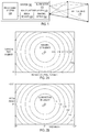
- FIG. 2A illustrates an example of sensing efficiency of an example image capture system.
- the sensing efficiency of a pixel sensor in an imaging system may be defined as or determined from a ratio of the intensity sensed by the pixel sensor to the intensity of light originating from the region or angular range in a field of view corresponding to the pixel.
- Such sensing efficiency may be exemplified for an ideal image capture system by considering a uniform field, e.g., a white screen that is uniformly lit and sensed, by the sensory array in the image capture system, as uniformly lit.
- a sensor array in the image capture system would ideally measure uniform intensity across the area of the sensor array.
- different pixel sensors in the image sensor may measure different intensities, e.g., because of limits in the ability of the image capture system to collect light from different areas in the field of view. As shown in FIG.
- a typical image capture system subject to vignetting may have a highest sensing efficiency at the center of the field of view of the image capture system, which may be because the system is able to capture a larger fraction of the light originating at the center of the field of view.
- FIG. 2A shows the center of the field of view with peak sensing efficiency (assigned a relative value 1.0).
- the contours in FIG. 2A show how the sensing sensitivity falls for pixel sensors positioned nearer to the edges of the image sensor, which would result in vignetting of images and higher signal-to-noise ratios in pixel data associated pixels near the edges of the field of view.
- the lower measured intensity levels may cause the signal-to-noise ratio worsen as the signal-to-noise ratio often depends on the measured intensity levels.
- lower intensity levels may correspond to a higher signal-to-noise ratio at the corners of the field of view in FIG. 2A .
- Applying post-processing techniques in an attempt to improve an image quality at the corners of the field of view may cause an even higher (worse) signal-to-noise ratio. This may be especially problematic in certain imaging systems such as security cameras, time of flight cameras, depth sensing cameras, 3D imagers, night vision cameras, and the like.
- Illuminator 110 may provide illumination having an intensity distribution that is shaped to compensate for vignetting or other variations in sensing sensitivity.
- the illumination may have a pattern shaped in angular space.
- FIG. 2B shows a contour plot illustrating an intensity distribution, according to an implementation of the disclosed subject matter, that compensates for the non-uniform sensing efficiency illustrated in FIG. 2A .
- the illumination intensity within the field of view shown in FIG. 2B may be inversely proportional to the corresponding sensing efficiency within the field of view shown in FIG. 2A .
- the illumination in FIG. 2B is plotted as a function of angle relative to a ray from the illuminator 110 to the center of the field of view of the illuminator 110.
- Corresponding pixel sensors in an image capture system may detect light from respective angles for light from a scene within the field of view of the image capture system.
- FIG. 2B does not show illumination that would illuminate areas outside the field of view of the imaging system. No illumination is needed for imaging outside the field of view the imaging system, so the illuminator intensity from the illuminator 110 is not critical and may be zero outside the ranges of field-of-view angles.
- the illumination provided by an illuminator 110 is represented in FIG. 2B and has a lowest illuminated intensity (assigned a relative intensity factor of 1.0) at a center of the field of view.
- the illumination increases in intensity toward the edges of the field of view.
- the illumination has a relative intensity of 2.5, which is 250% of the illumination at the center of the field of view.
- An imaging system using such illumination may achieve uniform effective sensing efficiency across the sensing array if the increase in illumination intensity compensates for the decrease in sensing efficiency for image capture.
- the product of the relative sensitivity factor from FIG. 2A and the corresponding relative intensity factor from FIG. 2B is uniform.
- the product of relative capture factor 1.0 and relative illumination factor 1.0 is 1, and at the corners the product of relative capture factor 0.4 and relative illumination factor 2.5 is also 1.
- the illumination illustrated in FIG. 2A may fully or substantially fully compensate for vignetting or for variations in SNR caused in an image or in image data by the variable sensing efficiency illustrated in FIG. 2A .
- the image capture system may only capture reflected light for which the illuminator 110 is the original source. This may be achieved, at least approximately, through use of an image capture system that is sensitive only to the light having the characteristics, e.g., the polarization, frequency, or wavelength of light from the illuminator 110.
- the illuminator 110 may produce illumination in a narrow spectral band
- the image capture system may include a spectral filter tuned to the illumination band and allowing mostly light from the illuminator 110 to pass.
- the frequency of flashes of illumination from an illuminator 110 may be much higher than the frame rate of a camera and/or provide a phase difference relative to image capture in the camera so that time-of-flight calculations can use image data and determine distances to objects that the illuminator 110 illuminates.
- Variation on synchronous image detection techniques may be used in time-of-flight imaging.
- the camera or image capture system may capture ambient light and light from the illuminator 110 that is reflected from objects in the field of view.
- the illuminator 110 may provide illumination that is altered based on or adapted according to the ambient illumination that may be expected or measured for the field of view. For example, for a uniformly lit scene, the illuminator 110 may be operated to provide illumination that, when added to the uniform ambient light, provides the total intensities as shown in FIG. 2B and thereby compensates for the relative sensing efficiency illustrated in FIG. 2A .
- the ambient light in a scene may not be uniform and may exacerbate vignetting, and an illuminator 110 used with such ambient light may need to provide illumination that is shaped to compensate for effects caused by both limitations of the image capture system and the ambient lighting.
- the illuminator 110 therefore may need to compensate for illumination vignetting and imaging vignetting, requiring the illuminator 110 to produce stronger compensation than illustrated by the example of FIG. 2A and FIG. 2B .
- the image capture system may capture two or more sets of image data for a given scene.
- the two or more sets of image data may be collected, for example, by capturing back-to-back image data.
- a first image data may be collected when an illuminator 110 illuminates the scene.
- a second image data may be captured without the illumination from the illuminator 110 and may capture image data for the scene with ambient light illuminating the scene.
- a processing component such as a microprocessor, a microcontroller, or any other applicable processing component may be configured to manipulate the two or more sets of image data to produce improved image data that may be used for security systems, 3D systems, depth sensing, object recognition, night vision, biometric identification and sensing, or the like.
- Illuminator 110 of FIG. 1 may be implemented using a variety of different architectures.
- FIG. 3A illustrates components of an illuminator 300 including a light source 310 and optics 320.
- Light source 310 may be any component configured to emit light such as an LED or an array of LEDs
- optics 320 may include one or more optical elements such as Fresnel lenses, gratings, or other structures that alter or control the angular distributions or shape of illumination exiting optics 320.
- optics 320 may be attached to light source 310.
- Optics 320 for illuminator 300 of FIG. 3A may produce a rotationally symmetric illumination pattern and may be easier to design and fabricate, e.g., with circular optical elements.
- a rotationally symmetric illumination may result in significant amounts of wasted light, i.e., light outside field of view, when an image capture system has a rectangular field of view.
- FIG. 3B shows an illuminator 350 that employs optics 370 including rectangular optical elements to more efficiently use radiation from a light source 360 to provide illumination to a rectangular field of view.
- An illuminator using an LED as a light source may need an optical system, e.g., optics 320 or 370, that reshapes the angular dependence of the intensity distribution of light emitted from the light source. Accordingly, the optical system may be designed according to the light emission characteristics of the light source.
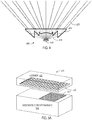
- FIG. 4 shows a cross-sectional view of an illuminator 400 including a light source 410 that may be an LED or other light emitting devices that emits light 415 that diverges from a source area.
- an illuminator 110 includes an array of LEDs and an array of optical elements to shape illumination and direct illumination from the LEDs into a rectangular field of view.
- U.S. Pat. No. 8,729,571 entitled “Multiple die LED and lens optical system,” for example, discloses architectures for LED arrays or systems having controlled distributions of light.
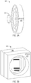
- FIG. 5A illustrates components of an illuminator 500 wherein an array of semiconductor lasers with a diffuser as the primary optic is employed.
- Illuminator 500 includes an integrated circuit package 510 containing an array 512 of vertical cavity surface emitting lasers (VCSELs) or other semiconductor lasers.
- a diffuser 520 is shown in FIG. 5A on a carrier 522 that may be used during fabrication of diffuser 520 or for attachment of diffuser 520 to integrated circuit package 510 in the assembled illuminator 500 as shown in FIG. 5B .
- Diffuser 520 may be an engineered diffuser with carefully controlled characteristics, e.g., an array of microlenses or other optical elements with predefined shapes and positions.
- the distribution of illumination from illuminator 500 may be further controlled by the electrical power or currents respectively applied to the lasers in array 512. More generally, some light emitters may be close to point sources but will have some size or extent for each light emitting area, and an optical system tends to create a distorted image of the light emitting area. Commonly, the light from the periphery of a light emitting area, e.g., edges of an LED chip, tends to illuminate the periphery of a spot or scene.
- the spatial distribution of light from an extended source such as array 512 thus may be set or altered to impact the angular radiation pattern the illumination out of an optic such as diffuser 520.
- FIG. 6 shows an illuminator 600 that uses a light source 610 that is extended and spatially non-uniform to produce a desired angular distribution for intensity in output illumination.
- Light source 610 may be made of multiple and perhaps individually addressable individual emitters, e.g., a VCSEL array, or may be one extended source producing a spatial distribution of illumination that varies over the light emitting area of the extended source. In the illustrated configuration, light source 610 is positioned to produce light originating from a focal plane of optical system 620.
- optical system 620 is a lens, but other or more complex optical systems may be employed to translate spatial positions on light source 610 to far field angles or to otherwise correlate spatial and angular distributions of light.
- optical system 620 directs or projects light from different areas of light source 610 to different the far field angles.
- optical system 620 directs light that originated from an area 612 of light source 610 on the optical axis of optical system 620 as light 622 parallel to the optical axis, but optical system 620 directs light 624 from an off-axis area 614 of light source 610 along a direction that depends on the focal length f of optical system 620 and on the position of area 614 relative to the optical axis of optical system 620.
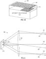
- Processing system 700 may specifically include a processor 730 with associated processing hardware that permits processor 730 to access data, e.g., image data 745, and execute instructions, e.g., software or firmware, that may be stored in a memory 740.
- processor 730 may, for example, include one or more central processing units (CPUs) or processing cores capable of executing program instructions and may include hardware that enables the CPUs or cores to control operation of connected devices such as illuminator 710 and image capture 720.
- CPUs central processing units
- processing cores capable of executing program instructions
- connected devices such as illuminator 710 and image capture 720.
- Memory 740 may include volatile or nonvolatile random access memory (RAM) that makes up a portion of the address space of processor 730.
- FIG. 7 illustrates an example implementation in which memory 740 for processor 730 contains a set of executable program modules 742, 744, 746, and 748.
- Such modules 742, 744, 746, and 748 may also be stored in or on a storage medium or device 770, which may for example include a hard drive or a removable memory device, instead of or in addition to being in addressable memory.
- Modules 742, 744, 746, and 748 may have a variety of purposes and may be selectively executed when system 700 perform specific processes or functions.
- processor 730 may execute a user interface 742 to control input and output devices in system 700 and to receive commands or information or to provide information or content.
- system 700 includes interface hardware 760, which may include input devices such as switches, buttons, a keypad, a keyboard, a mouse, a touch screen, or a microphone that a user may operate to provide input or commands, and processor 730 may execute user interface 742 to control the input devices and interpret user actions.
- Interface hardware 760 also may also include conventional output devices such as speakers, an audio system, or a touch screen or other display, and processor 730 may execute user interface 742 to output information via the output devices.
- Interface hardware 760 may further include network interfaces that enable system 700 to receive or transmit information through a network such as a local area network, a wide area network, a telecommunication network, or the Internet.
- Processor 730 may execute image capture control module 744 when using image capture system 720 to capture data, for example, in response to a command to capture an image with image capture system 720 or a command to change the settings, e.g., focus, aperture, filter, or lens, used in image capture system 720.
- illuminator 710 when image capture is initiated, produces illumination that is shaped to compensate for limitations of image capture system 720, for example, to reduce vignetting in captured image data.
- processor 730 may execute illuminator control module 746 to control when and how illuminator 710 operates. The particular illuminator control process will generally depend on the capabilities of illuminator 710.
- execution of illuminator control module 746 may identify a target illumination based on the current settings of image capture system 720, i.e., based on the focus, aperture, filter, or other features currently being used image capture system 720.
- the process resulting from execution of illuminator control module 746 may further detect ambient lighting in field of view 750 and may operate illuminator 710 to direct illumination into field of view 750 that alone or in combination with the ambient lighting achieves the identified target illumination for field of view 750.
- the captured image data may have a more uniform SNR than would be achieved with the ambient lighting or with conventional flash or lighting systems.
- Image data 745 in memory 740 may represent one or more images or frames captured by system 700.
- System 700 in addition to capturing image data 745 may process the image data.
- processor 730 may execute image processing module 748 to perform a processing function such as recognizing objects represented in image data 745, extracting depth or distance information for objects represented in image data 745, doing color corrections of image data 745, or performing spectral analysis if image data 745.
- Systems and methods such as described above may employ shaped illumination to compensate for unwanted effects such as vignetting and may provide image data having a more uniform SNR across an image. Such systems and methods may be particularly useful where the image data may need to be further processed for machine vision, object recognition, 3D modeling, or other purposes. Some applications that may particularly benefit from these capabilities include but are not limited to security cameras, 3D cameras, depth sensing, object recognition, night vision cameras, biometric identification cameras, and biometric sensing cameras.
Landscapes
- Engineering & Computer Science (AREA)
- Multimedia (AREA)
- Signal Processing (AREA)
- Physics & Mathematics (AREA)
- Spectroscopy & Molecular Physics (AREA)
- Studio Devices (AREA)
- Image Input (AREA)
Claims (15)
- Système comprenant :un système de capture d'image (120, 720) ayant une efficacité de détection qui varie sur un champ de vision du système de capture d'image ;un dispositif d'éclairage (110, 710) configuré pour éclairer le champ de vision du système de capture d'image, le dispositif d'éclairage étant configuré pour générer un éclairage ayant une distribution façonnée pour avoir une intensité plus élevée à l'endroit où l'efficacité de détection est plus faible ;caractérisé parun composant de traitement (130, 730) configuré pour combiner des premières données d'image correspondant à une scène éclairée par le dispositif d'éclairage avec des deuxièmes données d'image correspondant à la scène avec un éclairage ambiant pour produire des troisièmes données d'image qui ont un rapport signal sur bruit sensiblement uniforme.
- Système selon la revendication 1, dans lequel les troisièmes données d'image sont configurées pour représenter une scène capturée par le système de capture d'image.
- Système selon la revendication 1, dans lequel l'éclairage a une intensité au niveau d'un centre du champ de vision qui est inférieure à une intensité de l'éclairage au niveau d'un bord du champ de vision.
- Système selon la revendication 1, dans lequel le dispositif d'éclairage comprend :une source de lumière ; etune optique de façonnage qui dirige une première intensité de lumière provenant de la source de lumière vers une première zone du champ de vision et qui dirige une seconde intensité de la lumière provenant de la source de lumière vers une seconde zone du champ de vision, dans lequel la seconde zone correspond à l'endroit où l'efficacité de détection du système de capture d'image est plus faible ; etla seconde intensité étant supérieure à la première intensité.
- Système selon la revendication 4, dans lequel la source de lumière produit de la lumière provenant d'une zone de source et la lumière provenant de la zone de source est non uniforme dans l'espace.
- Système selon la revendication 5, dans lequel la source de lumière comprend une pluralité d'éléments de lumière qui sont distribués sur la zone de source et utilisés pour produire l'éclairage non uniforme dans l'espace.
- Système selon la revendication 4, dans lequel l'optique de façonnage modifie l'éclairage provenant de la source de lumière de sorte que l'éclairage provenant du dispositif d'éclairage a une section transversale rectangulaire.
- Système selon la revendication 4, dans lequel l'optique de façonnage comprend une lentille, et la zone de source est située dans un plan focal de la lentille.
- Système selon la revendication 1, dans lequel le dispositif d'éclairage produit un éclairage symétrique en rotation.
- Système selon la revendication 1, dans lequel le dispositif d'éclairage comprend un réseau de lasers à semi-conducteur.
- Système selon la revendication 10, dans lequel le dispositif d'éclairage comprend en outre un diffuseur positionné pour contrôler une divergence de faisceaux provenant des lasers à semi-conducteur.
- Système selon la revendication 1, dans lequel le système est choisi dans un groupe constitué d'une caméra, d'un téléphone mobile, d'un ordinateur, d'un système de reconnaissance d'objets et d'un système de mesure de temps de vol.
- Procédé de collecte de données d'image comprenant :la détermination de l'efficacité de détection d'un système de capture d'image (120, 720) au niveau d'une pluralité de points ;l'éclairage d'une scène, l'éclairage (110, 710) ayant une distribution façonnée avec une intensité plus élevée à l'endroit où l'efficacité de détection du système de capture d'image est plus faible ;l'utilisation du système de capture d'image pour capturer des premières données d'image représentant la scène telle qu'éclairée avec l'éclairage ayant la distribution façonnée ;l'utilisation du système de capture d'image pour capturer des deuxièmes données d'image représentant la scène à la lumière ambiante sans l'éclairage ayant la distribution façonnée ;caractérisé parla combinaison des premières données d'image et des deuxièmes données d'image pour produire des troisièmes données d'image qui ont un rapport signal sur bruit sensiblement uniforme.
- Procédé selon la revendication 13, dans lequel l'éclairage est plus lumineux au niveau d'une périphérie d'un champ de vision du système d'imagerie que l'éclairage au niveau d'un centre du champ de vision du système d'imagerie.
- Procédé selon la revendication 13, dans lequel le système de capture d'image est configuré pour capturer les premières données d'image représentant la scène telle qu'éclairée avec l'éclairage ayant la distribution façonnée sur la base d'une caractéristique de l'éclairage, dans lequel les caractéristiques de l'éclairage incluent au moins une d'une polarisation, d'une longueur d'onde ou d'une fréquence.
Applications Claiming Priority (4)
| Application Number | Priority Date | Filing Date | Title |
|---|---|---|---|
| US201662438956P | 2016-12-23 | 2016-12-23 | |
| EP17168779 | 2017-04-28 | ||
| US15/851,240 US10582169B2 (en) | 2016-12-23 | 2017-12-21 | Compensating for vignetting |
| PCT/US2017/068087 WO2018119345A1 (fr) | 2016-12-23 | 2017-12-22 | Compensation de vignettage |
Publications (2)
| Publication Number | Publication Date |
|---|---|
| EP3560184A1 EP3560184A1 (fr) | 2019-10-30 |
| EP3560184B1 true EP3560184B1 (fr) | 2021-04-21 |
Family
ID=60955412
Family Applications (1)
| Application Number | Title | Priority Date | Filing Date |
|---|---|---|---|
| EP17828824.7A Active EP3560184B1 (fr) | 2016-12-23 | 2017-12-22 | Compensation de vignettage |
Country Status (4)
| Country | Link |
|---|---|
| EP (1) | EP3560184B1 (fr) |
| JP (1) | JP7386703B2 (fr) |
| KR (1) | KR102258568B1 (fr) |
| CN (2) | CN110383803A (fr) |
Families Citing this family (2)
| Publication number | Priority date | Publication date | Assignee | Title |
|---|---|---|---|---|
| US10582169B2 (en) | 2016-12-23 | 2020-03-03 | Lumileds Llc | Compensating for vignetting |
| WO2022241778A1 (fr) * | 2021-05-21 | 2022-11-24 | 深圳市汇顶科技股份有限公司 | Appareil de transmission pour détection de profondeur de temps de vol et dispositif électronique |
Family Cites Families (13)
| Publication number | Priority date | Publication date | Assignee | Title |
|---|---|---|---|---|
| GB2372391A (en) * | 2001-02-16 | 2002-08-21 | Hewlett Packard Co | Removal of specular reflection |
| US20050046739A1 (en) * | 2003-08-29 | 2005-03-03 | Voss James S. | System and method using light emitting diodes with an image capture device |
| US20070153495A1 (en) | 2005-12-29 | 2007-07-05 | Wang Michael Dongxue | Illumination mechanism for mobile digital imaging |
| JP4747065B2 (ja) * | 2006-09-29 | 2011-08-10 | 富士通株式会社 | 画像生成装置、画像生成方法および画像生成プログラム |
| US7697062B2 (en) * | 2006-11-08 | 2010-04-13 | Sony Ericsson Mobile Communications Ab | Camera and method in a camera |
| US8371713B2 (en) * | 2007-09-13 | 2013-02-12 | Koninklijke Philips Electronics N.V. | Illumination device for pixelated illumination |
| US8922672B2 (en) * | 2008-01-03 | 2014-12-30 | Apple Inc. | Illumination systems and methods for imagers |
| JP2009176471A (ja) | 2008-01-22 | 2009-08-06 | Stanley Electric Co Ltd | Led光源用レンズ |
| US8223260B2 (en) * | 2008-07-25 | 2012-07-17 | Research In Motion Limited | Electronic device having a camera and method of controlling a flash |
| JP5756722B2 (ja) * | 2011-06-22 | 2015-07-29 | 株式会社エンプラス | 光束制御部材、発光装置および照明装置 |
| WO2014087301A1 (fr) * | 2012-12-05 | 2014-06-12 | Koninklijke Philips N.V. | Matrice d'éclairage avec distribution adaptée du rayonnement |
| DE102013202890B4 (de) | 2013-02-22 | 2018-12-06 | Schaeffler Technologies AG & Co. KG | Verfahren zur Erzeugung eines Audiosignal für ein synthetisches Geräusch eines Kraftfahrzeuges |
| US9635231B2 (en) * | 2014-12-22 | 2017-04-25 | Google Inc. | Time-of-flight camera system and method to improve measurement quality of weak field-of-view signal regions |
-
2017
- 2017-12-22 KR KR1020197021424A patent/KR102258568B1/ko active IP Right Grant
- 2017-12-22 CN CN201780087293.3A patent/CN110383803A/zh active Pending
- 2017-12-22 EP EP17828824.7A patent/EP3560184B1/fr active Active
- 2017-12-22 JP JP2019534379A patent/JP7386703B2/ja active Active
- 2017-12-22 CN CN202110678977.9A patent/CN113329140A/zh active Pending
Also Published As
| Publication number | Publication date |
|---|---|
| JP2020515100A (ja) | 2020-05-21 |
| CN113329140A (zh) | 2021-08-31 |
| KR20190099044A (ko) | 2019-08-23 |
| EP3560184A1 (fr) | 2019-10-30 |
| JP7386703B2 (ja) | 2023-11-27 |
| CN110383803A (zh) | 2019-10-25 |
| KR102258568B1 (ko) | 2021-05-28 |
Similar Documents
| Publication | Publication Date | Title |
|---|---|---|
| US10893244B2 (en) | Compensating for vignetting | |
| US11575843B2 (en) | Image sensor modules including primary high-resolution imagers and secondary imagers | |
| TWI565323B (zh) | 分辨前景的成像裝置及其運作方法、以及影像感測器 | |
| US20150326771A1 (en) | Imaging device and exposure adjusting method | |
| TW201544848A (zh) | 包括用於不同波長之獨立成像器之結構化立體成像組件 | |
| TWI801637B (zh) | 用於相機之紅外光預閃光 | |
| EP3560184B1 (fr) | Compensation de vignettage | |
| JP7401013B2 (ja) | 情報処理装置、制御装置、情報処理方法及びプログラム | |
| TW201543130A (zh) | 攝像控制裝置 | |
| US11423528B2 (en) | Image inspection apparatus | |
| US10853935B2 (en) | Image processing system, computer readable recording medium, and image processing method | |
| US9906705B2 (en) | Image pickup apparatus | |
| US10859506B2 (en) | Image processing system for processing image data generated in different light emission states, non-transitory computer readable recording medium, and image processing method | |
| KR102027106B1 (ko) | 콘트라스트가 향상된 영상취득장치 및 방법, 이를 위한 컴퓨터 프로그램 및 기록매체 | |
| WO2015146084A1 (fr) | Terminal de point de vente, dispositif de traitement d'informations, procédé d'ajustement de balance des blancs, et support d'enregistrement | |
| US11831859B2 (en) | Passive three-dimensional image sensing based on referential image blurring with spotted reference illumination | |
| JP6386837B2 (ja) | 画像処理プログラム、情報処理システム、情報処理装置、画像処理方法 | |
| US11582436B2 (en) | Passive three-dimensional image sensing based on chromatic focal differentiation | |
| JP7080724B2 (ja) | 配光制御装置、投光システム及び配光制御方法 | |
| US20210118171A1 (en) | Object characteristic locating device and laser and imaging integration system | |
| JP2020095454A (ja) | 処理装置、撮像装置、処理システム、処理方法、プログラム、および、記憶媒体 | |
| CN110598685A (zh) | 分辨前景的成像装置 |
Legal Events
| Date | Code | Title | Description |
|---|---|---|---|
| STAA | Information on the status of an ep patent application or granted ep patent |
Free format text: STATUS: UNKNOWN |
|
| STAA | Information on the status of an ep patent application or granted ep patent |
Free format text: STATUS: THE INTERNATIONAL PUBLICATION HAS BEEN MADE |
|
| PUAI | Public reference made under article 153(3) epc to a published international application that has entered the european phase |
Free format text: ORIGINAL CODE: 0009012 |
|
| STAA | Information on the status of an ep patent application or granted ep patent |
Free format text: STATUS: REQUEST FOR EXAMINATION WAS MADE |
|
| 17P | Request for examination filed |
Effective date: 20190723 |
|
| AK | Designated contracting states |
Kind code of ref document: A1 Designated state(s): AL AT BE BG CH CY CZ DE DK EE ES FI FR GB GR HR HU IE IS IT LI LT LU LV MC MK MT NL NO PL PT RO RS SE SI SK SM TR |
|
| AX | Request for extension of the european patent |
Extension state: BA ME |
|
| RIN1 | Information on inventor provided before grant (corrected) |
Inventor name: ENGELEN, ROB JACQUES PAUL |
|
| DAV | Request for validation of the european patent (deleted) | ||
| DAX | Request for extension of the european patent (deleted) | ||
| GRAP | Despatch of communication of intention to grant a patent |
Free format text: ORIGINAL CODE: EPIDOSNIGR1 |
|
| STAA | Information on the status of an ep patent application or granted ep patent |
Free format text: STATUS: GRANT OF PATENT IS INTENDED |
|
| INTG | Intention to grant announced |
Effective date: 20210120 |
|
| GRAS | Grant fee paid |
Free format text: ORIGINAL CODE: EPIDOSNIGR3 |
|
| GRAA | (expected) grant |
Free format text: ORIGINAL CODE: 0009210 |
|
| STAA | Information on the status of an ep patent application or granted ep patent |
Free format text: STATUS: THE PATENT HAS BEEN GRANTED |
|
| AK | Designated contracting states |
Kind code of ref document: B1 Designated state(s): AL AT BE BG CH CY CZ DE DK EE ES FI FR GB GR HR HU IE IS IT LI LT LU LV MC MK MT NL NO PL PT RO RS SE SI SK SM TR |
|
| REG | Reference to a national code |
Ref country code: GB Ref legal event code: FG4D |
|
| REG | Reference to a national code |
Ref country code: CH Ref legal event code: EP |
|
| REG | Reference to a national code |
Ref country code: DE Ref legal event code: R096 Ref document number: 602017037288 Country of ref document: DE Ref country code: IE Ref legal event code: FG4D |
|
| REG | Reference to a national code |
Ref country code: AT Ref legal event code: REF Ref document number: 1385840 Country of ref document: AT Kind code of ref document: T Effective date: 20210515 |
|
| REG | Reference to a national code |
Ref country code: LT Ref legal event code: MG9D |
|
| REG | Reference to a national code |
Ref country code: AT Ref legal event code: MK05 Ref document number: 1385840 Country of ref document: AT Kind code of ref document: T Effective date: 20210421 |
|
| REG | Reference to a national code |
Ref country code: NL Ref legal event code: MP Effective date: 20210421 |
|
| PG25 | Lapsed in a contracting state [announced via postgrant information from national office to epo] |
Ref country code: FI Free format text: LAPSE BECAUSE OF FAILURE TO SUBMIT A TRANSLATION OF THE DESCRIPTION OR TO PAY THE FEE WITHIN THE PRESCRIBED TIME-LIMIT Effective date: 20210421 Ref country code: LT Free format text: LAPSE BECAUSE OF FAILURE TO SUBMIT A TRANSLATION OF THE DESCRIPTION OR TO PAY THE FEE WITHIN THE PRESCRIBED TIME-LIMIT Effective date: 20210421 Ref country code: NL Free format text: LAPSE BECAUSE OF FAILURE TO SUBMIT A TRANSLATION OF THE DESCRIPTION OR TO PAY THE FEE WITHIN THE PRESCRIBED TIME-LIMIT Effective date: 20210421 Ref country code: AT Free format text: LAPSE BECAUSE OF FAILURE TO SUBMIT A TRANSLATION OF THE DESCRIPTION OR TO PAY THE FEE WITHIN THE PRESCRIBED TIME-LIMIT Effective date: 20210421 Ref country code: BG Free format text: LAPSE BECAUSE OF FAILURE TO SUBMIT A TRANSLATION OF THE DESCRIPTION OR TO PAY THE FEE WITHIN THE PRESCRIBED TIME-LIMIT Effective date: 20210721 Ref country code: HR Free format text: LAPSE BECAUSE OF FAILURE TO SUBMIT A TRANSLATION OF THE DESCRIPTION OR TO PAY THE FEE WITHIN THE PRESCRIBED TIME-LIMIT Effective date: 20210421 |
|
| PG25 | Lapsed in a contracting state [announced via postgrant information from national office to epo] |
Ref country code: NO Free format text: LAPSE BECAUSE OF FAILURE TO SUBMIT A TRANSLATION OF THE DESCRIPTION OR TO PAY THE FEE WITHIN THE PRESCRIBED TIME-LIMIT Effective date: 20210721 Ref country code: LV Free format text: LAPSE BECAUSE OF FAILURE TO SUBMIT A TRANSLATION OF THE DESCRIPTION OR TO PAY THE FEE WITHIN THE PRESCRIBED TIME-LIMIT Effective date: 20210421 Ref country code: PT Free format text: LAPSE BECAUSE OF FAILURE TO SUBMIT A TRANSLATION OF THE DESCRIPTION OR TO PAY THE FEE WITHIN THE PRESCRIBED TIME-LIMIT Effective date: 20210823 Ref country code: PL Free format text: LAPSE BECAUSE OF FAILURE TO SUBMIT A TRANSLATION OF THE DESCRIPTION OR TO PAY THE FEE WITHIN THE PRESCRIBED TIME-LIMIT Effective date: 20210421 Ref country code: SE Free format text: LAPSE BECAUSE OF FAILURE TO SUBMIT A TRANSLATION OF THE DESCRIPTION OR TO PAY THE FEE WITHIN THE PRESCRIBED TIME-LIMIT Effective date: 20210421 Ref country code: RS Free format text: LAPSE BECAUSE OF FAILURE TO SUBMIT A TRANSLATION OF THE DESCRIPTION OR TO PAY THE FEE WITHIN THE PRESCRIBED TIME-LIMIT Effective date: 20210421 Ref country code: IS Free format text: LAPSE BECAUSE OF FAILURE TO SUBMIT A TRANSLATION OF THE DESCRIPTION OR TO PAY THE FEE WITHIN THE PRESCRIBED TIME-LIMIT Effective date: 20210821 Ref country code: GR Free format text: LAPSE BECAUSE OF FAILURE TO SUBMIT A TRANSLATION OF THE DESCRIPTION OR TO PAY THE FEE WITHIN THE PRESCRIBED TIME-LIMIT Effective date: 20210722 |
|
| REG | Reference to a national code |
Ref country code: DE Ref legal event code: R097 Ref document number: 602017037288 Country of ref document: DE |
|
| PG25 | Lapsed in a contracting state [announced via postgrant information from national office to epo] |
Ref country code: SM Free format text: LAPSE BECAUSE OF FAILURE TO SUBMIT A TRANSLATION OF THE DESCRIPTION OR TO PAY THE FEE WITHIN THE PRESCRIBED TIME-LIMIT Effective date: 20210421 Ref country code: SK Free format text: LAPSE BECAUSE OF FAILURE TO SUBMIT A TRANSLATION OF THE DESCRIPTION OR TO PAY THE FEE WITHIN THE PRESCRIBED TIME-LIMIT Effective date: 20210421 Ref country code: ES Free format text: LAPSE BECAUSE OF FAILURE TO SUBMIT A TRANSLATION OF THE DESCRIPTION OR TO PAY THE FEE WITHIN THE PRESCRIBED TIME-LIMIT Effective date: 20210421 Ref country code: EE Free format text: LAPSE BECAUSE OF FAILURE TO SUBMIT A TRANSLATION OF THE DESCRIPTION OR TO PAY THE FEE WITHIN THE PRESCRIBED TIME-LIMIT Effective date: 20210421 Ref country code: DK Free format text: LAPSE BECAUSE OF FAILURE TO SUBMIT A TRANSLATION OF THE DESCRIPTION OR TO PAY THE FEE WITHIN THE PRESCRIBED TIME-LIMIT Effective date: 20210421 Ref country code: CZ Free format text: LAPSE BECAUSE OF FAILURE TO SUBMIT A TRANSLATION OF THE DESCRIPTION OR TO PAY THE FEE WITHIN THE PRESCRIBED TIME-LIMIT Effective date: 20210421 Ref country code: RO Free format text: LAPSE BECAUSE OF FAILURE TO SUBMIT A TRANSLATION OF THE DESCRIPTION OR TO PAY THE FEE WITHIN THE PRESCRIBED TIME-LIMIT Effective date: 20210421 |
|
| PLBE | No opposition filed within time limit |
Free format text: ORIGINAL CODE: 0009261 |
|
| STAA | Information on the status of an ep patent application or granted ep patent |
Free format text: STATUS: NO OPPOSITION FILED WITHIN TIME LIMIT |
|
| 26N | No opposition filed |
Effective date: 20220124 |
|
| PG25 | Lapsed in a contracting state [announced via postgrant information from national office to epo] |
Ref country code: IS Free format text: LAPSE BECAUSE OF FAILURE TO SUBMIT A TRANSLATION OF THE DESCRIPTION OR TO PAY THE FEE WITHIN THE PRESCRIBED TIME-LIMIT Effective date: 20210821 Ref country code: AL Free format text: LAPSE BECAUSE OF FAILURE TO SUBMIT A TRANSLATION OF THE DESCRIPTION OR TO PAY THE FEE WITHIN THE PRESCRIBED TIME-LIMIT Effective date: 20210421 |
|
| PG25 | Lapsed in a contracting state [announced via postgrant information from national office to epo] |
Ref country code: MC Free format text: LAPSE BECAUSE OF FAILURE TO SUBMIT A TRANSLATION OF THE DESCRIPTION OR TO PAY THE FEE WITHIN THE PRESCRIBED TIME-LIMIT Effective date: 20210421 Ref country code: IT Free format text: LAPSE BECAUSE OF FAILURE TO SUBMIT A TRANSLATION OF THE DESCRIPTION OR TO PAY THE FEE WITHIN THE PRESCRIBED TIME-LIMIT Effective date: 20210421 |
|
| REG | Reference to a national code |
Ref country code: CH Ref legal event code: PL |
|
| REG | Reference to a national code |
Ref country code: BE Ref legal event code: MM Effective date: 20211231 |
|
| PG25 | Lapsed in a contracting state [announced via postgrant information from national office to epo] |
Ref country code: LU Free format text: LAPSE BECAUSE OF NON-PAYMENT OF DUE FEES Effective date: 20211222 Ref country code: IE Free format text: LAPSE BECAUSE OF NON-PAYMENT OF DUE FEES Effective date: 20211222 |
|
| REG | Reference to a national code |
Ref country code: DE Ref legal event code: R079 Ref document number: 602017037288 Country of ref document: DE Free format text: PREVIOUS MAIN CLASS: H04N0005217000 Ipc: H04N0023800000 |
|
| PG25 | Lapsed in a contracting state [announced via postgrant information from national office to epo] |
Ref country code: BE Free format text: LAPSE BECAUSE OF NON-PAYMENT OF DUE FEES Effective date: 20211231 |
|
| PG25 | Lapsed in a contracting state [announced via postgrant information from national office to epo] |
Ref country code: LI Free format text: LAPSE BECAUSE OF NON-PAYMENT OF DUE FEES Effective date: 20211231 Ref country code: CH Free format text: LAPSE BECAUSE OF NON-PAYMENT OF DUE FEES Effective date: 20211231 |
|
| PG25 | Lapsed in a contracting state [announced via postgrant information from national office to epo] |
Ref country code: CY Free format text: LAPSE BECAUSE OF FAILURE TO SUBMIT A TRANSLATION OF THE DESCRIPTION OR TO PAY THE FEE WITHIN THE PRESCRIBED TIME-LIMIT Effective date: 20210421 |
|
| P01 | Opt-out of the competence of the unified patent court (upc) registered |
Effective date: 20230530 |
|
| PG25 | Lapsed in a contracting state [announced via postgrant information from national office to epo] |
Ref country code: HU Free format text: LAPSE BECAUSE OF FAILURE TO SUBMIT A TRANSLATION OF THE DESCRIPTION OR TO PAY THE FEE WITHIN THE PRESCRIBED TIME-LIMIT; INVALID AB INITIO Effective date: 20171222 |
|
| PGFP | Annual fee paid to national office [announced via postgrant information from national office to epo] |
Ref country code: GB Payment date: 20231219 Year of fee payment: 7 |
|
| PGFP | Annual fee paid to national office [announced via postgrant information from national office to epo] |
Ref country code: FR Payment date: 20231226 Year of fee payment: 7 |
|
| PG25 | Lapsed in a contracting state [announced via postgrant information from national office to epo] |
Ref country code: MK Free format text: LAPSE BECAUSE OF FAILURE TO SUBMIT A TRANSLATION OF THE DESCRIPTION OR TO PAY THE FEE WITHIN THE PRESCRIBED TIME-LIMIT Effective date: 20210421 |
|
| PGFP | Annual fee paid to national office [announced via postgrant information from national office to epo] |
Ref country code: DE Payment date: 20231227 Year of fee payment: 7 |