EP3559994B1 - Multispektraler sensor mit gestapelten photodetektoren - Google Patents
Multispektraler sensor mit gestapelten photodetektoren Download PDFInfo
- Publication number
- EP3559994B1 EP3559994B1 EP17821580.2A EP17821580A EP3559994B1 EP 3559994 B1 EP3559994 B1 EP 3559994B1 EP 17821580 A EP17821580 A EP 17821580A EP 3559994 B1 EP3559994 B1 EP 3559994B1
- Authority
- EP
- European Patent Office
- Prior art keywords
- cathode
- photodetector
- anode
- face
- interest
- Prior art date
- Legal status (The legal status is an assumption and is not a legal conclusion. Google has not performed a legal analysis and makes no representation as to the accuracy of the status listed.)
- Active
Links
Images




Classifications
-
- H—ELECTRICITY
- H10—SEMICONDUCTOR DEVICES; ELECTRIC SOLID-STATE DEVICES NOT OTHERWISE PROVIDED FOR
- H10F—INORGANIC SEMICONDUCTOR DEVICES SENSITIVE TO INFRARED RADIATION, LIGHT, ELECTROMAGNETIC RADIATION OF SHORTER WAVELENGTH OR CORPUSCULAR RADIATION
- H10F30/00—Individual radiation-sensitive semiconductor devices in which radiation controls the flow of current through the devices, e.g. photodetectors
- H10F30/20—Individual radiation-sensitive semiconductor devices in which radiation controls the flow of current through the devices, e.g. photodetectors the devices having potential barriers, e.g. phototransistors
- H10F30/21—Individual radiation-sensitive semiconductor devices in which radiation controls the flow of current through the devices, e.g. photodetectors the devices having potential barriers, e.g. phototransistors the devices being sensitive to infrared, visible or ultraviolet radiation
- H10F30/288—Individual radiation-sensitive semiconductor devices in which radiation controls the flow of current through the devices, e.g. photodetectors the devices having potential barriers, e.g. phototransistors the devices being sensitive to infrared, visible or ultraviolet radiation the devices being sensitive to multiple wavelengths, e.g. multi-spectrum radiation detection devices
-
- H—ELECTRICITY
- H10—SEMICONDUCTOR DEVICES; ELECTRIC SOLID-STATE DEVICES NOT OTHERWISE PROVIDED FOR
- H10F—INORGANIC SEMICONDUCTOR DEVICES SENSITIVE TO INFRARED RADIATION, LIGHT, ELECTROMAGNETIC RADIATION OF SHORTER WAVELENGTH OR CORPUSCULAR RADIATION
- H10F39/00—Integrated devices, or assemblies of multiple devices, comprising at least one element covered by group H10F30/00, e.g. radiation detectors comprising photodiode arrays
- H10F39/10—Integrated devices
- H10F39/107—Integrated devices having multiple elements covered by H10F30/00 in a repetitive configuration, e.g. radiation detectors comprising photodiode arrays
-
- H—ELECTRICITY
- H10—SEMICONDUCTOR DEVICES; ELECTRIC SOLID-STATE DEVICES NOT OTHERWISE PROVIDED FOR
- H10F—INORGANIC SEMICONDUCTOR DEVICES SENSITIVE TO INFRARED RADIATION, LIGHT, ELECTROMAGNETIC RADIATION OF SHORTER WAVELENGTH OR CORPUSCULAR RADIATION
- H10F39/00—Integrated devices, or assemblies of multiple devices, comprising at least one element covered by group H10F30/00, e.g. radiation detectors comprising photodiode arrays
- H10F39/10—Integrated devices
- H10F39/12—Image sensors
- H10F39/18—Complementary metal-oxide-semiconductor [CMOS] image sensors; Photodiode array image sensors
- H10F39/182—Colour image sensors
- H10F39/1825—Multicolour image sensors having stacked structure, e.g. NPN, NPNPN or multiple quantum well [MQW] structures
-
- H—ELECTRICITY
- H10—SEMICONDUCTOR DEVICES; ELECTRIC SOLID-STATE DEVICES NOT OTHERWISE PROVIDED FOR
- H10F—INORGANIC SEMICONDUCTOR DEVICES SENSITIVE TO INFRARED RADIATION, LIGHT, ELECTROMAGNETIC RADIATION OF SHORTER WAVELENGTH OR CORPUSCULAR RADIATION
- H10F39/00—Integrated devices, or assemblies of multiple devices, comprising at least one element covered by group H10F30/00, e.g. radiation detectors comprising photodiode arrays
- H10F39/10—Integrated devices
- H10F39/12—Image sensors
- H10F39/18—Complementary metal-oxide-semiconductor [CMOS] image sensors; Photodiode array image sensors
- H10F39/184—Infrared image sensors
- H10F39/1847—Multispectral infrared image sensors having a stacked structure, e.g. NPN, NPNPN or multiple quantum well [MQW] structures
-
- H—ELECTRICITY
- H10—SEMICONDUCTOR DEVICES; ELECTRIC SOLID-STATE DEVICES NOT OTHERWISE PROVIDED FOR
- H10F—INORGANIC SEMICONDUCTOR DEVICES SENSITIVE TO INFRARED RADIATION, LIGHT, ELECTROMAGNETIC RADIATION OF SHORTER WAVELENGTH OR CORPUSCULAR RADIATION
- H10F77/00—Constructional details of devices covered by this subclass
- H10F77/10—Semiconductor bodies
- H10F77/14—Shape of semiconductor bodies; Shapes, relative sizes or dispositions of semiconductor regions within semiconductor bodies
- H10F77/148—Shapes of potential barriers
-
- H—ELECTRICITY
- H10—SEMICONDUCTOR DEVICES; ELECTRIC SOLID-STATE DEVICES NOT OTHERWISE PROVIDED FOR
- H10F—INORGANIC SEMICONDUCTOR DEVICES SENSITIVE TO INFRARED RADIATION, LIGHT, ELECTROMAGNETIC RADIATION OF SHORTER WAVELENGTH OR CORPUSCULAR RADIATION
- H10F77/00—Constructional details of devices covered by this subclass
- H10F77/20—Electrodes
Definitions
- the invention relates to a multispectral sensor.
- the resolution obtained is also limited because several photodetectors of the multispectral sensor are used to detect a color.
- the doping difference between two successive semiconductor regions of different type must be of the order of two decades to obtain defined and reproducible junction depths as well as a ZCE (Charge Zone of Space) significant.
- the formation of successive regions of different types is carried out by introducing for each region an additional concentration of impurities in order to achieve the desired doping.
- concentration of introduced impurities keeps increasing and can quickly reach the limit of impurity that can be introduced into the semiconductor.
- the temporal response of such a multispectral sensor is limited by the diffusion currents, which are generally greater than the transit currents, and by the non-negligible values of the junction capacitors.
- An objective of the invention is to resolve at least one of the aforementioned drawbacks.
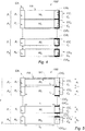
- FIG. 1 A first embodiment of a multispectral sensor in accordance with the invention is shown in figure 1 .
- the multispectral sensor 100 comprises a plurality of N photodetectors P 1 , ..., P N with N an integer such that N ⁇ 2.
- Each photodetector comprises an anode A 1 , ..., A N and a cathode C 1 , ..., C N separated from each other by a region of interest R I1 , ..., R IN .
- the anode, the cathode and the region of interest are made of a semiconductor material.
- the multi-spectral photodetector 100 also comprises at least one electrical contact AC for all of the N anodes A 1 , ..., A N as well as an electrical contact CC 1 , ..., CC N associated with each of the N cathodes.
- each electrical contact CA, CC 1 , ..., CC N can be made of a material chosen from a metal, a metal alloy or based on a degenerate doped poly-crystal such as poly-crystalline silicon.
- the photo-currents (or the photo-generated charged) in each photodetector P 1 , ..., P N are collected through the corresponding electrical contact CC 1 , ..., CC N. The photo-currents are thus collected separately without any charge redistribution between the cathodes.
- Each photodetector has a PIN type structure.
- the photodetectors P 1 , ..., P N are moreover stacked on top of each other so that the anodes A 1 , ..., A N on the one hand, the cathodes C 1 , ..., C N on the other hand and the regions of interest R I1 , ..., R IN finally of two consecutive photodetectors in the stack are arranged face to face.
- an insulation layer CIC 1 , CIC 2 , ..., CIC i-1 , CIC i , ..., CIC N-1 is provided between two cathodes who face each other. This makes it possible to prevent photo-currents generated in a given photodetector P i from being collected by a cathode associated with another photodetector.
- Each of these insulation layers can be produced with ion implantation, for example with P + type doping, on the corresponding cathode.
- the active face FA of the multi-spectral sensor 100 there is a face called the active face FA of the multi-spectral sensor 100, common to all the photodetectors of the stack, and defined by the face of the first region of interest RI 1 of the first photodetector P 1 of the stack through which photons are intended to enter the stack.
- This distance d i defines the depth at which the i th photodetector of the stack is located, within the multispectral sensor 100.
- this thickness is also possible to define the thickness e i of a photodetector P i , this thickness being in particular that of a region of interest of this photodetector P i .
- this thickness e i of a region of interest RI 1 , ..., RI N may be between a few tens of nm to several micrometers, for example between 20 nm and 5 microns.
- each region of interest of the stack absorbs wavelengths according to a “bell” curve centered on the wavelength of interest (wavelength of the peak of the bell).
- the depth d i at which a photodetector P i with 1 ⁇ i ⁇ N is located within the stack and the thickness e i of this photodetector P i , and more precisely of a region of interest RI i with 1 ⁇ i N, make it possible to define the wavelength of interest and the width at mid height (around the peak) of the “bell” curve, this width at mid-height defining the wavelength selectivity of the photodetector considered.
- each photodetector P 1 , ..., P N of the stack is dedicated to the detection of a given range of wavelengths of interest and that the multispectral character of the multispectral sensor comes from the presence of a plurality of stacked photodetectors as proposed in the context of the invention. It will also be understood that the presence of an electrical contact CC i for each photodetector P i is important for applying the necessary reverse bias and for being able to measure the photo-generated electrical signal in each photodetector.
- the arrangement of the multi-spectral sensor 100 will make it possible to detect the shortest wavelengths close to the active face FA and increasingly larger wavelengths as the distance d i of the photodetector is deep in the stack.
- each photodetector P 1 , ..., P N will be chosen as a function of the wavelength range that is to be analyzed.
- silicon (Si) for a wavelength range comprised between 0.2 ⁇ m and 1.1 ⁇ m
- germanium (Ge) for a wavelength comprised between 0.2 ⁇ m and 1.7 ⁇ m.
- GaAs Gallium Arsenide
- Gallium-Indium Arsenide for the wavelength range from 1 ⁇ m to 1.7 ⁇ m
- Indium Arsenide Aln
- Indium Antimonide InSb
- Mercury-Cadnium Telluride HgCdTe
- the number N of photodetectors P 1 , ..., P N will be determined as a function of the range of wavelengths that one wishes to analyze with the multispectral sensor 100 and the selectivity of the desired decomposition.
- the number N of photodetectors in the stack is limited only by the total depth or thickness of the stack, which must not exceed a value corresponding to a total absorption of the incident photons. Indeed, from a certain depth or total thickness, the photons are completely absorbed and no longer penetrate into the material. In this case, a thicker stack is of no interest.
- the width I i can be defined with 1 i N of a region of interest R I1 , ..., R IN of each photodetector P 1 , ..., P N of the stack. This width I i is taken perpendicular to the depth of the stack.
- this width I i of a photodetector P i depends on the envisaged application. Certain applications require small size photodetectors (also called pixels), that is to say having an area of 1 ⁇ m 2 to 6 ⁇ m 2 ) in order to increase the spatial resolution and the definition of the captured image. Other applications require large-size sensors, for example in order to increase sensitivity in low-light conditions (large-area image sensors for telescopes, for example). Thus, for an image sensor, this width I i of a region of interest RI 1 , ..., RI N may be between a few hundred nanometers and a few microns or even tens of microns, for example between 200nm and 50 microns.
- It can be of the order of a few hundred microns for specific sensors, namely between 200 microns to 800microns. It can be from a few millimeters to a few tens of millimeters, for example between 2mm and 50mm, for a single-channel multispectral detector.
- the envisaged application will therefore define the surface of the photodetector and consequently the value of the length I i of a region of interest.
- the structure proposed in the context of the invention makes it possible to obtain an excellent quantum efficiency (close to the unit value), therefore better than that of the multispectral sensor proposed in document D1 .
- each photodetector PIN, choice of doping to form this PIN
- the value of reverse bias applied to the photodetector make it possible to adjust the ZCE so as to that it extends over the entire length l i .
- all the carriers created in a photodetector are separated by the electric field which prevails in the ZCE and form the photo-current which crosses the PIN.
- the photocurrent component is essentially a transit component and the diffusion component is negligible.
- the capacitance of the PIN-type photodetector depends on the ZCE and its value is more precisely proportional to the ratio e i / l i , since in practice the ZCE can be set to extend over the entire length l i . Compared to a conventional detector with the same active surface, the capacitance is reduced in the ratio e i / l i .
- the response time of a photodetector is defined by its capacitance (capacitance of the PIN structure, diode) and its parasitic resistances, by the transit time of the charges in the ZCE, and by the time broadcast (before arriving at the ZCE).
- the response time is limited by the diffusion time, which is then typically between 10 -8 and 10 -9 s.
- the diffusion time is negligible compared to the transit time in the ZCE.
- the transit time of a photodetector P i is of the order of 10 -11 s and the response time due to the capacitance of the photodetector and its parasitic resistances is estimated at 10 - 16 s for an estimated series resistance varying from 10 ⁇ to 100 ⁇ and a capacitance of 10 nF / cm 2 .
- the response time of the photodetector is finally determined by the sole transit time in the ZCE of the photodetector P i .
- the manufacture of the multi-spectral photodetector 100 can begin with an epitaxy of the photodetector P N (the deepest once the stack has been produced), starting from an intrinsically doped semiconductor material. , for example silicon.
- the epitaxy conditions will make it possible to determine the thickness e N of the photodetector P N.
- the anode A N is then advantageously produced by an ion implantation making it possible to carry out a P doping.
- the cathode C N is then advantageously produced by an ion implantation making it possible to carry out an N doping.
- an insulation P + doping (this corresponds to the CIC N-1 layer) is carried out by ion implantation above the cathode C N to isolate the cathode C N-1 , the latter being intended to be carried out later.
- the electrical contacts are made by a conventional contact and metallization process.
- the method of manufacturing the multi-spectral sensor 100 will be detailed later in the context of a concrete example, in particular on the way in which the electrical contacts of the various cathodes are arranged in order to be compatible with the “planar” manufacturing technologies. of CI, CMOS or BiCMOS.
- FIG. 2 A second embodiment of the invention is shown in figure 2 .
- Such a CI N layer can also be provided at the bottom of the stack.
- the photo-carriers generated by the interaction between the incident radiation and a region of interest RI i of a photodetector P i are accelerated by the electric field (horizontal, oriented in the direction perpendicular to that defined for the depth P of a photodetector) imposed between the anode A i and the cathode C i of the photodetector considered to contribute to the electrical signal circulating in this photodetector.
- the shocks undergone by the photo-carriers during their crossing of the ZCE can give rise to a diffusion phenomenon, in the particular case where the horizontal gradient of the potential is low. This diffusion may imply that certain photo-carriers generated in the photodetector P i are found in another photodetector of the stack.
- the carriers photo-generated in the various photodetectors P 1 , ..., P N can be deviated from their horizontal trajectory and can mix.
- the simplest is, once a P N photodetector has been produced (see above), to carry out an ion implantation making it possible to have, over a given thickness, a doping, for example of type P, at the level of the region of interest RI N.
- a third embodiment is shown in figure 3 .
- the third embodiment differs from the second embodiment by the presence, in at least one region of interest RI i with i chosen between 1 and N, but advantageously and as shown in Figure figure 3 , in each of these regions of interest R i , of a tab, L 1 , L 2 , ..., L i , ... L N.
- This or each tab is in contact with the corresponding cathode C i and extends in the direction of the corresponding anode A i . It is conceivable that this tongue comes into contact with the corresponding anode, even if this is not compulsory, as shown in the figure. figure 3 , on which the tongue L i is not in contact with the anode Ai.
- This or each tab is produced with the same type of doping as the corresponding cathode, but with a lower doping.
- a tab L i will advantageously have a thickness (defined according to the depth P of the multispectral sensor) of between 10 nm and 50 nm.
- a fourth embodiment is shown in figure 4 .
- This fourth embodiment differs from the first embodiment by the presence of an electrical insulating layer CIS 1 , ..., CIS N between each electrical contact CC 1 , ..., CC N and the cathode C 1 , ..., C N associated.
- this layer of electrical insulator CIS 1 , ..., CIS N is produced with an oxide.
- the electrical contact has a metal base or a degenerate doped poly-crystal (poly-Si for example), an MOS (Metal - Oxide - Semiconductor) capacitor is thus formed.
- the cathode C 1 , ..., C N of each photodetector P 1 , ..., P N forms a potential well in which the charges generated during the exposure time of the photodetector 100 "multi These accumulated charges can then be transferred, when desired, to a read device (not shown) by applying an appropriate voltage to the MOS capacitor.
- the value of the capacitance of the MOS capacitor depends on the thickness of the electrical insulation layer and its surface. Its surface will be linked to the thickness e i of a photodetector P 1 , ..., P N of the stack. Furthermore, and typically, the electric insulating layer CIS 1 , ..., CIS N will have a thickness of between 2 nm and 50 nm.
- each photo-detector P 1 , ..., P N of the stack constitutes a CCD photodetector (acronym meaning “Charge Coupled Device” according to the English terminology).
- a multi-spectral photodetector 100 "can therefore be defined which can be classified in CCD techniques, but with all the advantages provided by the design proposed in the context of the invention.
- the epitaxy of the multispectral sensor P 1 , P 2 , ..., P i , ..., P N is first of all carried out .
- a trench is then made on the epitaxial thickness, at the desired location, through a mask.
- the side of the trench produced is then oxidized, advantageously by thermal oxidation, and a metal grid is deposited for each photodetector P i .
- This gate is advantageously made of degenerated doped poly-crystal such as doped polysilicon.
- a single layer of polysilicon serves as a grid for all the photo-detectors P i .
- the gates of the photodetectors P i are separated from one another by layers of insulation.
- the gate of the photodetector P N is first of all deposited followed by the deposit of an insulating layer. These steps are then repeated for each of the photo-detectors P N-1 to P 1 .
- the following dielectrics can be considered in the case of silicon to produce the electrically insulating layer: silicon oxide (SiO 2 ) or silicon nitride (Si 3 N 4 ).
- This fourth embodiment can of course integrate the layers CI 1 , .., CI N of the embodiment of the figure 2 and it is besides what is represented on the figure 4 As a variant, it can also integrate the tongues described in support of the figure 3 .
- the figure 5 represents a variant applicable to the four embodiments described above.
- this concentration gradient is that it can increase the quantum efficiency in the first region of interest RI 1 , dedicated to the smallest wavelength of interest.
- the photo-generated charges are far from the recombination centers near the active face FA.
- the figure 6 represents another variant applicable to the four embodiments described above.
- the multispectral photodetector comprises a passivation layer CP on the active face FA.
- the passivation layer CP can be produced with an oxide or with glass comprising phosphorus.
- This passivation layer protects the multi-spectral photodetector against possible attacks from the external environment (for example, humidity, corrosion).
- the atoms in the first atomic layer of the material of the first photodetector P 1 have incomplete or pendant bonds at the level of the active face, for example for an interface of the Si / SiO 2 type . In the absence of a passivation layer, these dangling links constitute recombination centers which reduce quantum efficiency and generate noise.
- Table 1 below provides, for each photodetector Pi, its width I i and its thickness e i , with 1 ⁇ i ⁇ 9.
- the depth d i of each photodetector P i can be deduced from the cumulative values of the thicknesses of each photodetector which precedes it in the stack.
- the active face FA has a surface area of 1 ⁇ m 2 . Taking into account that I i is worth 1 micron, this means that the active face has a square shape in a plane perpendicular to the plane of representation of the figure 7 .
- the photodetectors are made of silicon.
- Boron is implanted over the entire surface with a dose such that the doping is 5.1017 cm -3 over a thickness of 30 nm.
- Implant through these masks respectively P + and N + with dopings at least equal to 10 19 at.cm -3 .
- Implant through these masks respectively P + (anode) and N + (cathode) with dopings at least equal to 10 19 at.cm -3 .
- cathode isolation implant zone (CIC layer N-1 ) and the column allowing cathode C 9 to be raised up to the active face FA.
- the implanted isolation region P + is made through this mask. This implant has a thickness of 30nm.
- anode and cathode zones as well as the isolation ring in the region of the cathode which surrounds the column rising from C 9 .
- Implant through the anode and cathode masks respectively P + , N + with dopings at least equal to 10 19 at.cm -3 .
- the implant zone for insulation of the cathodes and the columns allowing the cathodes C 8 and C 9 to be brought up to the active surface FA.
- a P + implant at 10 20 at.cm -3 is made through this mask. This implant has a thickness of 30nm.
- Another mask makes it possible to define the N + regions at 10 19 at.cm -3 which constitute the columns corresponding to C 8 and C 9 .
- the implant zone for insulation of the cathodes and the columns allowing the cathodes C 7 , C 8 and C 9 to be raised up to the active surface FA.
- a P + implant at 10 20 at.cm -3 is made through this mask. This implant has a thickness of 30nm.
- Another mask makes it possible to define the N + regions at 10 19 at.cm -3 which constitute the columns corresponding to C 7 , C 8 and C 9 .
- the implant zone for insulation of the cathodes and the columns allowing the cathodes C 6 , C 7 , C 8 and C 9 to be brought up to the active face FA.
- a P + implant at 1 10 20 at.cm -3 is made through this mask. This implant has a thickness of 30nm.
- the cathode isolation implant zone and the columns allowing the cathodes C 5 , C 6 , C 7 , C 8 and C 9 to be raised up to the active face FA.
- a P + implant at 10 20 at.cm -3 is made through this mask. This implant has a thickness of 30nm.
- Another mask makes it possible to define the N + regions at 10 19 at.cm -3 which constitute the columns corresponding to C 5 , C 6 , C 7 , C 8 and C 9 .
- the cathode isolation implant zone and the columns allowing the cathodes C 4 , C 5 , C 6 , C 7 , C 8 and C 9 to be brought up to the active face FA.
- a P + implant at 10 20 at.cm -3 is made through this mask. This implant has a thickness of 30nm.
- Another mask makes it possible to define the N + regions at 10 19 at.cm -3 which constitute the columns corresponding to C 4 , C 5 , C 6 , C 7 , C 8 and C 9 .
- the cathode isolation implant zone and the columns allowing the cathodes C 3 , C 4 , C 5 , C 6 , C 7 , C 8 and C 9 to be brought up to the active face FA.
- a p + implant at 10 20 at.cm -3 is made through this mask. This implant has a thickness of 30nm.
- Another mask makes it possible to define the N + regions at 10 19 at.cm -3 which constitute the columns corresponding to C 3 , C 4 , C 5 , C 6 , C 7 , C 8 and C 9 .
- the cathode isolation implant zone and the columns allowing the cathodes C 2 , C 3 , C 4 , C 5 , C 6 , C 7 , C 8 and C 9 to be brought up to the active face FA.
- a P + implant at 10 20 at.cm -3 is made through this mask. This implant has a thickness of 30nm.
- Another mask makes it possible to define the N + regions at 10 19 at.cm -3 which constitute the columns corresponding to C 2 , C 3 , C 4 , C 5 , C 6 , C 7 , C 8 and C 9 .
- a first heat treatment is carried out for the activation of the dopants in the various epitaxies.
- This treatment can be of the “fast rtp” type at 1000 ° C.
- We can achieve a temperature rise ("Ramp-up") from 600 ° C to 1000 ° C at 300 ° C / min under a neutral atmosphere.
- a 30-second level is then carried out in a slightly oxidizing atmosphere (90% nitrogen and 10% oxygen) at 1000 ° C.
- a temperature drop is then carried out (“Ramp down”) at 300 ° C./min down to 600 ° C. under a neutral atmosphere.
- a deposit of phosphorus glass (PSG: SiO 2 with 8% phosphorus) 500 nm thick is carried out, followed by annealing at 600 ° C for 30 minutes under an atmosphere of 90% N 2 and 10%. H 2 .
- PSG phosphorus glass
- This step makes it possible to make contact on each of the cathodes in order to connect them to the reading electronics intended to be produced on the same chip. It also makes it possible to connect the anode and to fix the polarizations necessary for the operation of the multispectral sensor 100.
- the figure 8 represents the spectral response curves, obtained by numerical simulation, of the multispectral sensor of the figure 7 .
- each tongue L i has a thickness of 20 nm.
- the epitaxy of the photodetector P i in several steps.
- the epitaxy of the photodetector is carried out as in the case of photodetector P9 of the preceding example.
- a mask is defined by a deposit of photosensitive resin and photolithography for the anode, the cathode and the tab area.
- an ion implantation is carried out through the mask corresponding to each region.
- the implantation can be carried out with a doping of the same type as that of the cathode, however lower than that of the cathode.
- the epitaxy is then continued up to the thickness targeted for the photodetector P N.
- the isolation implants (cathode and region of interest) are made.
- Such a multispectral sensor only needs a low reverse bias between the anode and the cathode.
- the particular structure described above can operate with zero reverse bias (0 volts).
- the figure 9 represents the spectral response curves, obtained by digital simulation, of such a multispectral sensor.
- the multispectral sensor is designed to recover the photo-generated charges at the cathode of the photodetector concerned.
- a multispectral sensor in accordance with the invention can provide for recovering the photo-generated charges in each photodetector P i in the anodes.
- the figure 10 is to be compared to figure 1 .
- each photodetector P i comprises, within the associated region of interest R i , a tab L i at least in contact with the anode Ai concerned and produced with a doping of the same type as this anode A i , said tongue Li extending, within the region of interest R i , in the direction of the cathode C i .
- the tongue L i has the same function as that described above.
Landscapes
- Light Receiving Elements (AREA)
- Physics & Mathematics (AREA)
- Spectroscopy & Molecular Physics (AREA)
Claims (10)
- Multispektraler Sensor (100, 100', 100"), umfassend:- eine Vielzahl von N Photodetektoren (P1,... PN), wobei N eine ganze Zahl derart ist, dass N ≥ 2, wobei jeder Photodetektor eine Anode (A1, ..., AN) und eine Kathode (C1, ..., CN) umfasst, die durch eine Region von Interesse (RI1, ..., RIN) voneinander getrennt sind, wobei die Anode, die Kathode und die Region von Interesse alle aus einem Halbleitermaterial bestehen; dadurch gekennzeichnet, dass die Photodetektoren so übereinander gestapelt sind, dass die Anoden (A1, ..., AN) einerseits, die Kathoden (C1, ..., CN) andererseits, und die Regionen von Interesse (RI1, ..., RIN) schließlich von zwei aufeinanderfolgenden Photodetektoren in dem Stapel einander gegenüberliegend angeordnet sind, wobei dieser Stapel es ermöglicht, eine Fläche, genannt aktive Fläche (FA), des multispektralen Sensors zu definieren, die der Gesamtheit der Photodetektoren des Stapels gemeinsam ist, definiert durch die Fläche der ersten Region von Interesse (RI1) des ersten Photodetektors (P1) des Stapels, durch die die Photonen in den Stapel eintreten sollen; und- entweder, in einem ersten Fall, einen elektrischen Kontakt (CC1, ..., CCN), der jeder der N Kathoden zugeordnet ist, und mindestens einen elektrischen Kontakt (CA) für die N Anoden (A1, ..., AN), wobei die aufeinanderfolgenden Kathoden in dem Stapel, die einander gegenüberliegend angeordnet sind, dann durch eine Isolierschicht (CIC1, ..., CICN) getrennt werden;- oder, in einem zweiten Fall, einen elektrischen Kontakt (CA1, ..., CAN), der jeder der N Anoden zugeordnet ist, und mindestens einen elektrischen Kontakt (CC) für die N Kathoden, wobei die aufeinanderfolgenden Anoden, die in dem Stapel einander gegenüberliegend angeordnet sind, dann durch eine Isolierschicht (CIA1, ..., CIAN) getrennt werden.
- Multispektraler Sensor (100, 100', 100") nach Anspruch 1, umfassend, zwischen zwei aufeinanderfolgenden Photodetektoren (Pi, Pi+1 mit 1 ≤ i ≤ N-1) in dem Stapel, eine Isolierschicht (CIi), welche die Regionen von Interesse (RIi) trennt, die einander gegenüberliegend angeordnet sind.
- Multispektraler Sensor (100, 100', 100") nach einem der vorstehenden Ansprüche, wobei jeder Photodetektor (Pi) innerhalb der zugeordneten Region von Interesse (RIi) eine Lasche (Li) umfasst, die:- im ersten Fall zumindest in Kontakt mit der betreffenden Kathode steht und mit einer Dotierung desselben Typs wie diese Kathode hergestellt ist, wobei sich die Lasche innerhalb der Region von Interesse in Richtung der Anode erstreckt;- im zweiten Fall zumindest in Kontakt mit der betreffenden Anode steht und mit einer Dotierung desselben Typs wie diese Anode hergestellt ist, wobei sich die Lasche innerhalb der Region von Interesse in Richtung der Kathode erstreckt.
- Multispektraler Sensor (100, 100', 100") nach dem vorstehenden Anspruch, wobei die oder jede Lasche eine Dicke zwischen 10 nm und 50 nm aufweist.
- Multispektraler Sensor (100, 100', 100") nach einem der vorstehenden Ansprüche, umfassend einen Konzentrationsgradienten (GC) der Dotierung des Halbleitermaterials der Region von Interesse (RI1) des ersten Photodetektors (P1) des Stapels, der sich auf Höhe der aktiven Fläche befindet.
- Multispektraler Sensor (100, 100', 100') nach einem der vorstehenden Ansprüche, weiter umfassend eine Passivierungsschicht (CP) auf der aktiven Fläche (FA).
- Multispektraler Sensor (100, 100', 100") nach dem vorstehenden Anspruch, wobei die Passivierungsschicht (CP) aus einem Oxid oder Glas, Phosphor umfassend, hergestellt ist.
- Multispektraler Sensor (100, 100', 100") nach einem der vorstehenden Ansprüche, wobei eine isolierende Schicht (CIS1, ..., CISN) vorgesehen ist, die beispielsweise aus einem Oxyd hergestellt ist:- im ersten Fall zwischen jedem elektrischen Kontakt (CC1, ..., CCN) der Kathode und der zugeordneten Kathode (C1, ..., CN), um einen Kondensator zwischen dem elektrischen Kontakt der Kathode und der zugeordneten Kathode zu bilden,- im zweiten Fall zwischen jedem elektrischen Kontakt (CA1, ..., CAN) der Anode und der zugeordneten Anode (C1, ..., CN), um einen Kondensator zwischen dem elektrischen Kontakt der Anode und der zugeordneten Anode zu bilden.
- Sensor (100, 100', 100") nach einem der vorstehenden Ansprüche, wobei für jeden Photodetektor (P1, ..., PN) die Region von Interesse (RI1, ..., RIN) aus einem intrinsisch dotierten Halbleitermaterial hergestellt ist.
- Multispektraler Sensor (100, 100', 100") nach einem der vorstehenden Ansprüche, wobei für jeden Photodetektor (P1, ..., PN):- die Anode (A1, ..., AN) aus einem P+-dotierten Halbleitermaterial hergestellt ist;- die Kathode (C1, ..., CN) aus einem N+-dotierten Halbleitermaterial hergestellt ist.
Applications Claiming Priority (2)
| Application Number | Priority Date | Filing Date | Title |
|---|---|---|---|
| FR1662932A FR3060848B1 (fr) | 2016-12-20 | 2016-12-20 | Capteur multi-spectral a photodetecteurs empiles. |
| PCT/EP2017/083392 WO2018114854A1 (fr) | 2016-12-20 | 2017-12-18 | Capteur multi -spectral a photodetecteurs empiles |
Publications (2)
| Publication Number | Publication Date |
|---|---|
| EP3559994A1 EP3559994A1 (de) | 2019-10-30 |
| EP3559994B1 true EP3559994B1 (de) | 2020-11-04 |
Family
ID=59745936
Family Applications (1)
| Application Number | Title | Priority Date | Filing Date |
|---|---|---|---|
| EP17821580.2A Active EP3559994B1 (de) | 2016-12-20 | 2017-12-18 | Multispektraler sensor mit gestapelten photodetektoren |
Country Status (5)
| Country | Link |
|---|---|
| US (1) | US10886322B2 (de) |
| EP (1) | EP3559994B1 (de) |
| JP (1) | JP2020502805A (de) |
| FR (1) | FR3060848B1 (de) |
| WO (1) | WO2018114854A1 (de) |
Families Citing this family (1)
| Publication number | Priority date | Publication date | Assignee | Title |
|---|---|---|---|---|
| CN114144900A (zh) * | 2019-08-21 | 2022-03-04 | 松下知识产权经营株式会社 | 光传感器 |
Family Cites Families (8)
| Publication number | Priority date | Publication date | Assignee | Title |
|---|---|---|---|---|
| JPH01149488A (ja) * | 1987-12-06 | 1989-06-12 | Canon Inc | フォトセンサ及びその製造方法 |
| US5883421A (en) | 1997-03-13 | 1999-03-16 | University Pierre Et Marie Curie | Photodetector based on buried junctions and a corresponding method of manufacture |
| JP2008500723A (ja) * | 2004-05-27 | 2008-01-10 | フォブオン・インク | 非結晶性シリコン垂直カラーフィルター |
| US7138289B2 (en) * | 2004-07-07 | 2006-11-21 | Jbcr Innovations, Llp | Technique for fabricating multilayer color sensing photodetectors |
| JP2006066535A (ja) * | 2004-08-25 | 2006-03-09 | Fuji Photo Film Co Ltd | 光電変換素子及び撮像素子 |
| JP2006147692A (ja) * | 2004-11-17 | 2006-06-08 | Sharp Corp | 半導体装置およびイメージセンサ |
| JP2007201009A (ja) * | 2006-01-24 | 2007-08-09 | Fujifilm Corp | 固体撮像素子 |
| TW201501276A (zh) * | 2013-06-20 | 2015-01-01 | Upi Semiconductor Corp | 具有多個光感測器之光感測晶片及其製造方法 |
-
2016
- 2016-12-20 FR FR1662932A patent/FR3060848B1/fr not_active Expired - Fee Related
-
2017
- 2017-12-18 JP JP2019532751A patent/JP2020502805A/ja active Pending
- 2017-12-18 EP EP17821580.2A patent/EP3559994B1/de active Active
- 2017-12-18 WO PCT/EP2017/083392 patent/WO2018114854A1/fr not_active Ceased
- 2017-12-18 US US16/470,515 patent/US10886322B2/en active Active
Non-Patent Citations (1)
| Title |
|---|
| None * |
Also Published As
| Publication number | Publication date |
|---|---|
| EP3559994A1 (de) | 2019-10-30 |
| US20190312078A1 (en) | 2019-10-10 |
| FR3060848B1 (fr) | 2019-05-24 |
| FR3060848A1 (fr) | 2018-06-22 |
| US10886322B2 (en) | 2021-01-05 |
| WO2018114854A1 (fr) | 2018-06-28 |
| JP2020502805A (ja) | 2020-01-23 |
Similar Documents
| Publication | Publication Date | Title |
|---|---|---|
| EP2587539B1 (de) | CMOS-UTBB-Bildaufnehmer | |
| EP2786412B1 (de) | Optische detektoreinheit | |
| FR3046494A1 (fr) | Pixel de detection de temps de vol | |
| US20090200585A1 (en) | Backside illuminated imaging sensor with backside p+ doped layer | |
| FR2930676A1 (fr) | Capteur d'image de tres faibles dimensions | |
| EP3381057B1 (de) | Fotodetektor mit einer beschichtung mit gräben mit beschichtung mit breitem bandabstand sowie herstellungsverfahren | |
| FR2977982A1 (fr) | Matrice de photodiodes ingaas | |
| EP3016141A1 (de) | Bilderfassungssensor mit vertikalen elektroden | |
| BE1022951B1 (fr) | Détecteur hybride à faible bruit utilisant le transfert de charge | |
| FR2884351A1 (fr) | Procede de fabrication d'un circuit integre comprenant une photodiode et circuit integre correspondant. | |
| EP2937902B1 (de) | Matrix aus cdhgte-fotodioden | |
| FR2984607A1 (fr) | Capteur d'image a photodiode durcie | |
| EP3482419B1 (de) | Herstellungsverfahren eines photodetektors mit gestapelten schichten | |
| FR2974240A1 (fr) | Capteur eclaire par la face arriere a isolement par jonction | |
| EP1722422A2 (de) | Integrierter Schaltkreis mit einer massefreien Fotodiode und Herstellungsverfahren dafür | |
| FR2918795A1 (fr) | Capteur d'images a sensibilite amelioree. | |
| WO2018114854A1 (fr) | Capteur multi -spectral a photodetecteurs empiles | |
| FR3083001A1 (fr) | Capteur d'images | |
| FR2934926A1 (fr) | Capteur d'images miniature. | |
| WO2023110412A1 (fr) | Capteur d'images visibles et infrarouges et procédé de fabrication d'un tel capteur | |
| WO2014060479A1 (fr) | Capteur d'image a efficacite quantique amelioree dans les grandes longueurs d'onde | |
| EP3764403A1 (de) | Herstellung einer fotosensiblen vorrichtung mit halbleiter | |
| US7387952B2 (en) | Semiconductor substrate for solid-state image pickup device and producing method therefor | |
| EP4325573B1 (de) | Doppel-ctia für nicht-klemmbare photodiode | |
| US8345134B2 (en) | Indium tin oxide gate charge coupled device |
Legal Events
| Date | Code | Title | Description |
|---|---|---|---|
| STAA | Information on the status of an ep patent application or granted ep patent |
Free format text: STATUS: UNKNOWN |
|
| STAA | Information on the status of an ep patent application or granted ep patent |
Free format text: STATUS: THE INTERNATIONAL PUBLICATION HAS BEEN MADE |
|
| PUAI | Public reference made under article 153(3) epc to a published international application that has entered the european phase |
Free format text: ORIGINAL CODE: 0009012 |
|
| STAA | Information on the status of an ep patent application or granted ep patent |
Free format text: STATUS: REQUEST FOR EXAMINATION WAS MADE |
|
| 17P | Request for examination filed |
Effective date: 20190620 |
|
| AK | Designated contracting states |
Kind code of ref document: A1 Designated state(s): AL AT BE BG CH CY CZ DE DK EE ES FI FR GB GR HR HU IE IS IT LI LT LU LV MC MK MT NL NO PL PT RO RS SE SI SK SM TR |
|
| AX | Request for extension of the european patent |
Extension state: BA ME |
|
| DAV | Request for validation of the european patent (deleted) | ||
| DAX | Request for extension of the european patent (deleted) | ||
| GRAP | Despatch of communication of intention to grant a patent |
Free format text: ORIGINAL CODE: EPIDOSNIGR1 |
|
| STAA | Information on the status of an ep patent application or granted ep patent |
Free format text: STATUS: GRANT OF PATENT IS INTENDED |
|
| INTG | Intention to grant announced |
Effective date: 20200529 |
|
| GRAS | Grant fee paid |
Free format text: ORIGINAL CODE: EPIDOSNIGR3 |
|
| GRAA | (expected) grant |
Free format text: ORIGINAL CODE: 0009210 |
|
| STAA | Information on the status of an ep patent application or granted ep patent |
Free format text: STATUS: THE PATENT HAS BEEN GRANTED |
|
| AK | Designated contracting states |
Kind code of ref document: B1 Designated state(s): AL AT BE BG CH CY CZ DE DK EE ES FI FR GB GR HR HU IE IS IT LI LT LU LV MC MK MT NL NO PL PT RO RS SE SI SK SM TR |
|
| REG | Reference to a national code |
Ref country code: GB Ref legal event code: FG4D Free format text: NOT ENGLISH |
|
| REG | Reference to a national code |
Ref country code: CH Ref legal event code: EP |
|
| REG | Reference to a national code |
Ref country code: AT Ref legal event code: REF Ref document number: 1331937 Country of ref document: AT Kind code of ref document: T Effective date: 20201115 |
|
| REG | Reference to a national code |
Ref country code: IE Ref legal event code: FG4D Free format text: LANGUAGE OF EP DOCUMENT: FRENCH |
|
| REG | Reference to a national code |
Ref country code: DE Ref legal event code: R096 Ref document number: 602017027062 Country of ref document: DE |
|
| REG | Reference to a national code |
Ref country code: NL Ref legal event code: MP Effective date: 20201104 |
|
| REG | Reference to a national code |
Ref country code: AT Ref legal event code: MK05 Ref document number: 1331937 Country of ref document: AT Kind code of ref document: T Effective date: 20201104 |
|
| PG25 | Lapsed in a contracting state [announced via postgrant information from national office to epo] |
Ref country code: FI Free format text: LAPSE BECAUSE OF FAILURE TO SUBMIT A TRANSLATION OF THE DESCRIPTION OR TO PAY THE FEE WITHIN THE PRESCRIBED TIME-LIMIT Effective date: 20201104 Ref country code: PT Free format text: LAPSE BECAUSE OF FAILURE TO SUBMIT A TRANSLATION OF THE DESCRIPTION OR TO PAY THE FEE WITHIN THE PRESCRIBED TIME-LIMIT Effective date: 20210304 Ref country code: RS Free format text: LAPSE BECAUSE OF FAILURE TO SUBMIT A TRANSLATION OF THE DESCRIPTION OR TO PAY THE FEE WITHIN THE PRESCRIBED TIME-LIMIT Effective date: 20201104 Ref country code: NO Free format text: LAPSE BECAUSE OF FAILURE TO SUBMIT A TRANSLATION OF THE DESCRIPTION OR TO PAY THE FEE WITHIN THE PRESCRIBED TIME-LIMIT Effective date: 20210204 Ref country code: GR Free format text: LAPSE BECAUSE OF FAILURE TO SUBMIT A TRANSLATION OF THE DESCRIPTION OR TO PAY THE FEE WITHIN THE PRESCRIBED TIME-LIMIT Effective date: 20210205 |
|
| PG25 | Lapsed in a contracting state [announced via postgrant information from national office to epo] |
Ref country code: BG Free format text: LAPSE BECAUSE OF FAILURE TO SUBMIT A TRANSLATION OF THE DESCRIPTION OR TO PAY THE FEE WITHIN THE PRESCRIBED TIME-LIMIT Effective date: 20210204 Ref country code: IS Free format text: LAPSE BECAUSE OF FAILURE TO SUBMIT A TRANSLATION OF THE DESCRIPTION OR TO PAY THE FEE WITHIN THE PRESCRIBED TIME-LIMIT Effective date: 20210304 Ref country code: PL Free format text: LAPSE BECAUSE OF FAILURE TO SUBMIT A TRANSLATION OF THE DESCRIPTION OR TO PAY THE FEE WITHIN THE PRESCRIBED TIME-LIMIT Effective date: 20201104 Ref country code: LV Free format text: LAPSE BECAUSE OF FAILURE TO SUBMIT A TRANSLATION OF THE DESCRIPTION OR TO PAY THE FEE WITHIN THE PRESCRIBED TIME-LIMIT Effective date: 20201104 Ref country code: SE Free format text: LAPSE BECAUSE OF FAILURE TO SUBMIT A TRANSLATION OF THE DESCRIPTION OR TO PAY THE FEE WITHIN THE PRESCRIBED TIME-LIMIT Effective date: 20201104 Ref country code: AT Free format text: LAPSE BECAUSE OF FAILURE TO SUBMIT A TRANSLATION OF THE DESCRIPTION OR TO PAY THE FEE WITHIN THE PRESCRIBED TIME-LIMIT Effective date: 20201104 Ref country code: ES Free format text: LAPSE BECAUSE OF FAILURE TO SUBMIT A TRANSLATION OF THE DESCRIPTION OR TO PAY THE FEE WITHIN THE PRESCRIBED TIME-LIMIT Effective date: 20201104 |
|
| REG | Reference to a national code |
Ref country code: LT Ref legal event code: MG9D |
|
| PG25 | Lapsed in a contracting state [announced via postgrant information from national office to epo] |
Ref country code: HR Free format text: LAPSE BECAUSE OF FAILURE TO SUBMIT A TRANSLATION OF THE DESCRIPTION OR TO PAY THE FEE WITHIN THE PRESCRIBED TIME-LIMIT Effective date: 20201104 |
|
| PG25 | Lapsed in a contracting state [announced via postgrant information from national office to epo] |
Ref country code: SK Free format text: LAPSE BECAUSE OF FAILURE TO SUBMIT A TRANSLATION OF THE DESCRIPTION OR TO PAY THE FEE WITHIN THE PRESCRIBED TIME-LIMIT Effective date: 20201104 Ref country code: RO Free format text: LAPSE BECAUSE OF FAILURE TO SUBMIT A TRANSLATION OF THE DESCRIPTION OR TO PAY THE FEE WITHIN THE PRESCRIBED TIME-LIMIT Effective date: 20201104 Ref country code: SM Free format text: LAPSE BECAUSE OF FAILURE TO SUBMIT A TRANSLATION OF THE DESCRIPTION OR TO PAY THE FEE WITHIN THE PRESCRIBED TIME-LIMIT Effective date: 20201104 Ref country code: CZ Free format text: LAPSE BECAUSE OF FAILURE TO SUBMIT A TRANSLATION OF THE DESCRIPTION OR TO PAY THE FEE WITHIN THE PRESCRIBED TIME-LIMIT Effective date: 20201104 Ref country code: EE Free format text: LAPSE BECAUSE OF FAILURE TO SUBMIT A TRANSLATION OF THE DESCRIPTION OR TO PAY THE FEE WITHIN THE PRESCRIBED TIME-LIMIT Effective date: 20201104 Ref country code: LT Free format text: LAPSE BECAUSE OF FAILURE TO SUBMIT A TRANSLATION OF THE DESCRIPTION OR TO PAY THE FEE WITHIN THE PRESCRIBED TIME-LIMIT Effective date: 20201104 |
|
| REG | Reference to a national code |
Ref country code: CH Ref legal event code: PL |
|
| REG | Reference to a national code |
Ref country code: DE Ref legal event code: R097 Ref document number: 602017027062 Country of ref document: DE |
|
| PG25 | Lapsed in a contracting state [announced via postgrant information from national office to epo] |
Ref country code: MC Free format text: LAPSE BECAUSE OF FAILURE TO SUBMIT A TRANSLATION OF THE DESCRIPTION OR TO PAY THE FEE WITHIN THE PRESCRIBED TIME-LIMIT Effective date: 20201104 Ref country code: DK Free format text: LAPSE BECAUSE OF FAILURE TO SUBMIT A TRANSLATION OF THE DESCRIPTION OR TO PAY THE FEE WITHIN THE PRESCRIBED TIME-LIMIT Effective date: 20201104 |
|
| REG | Reference to a national code |
Ref country code: BE Ref legal event code: MM Effective date: 20201231 |
|
| PLBE | No opposition filed within time limit |
Free format text: ORIGINAL CODE: 0009261 |
|
| STAA | Information on the status of an ep patent application or granted ep patent |
Free format text: STATUS: NO OPPOSITION FILED WITHIN TIME LIMIT |
|
| 26N | No opposition filed |
Effective date: 20210805 |
|
| PG25 | Lapsed in a contracting state [announced via postgrant information from national office to epo] |
Ref country code: NL Free format text: LAPSE BECAUSE OF FAILURE TO SUBMIT A TRANSLATION OF THE DESCRIPTION OR TO PAY THE FEE WITHIN THE PRESCRIBED TIME-LIMIT Effective date: 20201104 Ref country code: IE Free format text: LAPSE BECAUSE OF NON-PAYMENT OF DUE FEES Effective date: 20201218 Ref country code: AL Free format text: LAPSE BECAUSE OF FAILURE TO SUBMIT A TRANSLATION OF THE DESCRIPTION OR TO PAY THE FEE WITHIN THE PRESCRIBED TIME-LIMIT Effective date: 20201104 Ref country code: IT Free format text: LAPSE BECAUSE OF FAILURE TO SUBMIT A TRANSLATION OF THE DESCRIPTION OR TO PAY THE FEE WITHIN THE PRESCRIBED TIME-LIMIT Effective date: 20201104 Ref country code: LU Free format text: LAPSE BECAUSE OF NON-PAYMENT OF DUE FEES Effective date: 20201218 |
|
| PG25 | Lapsed in a contracting state [announced via postgrant information from national office to epo] |
Ref country code: CH Free format text: LAPSE BECAUSE OF NON-PAYMENT OF DUE FEES Effective date: 20201231 Ref country code: SI Free format text: LAPSE BECAUSE OF FAILURE TO SUBMIT A TRANSLATION OF THE DESCRIPTION OR TO PAY THE FEE WITHIN THE PRESCRIBED TIME-LIMIT Effective date: 20201104 Ref country code: LI Free format text: LAPSE BECAUSE OF NON-PAYMENT OF DUE FEES Effective date: 20201231 |
|
| PG25 | Lapsed in a contracting state [announced via postgrant information from national office to epo] |
Ref country code: IS Free format text: LAPSE BECAUSE OF FAILURE TO SUBMIT A TRANSLATION OF THE DESCRIPTION OR TO PAY THE FEE WITHIN THE PRESCRIBED TIME-LIMIT Effective date: 20210304 Ref country code: TR Free format text: LAPSE BECAUSE OF FAILURE TO SUBMIT A TRANSLATION OF THE DESCRIPTION OR TO PAY THE FEE WITHIN THE PRESCRIBED TIME-LIMIT Effective date: 20201104 Ref country code: MT Free format text: LAPSE BECAUSE OF FAILURE TO SUBMIT A TRANSLATION OF THE DESCRIPTION OR TO PAY THE FEE WITHIN THE PRESCRIBED TIME-LIMIT Effective date: 20201104 Ref country code: CY Free format text: LAPSE BECAUSE OF FAILURE TO SUBMIT A TRANSLATION OF THE DESCRIPTION OR TO PAY THE FEE WITHIN THE PRESCRIBED TIME-LIMIT Effective date: 20201104 |
|
| PG25 | Lapsed in a contracting state [announced via postgrant information from national office to epo] |
Ref country code: MK Free format text: LAPSE BECAUSE OF FAILURE TO SUBMIT A TRANSLATION OF THE DESCRIPTION OR TO PAY THE FEE WITHIN THE PRESCRIBED TIME-LIMIT Effective date: 20201104 |
|
| PG25 | Lapsed in a contracting state [announced via postgrant information from national office to epo] |
Ref country code: BE Free format text: LAPSE BECAUSE OF NON-PAYMENT OF DUE FEES Effective date: 20201231 |
|
| REG | Reference to a national code |
Ref country code: DE Ref legal event code: R079 Ref document number: 602017027062 Country of ref document: DE Free format text: PREVIOUS MAIN CLASS: H01L0027146000 Ipc: H10F0039180000 |
|
| PGFP | Annual fee paid to national office [announced via postgrant information from national office to epo] |
Ref country code: DE Payment date: 20251211 Year of fee payment: 9 |
|
| PGFP | Annual fee paid to national office [announced via postgrant information from national office to epo] |
Ref country code: GB Payment date: 20251219 Year of fee payment: 9 |
|
| PGFP | Annual fee paid to national office [announced via postgrant information from national office to epo] |
Ref country code: FR Payment date: 20251112 Year of fee payment: 9 |