EP3557768B1 - Commande de rétroaction basée sur le courant pour régulateurs de tension - Google Patents
Commande de rétroaction basée sur le courant pour régulateurs de tension Download PDFInfo
- Publication number
- EP3557768B1 EP3557768B1 EP19168353.1A EP19168353A EP3557768B1 EP 3557768 B1 EP3557768 B1 EP 3557768B1 EP 19168353 A EP19168353 A EP 19168353A EP 3557768 B1 EP3557768 B1 EP 3557768B1
- Authority
- EP
- European Patent Office
- Prior art keywords
- voltage
- node
- comparator
- current source
- dac
- Prior art date
- Legal status (The legal status is an assumption and is not a legal conclusion. Google has not performed a legal analysis and makes no representation as to the accuracy of the status listed.)
- Active
Links
Images

Classifications
-
- G—PHYSICS
- G05—CONTROLLING; REGULATING
- G05F—SYSTEMS FOR REGULATING ELECTRIC OR MAGNETIC VARIABLES
- G05F1/00—Automatic systems in which deviations of an electric quantity from one or more predetermined values are detected at the output of the system and fed back to a device within the system to restore the detected quantity to its predetermined value or values, i.e. retroactive systems
- G05F1/10—Regulating voltage or current
- G05F1/46—Regulating voltage or current wherein the variable actually regulated by the final control device is DC
- G05F1/56—Regulating voltage or current wherein the variable actually regulated by the final control device is DC using semiconductor devices in series with the load as final control devices
- G05F1/575—Regulating voltage or current wherein the variable actually regulated by the final control device is DC using semiconductor devices in series with the load as final control devices characterised by the feedback circuit
-
- G—PHYSICS
- G05—CONTROLLING; REGULATING
- G05F—SYSTEMS FOR REGULATING ELECTRIC OR MAGNETIC VARIABLES
- G05F1/00—Automatic systems in which deviations of an electric quantity from one or more predetermined values are detected at the output of the system and fed back to a device within the system to restore the detected quantity to its predetermined value or values, i.e. retroactive systems
- G05F1/10—Regulating voltage or current
- G05F1/46—Regulating voltage or current wherein the variable actually regulated by the final control device is DC
- G05F1/56—Regulating voltage or current wherein the variable actually regulated by the final control device is DC using semiconductor devices in series with the load as final control devices
- G05F1/563—Regulating voltage or current wherein the variable actually regulated by the final control device is DC using semiconductor devices in series with the load as final control devices including two stages of regulation at least one of which is output level responsive, e.g. coarse and fine regulation
-
- G—PHYSICS
- G05—CONTROLLING; REGULATING
- G05F—SYSTEMS FOR REGULATING ELECTRIC OR MAGNETIC VARIABLES
- G05F1/00—Automatic systems in which deviations of an electric quantity from one or more predetermined values are detected at the output of the system and fed back to a device within the system to restore the detected quantity to its predetermined value or values, i.e. retroactive systems
- G05F1/10—Regulating voltage or current
- G05F1/46—Regulating voltage or current wherein the variable actually regulated by the final control device is DC
- G05F1/62—Regulating voltage or current wherein the variable actually regulated by the final control device is DC using bucking or boosting DC sources
-
- H—ELECTRICITY
- H02—GENERATION; CONVERSION OR DISTRIBUTION OF ELECTRIC POWER
- H02M—APPARATUS FOR CONVERSION BETWEEN AC AND AC, BETWEEN AC AND DC, OR BETWEEN DC AND DC, AND FOR USE WITH MAINS OR SIMILAR POWER SUPPLY SYSTEMS; CONVERSION OF DC OR AC INPUT POWER INTO SURGE OUTPUT POWER; CONTROL OR REGULATION THEREOF
- H02M3/00—Conversion of DC power input into DC power output
- H02M3/02—Conversion of DC power input into DC power output without intermediate conversion into AC
- H02M3/04—Conversion of DC power input into DC power output without intermediate conversion into AC by static converters
- H02M3/10—Conversion of DC power input into DC power output without intermediate conversion into AC by static converters using discharge tubes with control electrode or semiconductor devices with control electrode
- H02M3/145—Conversion of DC power input into DC power output without intermediate conversion into AC by static converters using discharge tubes with control electrode or semiconductor devices with control electrode using devices of a triode or transistor type requiring continuous application of a control signal
- H02M3/155—Conversion of DC power input into DC power output without intermediate conversion into AC by static converters using discharge tubes with control electrode or semiconductor devices with control electrode using devices of a triode or transistor type requiring continuous application of a control signal using semiconductor devices only
- H02M3/156—Conversion of DC power input into DC power output without intermediate conversion into AC by static converters using discharge tubes with control electrode or semiconductor devices with control electrode using devices of a triode or transistor type requiring continuous application of a control signal using semiconductor devices only with automatic control of output voltage or current, e.g. switching regulators
- H02M3/157—Conversion of DC power input into DC power output without intermediate conversion into AC by static converters using discharge tubes with control electrode or semiconductor devices with control electrode using devices of a triode or transistor type requiring continuous application of a control signal using semiconductor devices only with automatic control of output voltage or current, e.g. switching regulators with digital control
-
- H—ELECTRICITY
- H03—ELECTRONIC CIRCUITRY
- H03M—CODING; DECODING; CODE CONVERSION IN GENERAL
- H03M1/00—Analogue/digital conversion; Digital/analogue conversion
- H03M1/66—Digital/analogue converters
-
- H—ELECTRICITY
- H02—GENERATION; CONVERSION OR DISTRIBUTION OF ELECTRIC POWER
- H02M—APPARATUS FOR CONVERSION BETWEEN AC AND AC, BETWEEN AC AND DC, OR BETWEEN DC AND DC, AND FOR USE WITH MAINS OR SIMILAR POWER SUPPLY SYSTEMS; CONVERSION OF DC OR AC INPUT POWER INTO SURGE OUTPUT POWER; CONTROL OR REGULATION THEREOF
- H02M1/00—Details of apparatus for conversion
- H02M1/0003—Details of control, feedback or regulation circuits
- H02M1/0025—Arrangements for modifying reference values, feedback values or error values in the control loop of a converter
-
- H—ELECTRICITY
- H03—ELECTRONIC CIRCUITRY
- H03M—CODING; DECODING; CODE CONVERSION IN GENERAL
- H03M1/00—Analogue/digital conversion; Digital/analogue conversion
- H03M1/12—Analogue/digital converters
- H03M1/48—Servo-type converters
-
- H—ELECTRICITY
- H03—ELECTRONIC CIRCUITRY
- H03M—CODING; DECODING; CODE CONVERSION IN GENERAL
- H03M1/00—Analogue/digital conversion; Digital/analogue conversion
- H03M1/66—Digital/analogue converters
- H03M1/68—Digital/analogue converters with conversions of different sensitivity, i.e. one conversion relating to the more significant digital bits and another conversion to the less significant bits
Definitions
- the present invention relates in general to semiconductor devices and, more particularly, to a semiconductor device and method of current-based feedback control for voltage regulators.
- Semiconductor devices are commonly found in modern electronic products. Semiconductor devices vary in the number and density of electrical components. Discrete semiconductor devices generally contain one type of electrical component, e.g., light emitting diode (LED), small signal transistor, resistor, capacitor, inductor, and power metal-oxide-semiconductor field-effect transistor (MOSFET). Integrated semiconductor devices typically contain hundreds to millions of electrical components. Examples of integrated semiconductor devices include microcontrollers, microprocessors, charge-coupled devices (CCDs), solar cells, and digital micro-mirror devices (DMDs).
- LED light emitting diode
- MOSFET power metal-oxide-semiconductor field-effect transistor
- Semiconductor devices perform a wide range of functions such as signal processing, high-speed calculations, transmitting and receiving electromagnetic signals, controlling electronic devices, transforming sunlight to electricity, and creating visual projections for television displays.
- Semiconductor devices are found in the fields of entertainment, communications, power conversion, networks, computers, and consumer products. Semiconductor devices are also found in military applications, aviation, automotive, industrial controllers, and office equipment.
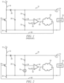
- Boost regulator 10 in FIG. 1 is one example of an SMPS topology.
- Boost regulator 10 receives an input voltage at V IN node 12, and converts the voltage to an output voltage at V OUT node 14.
- Electrical current flows through boost regulator 10 in two different paths. The first path is through inductor 18 and MOSFET 20 to ground node 24, and the second path is through inductor 18 and diode 26 to V OUT node 14.
- Electrical current flows primarily through the first path when MOSFET 20 is turned on.
- the electrical current through inductor 18 stores energy in the inductor through magnetization of a ferric core.
- the electrical current through inductor 18 reaches a fairly high magnitude because MOSFET 20 creates a substantially short circuit between V IN node 12 and ground node 24 through inductor 18.
- MOSFET 20 When a sufficient current through inductor 18 is reached, MOSFET 20 is shut off, and current flows instead through inductor 18 and diode 26 to V OUT node 14.
- the energy stored magnetically in inductor 18 during the first phase results in an electrical current through diode 26 larger than what load 16 would normally draw.
- the excess current through diode 26 raises the voltage potential at V OUT node 14 above the voltage potential of V IN node 12.
- Capacitor 28 stores electrical charge not immediately usable by load 16. As load 16 uses up the electrical energy stored in capacitor 28, the voltage potential of V OUT node 14 drops.
- MOSFET 20 turns on and off again to inject more energy through diode 26 to V OUT node 14.
- V FB V OUT ⁇ R 32 R 30 + R 32
- Comparator 40 includes a first input coupled to V FB node 34, and a second input coupled to a reference voltage at V REF node 42. Comparator 40 has an output 44 that indicates whether the voltage potential of V FB node 34 is above or below the voltage potential of V REF node 42.
- Control logic 50 receives the output signal 44 from comparator 40, and turns MOSFET 20 on and off using control signal 52 based on comparator output signal 44.
- control logic 50 will increase a switching frequency or duty cycle of control signal 52 when V FB falls below V REF .
- MOSFET 20 is switched at a predetermined frequency when V FB node 34 is below V REF node 42, and remains off when V FB node 34 is above V REF node 42.
- An engineer designing a power supply based on voltage divider feedback generally buys a controller IC with comparator 40, V REF 42, and control logic 50. Given V REF 42 set by the controller IC manufacturer, the engineer selects resistance values of resistor 30 and resistor 32 to set the voltage potential that V OUT node 14 will be regulated to. The voltage potential at V OUT node 14 will settle at a voltage indicated by equation 2.
- V OUT V REF ⁇ R 30 + R 32 R 32
- Using a resistive voltage divider for feedback creates a voltage at V FB node 34 that is acceptable for input to comparator 40.
- the resistive voltage divider is not a flexible approach.
- the voltage divider is not easily calibrated to provide high-resolution voltage control in a limited voltage range of V OUT node 14.
- the voltage divider not only reduces voltage from V OUT node 14 to V FB node 34, but also reduces the magnitude of changes in voltage. The reduction in magnitude of voltage changes from V OUT node 14 to V FB node 34 makes the control circuitry less robust against noise.
- US 4 620 179 A discloses a digital switched mode voltage regulator circuit comprising a regulation loop coupled between the output voltage of the regulator and a switch driver.
- An error signal generator comprises an analog-to-digital converter coupled to the DC output voltage through an optional voltage scaling circuit.
- US 2014/002042 A1 discloses a method for successive approximation A/D conversion.
- US 2002/125872 A1 discloses a system and method that provides virtual ripple signal generation for use in voltage regulation applications.
- FIG. 2 illustrates voltage regulator 70 with a feedback signal at V FB node 34 created by resistor 76 and current source 78 rather than a voltage divider.
- Resistor 76 and current source 78 are coupled in series between V OUT node 14 and ground node 24.
- Current source 78 draws electrical current from V OUT node 14 to ground node 24 through resistor 76.
- the current through resistor 76 results in a voltage drop from V OUT node 14 to V FB node 34 that is equivalent to the value of the resistor multiplied by the amount of current.
- Electrical current through resistor 76 can be considered equal to the value of current being drawn by current source 78 for all practical purposes, even though in practice there may be a negligible difference that may or may not be detectible.
- V OUT node 14 Due to electrical current through resistor 76 being practically a fixed value, the voltage drop across resistor 76 is also fixed.
- V OUT node 14 has a voltage potential that is above V FB node 34 by a fixed magnitude.
- the voltage potential of V FB node 34 relative to V OUT node 14 is given by equation 3, where I 78 indicates the magnitude of current source 78, and R 76 indicates the resistance value of resistor 76.
- V FB V OUT ⁇ I 78 ⁇ R 76
- V FB node 34 settles at the same voltage potential as V REF node 42 because those are the two values being input to comparator 40. Therefore, output voltage of regulator 70 at V OUT node 14 is set by configuring the magnitude by which V FB node 34 is below V OUT node 14 with the design parameters of resistor 76 and current source 78. In one embodiment, a designer of a power supply buys an integrated circuit (IC) package with comparator 40, V REF node 42, and current source 78 integrated into the package.
- IC integrated circuit
- V OUT V REF + I 78 ⁇ R 76
- the power supply designer could set the value of resistor 76 at 140 ohms to generate V OUT node 14 as a 12-volt output.
- Ohm's law dictates that the voltage drop across resistor 76 will be current (50 milliamps, set by IC manufacturer) multiplied by resistance (140 ohms, selected by the power supply designer). Therefore, the voltage across resistor 76 in the example will be 7 Volts.
- Control logic 50 will be maintaining V FB node 34 at approximately the same voltage potential as V REF node 42 (5 volts), so V OUT node 14 will be held at approximately 5 volts (the voltage of V REF ) plus 7 volts (the voltage across resistor 76), i.e., 12 volts.
- the controller IC manufacturer provides a V FB node 34 terminal on the package, which is directly coupled to current source 78 and comparator 40 within the package.
- the designer of power supply 70 selects the desired resistance value and solders resistor 76 onto a printed circuit board (PCB) or other substrate adjacent to the controller IC and electrically connected to the V FB node 34 terminal of the controller IC.
- PCB printed circuit board
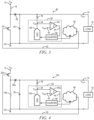
- FIG. 3 illustrates a voltage regulator 80 with a feedback circuit 82.
- Feedback circuit 82 comprises comparator 84, a counter 86, and a current-sink DAC 88.
- Comparator 84 compares V REF node 42 to V FB node 34, as above, and generates an output signal 44. The output signal 44 controls whether counter 86 increments or decrements.
- DAC 88 is a current sink that pulls current from V OUT node 14 through resistor 76, with the magnitude of current being controlled by the value stored in counter 86.
- the voltage potential at V FB node 34 is controlled by the magnitude of current being drawn by DAC 88.
- Feedback circuit 82 operates similarly to an analog-to-digital converter (ADC).
- Counter 86 provides a linear representation of the voltage potential of V OUT node 14. A digital value in counter 86 will settle at a value proportional to an analog voltage potential at V OUT node 14, and can be used to control output voltage with a purely digital controller.
- the voltage at V OUT node 14 is given by equation 5.
- counter represents the digital value stored in counter 86
- I LSB represents the change in magnitude of current drawn by DAC 88 by changing the least significant bit of the counter.
- V OUT V REF + counter ⁇ I LSB ⁇ R 76
- Comparator 84 will indicate that the V FB node 34 is at a lower voltage potential than V REF node 42, and cause counter 85 to count downward.
- the falling value in counter 86 reduces the magnitude of current drawn by DAC 88 through resistor 76, which reduces the voltage drop across the resistor.
- Counter 86 will count down until the current drawn by DAC 88 is low enough to increase the voltage of V FB node 34 to a greater value than V REF node 42.
- the amount by which the value in counter 86 falls is proportional to the drop in voltage potential at V OUT node 14.
- counter 86 moves proportionally.
- the value in counter 86 is a digital value proportional to a voltage potential at V OUT node 14.
- Control logic 90 reads the digital value in counter 86 and uses the knowledge of the output voltage to control MOSFET 20. If the value in counter 86 indicates that V OUT node 14 is at a lower than desired voltage potential, control logic 90 increases the frequency or duty cycle of switching MOSFET 20 to bring up the voltage of V OUT node 14. Control logic 90 observes the value in counter 86 to return the switching frequency to a lower value once the voltage potential at V OUT node 14 returns to the desired level.
- One advantage of utilizing a current DAC and single resistor architecture rather than a dual-resistor voltage divider is that negative voltages can be regulated by inverting the polarity of the comparator and mirroring the DAC to a source DAC rather than a sink DAC.
- the prior art architecture generally needs an additional fixed voltage for the voltage divider. Therefore, an additional pin on the controller IC is usually required to regulate negative voltages.
- Power regulator 100 in FIG. 4 is configured to regulate V OUT node 14 to a negative voltage potential.
- the polarity of diode 26 has been reversed, and the diode is labelled as diode 26a.
- the placement of inductor 18 and MOSFET 20 has been reversed, and the respective parts are labelled as 18a and 20a.
- MOSFET 20a is a P-channel device, whereas MOSFET 20 was an N-channel device.
- FIG. 4 illustrates a feedback circuit 102 with sink DAC 88 replaced with source DAC 104.
- Source DAC 104 outputs an electrical current through resistor 76 to V OUT node 14 proportional to the value in counter 86.
- a convertible DAC can be implemented that is configurable to be either a sink DAC or a source DAC, allowing a single controller IC to regulate positive or negative voltages.
- Comparator 84a is the same hardware component as comparator 84 above in some embodiments, but simply has the input polarity switched. That is, V REF node 42 is coupled to the inverting input rather than the non-inverting input of comparator 84.
- comparator 84 inputs can be controlled electronically to allow a single comparator to be configured either for regulation of positive or negative voltages.
- comparator 84 is configured for regulating negative voltages by inverting the output rather than swapping the inputs.
- V FB node 34 and V OUT node 14 of negative voltage regulator 100 in FIG. 4 are similar to the positive regulator in FIG. 3 .
- the feedback voltage is given by equation 6, and the regulated voltage is given by equation 7.
- V FB V OUT + counter ⁇ I LSB ⁇ R 76
- V OUT V REF ⁇ counter ⁇ I LSB ⁇ R 76
- Feedback circuit 102 in FIG. 4 operates in substantially the same manner as feedback circuit 82 in FIG. 3 , but is reconfigured to regulate a negative voltage instead of a positive voltage.
- FIG. 5a illustrates a power regulator 110 with feedback circuit 112.
- Feedback circuit 112 includes current-sink DAC 88 as in FIG. 3 , and a current source 114 coupled in parallel with the DAC.
- Comparator 84, counter 86, and DAC 88 operate in substantially the same manner as in FIG. 3 to populate counter 86 with a digital value proportional to the voltage potential at V OUT node 14.
- Current source 114 is coupled to V FB node 34 in parallel with current DAC 88, and draws a fixed amount of current through resistor 76 regardless of counter 86.
- Current source 114 creates a voltage potential offset because of the additional current through, and voltage drop across, resistor 76. Without current source 114, when counter 86 contains the value zero, DAC 88 draws no current and the voltage potential at V FB node 34 equals the voltage potential at V OUT node 14.
- V OUT node 14 is regulated to the voltage potential of V REF node 42, because that is the voltage potential when V FB node 34 equals V REF .
- the maximum regulated voltage potential without current source 114 is given by equation 7, with counter 86 being at the maximum value, e.g., 0xFF in hexadecimal for an 8-bit DAC.
- Line 120 in FIG. 5b illustrates an example plot of DAC 88 value on the horizontal axis versus output voltage on the vertical axis. A linear relationship is illustrated, with plot 120 beginning at the voltage potential of V REF node 42 and growing linearly as counter 86 counts from 0x00 to 0xFF.
- FIG. 5b presumes an 8-bit counter, but other bit-widths are used in other embodiments.
- the controller IC with feedback circuit 82 in FIG. 3 can be accurately regulated to voltages near V REF , which for a lot of use cases is not needed, and has relatively low maximum regulation voltages that may not be sufficient for all use cases.
- Adding current source 114 in parallel increases the voltage drop across resistor 76, and thus raises the voltage potential of V OUT node 114, for all values of counter 86.
- Plot 122 in FIG. 5b illustrates the counter 86 value versus output voltage with current source 114 added.
- V OFS indicates the difference in output voltage between a given value of counter 86 with and without current source 114.
- V OFS is given by equation 8, where I 114 is the magnitude of electrical current that current source 114 is drawing.
- V OFS I 114 ⁇ R 76 + V REF
- Adding current source 114 shifts the voltage potential at V OUT node 14 up by V OFS for a given value of counter 86, thus raising both the minimum regulable output voltage and the maximum regulable output voltage.
- the range provided by line 122 in FIG. 5b is a more useful range for many purposes. For instance, an avalanche photodiode may need a voltage in the range of 30 to 50 volts, which is totally within the vertical range of line 122, while the regulator without current source 114 only allows regulation up to say 40 volts.
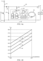
- FIG. 6a illustrates a more flexible power regulator 130, where feedback circuit 132 has a coarse DAC 134 added in parallel with DAC 88.
- Coarse DAC 134 is an adjustable current source without the same level of fine adjustment that DAC 88 offers. While an 8-bit counter 86 allows for 256 different values for the current drawn by DAC 88, coarse DAC may only have four or five different settings. In one embodiment, coarse DAC 134 is simply a plurality of current sources 114 coupled in parallel, and enablable in any combination to achieve a desired V OFS .
- FIG. 6b illustrates a plurality of possible counter 86 versus V OUT plots depending on the value selected for coarse DAC 134.
- Line 140 shows the coarse DAC sinks current equivalent to a 10 volt drop across resistor 76, allowing fine DAC 88 to adjust between 10 volts and 50 volts over V REF node 42.
- Line 142 shows coarse DAC 134 set to a 20 volt offset, allowing fine DAC 88 to adjust from 20 volts to 60 volts above V REF .
- Line 144 illustrates coarse DAC 134 with an offset of 30 volts, allowing fine DAC 88 to adjust from 30 volts to 70 volts above V REF .
- Line 146 illustrates coarse DAC 134 set to a 40 volt offset, allowing fine DAC 88 to adjust between 40 volts and 80 volts above V REF .
- additional settings of coarse DAC 134 are used to apply any desired offset to the fine adjustment range of fine DAC 88.
- Coarse DAC 134 allows the resolution of fine DAC 88 to be shifted to a desired range.
- the regulated output voltage of regulator 130 is given by equation 9.
- V OUT I 134 + I 88 ⁇ R 76 + V REF
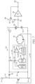
- Load 16 includes an avalanche photodiode 150 and current source 152 coupled in series between V OUT node 14 and ground node 24.
- a light signal typically delivered via a fiber optic cable, hits APD 150 and modifies the electrical resistance of the APD, which changes the voltage potential at circuit node 154.
- Transimpedance amplifier (TIA) 160 has an input coupled to circuit node 154, and an output at circuit node 162.
- a feedback path of TIA 160 comprises a MOSFET 164 and resistor 166 coupled between V DD 168 and circuit node 154.
- Semiconductor devices coupled to output node 162 receive the information from the fiber optic cable as an electrical signal.
- the APD will require that the voltage potential at V OUT node 14 fall within a different range that can vary significantly.
- the adjustment provided by coarse DAC 134 means that the fine adjustment of DAC 88 can be moved around if a particular APD 160 selected requires a different voltage range.
- the voltage of V FB node 34 always settles to be substantially equal to the voltage of V REF node 42, so any voltage range can be achieved as long as the current of coarse DAC 134 can be made high enough.
- DACs can be used for other purposes if not needed for regulator control logic.
- Many of the ICs that include the control logic may be used in situations where an external charge pump for controlling V OUT node 14 is not needed. In that case, the user can still use the DAC for other purposes.
Landscapes
- Engineering & Computer Science (AREA)
- Physics & Mathematics (AREA)
- Electromagnetism (AREA)
- General Physics & Mathematics (AREA)
- Radar, Positioning & Navigation (AREA)
- Automation & Control Theory (AREA)
- Power Engineering (AREA)
- Theoretical Computer Science (AREA)
- Dc-Dc Converters (AREA)
Claims (13)
- Procédé de fabrication d'un régulateur de tension (130), comprenant les étapes consistant à :fournir un comparateur (84) incluant une tension de référence (42) couplée à une première entrée du comparateur ;coupler une première source de courant (88) à une seconde entrée du comparateur, dans lequel la première source de courant comprend un convertisseur numérique-analogique, DAC, et dans lequel le comparateur compare une première tension à une borne de la première source de courant à la tension de référence ;coupler un compteur (86) entre une sortie du comparateur et une entrée du DAC, dans lequel la sortie du comparateur est directement couplée au compteur et un signal de sortie (44) du comparateur commande si le compteur incrémente ou décrémente ;coupler une première borne d'une résistance (76) à la seconde entrée du comparateur ;coupler un transistor (20, 20a) et une inductance (18, 18a) en série entre un noeud d'entrée de tension (12) et un noeud de tension de masse (24) ;coupler une première borne d'une diode (26, 26a) à un premier noeud de circuit entre le transistor et l'inductance ;coupler une seconde borne de la diode à la résistance au niveau d'un noeud de sortie de tension (14) ;coupler un condensateur (28) entre le noeud de tension de masse et le noeud de sortie de tension ; etfournir une logique de commande (90) couplée à une borne de commande du transistor, dans lequel la logique de commande active et désactive le transistor sur la base d'une valeur du compteur.
- Procédé selon la revendication 1, comprenant en outre le couplage de la seconde entrée du comparateur (84) au noeud de tension de masse par l'intermédiaire de la première source de courant (88).
- Procédé selon la revendication 1, dans lequel la logique de commande modifie une fréquence de commutation du transistor sur la base de la valeur du comparateur (84).
- Procédé selon la revendication 1, comprenant en outre la fourniture d'une seconde source de courant (134) couplée en parallèle avec la première source de courant (88).
- Procédé selon la revendication 4, dans lequel la première source de courant (88) est réglable de manière précise et la seconde source de courant (134) est réglable de manière grossière ; ou dans lequel la seconde source de courant (134) comprend une valeur fixe.
- Procédé selon la revendication 1, dans lequel le régulateur de tension (130) comprend une topologie de suralimentation.
- Procédé selon l'une quelconque des revendications 1 à 6, dans lequel le DAC est configurable sous forme d'un DAC collecteur ou d'un DAC source.
- Dispositif de commande de régulateur de tension (130), comprenant :un comparateur (84) comprenant une tension de référence (42) couplée à une première entrée du comparateur ;une première source de courant (88) couplée à une seconde entrée du comparateur, dans lequel la première source de courant est un convertisseur numérique-analogique, DAC, et dans lequel le comparateur est configuré pour comparer une première tension au niveau d'une borne de la première source de courant à la tension de référence ; etun compteur (86) couplé entre une sortie du comparateur et une entrée du DAC, dans lequel la sortie du comparateur est directement couplée au compteur et un signal de sortie (44) du comparateur commande si le compteur incrémente ou décrémente ;un transistor (20, 20a) et une inductance (18 ; 18a) couplés en série entre un noeud d'entrée de tension (12) et un noeud de tension de masse (24) ;une diode (26, 26a) comprenant une première borne de la diode couplée à un premier noeud de circuit entre le transistor et l'inductance ;une résistance comprenant une première borne de la résistance couplée à une seconde borne de la diode au niveau d'un noeud de sortie de tension (14) et une seconde borne de la résistance couplée à la seconde entrée du comparateur ;un condensateur (28) couplé entre le noeud de tension de masse et le noeud de sortie de tension ; etune logique de commande (90) couplée à une borne de commande du transistor et configurée pour activer et désactiver le transistor sur la base d'une valeur du compteur.
- Dispositif de commande de régulateur de tension (130) selon la revendication 8, comprenant en outre une seconde source de courant (134) couplée en parallèle avec la première source de courant (88).
- Dispositif de commande de régulateur de tension (130) selon la revendication 9, dans lequel la première source de courant (88) est réglable de manière précise et la seconde source de courant (134) est réglable de manière grossière ; ou dans lequel la seconde source de courant (134) comprend une valeur fixe
- Dispositif de commande de régulateur de tension (130) selon la revendication 8, dans lequel le noeud de tension de masse est couplé à la seconde entrée du comparateur (84) par l'intermédiaire de la première source de courant (88).
- Dispositif de commande de régulateur de tension (130) selon la revendication 8, dans lequel la logique de sortie est configurée pour modifier une fréquence de commutation du transistor sur la base de la valeur du comparateur.
- Dispositif de commande de régulateur de tension (130) selon l'une quelconque des revendications 8 à 12, dans lequel le DAC est configurable sous forme d'un DAC collecteur ou d'un DAC source.
Applications Claiming Priority (1)
| Application Number | Priority Date | Filing Date | Title |
|---|---|---|---|
| US15/958,967 US10345837B1 (en) | 2018-04-20 | 2018-04-20 | Current-based feedback control for voltage regulators |
Publications (2)
| Publication Number | Publication Date |
|---|---|
| EP3557768A1 EP3557768A1 (fr) | 2019-10-23 |
| EP3557768B1 true EP3557768B1 (fr) | 2023-09-27 |
Family
ID=66105029
Family Applications (1)
| Application Number | Title | Priority Date | Filing Date |
|---|---|---|---|
| EP19168353.1A Active EP3557768B1 (fr) | 2018-04-20 | 2019-04-10 | Commande de rétroaction basée sur le courant pour régulateurs de tension |
Country Status (3)
| Country | Link |
|---|---|
| US (1) | US10345837B1 (fr) |
| EP (1) | EP3557768B1 (fr) |
| CN (1) | CN110391734B (fr) |
Families Citing this family (4)
| Publication number | Priority date | Publication date | Assignee | Title |
|---|---|---|---|---|
| US10938403B2 (en) * | 2018-06-29 | 2021-03-02 | Texas Instruments Incorporated | Battery charging and measurement circuit |
| US11569838B2 (en) | 2020-04-09 | 2023-01-31 | Analog Devices International Unlimited Company | High efficiency current source/sink DAC |
| CN114584148B (zh) * | 2022-02-07 | 2024-06-25 | 灵矽微电子(深圳)有限责任公司 | 模数转换器及电子设备 |
| EP4318903A1 (fr) | 2022-08-02 | 2024-02-07 | Nxp B.V. | Convertisseur continu-continu à commande numérique |
Citations (1)
| Publication number | Priority date | Publication date | Assignee | Title |
|---|---|---|---|---|
| US20020125872A1 (en) * | 2001-03-12 | 2002-09-12 | Groom Terry J. | Virtual ripple generation in switch-mode power supplies |
Family Cites Families (6)
| Publication number | Priority date | Publication date | Assignee | Title |
|---|---|---|---|---|
| US4620179A (en) * | 1983-08-29 | 1986-10-28 | Harris Corporation | Method for successive approximation A/D conversion |
| US6771200B2 (en) * | 2003-04-03 | 2004-08-03 | Atmel Corporation | DAC-based voltage regulator for flash memory array |
| US9136760B2 (en) * | 2012-06-27 | 2015-09-15 | Analog Devices Global | Digital switched mode voltage regulator |
| US9219414B2 (en) * | 2013-10-28 | 2015-12-22 | Analog Devices Global | Load current readback and average estimation |
| US9755515B2 (en) * | 2015-08-04 | 2017-09-05 | Qualcomm Incorporated | Switching regulator current sensing circuits and methods |
| US10038385B2 (en) * | 2016-04-19 | 2018-07-31 | Fairchild Semiconductor Corporation | Flyback converter and controller using counter and current emulator |
-
2018
- 2018-04-20 US US15/958,967 patent/US10345837B1/en active Active
-
2019
- 2019-04-10 EP EP19168353.1A patent/EP3557768B1/fr active Active
- 2019-04-17 CN CN201910306639.5A patent/CN110391734B/zh active Active
Patent Citations (1)
| Publication number | Priority date | Publication date | Assignee | Title |
|---|---|---|---|---|
| US20020125872A1 (en) * | 2001-03-12 | 2002-09-12 | Groom Terry J. | Virtual ripple generation in switch-mode power supplies |
Also Published As
| Publication number | Publication date |
|---|---|
| CN110391734A (zh) | 2019-10-29 |
| CN110391734B (zh) | 2021-03-12 |
| EP3557768A1 (fr) | 2019-10-23 |
| US10345837B1 (en) | 2019-07-09 |
Similar Documents
| Publication | Publication Date | Title |
|---|---|---|
| EP3557768B1 (fr) | Commande de rétroaction basée sur le courant pour régulateurs de tension | |
| US9164521B2 (en) | Power supply unit, semiconductor device, and wireless communication device | |
| US8120934B2 (en) | Voltage converter and method for voltage conversion | |
| US9055646B2 (en) | Light emitting device driver circuit and control method thereof | |
| US20190052176A1 (en) | Dimmer and power converter | |
| TWI451224B (zh) | 動態電壓調整裝置及相關輸電系統 | |
| US10439390B1 (en) | Multi-port power supply apparatus and operation method thereof | |
| US9648677B2 (en) | LED driving circuit and method using single inductor | |
| TWI590574B (zh) | 電源供應裝置 | |
| US9615415B2 (en) | LED driving circuit and method using single inductor | |
| JP7018847B2 (ja) | スイッチング電源システム及び直流給電システム | |
| EP3311477B1 (fr) | Dispositif d'alimentation électrique, système d'alimentation électrique, et procédé de réglage de tension | |
| US20190013737A1 (en) | Flyback power converter circuit and primary side controller circuit thereof | |
| US10389242B2 (en) | Voltage and current sensing calibration for switching voltage regulators | |
| CN110007707B (zh) | 低压差线性稳压器及系统 | |
| US10097087B2 (en) | Power conversion including sensing a load current and adapting output voltage based on the load current | |
| US7952335B2 (en) | Power converter and method for power conversion | |
| JP2006129630A (ja) | 電源装置、および携帯機器 | |
| US12191753B2 (en) | DC-DC converter and semiconductor IC for cable voltage drop compensation | |
| TWI559812B (zh) | 定電流驅動裝置之回授裝置及回授方法 | |
| CN212433648U (zh) | 电压调整装置、芯片、电源及电子设备 | |
| KR101039992B1 (ko) | 주파수 변조 방식 및 펄스폭 변조 방식을 이용한 스위칭 모드 파워 서플라이 | |
| US20180301926A1 (en) | Tunable power supply device and parallel power supply system | |
| US20170104415A1 (en) | Switched-mode voltage converter | |
| US20140152281A1 (en) | Average inductor current mode voltage control device and method |
Legal Events
| Date | Code | Title | Description |
|---|---|---|---|
| PUAI | Public reference made under article 153(3) epc to a published international application that has entered the european phase |
Free format text: ORIGINAL CODE: 0009012 |
|
| STAA | Information on the status of an ep patent application or granted ep patent |
Free format text: STATUS: THE APPLICATION HAS BEEN PUBLISHED |
|
| AK | Designated contracting states |
Kind code of ref document: A1 Designated state(s): AL AT BE BG CH CY CZ DE DK EE ES FI FR GB GR HR HU IE IS IT LI LT LU LV MC MK MT NL NO PL PT RO RS SE SI SK SM TR |
|
| AX | Request for extension of the european patent |
Extension state: BA ME |
|
| STAA | Information on the status of an ep patent application or granted ep patent |
Free format text: STATUS: REQUEST FOR EXAMINATION WAS MADE |
|
| 17P | Request for examination filed |
Effective date: 20200422 |
|
| RBV | Designated contracting states (corrected) |
Designated state(s): AL AT BE BG CH CY CZ DE DK EE ES FI FR GB GR HR HU IE IS IT LI LT LU LV MC MK MT NL NO PL PT RO RS SE SI SK SM TR |
|
| STAA | Information on the status of an ep patent application or granted ep patent |
Free format text: STATUS: EXAMINATION IS IN PROGRESS |
|
| 17Q | First examination report despatched |
Effective date: 20211011 |
|
| 17Q | First examination report despatched |
Effective date: 20211022 |
|
| GRAP | Despatch of communication of intention to grant a patent |
Free format text: ORIGINAL CODE: EPIDOSNIGR1 |
|
| STAA | Information on the status of an ep patent application or granted ep patent |
Free format text: STATUS: GRANT OF PATENT IS INTENDED |
|
| RIC1 | Information provided on ipc code assigned before grant |
Ipc: H03M 1/68 20060101ALI20230321BHEP Ipc: H03M 1/46 20060101ALI20230321BHEP Ipc: H02M 3/157 20060101ALI20230321BHEP Ipc: H03M 1/44 20060101ALI20230321BHEP Ipc: G05F 1/575 20060101ALI20230321BHEP Ipc: G05F 1/62 20060101ALI20230321BHEP Ipc: G05F 1/563 20060101ALI20230321BHEP Ipc: H03M 1/48 20060101AFI20230321BHEP |
|
| INTG | Intention to grant announced |
Effective date: 20230412 |
|
| P01 | Opt-out of the competence of the unified patent court (upc) registered |
Effective date: 20230607 |
|
| GRAS | Grant fee paid |
Free format text: ORIGINAL CODE: EPIDOSNIGR3 |
|
| GRAA | (expected) grant |
Free format text: ORIGINAL CODE: 0009210 |
|
| STAA | Information on the status of an ep patent application or granted ep patent |
Free format text: STATUS: THE PATENT HAS BEEN GRANTED |
|
| AK | Designated contracting states |
Kind code of ref document: B1 Designated state(s): AL AT BE BG CH CY CZ DE DK EE ES FI FR GB GR HR HU IE IS IT LI LT LU LV MC MK MT NL NO PL PT RO RS SE SI SK SM TR |
|
| REG | Reference to a national code |
Ref country code: GB Ref legal event code: FG4D |
|
| REG | Reference to a national code |
Ref country code: CH Ref legal event code: EP |
|
| REG | Reference to a national code |
Ref country code: DE Ref legal event code: R096 Ref document number: 602019038046 Country of ref document: DE |
|
| REG | Reference to a national code |
Ref country code: IE Ref legal event code: FG4D |
|
| REG | Reference to a national code |
Ref country code: LT Ref legal event code: MG9D |
|
| PG25 | Lapsed in a contracting state [announced via postgrant information from national office to epo] |
Ref country code: GR Free format text: LAPSE BECAUSE OF FAILURE TO SUBMIT A TRANSLATION OF THE DESCRIPTION OR TO PAY THE FEE WITHIN THE PRESCRIBED TIME-LIMIT Effective date: 20231228 |
|
| PG25 | Lapsed in a contracting state [announced via postgrant information from national office to epo] |
Ref country code: SE Free format text: LAPSE BECAUSE OF FAILURE TO SUBMIT A TRANSLATION OF THE DESCRIPTION OR TO PAY THE FEE WITHIN THE PRESCRIBED TIME-LIMIT Effective date: 20230927 Ref country code: RS Free format text: LAPSE BECAUSE OF FAILURE TO SUBMIT A TRANSLATION OF THE DESCRIPTION OR TO PAY THE FEE WITHIN THE PRESCRIBED TIME-LIMIT Effective date: 20230927 Ref country code: NO Free format text: LAPSE BECAUSE OF FAILURE TO SUBMIT A TRANSLATION OF THE DESCRIPTION OR TO PAY THE FEE WITHIN THE PRESCRIBED TIME-LIMIT Effective date: 20231227 Ref country code: LV Free format text: LAPSE BECAUSE OF FAILURE TO SUBMIT A TRANSLATION OF THE DESCRIPTION OR TO PAY THE FEE WITHIN THE PRESCRIBED TIME-LIMIT Effective date: 20230927 Ref country code: LT Free format text: LAPSE BECAUSE OF FAILURE TO SUBMIT A TRANSLATION OF THE DESCRIPTION OR TO PAY THE FEE WITHIN THE PRESCRIBED TIME-LIMIT Effective date: 20230927 Ref country code: GR Free format text: LAPSE BECAUSE OF FAILURE TO SUBMIT A TRANSLATION OF THE DESCRIPTION OR TO PAY THE FEE WITHIN THE PRESCRIBED TIME-LIMIT Effective date: 20231228 Ref country code: FI Free format text: LAPSE BECAUSE OF FAILURE TO SUBMIT A TRANSLATION OF THE DESCRIPTION OR TO PAY THE FEE WITHIN THE PRESCRIBED TIME-LIMIT Effective date: 20230927 |
|
| REG | Reference to a national code |
Ref country code: NL Ref legal event code: MP Effective date: 20230927 |
|
| REG | Reference to a national code |
Ref country code: AT Ref legal event code: MK05 Ref document number: 1616409 Country of ref document: AT Kind code of ref document: T Effective date: 20230927 |
|
| PG25 | Lapsed in a contracting state [announced via postgrant information from national office to epo] |
Ref country code: NL Free format text: LAPSE BECAUSE OF FAILURE TO SUBMIT A TRANSLATION OF THE DESCRIPTION OR TO PAY THE FEE WITHIN THE PRESCRIBED TIME-LIMIT Effective date: 20230927 |
|
| PG25 | Lapsed in a contracting state [announced via postgrant information from national office to epo] |
Ref country code: IS Free format text: LAPSE BECAUSE OF FAILURE TO SUBMIT A TRANSLATION OF THE DESCRIPTION OR TO PAY THE FEE WITHIN THE PRESCRIBED TIME-LIMIT Effective date: 20240127 |
|
| PG25 | Lapsed in a contracting state [announced via postgrant information from national office to epo] |
Ref country code: AT Free format text: LAPSE BECAUSE OF FAILURE TO SUBMIT A TRANSLATION OF THE DESCRIPTION OR TO PAY THE FEE WITHIN THE PRESCRIBED TIME-LIMIT Effective date: 20230927 |
|
| PG25 | Lapsed in a contracting state [announced via postgrant information from national office to epo] |
Ref country code: ES Free format text: LAPSE BECAUSE OF FAILURE TO SUBMIT A TRANSLATION OF THE DESCRIPTION OR TO PAY THE FEE WITHIN THE PRESCRIBED TIME-LIMIT Effective date: 20230927 |
|
| PG25 | Lapsed in a contracting state [announced via postgrant information from national office to epo] |
Ref country code: SM Free format text: LAPSE BECAUSE OF FAILURE TO SUBMIT A TRANSLATION OF THE DESCRIPTION OR TO PAY THE FEE WITHIN THE PRESCRIBED TIME-LIMIT Effective date: 20230927 Ref country code: RO Free format text: LAPSE BECAUSE OF FAILURE TO SUBMIT A TRANSLATION OF THE DESCRIPTION OR TO PAY THE FEE WITHIN THE PRESCRIBED TIME-LIMIT Effective date: 20230927 Ref country code: IS Free format text: LAPSE BECAUSE OF FAILURE TO SUBMIT A TRANSLATION OF THE DESCRIPTION OR TO PAY THE FEE WITHIN THE PRESCRIBED TIME-LIMIT Effective date: 20240127 Ref country code: ES Free format text: LAPSE BECAUSE OF FAILURE TO SUBMIT A TRANSLATION OF THE DESCRIPTION OR TO PAY THE FEE WITHIN THE PRESCRIBED TIME-LIMIT Effective date: 20230927 Ref country code: EE Free format text: LAPSE BECAUSE OF FAILURE TO SUBMIT A TRANSLATION OF THE DESCRIPTION OR TO PAY THE FEE WITHIN THE PRESCRIBED TIME-LIMIT Effective date: 20230927 Ref country code: CZ Free format text: LAPSE BECAUSE OF FAILURE TO SUBMIT A TRANSLATION OF THE DESCRIPTION OR TO PAY THE FEE WITHIN THE PRESCRIBED TIME-LIMIT Effective date: 20230927 Ref country code: AT Free format text: LAPSE BECAUSE OF FAILURE TO SUBMIT A TRANSLATION OF THE DESCRIPTION OR TO PAY THE FEE WITHIN THE PRESCRIBED TIME-LIMIT Effective date: 20230927 Ref country code: PT Free format text: LAPSE BECAUSE OF FAILURE TO SUBMIT A TRANSLATION OF THE DESCRIPTION OR TO PAY THE FEE WITHIN THE PRESCRIBED TIME-LIMIT Effective date: 20240129 Ref country code: SK Free format text: LAPSE BECAUSE OF FAILURE TO SUBMIT A TRANSLATION OF THE DESCRIPTION OR TO PAY THE FEE WITHIN THE PRESCRIBED TIME-LIMIT Effective date: 20230927 |
|
| PG25 | Lapsed in a contracting state [announced via postgrant information from national office to epo] |
Ref country code: PL Free format text: LAPSE BECAUSE OF FAILURE TO SUBMIT A TRANSLATION OF THE DESCRIPTION OR TO PAY THE FEE WITHIN THE PRESCRIBED TIME-LIMIT Effective date: 20230927 Ref country code: IT Free format text: LAPSE BECAUSE OF FAILURE TO SUBMIT A TRANSLATION OF THE DESCRIPTION OR TO PAY THE FEE WITHIN THE PRESCRIBED TIME-LIMIT Effective date: 20230927 |
|
| REG | Reference to a national code |
Ref country code: DE Ref legal event code: R097 Ref document number: 602019038046 Country of ref document: DE |
|
| PG25 | Lapsed in a contracting state [announced via postgrant information from national office to epo] |
Ref country code: DK Free format text: LAPSE BECAUSE OF FAILURE TO SUBMIT A TRANSLATION OF THE DESCRIPTION OR TO PAY THE FEE WITHIN THE PRESCRIBED TIME-LIMIT Effective date: 20230927 |
|
| PG25 | Lapsed in a contracting state [announced via postgrant information from national office to epo] |
Ref country code: DK Free format text: LAPSE BECAUSE OF FAILURE TO SUBMIT A TRANSLATION OF THE DESCRIPTION OR TO PAY THE FEE WITHIN THE PRESCRIBED TIME-LIMIT Effective date: 20230927 |
|
| PLBE | No opposition filed within time limit |
Free format text: ORIGINAL CODE: 0009261 |
|
| STAA | Information on the status of an ep patent application or granted ep patent |
Free format text: STATUS: NO OPPOSITION FILED WITHIN TIME LIMIT |
|
| 26N | No opposition filed |
Effective date: 20240628 |
|
| PG25 | Lapsed in a contracting state [announced via postgrant information from national office to epo] |
Ref country code: SI Free format text: LAPSE BECAUSE OF FAILURE TO SUBMIT A TRANSLATION OF THE DESCRIPTION OR TO PAY THE FEE WITHIN THE PRESCRIBED TIME-LIMIT Effective date: 20230927 |
|
| PG25 | Lapsed in a contracting state [announced via postgrant information from national office to epo] |
Ref country code: SI Free format text: LAPSE BECAUSE OF FAILURE TO SUBMIT A TRANSLATION OF THE DESCRIPTION OR TO PAY THE FEE WITHIN THE PRESCRIBED TIME-LIMIT Effective date: 20230927 |
|
| PG25 | Lapsed in a contracting state [announced via postgrant information from national office to epo] |
Ref country code: BG Free format text: LAPSE BECAUSE OF FAILURE TO SUBMIT A TRANSLATION OF THE DESCRIPTION OR TO PAY THE FEE WITHIN THE PRESCRIBED TIME-LIMIT Effective date: 20230927 |
|
| PG25 | Lapsed in a contracting state [announced via postgrant information from national office to epo] |
Ref country code: MC Free format text: LAPSE BECAUSE OF FAILURE TO SUBMIT A TRANSLATION OF THE DESCRIPTION OR TO PAY THE FEE WITHIN THE PRESCRIBED TIME-LIMIT Effective date: 20230927 |
|
| PG25 | Lapsed in a contracting state [announced via postgrant information from national office to epo] |
Ref country code: MC Free format text: LAPSE BECAUSE OF FAILURE TO SUBMIT A TRANSLATION OF THE DESCRIPTION OR TO PAY THE FEE WITHIN THE PRESCRIBED TIME-LIMIT Effective date: 20230927 Ref country code: BG Free format text: LAPSE BECAUSE OF FAILURE TO SUBMIT A TRANSLATION OF THE DESCRIPTION OR TO PAY THE FEE WITHIN THE PRESCRIBED TIME-LIMIT Effective date: 20230927 |
|
| REG | Reference to a national code |
Ref country code: CH Ref legal event code: PL |
|
| PG25 | Lapsed in a contracting state [announced via postgrant information from national office to epo] |
Ref country code: LU Free format text: LAPSE BECAUSE OF NON-PAYMENT OF DUE FEES Effective date: 20240410 |
|
| REG | Reference to a national code |
Ref country code: BE Ref legal event code: MM Effective date: 20240430 |
|
| PG25 | Lapsed in a contracting state [announced via postgrant information from national office to epo] |
Ref country code: LU Free format text: LAPSE BECAUSE OF NON-PAYMENT OF DUE FEES Effective date: 20240410 |
|
| PG25 | Lapsed in a contracting state [announced via postgrant information from national office to epo] |
Ref country code: BE Free format text: LAPSE BECAUSE OF NON-PAYMENT OF DUE FEES Effective date: 20240430 |
|
| PG25 | Lapsed in a contracting state [announced via postgrant information from national office to epo] |
Ref country code: BE Free format text: LAPSE BECAUSE OF NON-PAYMENT OF DUE FEES Effective date: 20240430 Ref country code: CH Free format text: LAPSE BECAUSE OF NON-PAYMENT OF DUE FEES Effective date: 20240430 |
|
| PG25 | Lapsed in a contracting state [announced via postgrant information from national office to epo] |
Ref country code: HR Free format text: LAPSE BECAUSE OF FAILURE TO SUBMIT A TRANSLATION OF THE DESCRIPTION OR TO PAY THE FEE WITHIN THE PRESCRIBED TIME-LIMIT Effective date: 20230927 |
|
| PG25 | Lapsed in a contracting state [announced via postgrant information from national office to epo] |
Ref country code: IE Free format text: LAPSE BECAUSE OF NON-PAYMENT OF DUE FEES Effective date: 20240410 |
|
| PGFP | Annual fee paid to national office [announced via postgrant information from national office to epo] |
Ref country code: DE Payment date: 20250429 Year of fee payment: 7 |
|
| PGFP | Annual fee paid to national office [announced via postgrant information from national office to epo] |
Ref country code: GB Payment date: 20250428 Year of fee payment: 7 |
|
| PGFP | Annual fee paid to national office [announced via postgrant information from national office to epo] |
Ref country code: FR Payment date: 20250425 Year of fee payment: 7 |
|
| PG25 | Lapsed in a contracting state [announced via postgrant information from national office to epo] |
Ref country code: CY Free format text: LAPSE BECAUSE OF FAILURE TO SUBMIT A TRANSLATION OF THE DESCRIPTION OR TO PAY THE FEE WITHIN THE PRESCRIBED TIME-LIMIT; INVALID AB INITIO Effective date: 20190410 |
|
| PG25 | Lapsed in a contracting state [announced via postgrant information from national office to epo] |
Ref country code: HU Free format text: LAPSE BECAUSE OF FAILURE TO SUBMIT A TRANSLATION OF THE DESCRIPTION OR TO PAY THE FEE WITHIN THE PRESCRIBED TIME-LIMIT; INVALID AB INITIO Effective date: 20190410 |