EP3557564A1 - Panneaux d'affichage électroniques - Google Patents
Panneaux d'affichage électroniques Download PDFInfo
- Publication number
- EP3557564A1 EP3557564A1 EP19167437.3A EP19167437A EP3557564A1 EP 3557564 A1 EP3557564 A1 EP 3557564A1 EP 19167437 A EP19167437 A EP 19167437A EP 3557564 A1 EP3557564 A1 EP 3557564A1
- Authority
- EP
- European Patent Office
- Prior art keywords
- edge
- light
- display panel
- region
- emitting elements
- Prior art date
- Legal status (The legal status is an assumption and is not a legal conclusion. Google has not performed a legal analysis and makes no representation as to the accuracy of the status listed.)
- Withdrawn
Links
Images



Classifications
-
- G—PHYSICS
- G09—EDUCATION; CRYPTOGRAPHY; DISPLAY; ADVERTISING; SEALS
- G09G—ARRANGEMENTS OR CIRCUITS FOR CONTROL OF INDICATING DEVICES USING STATIC MEANS TO PRESENT VARIABLE INFORMATION
- G09G3/00—Control arrangements or circuits, of interest only in connection with visual indicators other than cathode-ray tubes
- G09G3/006—Electronic inspection or testing of displays and display drivers, e.g. of LED or LCD displays
-
- G—PHYSICS
- G09—EDUCATION; CRYPTOGRAPHY; DISPLAY; ADVERTISING; SEALS
- G09G—ARRANGEMENTS OR CIRCUITS FOR CONTROL OF INDICATING DEVICES USING STATIC MEANS TO PRESENT VARIABLE INFORMATION
- G09G3/00—Control arrangements or circuits, of interest only in connection with visual indicators other than cathode-ray tubes
- G09G3/20—Control arrangements or circuits, of interest only in connection with visual indicators other than cathode-ray tubes for presentation of an assembly of a number of characters, e.g. a page, by composing the assembly by combination of individual elements arranged in a matrix no fixed position being assigned to or needed to be assigned to the individual characters or partial characters
- G09G3/22—Control arrangements or circuits, of interest only in connection with visual indicators other than cathode-ray tubes for presentation of an assembly of a number of characters, e.g. a page, by composing the assembly by combination of individual elements arranged in a matrix no fixed position being assigned to or needed to be assigned to the individual characters or partial characters using controlled light sources
- G09G3/30—Control arrangements or circuits, of interest only in connection with visual indicators other than cathode-ray tubes for presentation of an assembly of a number of characters, e.g. a page, by composing the assembly by combination of individual elements arranged in a matrix no fixed position being assigned to or needed to be assigned to the individual characters or partial characters using controlled light sources using electroluminescent panels
- G09G3/32—Control arrangements or circuits, of interest only in connection with visual indicators other than cathode-ray tubes for presentation of an assembly of a number of characters, e.g. a page, by composing the assembly by combination of individual elements arranged in a matrix no fixed position being assigned to or needed to be assigned to the individual characters or partial characters using controlled light sources using electroluminescent panels semiconductive, e.g. using light-emitting diodes [LED]
-
- G—PHYSICS
- G09—EDUCATION; CRYPTOGRAPHY; DISPLAY; ADVERTISING; SEALS
- G09G—ARRANGEMENTS OR CIRCUITS FOR CONTROL OF INDICATING DEVICES USING STATIC MEANS TO PRESENT VARIABLE INFORMATION
- G09G3/00—Control arrangements or circuits, of interest only in connection with visual indicators other than cathode-ray tubes
- G09G3/20—Control arrangements or circuits, of interest only in connection with visual indicators other than cathode-ray tubes for presentation of an assembly of a number of characters, e.g. a page, by composing the assembly by combination of individual elements arranged in a matrix no fixed position being assigned to or needed to be assigned to the individual characters or partial characters
- G09G3/34—Control arrangements or circuits, of interest only in connection with visual indicators other than cathode-ray tubes for presentation of an assembly of a number of characters, e.g. a page, by composing the assembly by combination of individual elements arranged in a matrix no fixed position being assigned to or needed to be assigned to the individual characters or partial characters by control of light from an independent source
- G09G3/36—Control arrangements or circuits, of interest only in connection with visual indicators other than cathode-ray tubes for presentation of an assembly of a number of characters, e.g. a page, by composing the assembly by combination of individual elements arranged in a matrix no fixed position being assigned to or needed to be assigned to the individual characters or partial characters by control of light from an independent source using liquid crystals
-
- G—PHYSICS
- G09—EDUCATION; CRYPTOGRAPHY; DISPLAY; ADVERTISING; SEALS
- G09G—ARRANGEMENTS OR CIRCUITS FOR CONTROL OF INDICATING DEVICES USING STATIC MEANS TO PRESENT VARIABLE INFORMATION
- G09G2300/00—Aspects of the constitution of display devices
- G09G2300/02—Composition of display devices
- G09G2300/026—Video wall, i.e. juxtaposition of a plurality of screens to create a display screen of bigger dimensions
-
- G—PHYSICS
- G09—EDUCATION; CRYPTOGRAPHY; DISPLAY; ADVERTISING; SEALS
- G09G—ARRANGEMENTS OR CIRCUITS FOR CONTROL OF INDICATING DEVICES USING STATIC MEANS TO PRESENT VARIABLE INFORMATION
- G09G2300/00—Aspects of the constitution of display devices
- G09G2300/04—Structural and physical details of display devices
- G09G2300/0421—Structural details of the set of electrodes
-
- G—PHYSICS
- G09—EDUCATION; CRYPTOGRAPHY; DISPLAY; ADVERTISING; SEALS
- G09G—ARRANGEMENTS OR CIRCUITS FOR CONTROL OF INDICATING DEVICES USING STATIC MEANS TO PRESENT VARIABLE INFORMATION
- G09G2310/00—Command of the display device
- G09G2310/02—Addressing, scanning or driving the display screen or processing steps related thereto
- G09G2310/0202—Addressing of scan or signal lines
- G09G2310/0221—Addressing of scan or signal lines with use of split matrices
-
- G—PHYSICS
- G09—EDUCATION; CRYPTOGRAPHY; DISPLAY; ADVERTISING; SEALS
- G09G—ARRANGEMENTS OR CIRCUITS FOR CONTROL OF INDICATING DEVICES USING STATIC MEANS TO PRESENT VARIABLE INFORMATION
- G09G2310/00—Command of the display device
- G09G2310/02—Addressing, scanning or driving the display screen or processing steps related thereto
- G09G2310/0232—Special driving of display border areas
-
- G—PHYSICS
- G09—EDUCATION; CRYPTOGRAPHY; DISPLAY; ADVERTISING; SEALS
- G09G—ARRANGEMENTS OR CIRCUITS FOR CONTROL OF INDICATING DEVICES USING STATIC MEANS TO PRESENT VARIABLE INFORMATION
- G09G2320/00—Control of display operating conditions
- G09G2320/02—Improving the quality of display appearance
- G09G2320/0233—Improving the luminance or brightness uniformity across the screen
-
- G—PHYSICS
- G09—EDUCATION; CRYPTOGRAPHY; DISPLAY; ADVERTISING; SEALS
- G09G—ARRANGEMENTS OR CIRCUITS FOR CONTROL OF INDICATING DEVICES USING STATIC MEANS TO PRESENT VARIABLE INFORMATION
- G09G2320/00—Control of display operating conditions
- G09G2320/02—Improving the quality of display appearance
- G09G2320/0242—Compensation of deficiencies in the appearance of colours
-
- G—PHYSICS
- G09—EDUCATION; CRYPTOGRAPHY; DISPLAY; ADVERTISING; SEALS
- G09G—ARRANGEMENTS OR CIRCUITS FOR CONTROL OF INDICATING DEVICES USING STATIC MEANS TO PRESENT VARIABLE INFORMATION
- G09G2320/00—Control of display operating conditions
- G09G2320/06—Adjustment of display parameters
- G09G2320/0626—Adjustment of display parameters for control of overall brightness
-
- G—PHYSICS
- G09—EDUCATION; CRYPTOGRAPHY; DISPLAY; ADVERTISING; SEALS
- G09G—ARRANGEMENTS OR CIRCUITS FOR CONTROL OF INDICATING DEVICES USING STATIC MEANS TO PRESENT VARIABLE INFORMATION
- G09G3/00—Control arrangements or circuits, of interest only in connection with visual indicators other than cathode-ray tubes
- G09G3/20—Control arrangements or circuits, of interest only in connection with visual indicators other than cathode-ray tubes for presentation of an assembly of a number of characters, e.g. a page, by composing the assembly by combination of individual elements arranged in a matrix no fixed position being assigned to or needed to be assigned to the individual characters or partial characters
Definitions
- the present disclosure relates to an electronic apparatus, and in particular to an electronic apparatus having a display panel.
- a plurality of display screens are connected into one screen wall to display large-area advertisements.
- each display screen may experience a processing error during production.
- the images displayed on two adjacent display screens may have differences in brightness or chromaticity, which diminishes the quality of the integrated image.
- the electronic apparatus of the present disclosure may improve the quality of the integrated image by connecting display panels with small differences in brightness and chromaticity.
- the present disclosure provides an electronic apparatus that includes a first display panel and a second display panel.
- the first display panel includes a plurality of first light-emitting elements, a first edge, and a first left region.
- the second display panel includes a plurality of second light-emitting elements, a second edge, and a first right region. The second edge adjacent to the first edge.
- the difference between the average brightness of the first light-emitting elements in the first left region and the average brightness of the second light-emitting elements in the first right region is in a range from 0% to 20%.
- first and second features are formed in direct contact
- additional features may be formed between the first and second features, such that the first and second features may not be in direct contact
- Fig. 1 is a perspective view of the electronic apparatus 1 in accordance with some embodiments of the present disclosure.
- the electronic apparatus 1 may be a television wall.
- the electronic apparatus 1 includes a housing 10 and display panels 20.
- the display panel 20 may be arranged on the housing 10 in an array.
- the display panels 20 may be arranged on the same plane, and the size of the display panels 20may be the same.
- the shape of the display panels 20 may be the same or substantially the same.
- the display panels 20 may be rectangular.
- the display panels 20 of the present disclosure are not limited to the same size or shape, as long as the display panels 20 that can be combined and the display signals of the display panels 20 that can be connected to each other. In other words, the size and/or shape of each display panel 20 may vary.
- the number of the display panels 20 may be two or more.
- the number of the display panels 20 may be two, four, six, nine, twelve, or sixteen, but it is not limited thereto.
- the number of display panel 20 is 4.
- Each display panel 20 can be used to display an image.
- the image displayed by each display panel 20 can be connected to an integrated image.
- the display panel 20 may be a light-emitting diode panel, a quantum dot panel or a liquid-crystal panel.
- the present disclosure does not particularly limit the type of the display panel, as long as the image can be displayed.
- the display panel 20 may be a self-illuminating panel, such as a light-emitting diode panel, and a quantum dot panel.
- the display panel 20 includes light-emitting elements 21.
- the light-emitting elements 21 may be arranged in an array on the display panel 20, and each light-emitting element 21 may be separated from each other.
- each light-emitting element 21 corresponds to a pixel or a sub-pixel of the integrated image.
- the display panel 20 may be liquid-crystal-display (LCD) panel, and the light-emitting elements 21 are the opening regions of the pixels or sub-pixels.
- the opening regions of the pixels allow the backlight in the display panel 20 to pass through, so as to display the image.
- the size of the light-emitting elements 21 is enlarged in the drawings of the present disclosure and the number of light-emitting elements 21 is reduced.
- the number of light-emitting elements 21 of each display panel 20 may be in a range from one thousand to thirty million, but it is not limited thereto.
- Each light-emitting element 21 includes light-emitting units 22.
- the light-emitting units 22 may be arranged in an array. In the embodiment, each light-emitting element 21 has four light-emitting units 22, but it is not limited thereto.
- the distance of two adjacent light-emitting units 22 in one of the light-emitting elements 21 is less than the distance of two light-emitting units 22 respectively in two adjacent light-emitting elements 21.
- two adjacent light-emitting units 22 may be connected to each other.
- the light-emitting units 22 may be light-emitting diodes. Each light-emitting unit 22 is configured to emit a Light of a specific color. For example, red light-emitting units 22 are configured to emit red light. Green light-emitting units 22 are configured to emit green light. Blue light-emitting units 22 are configured to emit blue light. In the embodiment, each light-emitting element 21 has at least three colors of light-emitting units 22.
- the light-emitting units 22 of the same color on each display panel 20 may emit different chromaticity and brightness due to manufacturing errors.
- the difference in color and brightness between two adjacent display panels 20 should be within a predetermined value, which is described in detail below.
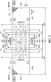
- Fig. 2 is a schematic view of the display panel 20 in accordance with some embodiments of the present disclosure.
- two display panels 20 arranged on the same plane are drawn in Fig. 2 .
- a few light-emitting elements 21 are drawn in each display panel 20.
- the light-emitting elements 21 should be properly distributed on the display panels 20 as shown in Fig. 1 .
- the display panel (second display panel) 20b are arranged on the right side of the display panel (first display panel) 20a.
- the position of the display panel 20b relative to the display panel 20a in Fig. 2 is only an example, and the position of the display panel 20b relative to the display panel 20a should not be limited to the position in Fig. 2 .
- the display panel 20b can be arranged on the left side, upper side or lower side of the display panel 20a.
- the display panel 20a may be rectangular, but it is not limited thereto.
- the display panel 20a has an edge (first edge) E11, an edge E12, an edge E13, and an edge E14.
- Edge E11 is opposite to edge E12.
- Edge E11 and edge E12 extend in the first direction D1.
- edge E11 is parallel to edge E12.
- the length of edge E11 may be substantially equal to the length of edge E12.
- edge E11 and edge E12 may not be parallel and they may have different lengths.
- Edge E11 and edge E12 are connected to edge E13 and edge E14.
- edge E11 and edge E12 are perpendicular to edge E13 and edge E14.
- Edge E13 is opposite to edge E14.
- Edge E13 and edge E14 extend in the second direction D2.
- the second direction D2 may be perpendicular to the first direction D1.
- edge E13 may be parallel to edge E14.
- the length of edge E13 may be substantially equal to the length of edge E14.
- the present disclosure does not particularly limit whether the edges are parallel or whether they are the same length. In the irregular display panel, edge E13 may not be parallel to edge E14 and have a different length than edge E14.
- the display panel 20b may be rectangular, but it is not limited thereto.
- the display panel 20b may be polygonal.
- the display panel 20b has an edge (second edge) E21, an edge E22, an edge E23, and an edge E24.
- Edge E21 is opposite to edge E22.
- Edge E21 and edge E22 extend in the first direction D1. In other words, edge E21 may parallel to edge E22.
- the length of edge E21 may be substantially equal to the length of edge E22.
- Edge E21 and edge E22 are connected to edge E23 and edge E24. In some embodiments, edge E21 and edge E22 may be perpendicular to edge E23 and edge E24. Edge E23 is opposite to edge E24. Edge E23 and edge E24 extend in the second direction D2. In other words, edge E23 is parallel to edge E24. The length of edge E23 is substantially equal to the length of edge E24.
- edge E11 is adjacent to or in contact with edge E21.
- Edge E11 may be parallel to edge E21.
- the length of edge E11 may be substantially equal to the length of edge E21.
- the lengths of edge E11, edge E12, edge E21 and edge E22 are less than the lengths of edge E13, edge E14, edge E23 and edge E24.
- the lengths of edge E11, edge E12, edge E21 and edge E22 are greater than the lengths of edge E13, edge E14, edge E23, and edge E24.
- the display panel 20a has a first left region Z11, a second left region Z12, a third left region Z13, a fourth left region Z14, and a fifth left region Z15.
- the display panel 20a includes light-emitting elements (first light-emitting elements) 21a.
- the light-emitting elements 21a are suitably distributed in the display panel 20a, and are located in the first left region Z11, the second left region Z12, the third left region Z13, the fourth left region Z14, and the fifth left region Z15.
- the first left region Z11 is a region between the edge E11 and a boundary (first boundary) T11 parallel to the edge E11.
- the distance d11 between the boundary T11 and the edge E11 is about one-half of the width or the length of the display panel 20a.
- the boundary is defined as a line that is parallel to the edges E11 and E21 of two adjacent display panels 20 or a curve with a shape that is substantially the same as the edges E11 and E21 of two adjacent display panels 20.
- the distance between the boundary and the edge (E11 or E12) is defined as a perpendicular distance between the lines or the maximum distance between two curves.
- the distance between the boundary T11 and the edge E11 corresponds to the length of the display panel 20.
- the distance d11 between the boundary T11 and the edge E11 may be substantially equal to one-half of the length of display panel 20a. Moreover, the distance d11 between the boundary T11 and edge E11 may be substantially equal to one-half of the distance d16 between edge E11 and edge E12.
- the width or length of the display panel 20a is measured in a direction that is perpendicular to the edge E11. In the embodiment, distance d16 and distance d11 are measured in substantially the same direction.
- the second left region Z12 is a region between the edge E11 and a boundary (second boundary) T12 parallel to the edge E11.
- the area of the second left region Z12 is less than the area of the first left region Z11. In the embodiment, the area of the second left region Z12 is less than or equal to two-thirds the area of the first left region Z11.
- the distance d12 between the boundary T12 and the edge E11 may be substantially equal to one-third the length of the display panel 20a. In the embodiment, the distance d12 between the boundary T12 and the edge E11 may be substantially equal to one-third the length of the display panel 20a. In other words, the distance d12 between the boundary T12 and edge E11 may be substantially equal to one-third the distance d16 between edge E11 and edge E12.
- the third left region Z13 is a region between the edge E11 and a boundary (third boundary) T13 parallel to the edge E11.
- the area of the third left region Z13 is less than the area of the second left region Z12. In the embodiment, the area of the third left region Z13 is less than or equal to three-quarters the area of the second left region Z12.
- the distance d13 between the boundary T13 and the edge E11 may be substantially equal to one-quarter the length of the display panel 20a. In the embodiment, the distance d13 between the boundary T13 and the edge E11 may be substantially equal to one-quarter the length of the display panel 20a. In other words, the distance d13 between the boundary T13 and the edge E11 may be substantially equal to one-quarter the distance d16 between the edge E11 and the edge E12.
- the fourth left region Z14 is a region between the edge E11 and a boundary T14 parallel to the edge E11.
- the area of the fourth left region Z14 is less than the area of the third left region Z13.
- the area of the fourth left region Z14 is less than or equal to four-fifths the area of the third left region Z13.
- the distance d14 between the boundary T14 and the edge E11 may be substantially equal to one-fifth the length of the display panel 20a. In the embodiment, the distance d14 between the boundary T14 and the edge E11 may be substantially equal to one-fifth the length of the display panel 20a. In other words, the distance d14 between the boundary T14 and the edge E11 may be substantially equal to one-fifth the distance d16 of the edge E11 and the edge E12.
- the fifth left region Z15 is a region between the edge E11 and a boundary T15 parallel to the edge E11.
- the area of the fifth left region Z15 is less than the area of the fourth left region Z14. In the embodiment, the area of the fifth left region Z15 is less than or equal to one-half the area of the fourth left region Z14.
- the distance d15 between the boundary T15 and the edge E11 may be substantially equal to one-tenth the length of the display panel 20a. In the embodiment, the distance d15 between the boundary T15 and the edge E11 may be substantially equal to one-tenth the length of the display panel 20a. In other words, the distance d15 between the boundary T15 and the edge E11 may be substantially equal to one-tenth the distance d16 between the edge E11 and the edge E12.
- the display panel 20b has a first right region Z21, a second right region Z22, a third right region Z23, a fourth right region Z24, and a fifth right region Z25.
- the display panel 20b includes light-emitting elements (second light-emitting elements) 21b.
- the light-emitting elements 21b are suitably distributed in the display panel 20b, and are located in the first right region Z21, the second right region Z22, the third right region Z23, the fourth right region Z24, and the fifth right region Z25.
- the first right region Z21 is a region between the edge E21 and a boundary (first boundary) T21 parallel to the edge E21.
- the distance d21 between the boundary T21 and the edge E21 may be equal to one-half of the length of display panel 20b.
- the distance d21 between the boundary T21 and the edge E21 may be substantially equal to one-half the distance d26 between the edge E21 and the edge E22.
- the distance d21 between the boundary T21 and the edge E21 may be substantially equal to one-half the distance d26 between the edge E21 and the edge E22.
- the distance d26 may be the length of the display panel 20b. In the embodiment, the distance d26 and the distance d21 are measured in substantially the same direction.
- the second right region Z22 is a region between the edge E21 and a boundary T22 parallel to the edge E21.
- the area of the second right region Z22 is less than the area of the first right region Z21. In the embodiment, the area of the second right region Z22 is less than or equal to two-thirds the area of the first right region Z21.
- the distance d22 between the boundary T22 and the edge E21 may be substantially equal to one-third the length of the display panel 20b. In the embodiment, the distance d22 between the boundary T22 and the edge E21 may be substantially equal to one-third the length of the display panel 20b. In other words, the distance d22 between the boundary T22 and the edge E21 may be substantially equal to one-third the distance d26 between edge E21 and edge E22.
- the third right region Z23 is a region between the edge E21 and a boundary T23 parallel to the edge E21.
- the area of the third right region Z23 is less than the area of the second right region Z22. In the embodiment, the area of the third right region Z23 is less than or equal to three-quarters the area of the second right region Z22.
- the distance d23 between the boundary T23 and the edge E21 may be substantially equal to one-quarter the length of the display panel 20b. In the embodiment, the distance d23 between the boundary T23 and the edge E21 may be substantially equal to one-quarter the length of the display panel 20b. In other words, the distance d23 between the boundary T23 and the edge E21 may be substantially equal to one-quarter the distance d26 between the edge E21 and the edge E22.
- the fourth right region Z24 is a region between the edge E21 and a boundary T24 parallel to the edge E21.
- the area of the fourth right region Z24 is less than the area of the third right region Z23. In the embodiment, the area of the fourth right region Z24 is less than or equal to four-fifths the area of the third right region Z23.
- the distance d24 between the boundary T24 and the edge E21 may be substantially equal to one-fifth the length of the display panel 20b. In the embodiment, the distance d24 between the boundary T24 and the edge E21 may be substantially equal to one-fifth the length of the display panel 20b. In other words, the distance d24 between the boundary T24 and edge E21 may be substantially equal to one-fifth the distance d26 of edge E21 and edge E22.
- the fifth right region Z25 is a region between the edge E21 and a boundary T25 parallel to the edge E21.
- the area of the fifth right region Z25 is less than the area of the fourth right region Z24. In the embodiment, the area of the fifth right region Z25 is less than or equal to one-half the area of the fourth right region Z24.
- the distance d25 between the boundary T25 and the edge E21 may be substantially equal to one-tenth the length of the display panel 20b. In the embodiment, the distance d25 between the boundary T25 and the edge E21 may be substantially equal to one-tenth the length of the display panel 20b. In other words, the distance d25 between the boundary T25 and edge E21 may be substantially equal to one-tenth the distance d26 between edge E21 and edge E22.
- the area of the first left region Z11 is substantially equal to the area of the first right region Z21.
- the area of the second left region Z12 is substantially equal to the area of the second right region Z22.
- the area of the third left region Z13 is substantially equal to the area of the third right region Z23.
- the area of the fourth left region Z14 is substantially equal to the area of the fourth right region Z24.
- the area of the fifth left region Z15 is substantially equal to the area of the fifth right region Z25.
- the difference between the average brightness of the first light-emitting units 22a in the first left region Z11 and the average brightness of the second light-emitting units 22b in the first right region Z21 is in a range from 0% to 20%.
- the difference between the average brightness of the first light-emitting units 22a located in the second left region Z12 and the average brightness of the second light-emitting units 22b located in the second right region Z22 is in a range from 0% to 14%.
- the measurement of the average brightness may be measured using a CA-210 (Display color analysis), or may be measured using other suitable instruments, but the present disclosure is not particularly limited thereto.
- the difference between the average brightness of the first light-emitting units 22a in the third left region Z13 and the average brightness of the second light-emitting units 22b in the third right region Z23 is in a range from 0% to 10%.
- the difference between the average brightness of the first light-emitting units 22a in the fourth left region Z14 and the average brightness of the second light-emitting units 22b in the fourth right region Z24 is in a range from 0% to 7%.
- the difference between the average brightness of the first light-emitting units 22a in the fifth region Z15 and the average brightness of the second light-emitting units 22b in the fifth region z25 is in a range from 0% to 5%.
- At least three test regions are selected in each region, and the brightness of light-emitting units 22 in the test regions are detected.
- the average brightness is obtained by averaging the brightness of the test regions.
- all light-emitting units 22 in the display panel 20 can be activated, and light-emitting units 22 are provided with the appropriate voltage, current or power.
- test regions may be close to edges E13 and E23, close to edges E14 and E24, close to regions between edge E13 and edge E14, and/or regions between edge E23 and edge E24.
- the brightness of light-emitting units (first light-emitting units) 22a in at least three first test regions S1 in the first left region Z11 is detected and averaged, so as to obtain the average brightness of the light-emitting units 22a located in the first left region Z11.
- the brightness of light-emitting units (second light-emitting units) 22b in at least three first test regions S1 in the first right region Z21 is detected and averaged, so as to obtain the average brightness of the light-emitting units 22b located in the first right region Z21.
- the first test region S1 may not be located in the second left region Z12 and the second right region Z22.
- the brightness of light-emitting units 22a in at least three second test regions S2 in the second left region Z12 is detected and averaged, so as to obtain the average brightness of the light-emitting units 22a located in the second left region Z12.
- the brightness of light-emitting units 22b in at least three second test regions S2 in the second right region Z22 is detected and averaged, so as to obtain, and the average brightness of the light-emitting units 22b located in the second right region Z22.
- the second test region S2 may not be located in the third left region Z13 or the third right region Z23.
- the brightness of light-emitting units 22a in at least three third test regions S3 in the third left region Z13 is detected and averaged, so as to obtain the average brightness of the light-emitting units 22a located in the third left region Z13.
- the brightness of light-emitting units 22b in at least three third test regions S3 in the third right region Z23 is detected and averaged, so as to obtain the average brightness of the light-emitting units 22b located in the third right region Z23.
- the third right region Z23 may not be located in the fourth left region Z14 or the fourth right region Z24.
- the brightness of light-emitting units 22a in at least three fourth test regions S4 in the fourth left region Z14 is detected and averaged, so as to obtain the average brightness of the light-emitting units 22a located in the fourth left region Z14.
- the brightness of light-emitting units 22b in at least three fourth test regions S4 in the fourth right region Z24 is detected and averaged, so as to obtain the average brightness of the light-emitting units 22b located in the fourth right region Z24.
- the fourth right region Z24 may not be located in the fifth left region Z15 or the fifth right region Z25.
- the brightness of light-emitting units 22a in at least three fifth test regions S5 in the fifth left region Z15 is detected and averaged, so as to obtain the average brightness of the light-emitting units 22a located in the fifth left region Z15.
- the brightness of light-emitting units 22b in at least three fifth test regions S5 in the fifth left region Z15 is detected and averaged, so as to obtain the average brightness of the light-emitting units 22b located in the fifth right region Z25.
- the absolute value of the difference between the X-axis chromaticity coordinate (or the Y-axis chromaticity coordinate) of the light-emitting units 22a located in the first left region Z11 and the X-axis chromaticity coordinate (or the Y-axis chromaticity coordinate) of the light-emitting units 22b located in the first right region Z21 is in a range from 0 to 0.01.
- the chromaticity coordinate may be a chromaticity coordinate conforming to the CIE1931 standard, but it is not limited thereto.
- the difference between the X-axis chromaticity coordinate (or the Y-axis chromaticity coordinate) of light-emitting units 22a located in the second left region Z12 and the X-axis chromaticity coordinate (or the Y-axis chromaticity coordinate) of light-emitting units 22b located in the second right region Z22 is in a range from 0 to 0.008.
- the difference between the X-axis chromaticity coordinate (or Y-axis chromaticity coordinate) of the light-emitting units 22a located in the third left region Z13 and the X-axis chromaticity coordinate (or Y-axis of the light-emitting units 22b) located in the third right region Z23 is in a range from 0 to 0.006.
- the difference between the X-axis chromaticity coordinate (or Y-axis chromaticity coordinate) of the light-emitting units 22a located in the fourth left region Z14 and the X-axis chromaticity coordinate (or Y-axis chromaticity coordinate) of the light-emitting units 22b located in the fourth right region Z24 is in a range from 0 to 0.004.
- the difference between the X-axis chromaticity coordinate (or the Y-axis chromaticity coordinate) of the light-emitting units 22a located in the fifth region Z15 and the X-axis chromaticity coordinate (or Y-axis chromaticity coordinate) of the light-emitting units 22b located in the fifth region z25 is in a range from 0 to 0.003.
- the X-axis chromaticity coordinate is an X-axis chromaticity coordinate (or a Y-axis chromaticity coordinate) of the light-emitting units 22 with the same color in at least three test regions of each region.
- the light-emitting units 22 of the same color such as red light-emitting units 22, green light-emitting units 22, or blue light-emitting units 22
- the appropriate voltage, current or power of the light-emitting units 22 can be provided.
- the X-axis chromaticity coordinates and the Y-axis chromaticity coordinates of the light-emitting units 22a in at least three first test regions S1 in the first left region Z11 are detected and averaged, so as to obtain the X-axis chromaticity coordinate and the Y-axis chromaticity coordinate of the light-emitting units 22a in the first left region Z11.
- the X-axis chromaticity coordinates and the Y-axis chromaticity coordinates of the light-emitting units 22b in at least three first test regions S1 in the first right region Z21 are detected and averaged, so as to obtain the X-axis chromaticity coordinate and the Y-axis chromaticity coordinate of the light-emitting units 22b in the first right region Z21.
- the X-axis chromaticity coordinates and the Y-axis chromaticity coordinates of the light-emitting units 22a in at least three second test regions S2 in the second left region Z12 are detected and averaged, so as to obtain the X-axis chromaticity coordinate and the Y-axis chromaticity coordinate of the light-emitting units 22a in the second left region Z12.
- the X-axis chromaticity coordinates and the Y-axis chromaticity coordinates of the light-emitting units 22b in at least three second test regions S2 in the second right region Z22 are detected and averaged, so as to obtain the X-axis chromaticity coordinate and the Y-axis chromaticity coordinate of the light-emitting units 22b in the second right region Z22.
- the X-axis chromaticity coordinates and the Y-axis chromaticity coordinates of the light-emitting units 22a in at least three third test regions S3 in the third left region Z13 are detected and averaged, so as to obtain the X-axis chromaticity coordinate and the Y-axis chromaticity coordinate of the light-emitting units 22a in the third left region Z13.
- the X-axis chromaticity coordinates and the Y-axis chromaticity coordinates of the light-emitting units 22b in at least three third test regions S3 in the third right region Z23 are detected and averaged, so as to obtain the X-axis chromaticity coordinate and the Y-axis chromaticity coordinate of the light-emitting units 22b in the third right region Z23.
- the X-axis chromaticity coordinates and the Y-axis chromaticity coordinates of the light-emitting units 22a in at least three fourth test regions S4 in the fourth left region Z14 are detected and averaged, so as to obtain the X-axis chromaticity coordinate and the Y-axis chromaticity coordinate of the light-emitting units 22a in the fourth left region Z14.
- the X-axis chromaticity coordinates and the Y-axis chromaticity coordinates of the light-emitting units 22b in at least three fourth test regions S4 in the fourth right region Z24 are detected and averaged, so as to obtain the X-axis chromaticity coordinate and the Y-axis chromaticity coordinate of the light-emitting units 22b in the fourth right region Z24.
- the X-axis chromaticity coordinates and the Y-axis chromaticity coordinates of the light-emitting units 22a in at least three fifth test regions S5 in the fifth left region Z15 are detected and averaged, so as to obtain the X-axis chromaticity coordinate and the Y-axis chromaticity coordinate of the light-emitting units 22a in the fifth left region Z15.
- the X-axis chromaticity coordinates and the Y-axis chromaticity coordinates of the light-emitting units 22b in at least three fifth test regions S5 in the fifth right region Z25 are detected and averaged, so as to obtain the X-axis chromaticity coordinate and the Y-axis chromaticity coordinate of the light-emitting units 22b in the fifth right region Z25.
- the connection of the display panel 20a and the display panel 20b is appropriate.
- the brightness and the chromaticity coordinate of the light-emitting units 22a and 22b of the display panel 20a and the display panel 20b do not conform to the above detection formula, it means that the connection of the display panel 20a and the display panel 20b is inappropriate. Accordingly, another display panel 20 may be selected to connect to the display panel 20a.
- the brightness and chromaticity of the light-emitting units 22a of the display panel 20a may be adjusted to match the detection formula, or the brightness and chromaticity of the light-emitting units 22b of the display panel 20b may be adjusted to match the detection formula in order to maintain the quality of the integrated image.
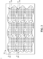
- Fig. 3 is a schematic view of the electronic apparatus 1 in accordance with some embodiments of the present disclosure.
- Fig. 4 is a schematic view of the display panel 20 in accordance with some embodiments of the present disclosure.
- the display panel 20 may be a polygonal or irregular shape.
- the polygon may be a triangle, a quadrangle, a pentagon, or a hexagon.
- the display panels 20 are irregular shapes and are connected to each other.
- the irregular electronic apparatus 1 may have regions as the embodiment of Fig. 2 (such as the first left region Z11, the second left region Z12, the first right region Z21, and the second right region Z22).
- the difference from Fig. 2 is that the boundaries T11, T12, T13, T14, and T15 in Fig. 4 are curved, and the shape of the curves is approximately similar to edges E11 and E12.
- the remaining features are the same as those in Fig. 2 , and are not described again herein.
- the length of the display panel 20a is the maximum distance d16 from edge E11 to edge E12 in the second direction D2.
- the width of the display panel 20a is the maximum distance d17 from edge E13 to edge E14 in the first direction D1.
- edge E11 and edge E12 may not be parallel to each other and may have different lengths.
- the shape of the boundaries T11, T12, T13 and T14 correspond to the shape of the edge E11 in the second direction D2, and the length of the boundaries T11, T12, T13 and T14 may be different from the edge E11.
- the length of the display panel 20b is the maximum distance d26 from edge E21 to edge E22 in the second direction D2.
- the width of the display panel 20a is the maximum distance d27 from edge E13 to edge E14 in the first direction D1.
- edge E21 and edge E22 may not be parallel to each other and may have different lengths.
- the shape of the boundaries T11, T12, T13 and T14 correspond to the shape of the edge E21 in the second direction D2, and the length of the boundaries T11, T12, T13 and T14 may be different from the edge E21.
- regions such as the first left region Z11 and the first right region Z21
- the display panels 20 are connected in the second direction D2.
- the display panels 20 are connected in the first direction D1 (not shown), and have applicable regions and features, though they are not described herein.
- Fig. 5 is a schematic view of the display panels 20 in accordance with some embodiments of the present disclosure.
- the pitches d3(first pitch) of each of the centers of two adjacent light-emitting elements 21 are the same.
- the pitch d4 (second pitch) of the centers of two adjacent light-emitting elements 21 for example, the adjacent light-emitting elements 21a and 21b of two adjacent display panels 20 (for example, the display panels 20a and 20b) is different from pitch d3 (first pitch) due to the deviation of the edge of the display panels 20. Therefore, the quality of the integrated image may be decreased.
- the cutting regions Z3 and Z4 of the display panels 20 can be cut so that the pitch d3 (first pitch) of each of the centers of the two adjacent light-emitting elements 21 can be equal.
- Fig. 6 is a schematic view of the display panel 20 in accordance with some embodiments of the present disclosure.
- the minimum distance (vertical distance) between the center of the light-emitting elements (first light-emitting elements) 21a of the display panel 20a and the edge E11 in the second direction D2 is shortened.
- the minimum distance (vertical distance) between the center of the light-emitting elements (first light-emitting elements) 21b of the display panel 20b and the edge E21 in the second direction D2 is shortened.
- the relative positions of the display panel 20a and the display panel 20b can be adjusted.
- the pitch d3 (first pitch) between the centers of two adjacent light-emitting elements 21a in the second direction may be substantially equal to the pitch d4 (second pitch) between the centers of the light-emitting elements 21a adjacent to the edge E11 and the light-emitting elements 21b adjacent to the edge E21 in the second direction, wherein the pitch d4 (second pitch) may be 70% to 130% the pitch d3 (first pitch).
- a ratio of the second pitch to the first pitch is in a range from 0.7 to 1.3.
- the pitch d3 (first pitch) between the centers of two adjacent light-emitting elements 21b in the second direction may be substantially equal to the pitch d4 (second pitch) between the centers of the light-emitting elements 21a adjacent to the edge E11 and the light-emitting elements 21b adjacent to the edge E21 in the second direction, wherein the pitch d4 (second pitch) may be 70% to 130% the pitch d3 (first pitch).
- a ratio of the second pitch to the first pitch is in a range from 0.7 to 1.3.
- the electronic device of the present disclosure can also have the same features in the first direction D1, and may not be described here.
- a low-reflection material M1 may be disposed between the edge E11 of the display panel 20a and the edge E21 of the display panel 20b.
- the reflectivity of the low-reflection material M1 may be in a range from 0% to 10%.
- the low-reflection material M1 may be black.
- the difference of the reflectivity between the surfaces of low-reflection material M1 and the display panels 20 (20a, 20b, 20c and 20d) may be in a range from 0% to 10%.
- the difference of the reflectivity between the low-reflection material M1 and the display panel 20 may be reduced by the low-reflection material M1, and thus the quality of the integrated image may be improved.
- the low-reflection material M1 may be disposed between the edge E14 of the display panel 20a and the edge of the display panel (third display panel) 20c.
- the low-reflection material M1 may be disposed between the edge of the display panel 20b and the edge of the display panel (third display panel) 20d.
- the low-reflection material M1 may be disposed between the edge of the display panel 20c and the edge of the display panel 20d.
- the reflection of light between two display panels 20 may be reduced by the low-reflection material M1, and thus the quality of the integrated image may be improved.
- the difference between low-reflection material M1 and display panel 20 for light reflectivity may be reduced by the low-reflection material M1, and thus the quality of the integrated image may be improved.
- the display panel 20 further includes a shading material M2 disposed between the light-emitting elements 21.
- the shading material M2 may around each light-emitting element 21.
- the shading material (first shading material) M2 may be disposed between the light-emitting elements 21a of the display panel 20a.
- the shading material (second shading material) M2 may be disposed between the light-emitting elements 21b of the display panel 20b.
- the shading material M2 may include polymerized siloxanes, polycarbonate) or other insulating material or flexible material.
- the reflectivity of the shading material M2 may be in a range from 0% to 10%.
- the reflectivity of the material or display panel can be obtained by measuring the positive viewing angle with a spectrophotometer.
- Fig. 7 is a schematic view of the display panel 20 in accordance with some embodiments of the present disclosure. There are nine display panels 20 shown in Fig. 7 .
- the electronic apparatus 1 further includes circuit boards 30, electrical connectors 41, electrical connectors 42, electrical connectors 43, and electrical connectors 44.
- the circuit boards 30 are disposed on the rear surfaces of the display panels 20.
- the electrical connector 41, the electrical connector 42, the electrical connector 43, and the electrical connector 44 are disposed on the circuit board 30.
- the electrical connectors 41 and the electrical connectors 42 are located at two opposite sides of the circuit boards 30.
- the electrical connectors 43 and the electrical connectors 44 are located at two opposite sides of the circuit boards 30.
- electrical connectors 41 and electrical connectors 42 are arranged in the first direction D1.
- electrical connectors 43 and electrical connectors 44 are arranged in the second direction D2.
- electrical connector (first electrical connector) 42 of the display panel 20a may be connected to electrical connector (second electrical connector) 41 of the display panel 20c via a connection cable W1.
- Electrical connector 42 of the display panel 20c may be connected to electrical connector 41 of the display panel 20e via a connection cable W1.
- the electrical connector 42 of the display panel 20e may be connected to a signal source (not shown).
- the image signal generated by the signal source can be transmitted to display panel 20e, display panel 20c, and display panel 20a via the connection cable W1. Accordingly, use of the connection module W1, electrical connector 41 and electrical connector 42 may reduce the complexity of connecting the display panel 20 to the signal source.
- electrical connector 44 of the display panel 20a may be connected to electrical connector 43 of the display panel 20b via a connection cable W2.
- Electrical connector 44 of the display panel 20b may be connected to electrical connector 43 of the display panel 20f via a connection cable W2.
- the display panel 20f the electrical connector 44 may be connected to a power supply (not shown).
- the power generated by the power source can be transmitted to display panel 20f, display panel 20b, and display panel 20a via the connection cable W2. Accordingly, in the embodiment, the process of connecting the display panel 20 to the power supply may be simplified by using the connection cable W2, electrical connector 43, and electrical connector 44.
- the electronic apparatus of the present disclosure may improve the quality of an integrated image by connecting display panels with only small differences in brightness and chromaticity.
- the pitch of each two adjacent light-emitting elements may be made equal by cutting the edge of the display panels.
- the reflection of light on the display panel may be reduced by disposing the low-reflection material on the edge of the display panel and reducing the shading material around the light-emitting elements.
- the gap between display panels may be made less noticeable by disposing materials having approximately the same reflectivity as the display panels on the edge of the display panel.
- a connection cable may be used to connect multiple display panels in series to reduce the complexity of the assembly of the electronic apparatus.
Landscapes
- Engineering & Computer Science (AREA)
- Physics & Mathematics (AREA)
- Computer Hardware Design (AREA)
- General Physics & Mathematics (AREA)
- Theoretical Computer Science (AREA)
- Chemical & Material Sciences (AREA)
- Crystallography & Structural Chemistry (AREA)
- Electroluminescent Light Sources (AREA)
- Devices For Indicating Variable Information By Combining Individual Elements (AREA)
Applications Claiming Priority (2)
| Application Number | Priority Date | Filing Date | Title |
|---|---|---|---|
| US201862659787P | 2018-04-19 | 2018-04-19 | |
| CN201811124400.8A CN110400537B (zh) | 2018-04-19 | 2018-09-26 | 电子设备 |
Publications (1)
| Publication Number | Publication Date |
|---|---|
| EP3557564A1 true EP3557564A1 (fr) | 2019-10-23 |
Family
ID=66323654
Family Applications (1)
| Application Number | Title | Priority Date | Filing Date |
|---|---|---|---|
| EP19167437.3A Withdrawn EP3557564A1 (fr) | 2018-04-19 | 2019-04-04 | Panneaux d'affichage électroniques |
Country Status (2)
| Country | Link |
|---|---|
| US (1) | US11164509B2 (fr) |
| EP (1) | EP3557564A1 (fr) |
Families Citing this family (2)
| Publication number | Priority date | Publication date | Assignee | Title |
|---|---|---|---|---|
| CN110400537B (zh) * | 2018-04-19 | 2021-03-30 | 群创光电股份有限公司 | 电子设备 |
| CN117496836B (zh) * | 2023-02-10 | 2025-09-09 | 武汉华星光电技术有限公司 | 背光面板 |
Citations (3)
| Publication number | Priority date | Publication date | Assignee | Title |
|---|---|---|---|---|
| US20100259566A1 (en) * | 2007-11-22 | 2010-10-14 | Sharp Kabushiki Kaisha | Display device |
| US20150116343A1 (en) * | 2013-10-28 | 2015-04-30 | Kabushiki Kaisha Toshiba | Electronic device and image reproducing characteristics determination method |
| US20180040271A1 (en) * | 2016-08-03 | 2018-02-08 | Samsung Electronics Co., Ltd. | Display apparatus and control method thereof |
Family Cites Families (8)
| Publication number | Priority date | Publication date | Assignee | Title |
|---|---|---|---|---|
| US6822389B2 (en) | 2001-10-11 | 2004-11-23 | Intel Corporation | Array display including resilient material in the seam |
| TWM361204U (en) * | 2008-11-18 | 2009-07-11 | Wistron Corp | Electronic device |
| CN105845036A (zh) * | 2015-01-14 | 2016-08-10 | 丁炜慷 | 一种拼接后“像素全覆盖”的“全无缝”显示幕墙系统 |
| TWI562107B (en) | 2015-04-23 | 2016-12-11 | Internat Liquid Crystal Display Co Ltd | Display |
| KR102542853B1 (ko) * | 2016-04-25 | 2023-06-14 | 삼성전자주식회사 | Led 디스플레이 모듈, 디스플레이 장치 및 제어 방법 |
| KR102534149B1 (ko) | 2016-05-24 | 2023-05-19 | 삼성디스플레이 주식회사 | 표시 장치, 그것의 제조 방법, 및 멀티 표시 장치 |
| JP6840948B2 (ja) * | 2016-07-25 | 2021-03-10 | 船井電機株式会社 | 液晶表示装置 |
| KR102415838B1 (ko) * | 2017-11-28 | 2022-06-30 | 엘지디스플레이 주식회사 | 다중 패널 표시장치 |
-
2019
- 2019-03-21 US US16/360,481 patent/US11164509B2/en active Active
- 2019-04-04 EP EP19167437.3A patent/EP3557564A1/fr not_active Withdrawn
Patent Citations (3)
| Publication number | Priority date | Publication date | Assignee | Title |
|---|---|---|---|---|
| US20100259566A1 (en) * | 2007-11-22 | 2010-10-14 | Sharp Kabushiki Kaisha | Display device |
| US20150116343A1 (en) * | 2013-10-28 | 2015-04-30 | Kabushiki Kaisha Toshiba | Electronic device and image reproducing characteristics determination method |
| US20180040271A1 (en) * | 2016-08-03 | 2018-02-08 | Samsung Electronics Co., Ltd. | Display apparatus and control method thereof |
Also Published As
| Publication number | Publication date |
|---|---|
| US20190325814A1 (en) | 2019-10-24 |
| US11164509B2 (en) | 2021-11-02 |
Similar Documents
| Publication | Publication Date | Title |
|---|---|---|
| US20250014511A1 (en) | Electronic apparatus | |
| US8736802B2 (en) | Liquid crystal display (LCD) | |
| US9377174B2 (en) | Display device | |
| US8089440B2 (en) | Liquid crystal flat panel display with an integral heater of predeterminable capacity | |
| US11474401B2 (en) | Display panel and fabrication method thereof, and display apparatus | |
| US20160054614A1 (en) | Display device | |
| US20160253022A1 (en) | In-cell touch panel and display device | |
| US20190228722A1 (en) | Display apparatus including a luminance compensating part and method of driving the same | |
| CN115268153B (zh) | 一种阵列基板及显示装置 | |
| US20250098319A1 (en) | Display panel and display apparatus | |
| EP3557564A1 (fr) | Panneaux d'affichage électroniques | |
| US10948792B2 (en) | Liquid crystal display device | |
| US11360352B2 (en) | Display panel, display apparatus and display device | |
| KR101787745B1 (ko) | 액정표시장치 | |
| US20240248360A1 (en) | Display panel and display device | |
| US20140176889A1 (en) | Liquid Crystal Display Device | |
| KR20190098294A (ko) | 표시 장치 | |
| CN102621753B (zh) | 像素结构以及显示面板 | |
| US11513406B2 (en) | Display panel, display device and repairing method of display panel | |
| US10247989B2 (en) | TFT array substrate, liquid crystal display panel and liquid crystal display device | |
| CN106910446A (zh) | 一种显示面板 | |
| US12055832B1 (en) | Array substrate comprising a keel electrode configured to load a colored-film-substrate common voltage and display panel | |
| US12020656B2 (en) | Display device | |
| CN116819835B (zh) | 一种显示模组及显示装置 | |
| US20250130467A1 (en) | Liquid crystal display device |
Legal Events
| Date | Code | Title | Description |
|---|---|---|---|
| PUAI | Public reference made under article 153(3) epc to a published international application that has entered the european phase |
Free format text: ORIGINAL CODE: 0009012 |
|
| STAA | Information on the status of an ep patent application or granted ep patent |
Free format text: STATUS: THE APPLICATION HAS BEEN PUBLISHED |
|
| AK | Designated contracting states |
Kind code of ref document: A1 Designated state(s): AL AT BE BG CH CY CZ DE DK EE ES FI FR GB GR HR HU IE IS IT LI LT LU LV MC MK MT NL NO PL PT RO RS SE SI SK SM TR |
|
| AX | Request for extension of the european patent |
Extension state: BA ME |
|
| STAA | Information on the status of an ep patent application or granted ep patent |
Free format text: STATUS: THE APPLICATION IS DEEMED TO BE WITHDRAWN |
|
| 18D | Application deemed to be withdrawn |
Effective date: 20200603 |