EP3555681B1 - Optical switch network - Google Patents
Optical switch network Download PDFInfo
- Publication number
- EP3555681B1 EP3555681B1 EP17829428.6A EP17829428A EP3555681B1 EP 3555681 B1 EP3555681 B1 EP 3555681B1 EP 17829428 A EP17829428 A EP 17829428A EP 3555681 B1 EP3555681 B1 EP 3555681B1
- Authority
- EP
- European Patent Office
- Prior art keywords
- optical
- optical switch
- binary
- waveguide
- switches
- Prior art date
- Legal status (The legal status is an assumption and is not a legal conclusion. Google has not performed a legal analysis and makes no representation as to the accuracy of the status listed.)
- Active
Links
- 230000003287 optical effect Effects 0.000 title claims description 501
- 230000008878 coupling Effects 0.000 claims description 25
- 238000010168 coupling process Methods 0.000 claims description 25
- 238000005859 coupling reaction Methods 0.000 claims description 25
- 239000011159 matrix material Substances 0.000 claims description 18
- 239000013307 optical fiber Substances 0.000 claims description 13
- 230000004044 response Effects 0.000 claims description 5
- 238000003491 array Methods 0.000 description 20
- 238000010586 diagram Methods 0.000 description 15
- 239000000463 material Substances 0.000 description 13
- 239000000758 substrate Substances 0.000 description 11
- 238000004891 communication Methods 0.000 description 9
- 239000003086 colorant Substances 0.000 description 8
- 239000007787 solid Substances 0.000 description 8
- XUIMIQQOPSSXEZ-UHFFFAOYSA-N Silicon Chemical compound [Si] XUIMIQQOPSSXEZ-UHFFFAOYSA-N 0.000 description 7
- 238000000034 method Methods 0.000 description 7
- 229910052710 silicon Inorganic materials 0.000 description 7
- 239000010703 silicon Substances 0.000 description 7
- 235000012431 wafers Nutrition 0.000 description 6
- 238000013459 approach Methods 0.000 description 4
- 238000004519 manufacturing process Methods 0.000 description 4
- 239000004065 semiconductor Substances 0.000 description 4
- 229910052581 Si3N4 Inorganic materials 0.000 description 3
- 238000005286 illumination Methods 0.000 description 3
- 230000000737 periodic effect Effects 0.000 description 3
- 230000008569 process Effects 0.000 description 3
- HQVNEWCFYHHQES-UHFFFAOYSA-N silicon nitride Chemical compound N12[Si]34N5[Si]62N3[Si]51N64 HQVNEWCFYHHQES-UHFFFAOYSA-N 0.000 description 3
- IJGRMHOSHXDMSA-UHFFFAOYSA-N Atomic nitrogen Chemical compound N#N IJGRMHOSHXDMSA-UHFFFAOYSA-N 0.000 description 2
- VYPSYNLAJGMNEJ-UHFFFAOYSA-N Silicium dioxide Chemical compound O=[Si]=O VYPSYNLAJGMNEJ-UHFFFAOYSA-N 0.000 description 2
- 230000004075 alteration Effects 0.000 description 2
- 230000006870 function Effects 0.000 description 2
- 239000011521 glass Substances 0.000 description 2
- 238000012986 modification Methods 0.000 description 2
- 230000004048 modification Effects 0.000 description 2
- 229920000642 polymer Polymers 0.000 description 2
- 238000012545 processing Methods 0.000 description 2
- 230000005855 radiation Effects 0.000 description 2
- 238000003860 storage Methods 0.000 description 2
- 239000013589 supplement Substances 0.000 description 2
- 230000003213 activating effect Effects 0.000 description 1
- 239000011149 active material Substances 0.000 description 1
- 230000008901 benefit Effects 0.000 description 1
- 230000005540 biological transmission Effects 0.000 description 1
- 239000013590 bulk material Substances 0.000 description 1
- 230000008859 change Effects 0.000 description 1
- 238000004590 computer program Methods 0.000 description 1
- 238000007796 conventional method Methods 0.000 description 1
- 238000009826 distribution Methods 0.000 description 1
- 230000000694 effects Effects 0.000 description 1
- 230000005670 electromagnetic radiation Effects 0.000 description 1
- 239000007789 gas Substances 0.000 description 1
- 229910052757 nitrogen Inorganic materials 0.000 description 1
- 230000005693 optoelectronics Effects 0.000 description 1
- 238000002161 passivation Methods 0.000 description 1
- 230000010363 phase shift Effects 0.000 description 1
- 239000000377 silicon dioxide Substances 0.000 description 1
- 230000000153 supplemental effect Effects 0.000 description 1
- 239000011800 void material Substances 0.000 description 1
Images


Classifications
-
- G—PHYSICS
- G02—OPTICS
- G02B—OPTICAL ELEMENTS, SYSTEMS OR APPARATUS
- G02B6/00—Light guides; Structural details of arrangements comprising light guides and other optical elements, e.g. couplings
- G02B6/24—Coupling light guides
- G02B6/26—Optical coupling means
- G02B6/35—Optical coupling means having switching means
- G02B6/354—Switching arrangements, i.e. number of input/output ports and interconnection types
- G02B6/3544—2D constellations, i.e. with switching elements and switched beams located in a plane
- G02B6/3548—1xN switch, i.e. one input and a selectable single output of N possible outputs
-
- B—PERFORMING OPERATIONS; TRANSPORTING
- B81—MICROSTRUCTURAL TECHNOLOGY
- B81B—MICROSTRUCTURAL DEVICES OR SYSTEMS, e.g. MICROMECHANICAL DEVICES
- B81B3/00—Devices comprising flexible or deformable elements, e.g. comprising elastic tongues or membranes
- B81B3/0064—Constitution or structural means for improving or controlling the physical properties of a device
- B81B3/0083—Optical properties
-
- G—PHYSICS
- G01—MEASURING; TESTING
- G01S—RADIO DIRECTION-FINDING; RADIO NAVIGATION; DETERMINING DISTANCE OR VELOCITY BY USE OF RADIO WAVES; LOCATING OR PRESENCE-DETECTING BY USE OF THE REFLECTION OR RERADIATION OF RADIO WAVES; ANALOGOUS ARRANGEMENTS USING OTHER WAVES
- G01S17/00—Systems using the reflection or reradiation of electromagnetic waves other than radio waves, e.g. lidar systems
- G01S17/88—Lidar systems specially adapted for specific applications
- G01S17/89—Lidar systems specially adapted for specific applications for mapping or imaging
-
- G—PHYSICS
- G01—MEASURING; TESTING
- G01S—RADIO DIRECTION-FINDING; RADIO NAVIGATION; DETERMINING DISTANCE OR VELOCITY BY USE OF RADIO WAVES; LOCATING OR PRESENCE-DETECTING BY USE OF THE REFLECTION OR RERADIATION OF RADIO WAVES; ANALOGOUS ARRANGEMENTS USING OTHER WAVES
- G01S7/00—Details of systems according to groups G01S13/00, G01S15/00, G01S17/00
- G01S7/48—Details of systems according to groups G01S13/00, G01S15/00, G01S17/00 of systems according to group G01S17/00
- G01S7/481—Constructional features, e.g. arrangements of optical elements
- G01S7/4814—Constructional features, e.g. arrangements of optical elements of transmitters alone
-
- G—PHYSICS
- G01—MEASURING; TESTING
- G01S—RADIO DIRECTION-FINDING; RADIO NAVIGATION; DETERMINING DISTANCE OR VELOCITY BY USE OF RADIO WAVES; LOCATING OR PRESENCE-DETECTING BY USE OF THE REFLECTION OR RERADIATION OF RADIO WAVES; ANALOGOUS ARRANGEMENTS USING OTHER WAVES
- G01S7/00—Details of systems according to groups G01S13/00, G01S15/00, G01S17/00
- G01S7/48—Details of systems according to groups G01S13/00, G01S15/00, G01S17/00 of systems according to group G01S17/00
- G01S7/481—Constructional features, e.g. arrangements of optical elements
- G01S7/4816—Constructional features, e.g. arrangements of optical elements of receivers alone
-
- G—PHYSICS
- G01—MEASURING; TESTING
- G01S—RADIO DIRECTION-FINDING; RADIO NAVIGATION; DETERMINING DISTANCE OR VELOCITY BY USE OF RADIO WAVES; LOCATING OR PRESENCE-DETECTING BY USE OF THE REFLECTION OR RERADIATION OF RADIO WAVES; ANALOGOUS ARRANGEMENTS USING OTHER WAVES
- G01S7/00—Details of systems according to groups G01S13/00, G01S15/00, G01S17/00
- G01S7/48—Details of systems according to groups G01S13/00, G01S15/00, G01S17/00 of systems according to group G01S17/00
- G01S7/481—Constructional features, e.g. arrangements of optical elements
- G01S7/4817—Constructional features, e.g. arrangements of optical elements relating to scanning
-
- G—PHYSICS
- G02—OPTICS
- G02B—OPTICAL ELEMENTS, SYSTEMS OR APPARATUS
- G02B26/00—Optical devices or arrangements for the control of light using movable or deformable optical elements
- G02B26/007—Optical devices or arrangements for the control of light using movable or deformable optical elements the movable or deformable optical element controlling the colour, i.e. a spectral characteristic, of the light
-
- G—PHYSICS
- G02—OPTICS
- G02B—OPTICAL ELEMENTS, SYSTEMS OR APPARATUS
- G02B6/00—Light guides; Structural details of arrangements comprising light guides and other optical elements, e.g. couplings
- G02B6/24—Coupling light guides
- G02B6/26—Optical coupling means
- G02B6/35—Optical coupling means having switching means
- G02B6/351—Optical coupling means having switching means involving stationary waveguides with moving interposed optical elements
- G02B6/3524—Optical coupling means having switching means involving stationary waveguides with moving interposed optical elements the optical element being refractive
- G02B6/3526—Optical coupling means having switching means involving stationary waveguides with moving interposed optical elements the optical element being refractive the optical element being a lens
-
- G—PHYSICS
- G02—OPTICS
- G02B—OPTICAL ELEMENTS, SYSTEMS OR APPARATUS
- G02B6/00—Light guides; Structural details of arrangements comprising light guides and other optical elements, e.g. couplings
- G02B6/24—Coupling light guides
- G02B6/26—Optical coupling means
- G02B6/35—Optical coupling means having switching means
- G02B6/351—Optical coupling means having switching means involving stationary waveguides with moving interposed optical elements
- G02B6/3534—Optical coupling means having switching means involving stationary waveguides with moving interposed optical elements the optical element being diffractive, i.e. a grating
-
- G—PHYSICS
- G02—OPTICS
- G02B—OPTICAL ELEMENTS, SYSTEMS OR APPARATUS
- G02B6/00—Light guides; Structural details of arrangements comprising light guides and other optical elements, e.g. couplings
- G02B6/24—Coupling light guides
- G02B6/26—Optical coupling means
- G02B6/35—Optical coupling means having switching means
- G02B6/354—Switching arrangements, i.e. number of input/output ports and interconnection types
- G02B6/3544—2D constellations, i.e. with switching elements and switched beams located in a plane
- G02B6/3548—1xN switch, i.e. one input and a selectable single output of N possible outputs
- G02B6/355—1x2 switch, i.e. one input and a selectable single output of two possible outputs
-
- H—ELECTRICITY
- H04—ELECTRIC COMMUNICATION TECHNIQUE
- H04J—MULTIPLEX COMMUNICATION
- H04J14/00—Optical multiplex systems
- H04J14/02—Wavelength-division multiplex systems
- H04J14/0201—Add-and-drop multiplexing
- H04J14/0215—Architecture aspects
- H04J14/022—For interconnection of WDM optical networks
-
- H—ELECTRICITY
- H04—ELECTRIC COMMUNICATION TECHNIQUE
- H04Q—SELECTING
- H04Q11/00—Selecting arrangements for multiplex systems
- H04Q11/0001—Selecting arrangements for multiplex systems using optical switching
- H04Q11/0003—Details
-
- H—ELECTRICITY
- H04—ELECTRIC COMMUNICATION TECHNIQUE
- H04Q—SELECTING
- H04Q11/00—Selecting arrangements for multiplex systems
- H04Q11/0001—Selecting arrangements for multiplex systems using optical switching
- H04Q11/0005—Switch and router aspects
-
- B—PERFORMING OPERATIONS; TRANSPORTING
- B81—MICROSTRUCTURAL TECHNOLOGY
- B81B—MICROSTRUCTURAL DEVICES OR SYSTEMS, e.g. MICROMECHANICAL DEVICES
- B81B2201/00—Specific applications of microelectromechanical systems
- B81B2201/04—Optical MEMS
- B81B2201/045—Optical switches
-
- G—PHYSICS
- G02—OPTICS
- G02B—OPTICAL ELEMENTS, SYSTEMS OR APPARATUS
- G02B6/00—Light guides; Structural details of arrangements comprising light guides and other optical elements, e.g. couplings
- G02B6/10—Light guides; Structural details of arrangements comprising light guides and other optical elements, e.g. couplings of the optical waveguide type
- G02B6/12—Light guides; Structural details of arrangements comprising light guides and other optical elements, e.g. couplings of the optical waveguide type of the integrated circuit kind
- G02B2006/12133—Functions
- G02B2006/12145—Switch
Definitions
- the present invention relates to optical switches and, more particularly, to optical switch networks used to control directions in which optical signals are transmitted or received, such as in light direction and ranging (LiDAR) and laser communication systems.
- LiDAR light direction and ranging
- optical systems need to emit or receive a (humanly visible or invisible) collimated optical beam in a direction that can be controlled with high precision.
- such optical beams are used in light direction and ranging (LiDAR) systems, and often these beams need to be steered or swept to locate or track a target.
- laser communications systems sometimes need to steer an optical beam, such as to initially establish a line-of-sight communications channel between two terminals or if one or both of the terminals moves.
- LiDAR light direction and ranging
- laser communications systems sometimes need to steer an optical beam, such as to initially establish a line-of-sight communications channel between two terminals or if one or both of the terminals moves.
- From Document US2002/048423A1 an optical switch network for in-plan distribution of light and switching between channels by grating switches in bulk material is known.
- WO2008/045126 A2 an integrated LIDAR system utilizing opto-electronic components is known.
- Prior art LiDAR and laser communications terminals use telescopes and either point the entire telescope using a gimbal or place a moveable steering mirror in front of the telescope and use the mirror to redirect the beam, as exemplified by U.S. Pat. Publ. No. 2007/0229994 .
- this approach requires large and bulky moving systems, with attendant disadvantages in terms of size, mass, power and reliability.
- phased arrays In which a large number of antennas are arrayed closely together and operated coherently, i.e., the phases of the individual emitters are carefully controlled to make the entire array operate in unison. Signals in the near field constructively and destructively interfere to create nulls and reinforced signals in desired directions.
- phased arrays require large numbers of emitters and associated optical phase adjusters.
- a nominal optical phased array has emitters disposed at half-wavelength spacings, i.e. apx. 0.5 ⁇ m.
- the required total aperture size might be on the order of 5 cm.
- phase shifters requires apx. 1 mW of power to operate.
- the total power consumption of such an array might approach 10 5 W, an impractically large amount of power.
- limitations on the densities at which binary optical switches may be fabricated limit spatial resolution of the transmit/receive terminal, i.e., density of possible transmit or receive beam positions.
- An embodiment of the present invention provides an optical switch network according to claim 1.
- the optical switch network include a common input/output port, a waveguide having a length and being optically coupled to the common input/output port, and a plurality of binary optical switches disposed on a planar surface.
- the plurality of binary optical switches is disposed along the length of the waveguide.
- Each binary optical switch of the plurality of binary optical switches includes a translatable optical grating and a MEMS structure.
- the translatable optical grating is configured to translate between at least two positions.
- T first position of the at least two positions is sufficiently close to the waveguide to optically couple between the waveguide and free space beyond the planar surface with a coupling efficiency of at least about 25%
- a second position of the at least two positions is sufficiently far from the waveguide to optically couple between the waveguide and the free space with a coupling efficiency of at most about 5%.
- the MEMS structure is configured to selectively translate the translatable optical grating to the first position and to the second position.
- the N other ports may be arranged in a rectangular array.
- the N other ports may be disposed on a planar surface.
- the optical switch network may include or be fabricated on a photonic chip.
- Each port of the N other ports may include an optical coupler.
- the optical switch network may also include a row-and-column addressing matrix having a plurality of rows and a plurality of columns.
- Each first binary optical switch of the plurality of first binary optical switches and each second binary optical switch of the plurality of second binary optical switches may be coupled to a row of the plurality of rows, coupled to a column of the plurality of columns, and configured to actuate in response to signals being present on both the row of the plurality of rows and the column of the plurality of columns.
- the optical send/receive terminal includes a lens having a field of view.
- the optical send/receive terminal also includes an optical switch network.
- the optical switch network includes a common input/output port, a plurality of N other ports optically coupled to the lens, such that each port of the plurality of N other ports is optically coupled to a unique portion of the lens field of view.
- the optical switch network also includes a first waveguide optically coupled to the common input/output port and a plurality of first binary optical switches optically coupled to the first waveguide.
- the plurality of first binary optical switches is disposed along the length of the first waveguide.
- the optical switch network also includes a plurality of second waveguides.
- Each second waveguide of the plurality of second waveguides is optically coupled to the first waveguide via a respective first binary optical switch of the plurality of first binary optical switches.
- a respective plurality of second binary optical switches is optically coupled to the second waveguide of the plurality of second waveguides.
- Each plurality of second binary optical switches is disposed along the length of the respective second waveguide.
- Each second binary optical switch of the plurality of second binary optical switches is optically coupled between the respective second waveguide of the plurality of second waveguides and a respective port of the plurality of N other ports.
- Each second binary optical switch of the plurality of second binary optical switches includes a translatable optical grating and a MEMS structure.
- the translatable optical grating is configured to translate between at least two positions, a first position of the at least two positions being sufficiently close to the respective second waveguide to optically couple with the second waveguide with a coupling efficiency of at least about 25%, and a second position of the at least two positions being sufficiently far from the respective second waveguide to optically couple with the second waveguide with a coupling efficiency of at most about 5%.
- the MEMS structure is configured to selectively translate the translatable optical grating to the first position and to the second position.
- An optical transmitter and/or an optical receiver is optically coupled to the common input/output port of the optical switch network.
- the optical send/receive terminal may also include a plurality of optical fibers optically coupling the N other ports to the lens.
- the optical switch network may define a surface and each second binary optical switch of the plurality of second binary optical switches may be configured, when the second binary optical switch is in the first position, to optically couple between the respective second waveguide and free space beyond the surface of the optical switch network.
- Each translatable optical grating may include a respective MEMS structure.
- Each first binary optical switch of the plurality of first binary optical switches may include a respective MEMS structure.
- the optical send/receive terminal may also include a row-and-column addressing matrix having a plurality of rows and a plurality of columns.
- Each first binary optical switch of the plurality of first binary optical switches and each second binary optical switch of the plurality of second binary optical switches may be coupled to a row of the plurality of rows, coupled to a column of the plurality of columns, and configured to actuate in response to signals being present on both the row of the plurality of rows and the column of the plurality of columns.
- the optical terminal includes a lens having a field of view and a planar optical switch that includes a plurality of optical switch arrays.
- Each optical switch array of the plurality of optical switch arrays may include a common port and a plurality of N other ports optically coupled to the lens.
- Each port of the plurality of N other ports is optically coupled to a unique portion of the lens field of view.
- a planar Nx1 optical switch network optically is coupled between the common port and the plurality of N other ports.
- An optical receiver optically coupled to the common port.
- Each optical switch array of the plurality of optical switch arrays may also include an optical transmitter optically coupled to the common port.
- the optical terminal may also include an optical transmitter optically coupled to the common port of at least one optical switch array of the plurality of optical switch arrays.
- the optical terminal may also include an optical transmitter optically coupled to the common ports of the plurality of optical switch arrays.
- the planar optical switch may define a plane.
- the planar Nx1 optical switch network may include a waveguide having a length and being optically coupled to the common port of the optical switch array.
- a plurality of binary optical switches may be disposed on the plane of the planar optical switch.
- the plurality of binary optical switches may be disposed along the length of the waveguide.
- Each binary optical switch of the plurality of binary optical switches may include a translatable optical grating and a MEMS structure.
- the translatable optical grating may be configured to translate between at least two positions, a first position of the at least two positions being sufficiently close to the waveguide to optically couple between the waveguide and free space beyond the plane of the planar optical switch with a coupling efficiency of at least about 25%, and a second position of the at least two positions being sufficiently far from the waveguide to optically couple between the waveguide and the free space with a coupling efficiency of at most about 5%.
- the MEMS structure may be configured to selectively translate the translatable optical grating to the first position and to the second position.
- a planar optical switch defines a planar surface and includes a plurality of optical switch arrays.
- Each optical switch array of the plurality of optical switch arrays includes a common port, a waveguide having a length and being optically coupled to the common port.
- a plurality of binary optical switches is disposed on the planar surface. The plurality of binary optical switches is disposed along the length of the waveguide.
- Each binary optical switch of the plurality of binary optical switches includes a translatable optical grating and a MEMS structure.
- the translatable optical grating is configured to translate between at least two positions, a first position of the at least two positions being sufficiently close to the waveguide to optically couple between the waveguide and free space beyond the planar surface with a coupling efficiency of at least about 25%, and a second position of the at least two positions being sufficiently far from the waveguide to optically couple between the waveguide and the free space with a coupling efficiency of at most about 5%.
- the MEMS structure is configured to selectively translate the translatable optical grating to the first position and to the second position.
- Yet another example not forming part of the present invention provides an optical system that includes a lenticular lens having a field of view and a plurality of ports.
- the plurality of ports is disposed such that, for each port of the plurality of ports, a unique portion of the field of view is visible, through the lenticular lens, by the port.
- An optical switch network has an input port and is configured to optically couple the input port to a selected port of the plurality of ports in response to a control signal.
- the optical switch network may define a planar surface.
- the optical switch network may include a waveguide having a length and being optically coupled to the input port.
- a plurality of binary optical switches may be disposed on a planar surface.
- the plurality of binary optical switch may be disposed along the length of the waveguide.
- Each binary optical switch of the plurality of binary optical switches may include a translatable optical grating and a MEMS structure.
- the translatable optical grating may be configured to translate between at least two positions, a first position of the at least two positions being sufficiently close to the waveguide to optically couple between the waveguide and free space beyond the planar surface with a coupling efficiency of at least about 25%, and a second position of the at least two positions being sufficiently far from the waveguide to optically couple between the waveguide and the free space with a coupling efficiency of at most about 5%.
- the MEMS structure may be configured to selectively translate the translatable optical grating to the first position and to the second position.
- the optical switch network may include a wavelength filter and a wavelength tunable light source.
- An example not forming part of the present invention provides a radiation projector that includes a lenticular lens.
- An input is configured to receive a time-varying illumination pattern.
- a nonophotonic array has a plurality of outputs.
- a filter is configured to direct the time-varying illumination pattern to a particular output of the nanophotonic array, so that the time-varying illumination from the output is directed to the lenticular lens.
- a steerable optical transmit and receive terminal and an associated MEMS-based optical switch network.
- Such a terminal does not require a phased array of emitters/collectors, nor the attendant large number of phase shifters.
- the optical switch network employs MEMS-based binary optical switches to steer the optical beam.
- the MEMS-based binary optical switches are significantly smaller than in the prior art, such as in H-tree based optical switch networks. Consequently, the MEMS-based binary optical switches may be fabricated or packed at a higher density than in the prior art, providing higher spatial resolution of the transmit/receive terminal, i.e., density of possible transmit/receive beam positions.
- a relatively small subset of the MEMS-based binary optical switches needs to be operated, therefore powered, at any given time. Therefore, the terminal overcomes the mechanical, switch density, emitter density and high power problems associated with the prior art.
- Fig. 1 is a schematic illustration of an all-solid state optical transmit/receive terminal 100.
- a lens 102 is optically coupled to an optical switch network 104 (also referred to herein as an "optical waveguide network” or an “optical switch”), such that incoming light rays, represented by light rays 106, are focused on a surface 107 of the optical switch network 104.
- optical signals emitted at the surface 107 of the optical switch network 104 are optically coupled to the lens and, thereby, projected into space as light rays 106.
- the light may be humanly visible or invisible, such as infrared (IR), light.
- the surface 107 may be a planar surface or a non-planar surface.
- the lens 102 is preferably a wide field-of-view lens.
- the lens 102 may, for example, be a gradient index (GRIN) lens, fisheye lens or monocentric lens.
- a suitable monocentric lens is available from Distant Focus Corporation, PO Box 7857, Champaign, IL 61826-7857.
- the lens 102 and the optical switch network 104 may be optically coupled by air or a vacuum 108.
- a bundle of optical fibers 108 may be used to optically couple the lens 102 to the optical switch network 104.
- each optical fiber of the bundle of optical fibers 108 may terminate on the surface of the lens 102, and the other end of the optical fiber may terminate on the surface 107 of the optical switch network 104.
- the ends of the optical fibers 108 that terminate on the surface of the lens 102 may have polished ends, forming curved surfaces that match curvature of the lens 102.
- Fig. 2 is a schematic diagram illustrating a plurality of N ports 200, represented by ports 202, 204, 206, 208 and 210, on the surface 107 of the optical switch network 104 of Fig. 1 .
- the plurality of ports 200 is shown as being arranged in a rectangular array. However, the ports 200 may be arranged in any suitable arrangement. If optical fibers 108 ( Fig. 1 ) are used to couple the lens 102 to the optical switch network 104, one or more optical fibers 108 may terminate at each port 202-210.
- the optical fibers 108 should be arranged so the image projected by the lens 102 is mapped to corresponding locations within the plurality of ports 200. Thus, each port 202-210 corresponds to a unique portion of the field of view of the lens 102.
- the optical switch network 104 also has a single common input/output port 110.
- the optical switch network 104 is configured to selectively optically couple one or more of the N ports 202-210 ( Fig. 2 ) on the surface 107 to the common input/output port 110.
- the optical switch network 104 acts as an Nxl switch. That is, one of the N ports 202-210 is coupled to the common input/output port 110.
- the optical switch network 104 acts as a plurality of Nxl switches. That is, a plurality of the N ports 202-210 are simultaneously coupled to the common input/output port 110.
- the terminal 100 also includes a suitable optical receiver 112, such as a photo diode, and/or a suitable transmitter 114, such as a laser.
- a LiDAR system or a two-way communication system includes both the transmitter 114 and the receiver 112.
- a one-way communication system need to include only the transmitter 114 or the receiver 112, and a star tracker needs to include only the receiver 112.
- the receiver 112 and/or transmitter 114 are optically coupled to the common input/output port 110 by suitable optical couplings, represented by optical coupling 116, such as optical fibers, mirrors and/or splitters/combiners.
- an optical signal from the transmitter 114 may be routed via the optical coupling 116 to the optical switch network 104 and there switched to a selected one or more of the N ports 202-210.
- the optical signal is conveyed to the lens 102, such as via the optical fiber(s) 108 terminated at the selected port(s) 202-210, and then by the lens 102 into space.
- a direction in space, in which the optical signal is projected by the lens 102 depends on which port(s) 202-210 is(are) selected.
- an optical signal received by the lens 102 such as a return signal in a LiDAR system, is routed by the optical switch network 104 to the receiver 112.
- a direction in space, from which the optical signal is received by the lens 102 depends on which port 202-210 is selected.
- Fig. 3 is a schematic diagram illustrating the optical switch network 104, according to an embodiment of the present invention.
- the right side of Fig. 3 shows an "H-tree" arrangement of optical waveguides (a branched optical waveguide network), rooted at the common input/output port 110.
- the left side of Fig. 3 shows a portion of the right side enlarged. Ports 202-210 are shown in Fig. 3 .
- a binary optical switch is disposed at each junction of two optical waveguides of the H-tree, as exemplified by binary optical switches 300, 302, 304, 306, 308 and 310.
- a binary optical switch routes an optical signal along either of two optical paths.
- the binary optical switches 300-308 determine a route for an optical signal traveling through the H-tree.
- a binary optical switch routes an optical signal along at most one of the two optical paths. For example, if an optical signal in introduced into the common input/output port 110, the binary optical switches 300-308 route the optical signal to one of the N ports 202-210. In the example depicted in Fig. 3 , the optical signal is routed to port 202.
- each binary optical switch is implemented with a Mach-Zender interferometer.
- An example of such a binary optical switch 400 is shown schematically in Fig. 4 .
- Light at input 402 is split between two paths 404 and 406.
- a phase shifter 408 and/or 410 is selectively enabled on one or both of the paths 404 and 406, and then the light is recombined by a 2x2 coupler 412.
- the relative phases of the light in the two paths 404 and 406 determines whether the light couples to a first output 414 or a second output 416 or both outputs 414 and 416 of the 2x2 coupler 412.
- the phase shifters 408 and 410 may be implemented using electro-optic or thermo-optic effects, by a MEMS device, or any other suitable phase shifter.
- the binary optical switches 300-310 may be implemented with ring resonators, microelectromechanical systems (MEMS) devices, such as MEMS mirrors, or any other suitable binary optical switch.
- MEMS microelectromechanical systems
- the optical switch network 104 includes a nested array of binary optical switches 300-310 arranged in an H-tree pattern.
- the nested nature of the array means that L layers of binary optical switches 300-310 may be used to select among 2 L possible ports 200.
- the number of active binary optical switches is log2(N), instead of N, where N is the number of ports 200 (possible beam directions).
- a relatively small number, compared to the number of leaves in the H-tree, i.e., the number of ports 200, of the binary optical switches 300-310 need to be operated, i.e. ON, to route the optical signal from the common input/output port 110 to the selected port 202.
- six switches i.e., three left/right binary optical switches 300, 304 and 308, and three up/down binary optical switches 302, 306 and 310, allow selection of any of 64 possible ports 200.
- only one switch at a given level is operated at one time. This small number of switches therefore consumes much less energy than phase shifters in a comparable optical phased array.
- binary optical switches 300-310 merely need to operate in a bi-level state, whereas phased arrays need arbitrary control of phase-shifters for steering.
- these embodiments are suitable for broadband light, allowing multiple channels to be sent and/or received at a time using wavelength division multiplexing.
- optical switch network 104 is described as including an H-tree arrangement of optical waveguides, any suitable branched optical waveguide network that provides a nested array of binary optical switches may be used.
- other fractal arrangements may be used, as well as non-fractal arrangements.
- fractal means self-similar across different scales.
- a fractal pattern is not infinitely complex.
- the binary optical switches 300-310 may be addressed and/or actuated by any suitable arrangement, such as by a row-and-column addressing matrix 500, as shown schematically in Fig. 5 .
- Each binary optical switch 300-310 may be actuated by a respective 2-input AND gate, to which the binary optical switch is electrically coupled.
- the AND gates may be arranged in a pattern that registers with the pattern of the binary optical switches 300-310.
- the AND gates in Fig. 5 represented by AND gates 502, 504, 506, 508, 510 and 512, register with the binary optical switches 300-310 in Fig. 3 .
- AND gate 502 registers with binary optical switch 300, AND gate 504 registers with binary optical switch 302, etc.
- Each AND gate is disposed at an intersection of a corresponding row wire and a corresponding column wire, represented by row wires 514, 516 and 518 and column wires 520, 522 and 524.
- One input of each AND gate is electrically coupled to the AND gate's corresponding row wire, and the other input of the AND gate is electrically coupled to the AND gate's corresponding column wire.
- TRUE logic "1"
- TRUE logic "1"
- the binary optical switch may remain actuated for a predetermined amount of time.
- the binary optical switch may remain actuated until the binary optical switch receives a reset signal.
- a reset line (not shown) may extend to all the binary optical switches 300-310 to facilitate simultaneously resetting all actuated binary optical switches 300-310. Resetting the binary optical switches is discussed in more detail below.
- the row-and-column addressing matrix 500 may be used to sequentially actuate selected ones of the binary optical switches 300-310 that lie along a desired optical path through the H-tree, between the common input/output port 110 and a selected port of the N ports 200. That is, the row-and-column addressing matrix 500 may be used actuate a first one of the binary optical switches 300-310, then before the first binary optical switch resets, the row-and-column addressing matrix 500 may be used actuate a second (different) one of the binary optical switches 300-310, etc., until all the selected binary optical switches 300-310 that lie along the desired optical path through the H-tree have been actuated.
- each actuated binary optical switch needs to receive an instruction regarding a direction in which to direct light.
- each binary optical switch 300-310 may also be coupled to an additional similar row-and-column addressing matrixes (not shown), or the row-and-column matrix 500 may serve as the additional matrixes in a time-multiplexed fashion.
- the additional similar row-and-column addressing matrix may be used to send signals to each actuated binary optical switch that is to direct light in one direction, ex. "left,” in order to route the optical signal from the common input/output port 110 to the selected port 202. Actuated binary optical switches that do not receive this "left" signal may safely assume they are to direct light in the opposite direction, ex. "right.”
- the common input/output port 110 will be in optical communication with the selected port 202, and the receiver 112 and/or the transmitter 114 may operate.
- the receiver 112 and/or the transmitter 114 may operate for a fixed period of time or until a different direction of the light rays 106 is needed.
- the binary optical switches 300-310 are reset.
- the binary optical switches may remain actuated for a predetermined amount of time, such as an amount of time sufficient to actuate all the binary optical switches needed to establish a desired optical path through the optical switch network 104 and send and/or receive an optical signal.
- the actuated binary optical switches may be reset by the reset signal described above.
- FIG. 6 Another suitable such row and column addressing matrix 600 is shown schematically in Fig. 6 , although for simplicity, the matrix 600 is shown as a square matrix. Rows of the matrix 600 are exemplified by rows 602, 604 and 606, and columns of the matrix 600 are exemplified by columns 608, 610 and 612. Respective transistors, represented by transistors 614, 616 and 618, in the first row 602 selectively electrically couple the first row 602 to the columns 608-612. A voltage is applied to the first row 602, thereby making a current available to flow in the first row 602.
- a first-row transistor such as transistor 618 that is ON, as indicated by a surrounding circle, directs current to a selected column, in this case column 612, as shown by a heavy arrow 620.
- each column respective transistors couple the column to corresponding binary optical switches (not shown in Fig. 6 ).
- a transistor in the powered column 612 such as transistor 622, that is ON, as indicated by a surrounding circle, is electrically coupled, and directs current, to its corresponding binary optical switch, thereby activating the binary optical switch.
- a whole row 502-506 of transistors can be turned on at the same time, without affecting the device operation, other than the extra power used to turn on the extra transistors.
- the transistors can be activated directly or by use of a shift-operator, for example.
- the lens 102 allows for a very large effective aperture area by decoupling the size of the aperture from the number of phase shift elements, and thus power consumption, of the all-solid state optical transmit/receive terminal 100.
- Using binary optical switches in an optical switch network in a planer chip to control the output of a beam in 2- or 3-dimensional space represents a novel aspect of the present disclosure.
- using a lens 102 to direct the beam out of such a chip represents a novel aspect of the present disclosure.
- Some applications require very fine positioning of a light beam over a large field of view. Requirements of positioning of one part in half a million in each direction is not unheard of.
- a hybrid approach which adds another positioning scheme to an embodiment as described above, can achieve such a large dynamic range.
- the hybrid approach breaks the problem of fine positioning over a large field of view into two separate problems: one of coarse positioning control, and the other of fine positioning control.
- the coarse positioning control may be achieved using the optical transmit/receive terminal 100, i.e., using an optical switch network as described above, and the fine control may be achieved by physically shifting the lens 102, relative to the optical switch network 104, as schematically illustrated in Fig. 7 , or by physically shifting the optical switch network 104, relative to the lens 102, as schematically illustrated in Fig. 17 .
- the lens 102 may be mounted on an x-y stage 700, or as shown in Fig. 17
- the optical switch network 104 may be mounted on an x-y stage 800.
- the coarse control may be achieved by physically shifting the lens 102 together with the optical switch network 104, such as by an x-y stage 900, and the optical switch network in the optical transmit/receive terminal 100 may be used to achieve fine and fast beam movement.
- an intermediate optic 1000 such as a lenslet array
- the intermediate optic 1000 may be physically shifted, such as by an x-y stage (not shown).
- the lenslet array may include one lenslet for each port of the ports 200.
- Each lenslet, represented by lenslet 1002, of the lenslet array should, in its unshifted position, register on the center of a corresponding port, represented by port 1004 of the ports 200.
- Shifting the intermediate optic 1000 shifts the light beam between the port 1004 and the lens 102, as indicated by an arrow 1008, which shifts the light beam emitted or received by the lens 102 to or from free space, as indicated by an arrow 1010.
- the intermediate optic 1000 may be scanned, thereby scanning the light rays 106, such as to perform a raster scan.
- a single array of lenslets used as the intermediate optic 1000 may be limited in diversion angle and may introduce aberrations.
- Several arrays of lenslets exemplified by lenslet arrays 1100, 1102 and 1104 shown schematically in Fig. 11 , may be disposed in series following the optical switch network 104 to overcome these issues.
- the lens 102 may be replaced by one or more of the lenslet arrays, such as lenslet arrays 1102 and 1104, disposed optically furthest from the optical switch network 104.
- Two or more of the lenslet arrays 1100-1102 may be physically shifted, separately such as by respective x-y stages (not shown), to shift or scan the light rays 106.
- the last two lenslet arrays 1102 and 1104 are shifted together, such as by a single x-y stage.
- the intermediate optic 1000 may include a single large lens (not shown) that is shiftable, such as by an x-y stage, and large enough to optically encompass, throughout its range of shifting, the entire field between all the ports 200 of the optical switch network 104 and the lens 102.
- the binary optical switches 300-310 fully direct the light down one path or another. In other embodiments, some or all the binary optical switches split the light evenly or arbitrarily among more than one path through the H-tree, making it possible to direct multiple beams 106 in different directions simultaneously. To achieve this, suitable changes are made to the binary optical switches and addressing scheme described herein, since multiple switches at each level may need to be addressed.
- Fig. 12 is a schematic diagram illustrating an optical switch network 1200 that may replace the optical switch network 104 ( Fig. 1 ), according to another embodiment of the present invention.
- the optical switch network 1200 may provide higher switch densities than the optical switch network 104 described above.
- an optical switch network employs MEMS-based binary optical switches to steer an optical beam.
- the MEMS-based binary optical switches may be significantly smaller than the H-tree based binary optical switches 300-310. Consequently, the MEMS-based binary optical switches may be fabricated or packed at a higher density than in the prior art, providing higher spatial resolution of a transmit/receive terminal, i.e., density of possible transmit/receive beam positions. As with the all-solid state optical transmit/receive terminal 100, a relatively small subset of the MEMS-based switches needs to be operated, therefore powered, at any given time. Therefore, a terminal that includes the optical switch network 1200 overcomes the mechanical, switch density, emitter density and high power problems associated with the prior art.
- the optical switch network 1200 includes a common input/output port 1202. Light may enter and/or exit the common input/output port 1202, as indicated by a double-headed arrow 1204.
- the common input/output port 1202 is optically coupled to a first optical waveguide 1206.
- the optical switch network 1200 also includes a plurality of second optical waveguides, represented by optical waveguides 1208, 1210, 1212, 1214 and 1216. Each second optical waveguide 1208-1216 is optically coupled to the first optical waveguide 1206 via a respective first binary optical switch, represented by first binary optical switches 1218, 1220, 1222, 1224 and 1226.
- each first binary optical switch 1218-1226 acts as a single-pole, double-throw (SPDT) switch.
- SPDT single-pole, double-throw
- the first binary optical switch 1218 selectively either allows the light to continue along the first optical waveguide 1206 or diverts the light to the second optical waveguide 1208, but not both.
- the first binary optical switches 1218-1226 control to which second optical waveguide 1208-1216 the light is diverted.
- collectively the first binary optical switches 1218-1226 control from which second optical waveguide 1208-1216 light is routed to the first optical waveguide 1206 and, thence, to the common input/output port 1202, in a receive mode.
- five second optical waveguides 1208-1216 and five first binary optical switches 1218-1226 are shown, any suitable number of second waveguides and first binary optical switches may be included.
- a respective plurality of second binary optical switches is optically coupled to each second optical waveguide 1208-1216.
- second binary optical switches 1228-1232 are optically coupled to the second optical waveguide 1208.
- Each second binary optical switch 1228-1242 may selectively optically couple the respective second optical waveguide 1208, 1210, 1212, 1214 or 1216 to free space.
- the second binary optical switches 1228-1242 may be coupled between the second optical waveguides 1208-1216 and the N ports 202-210 ( Fig. 2 ), or each second binary optical switch 1228-1242 may form part or all of one of the N ports 202-210.
- each second binary optical switch 1228-1242 acts as a single-pole, double-throw (SPDT) switch.
- SPDT single-pole, double-throw
- the second binary optical switch 1238 selectively either allows the light to continue along the second optical waveguide 1212 or diverts the light out of the second optical waveguide 1212, as indicated by a two-headed arrow 1246.
- the two-headed arrow 1246 extends out of the plane of the drawing.
- the second binary optical switches 1228-1242 control to which port of the N ports 202-210 the light is diverted.
- the second binary optical switches 1228-1242 control from which port of the N ports 202-210 light is routed to the first optical waveguide 1206 and, thence, to the common input/output port 1202 in the receive mode.
- each second optical waveguide 1208-1216 any number of second binary optical switches may be included. All the second optical waveguides 322-1242 need not have equal numbers of second binary optical switches 1228-1242.
- Each first and second binary optical switch 1218-1226 and 1228-1242 is binary, i.e., an ON-OFF or other switch having exactly two positions or states.
- the first and second binary optical switches 1218-1226 and 1228-1242 determine an optical route for an optical signal traveling through the switch array 1200, between the common input/output port 1202 and a selected port of the N ports 202-210, for example as exemplified by the dashed line 1244.
- Each first binary optical switch 1218-1226 may be implemented by any suitable optical switch.
- each first binary optical switch 1218-1226 is implemented by a pair of MEMS-actuated adiabatic optical couplers.
- Such a switch cell is described in Tae Joon Seok, et al., "Large-scale broadband digital silicon photonic switches with vertical adiabatic couplers," Optica, Vol. 3, No. 1, pp. 64-70, January, 2016 , (“Seok”) and Tae Joon Seok, et al., “Large-scale broadband digital silicon photonic switches with vertical adiabatic couplers: supplemental material ,” (“Seok supplement”).
- Each first binary optical switch 1218-1226 may be implemented using two optical waveguides.
- a switching element that includes a pair of MEMS-actuated adiabatic couplers may be disposed optically between the two optical waveguides. See, for example, Seok, Fig. 1 (reproduced in the present application, with annotations, as Fig. 13 ).
- the adiabatic couplers In an OFF state ( Fig. 13c ), the adiabatic couplers, exemplified by adiabatic couplers 1300 and 1302, are located far enough 1304, such as about 1 ⁇ m above, the optical waveguides, exemplified by optical waveguides 1306 and 1308, so light continues to propagate along one of the waveguides 1306 (as indicated by "Through"), without appreciably coupling to the other waveguide 1308.
- the ON state Fig.
- the adiabatic couplers 1300 and 1302 are physically moved toward the waveguides 1306 and 1308 by MEMS electrostatic gap-closing actuators, and light is therefore efficiently coupled from one of the waveguides 1306 into one of the adiabatic couplers 1300, and between the other adiabatic coupler 1302 and the other waveguide 1308 (as indicated by "Drop").
- each first binary optical switch 1218-1226 may be implemented using a standard Mach-Zehnder interferometer type switch, for example with thermal phase shifters, as discussed above, with respect to Fig. 4 .
- the surface 107 ( Fig. 1 ) of the optical switch network 104 has N ports 202-210, and the lens 102 focuses incoming light rays 106 onto the N ports 202-210, and/or the lens 102 projects optical signals emitted via any subset of the N ports 202-210 into space.
- Optical gratings are efficient devices for emitting light out of the plane of the second optical waveguides 1208-1216 or coupling out-of-plane light into the second optical waveguides 1208-1216, as indicated by the two-headed arrow 1246 ( Fig. 12 ).
- An optical grating is a spatially periodic structure that defines a plurality of regions having a first refractive index, interspersed with regions having a different second refractive index.
- the spatial period is selected based on the wavelength of interest.
- periodic grooves are defined in a material.
- two different materials, having different refractive indexes are alternated.
- the term "groove" is used herein to represent an actual groove, i.e., void, or one of the two alternating materials of an optical grating.
- Each second binary optical switch 1228-1242 may include such an optical grating.
- each second binary optical switch 1228-1242 may be implemented by a physically translatable optical grating, i.e., an optical grating that is configured to physically translate between at least two positions. In a first ("ON") position, the optical grating is sufficiently close to one of the second optical waveguides 1208-1216 to optically couple with the second optical waveguide with a coupling efficiency, at a wavelength of interest, of at least about 25%.
- Fig. 12 shows three of the second binary optical switches 1228-1242 enlarged at 1244.
- Each second binary optical switch 1228-1242 may include a MEMS structure that is configured to selectively translate the translatable optical grating to the ON position and to the OFF position.
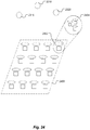
- Fig. 14 is a schematic top view of one binary optical switch 1400 of the second binary optical switches 1228-1242.
- the binary optical switch 1400 includes a translatable grating 1402.
- the translatable grating 1402 defines a plurality of parallel or approximately parallel periodic grooves.
- the grooves are separated by walls, represented by walls 1404, 1406 and 1408.
- the grooves and walls may be implemented by respective materials having different refractive indexes.
- the walls 1404-1408 may be made of silicon, silicon nitride or another suitable material using conventional semiconductor fabrication techniques.
- the grooves may be voids or made of a suitable material different from the walls 1404-1408.
- the translatable grating 1402 is shown with six walls 1404-1408, any suitable number of walls and/or grooves may be used.
- the translatable grating 1402 is disposed above a second optical waveguide 1410, one of the second optical waveguides 1208-1216 ( Fig. 12 ).
- Fig. 15 is a schematic side view of the binary optical switch 1400 in the OFF position.
- the translatable optical grating 1402 is disposed a distance 1500 from the second optical waveguide 1410 sufficient to optically couple with the second optical waveguide 1410 with a coupling efficiency of at most about 5%, preferably less than 1%, and in some embodiments less than 0.1%.
- the distance 1500 is about 1 ⁇ m (1,000 nm).
- the distance 1500 may be about 800 nm.
- the distance 1500 may be about 250 nm.
- most or substantially all light 1502 in the second optical waveguide 1410 continues along the second optical waveguide 1410, as indicated by an arrow 1504. Similarly, very little or substantially no light from free space couples via the optical grating 1402 into the second optical waveguide 1410.
- the second optical waveguide 1410 may be fabricated using conventional semiconductor fabrication techniques on a suitable semiconductor wafer, such as a silicon or silicon nitride wafer.
- the second optical waveguide 1410 may be fabricated on a suitable oxide or other passivation layer 1506.
- Fig. 16 is a schematic side view of the binary optical switch 1400 in the ON position.
- the translatable optical grating 1402 In the ON position, the translatable optical grating 1402 is disposed a distance 1600 from the second optical waveguide 1410 sufficient to optically couple with the second optical waveguide 1410 with a coupling efficiency of at least about 25%. In some embodiments, the distance 1600 is about 10-50 nm.
- the ON position much, most or substantially all light 1502 in the second optical waveguide 1410 is emitted by the translatable optical grating 1402 into free space, as indicated by an arrow 1602. Similarly, much, most or substantially all light of a suitable mode from free space couples via the optical grating 1402 into the second optical waveguide 1410.
- Fig. 17 is another schematic side view of the binary optical switch 1400 in the ON position showing representative dimensions, according to an embodiment of the present invention.
- the translatable grating 1402 is disposed a distance (D) about 20 nm from the second optical waveguide 1410.
- the second optical waveguide 1410 is about 150 nm thick (T) silicon on an oxide substrate 1506.
- the input light beam 1502 is a Gaussian with an about 2.5 ⁇ m radius.
- the translatable grating 1402 is about 50 nm thick (H).
- the translatable grating 1402 has a groove period (A) of about 580 nm. Appropriate modifications may be made, such as changing the groove period (A) for other wavelengths of light, as would be known by one of ordinary skill in the art.
- each second optical switch 1228-1242 may include a MEMS structure that is configured to selectively translate the translatable optical grating 1402 to the ON position and to the OFF position.
- Figs. 18 and 19 are respective schematic perspective and side views of the optical switch 1400 in the OFF position, showing an electrostatic MEMS structure 1800 configured to selectively translate the translatable optical grating 1400 to the ON position and to the OFF position.
- Fig. 20 is a schematic perspective side view of the optical switch 1400 in the ON position.
- the translatable optical grating 1402 is shown within a dashed ellipse 1802.
- the translatable optical grating 1402 is part of a bridge 1804.
- the bridge 1804 is spaced apart from, and disposed above, the substrate 1506.
- the substrate 1506 may include a buried oxide layer 1900 ( Figs. 19 and 20 ).
- the bridge 1804 is supported by respective piers 1808 and 1810.
- the second optical waveguide 1410 is disposed in or on the substrate 1506 under the translatable optical grating 1402.
- the bridge 1804 includes two first electrostatic actuation electrodes 1812 and 1814. Two corresponding second electrostatic actuation electrodes 1816 and 1818 are disposed on the substrate 1506, such that the two first actuation electrodes 1812 and 1814 register over the two second actuation electrodes 1816 and 1818, respectively.
- the bridge 1804 also includes two flexures 1820 and 1822.
- a resulting electrostatic force urges the first actuation electrodes 1812-1814 and the translatable optical grating 1402 toward the substrate 1506, thereby bringing the translatable optical grating 1402 within an appropriate distance of the second optical waveguide 1410 to turn the optical switch 1400 ON. Absent such an electric potential and the resulting electrostatic force, the flexures 1820 and 1822 return the translatable optical grating 1402 to the OFF position.
- a boss 1902 ( Fig. 19 ) may be included to limit travel distance of the translatable optical grating 1402 in the ON position.
- Other aspects of the MEMS structure 1800 are similar to MEMS structures described in Seok and Seok supplement.
- Figs. 21 and 22 contain graphs 2100 and 2200 illustrating results of computer modeled E-field strength versus z-x location within the optical switch 1400 in the ON and OFF positions, respectively.
- the second optical waveguide 1410 is vertical, and light travels down the second optical waveguide 1410, as indicated by arrows 2102.
- light that couples into the translatable grating 1402 and exits the switch 1400 is indicated by an arrow 2104.
- the light wavelength is 1.5-1.6 ⁇ m
- the E-field strength is color coded 2106.
- the translatable grating 1402 is disposed 20 nm from the second optical waveguide 1410, whereas for the plot 2200 (optical switch 1400 OFF), the translatable grating 1402 is disposed 250 nm from the second optical waveguide 1410.
- a relatively small number, such as one each, of the first and second optical switches 1218-1226 and 1228-1242 needs to be operated, i.e., ON, to route an optical signal from the common input/output port 1202 to the selected port 1238
- This small number of switches therefore consumes much less energy than phase shifters in a comparable optical phased array.
- the MEMS-based first and second optical switches 1218-1226 and 1228-1242 may be smaller, and may therefore be fabricated or packed more densely, than phase shifters or binary optical switches of an H-tree.
- the first and second optical switches 1218-1226 and 1228-1242 fully direct the light down one path or another.
- the optical switch network 1200 ( Fig. 12 ) is partitioned into multiple optical switch networks, each operating independently and each handling a non-overlapping subset of the N ports 202-210. This is similar to including multiple optical switches 104 in the optical transmit/receive terminal 100 ( Fig. 1 ).
- Multiple optical switch networks 104, or a partitioned optical switch network 104 can handle multiple diverse light rays 106, i.e., each light ray 106 being directed in a different direction is space.
- Fig. 23 is a schematic diagram of a display projector 2300 capable of projecting an image that is perceived differently by viewers observing the projection from different angles.
- An optical switch network 2302 such as any of the optical switch networks described herein, receives light via an optical input 2304, such as from a modulated laser (not shown), and routes the light to an output port of a plurality of output ports 2306, as directed by a controller 2308.
- Each output port 2306 may be an optical coupler, such as described herein.
- the controller may use data from a data source 2310 to command the optical switch network 2302.
- the data source 2310 may contain predefined data or the data may be generated in real time.
- the data source 2310 may contain data defining, for example, a 3-dimensional representation of an object.
- a lenticular lens 2312 optically couples the output ports 2306 to free space 2314. Due to the nature of the lenticular lens 2312, each observation angle, represented by observers 2316, 2318 and 2320, sees a different portion of the output ports 2306. Specifically, each observer 2316-2320 sees a different output port of the output ports 2306, as indicated by lines 2322, 2324 and 2326.
- the display projector 2300 may project one pixel of an image, and each observer 2300 may see that pixel differently, based on the observer's position, relative to the lenticular lens 2312.
- the pixel may represent a portion of a flower. That portion of the flower would appear different to different observers observing the flower from different locations. For example, if the portion of the flower is illuminated, and an observer's line of sight to the portion of the flower is not blocked, the observer would see the portion of the flower. However, if the observer's line of sight is blocked, the portion of the flower would be invisible. Similarly, the portion of the flower may appear elongated or compressed, depending on the angle of observation. Thus, depending on the observer's angle, a given pixel may be bright, dim or blank (invisible).
- the display projector 2300 may include a set 2400 of optical switch networks, output ports and lenticular lens, one optical switch network, one output port and one lenticular lens for each pixel to be projected, as schematically illustrated in Fig. 24 .
- the respective pixels represented by the set 2400 of optical switch networks, output ports and lenticular arrays are tiled to form a multi-pixel image.
- Each optical switch network, output port and lenticular array group, represented by group 2402 may project a single color, such as white or red, to form a monochrome image.
- each group 2402 may include three optical switch networks, three output ports and three lenticular lenses, as shown at 2404, where each optical switch network, output port and lenticular lens projects a different color, such as red, green and blue.
- the controller 2308 may scan through the output ports 2306, i.e., through the possible view angles, to project a different amplitude and/or color for each view angle.
- the controller 2308 may modulate a light source 2328 to control the amplitude and/or color of the input light 2304. If the light source 2328 is capable of projecting red, green and blue, or another suitable range of colors, the controller 2308 may cycle through the colors for each output port 2306 and thereby project a color image to the observers 2316-2320. In any case, the scanning should be done quickly enough that the observers 2316-2320 do not perceive flicker.
- the display projector 2300 is described as having a separate lenticular lens for each pixel, a single lenticular lens may be large enough to project several pixels, such as all or some of the pixels in a given column.
- a lenslet array of lenticular lenses may be used.
- Fig. 25 is a schematic illustration of another embodiment of an optical switch network 2500, according to an embodiment of the present invention.
- the optical switch network 2500 includes a wavelength filter 2502, such as a prism.
- the wavelength filter 2502 directs the light to one of the output ports 2306.
- the source of the input light 2304 may be, for example, a tunable laser 2504, and a controller 2506 may control the wavelength of the tunable laser 2504, based on information from the data source 2310, to select which output port 2306 is to project light.
- the controller 2506 may scan through the wavelengths and modulate the amplitude of the tunable laser 2504 to affect the amplitude of the pixel projected at each angle, i.e. to the observers 2316-2320.
- the output ports 2306 pass the wavelength of light they receive. In other embodiments, the output ports 2306 are configured to be stimulated by the incoming light, regardless of wavelength, and emit a predetermined wavelength of light, such as red, green or blue.
- optical switch network 2500 may be used to project monochrome pixels. If color pixels are to be projected, the scheme described with respect to Fig. 25 may be replicated for each pixel, and each replica may project a different color, such as red, green and blue, as discussed with respect to group 2404 ( Fig. 24 ).
- the wavelength filter 2502 is different, so as to enable three suitable different colors, such as red, green and blue, to reach a given output port 2306 in each replica, where the three colors can be used in combination to be perceived by a human observer 2316-2320 as a given color.
- the wavelength filter 2502 in one of three replicas may be configured such that red light reaches a given output port 2306 in the replica
- the wavelength filter 2502 in a second of the three replicas may be configured such that green light reaches the corresponding, i.e., same output direction, output port 2306 in the second replica
- the wavelength filter 2502 in a third of the three replicas may be configured such that blue light reaches the corresponding, i.e., same output direction, output port 2306 in the third replica.
- the scheme described with respect to Fig. 25 may be replicated for each pixel, as discussed above.
- the wavelength filter 2502 is different, so as to enable three suitable different colors, such as red, green and blue, to reach a given output port 2306 in each replica, where the three colors can be used in combination to be perceived by a human observer 2316-2320 as a given color.
- the wavelength filter 2502 in one of three replicas may be configured such that red light reaches a given output port 2306 in the replica
- the wavelength filter 2502 in a second of the three replicas may be configured such that yellow light reaches the corresponding, i.e., same output direction, output port 2306 in the second replica
- the wavelength filter 2502 in a third of the three replicas may be configured such that orange light reaches the corresponding, i.e., same output direction, output port 2306 in the third replica.
- this scheme may limit the range or number of colors that are projectable to each observer 2316-2320.
- the observers 2316-2320 may be replaced by optical sources, such as light reflected from objects, and the light source 2328 and the tunable laser 2504 may be replaced by suitable optical receivers to form receive terminals.
- optical coupler means an optical antenna or other interface device between optical signals traveling in free space and optical signals traveling in a waveguide, such as an optical fiber or solid glass.
- ports 200 discussed with reference to Figs. 2 and 12 may be implemented with optical couplers.
- an optical coupler should facilitate this change of direction.
- Examples of optical couplers include compact gratings, prisms fabricated in waveguides and facets etched in wafers and used as mirrors.
- An optical antenna is a device designed to efficiently convert free-propagating optical radiation to localized energy, and vice versa. Optical antennas are described by Palash Bharadwaj, et al., "Optical Antennas," Advances in Optics and Photonics 1.3 (2009), pp. 438-483.
- the optical switch network 104 or 1200 may be implemented on a photonic chip, such as a silicon waver.
- a photonic chip such as a silicon waver.
- “Wafer” means a manufactured substrate, such as a silicon wafer. The surface of the earth, for example, does not fall within the meaning of wafer.
- the photonic chip provides a substrate, and the photonic chip may be fabricated to provide optical waveguides within a thickness of the substrate.
- the optical waveguides may be made of glass or another material that is optically transparent at wavelengths of interest.
- the optical waveguides may be solid or they may be hollow, such as a hollow defined by a bore in the thickness of the substrate, and partially evacuated or filled with gas, such as air or dry nitrogen.
- the optical waveguides may be defined by a difference in refractive index of the optical medium of the waveguides and refractive index of the substrate or other material surrounding the optical waveguides.
- the photonic chip may be fabricated using conventional semiconductor fabrication processes, such as the conventional CMOS process.
- passive waveguides can be made of a variety of well-known materials, preferably silicon nitride, because of its compatibility with CMOS fabrication processes and high index contrast.
- Alternative materials for passive waveguides include doped silica or polymers.
- Active materials include GaN, A1N, and certain polymers.
- light means electromagnetic radiation having a wavelength between about 100 nm and about 1 mm.
- the term "and/or,” used in connection with a list of items, including in the claims, means one or more of the items in the list, i.e., at least one of the items in the list, but not necessarily all the items in the list.
- the term "or,” used in connection with a list of items means one or more of the items in the list, i.e., at least one of the items in the list, but not necessarily all the items in the list. "Or” does not mean "exclusive or.”
- an element described as being configured to perform an operation "or" another operation is met by an element that is configured to perform only one of the operations. That is, the element need not be configured operate in one mode in which it performs one of the operations, and in another mode in which it performs the other operation.
- the element may, but need not, be configured to perform more than one of the operations.
- each block or combination of blocks may be combined, separated into separate operations or performed in other orders. All or a portion of each block or combination thereof may be implemented as computer program instructions (such as software), hardware (such as combinatorial logic, Application Specific Integrated Circuits (ASICs), Field-Programmable Gate Arrays (FPGAs), processor or other hardware), firmware or combinations thereof.
- ASICs Application Specific Integrated Circuits
- FPGAs Field-Programmable Gate Arrays
- selecting a direction in which to transmit or receive light by a transmit/receive terminal 100 may be performed by a processor executing instructions stored in a memory.
- Embodiments, or portions thereof, may be implemented by one or more processors executing, or controlled by, instructions stored in a memory.
- Each processor may be a general purpose processor, such as a central processing unit (CPU), a graphic processing unit (GPU), digital signal processor (DSP), a special purpose processor, etc., as appropriate, or combination thereof.
- CPU central processing unit
- GPU graphic processing unit
- DSP digital signal processor
- the memory may be random access memory (RAM), read-only memory (ROM), flash memory or any other memory, or combination thereof, suitable for storing control software or other instructions and data.
- Instructions defining the functions of the present invention may be delivered to a processor in many forms, including, but not limited to, information permanently stored on tangible non-writable storage media (e.g., read-only memory devices within a computer, such as ROM, or devices readable by a computer I/O attachment, such as CD-ROM or DVD disks), information alterably stored on tangible writable storage media (e.g., floppy disks, removable flash memory and hard drives) or information conveyed to a computer through a communication medium, including wired or wireless computer networks.
- tangible non-writable storage media e.g., read-only memory devices within a computer, such as ROM, or devices readable by a computer I/O attachment, such as CD-ROM or DVD disks
- information alterably stored on tangible writable storage media e.
Landscapes
- Physics & Mathematics (AREA)
- Engineering & Computer Science (AREA)
- General Physics & Mathematics (AREA)
- Computer Networks & Wireless Communication (AREA)
- Optics & Photonics (AREA)
- Radar, Positioning & Navigation (AREA)
- Remote Sensing (AREA)
- Microelectronics & Electronic Packaging (AREA)
- Computer Hardware Design (AREA)
- Astronomy & Astrophysics (AREA)
- Spectroscopy & Molecular Physics (AREA)
- Signal Processing (AREA)
- Electromagnetism (AREA)
- Mechanical Light Control Or Optical Switches (AREA)
- Optical Modulation, Optical Deflection, Nonlinear Optics, Optical Demodulation, Optical Logic Elements (AREA)
- Optical Communication System (AREA)
- Micromachines (AREA)
Applications Claiming Priority (4)
| Application Number | Priority Date | Filing Date | Title |
|---|---|---|---|
| US201662498158P | 2016-12-16 | 2016-12-16 | |
| US201762450855P | 2017-01-26 | 2017-01-26 | |
| US201762516602P | 2017-06-07 | 2017-06-07 | |
| PCT/US2017/066885 WO2018112447A1 (en) | 2016-12-16 | 2017-12-16 | Integrated mems switches for selectively coupling light in and out of a waveguide |
Publications (2)
| Publication Number | Publication Date |
|---|---|
| EP3555681A1 EP3555681A1 (en) | 2019-10-23 |
| EP3555681B1 true EP3555681B1 (en) | 2021-04-14 |
Family
ID=60972390
Family Applications (2)
| Application Number | Title | Priority Date | Filing Date |
|---|---|---|---|
| EP17829428.6A Active EP3555681B1 (en) | 2016-12-16 | 2017-12-16 | Optical switch network |
| EP17833029.6A Active EP3555682B1 (en) | 2016-12-16 | 2017-12-16 | All-solid state opticaltransmit/receive terminal |
Family Applications After (1)
| Application Number | Title | Priority Date | Filing Date |
|---|---|---|---|
| EP17833029.6A Active EP3555682B1 (en) | 2016-12-16 | 2017-12-16 | All-solid state opticaltransmit/receive terminal |
Country Status (6)
| Country | Link |
|---|---|
| US (3) | US10739520B2 (enExample) |
| EP (2) | EP3555681B1 (enExample) |
| JP (3) | JP6880190B2 (enExample) |
| KR (2) | KR102251273B1 (enExample) |
| CA (1) | CA3041101C (enExample) |
| WO (2) | WO2018112447A1 (enExample) |
Families Citing this family (50)
| Publication number | Priority date | Publication date | Assignee | Title |
|---|---|---|---|---|
| KR102251273B1 (ko) * | 2016-12-16 | 2021-05-14 | 더 차레스 스타크 드레이퍼 래보레이토리, 인코포레이티드 | 전 고체 광학 송/수신 단말기 |
| EP3635460B1 (en) * | 2017-06-07 | 2021-12-08 | The Charles Stark Draper Laboratory, Inc. | Integrated mems switches for selectively coupling light in and out of a waveguide |
| WO2019099470A1 (en) * | 2017-11-14 | 2019-05-23 | The Charles Stark Draper Laboratory, Inc. | Foveal patterned optical switches for mems lidar beam steering unit |
| US10838150B2 (en) | 2017-11-28 | 2020-11-17 | The Charles Stark Draper Laboratory, Inc. | Coupling lens aberration correction through grating design in a switched focal plane array |
| US10156770B1 (en) * | 2018-02-08 | 2018-12-18 | The Charles Stark Draper Laboratory, Inc. | Packaging and interconnect systems for edge-emitting light modulators based on surface acoustic wave (SAW) modulation |
| US10908372B2 (en) * | 2018-03-05 | 2021-02-02 | The Charles Stark Draper Laboratory, Inc. | Systems and methods for isolating excitation and signal paths for chip-scale LIDAR |
| US10848152B2 (en) | 2018-03-15 | 2020-11-24 | Analog Devices Global Unlimited Company | Optically isolated micromachined (MEMS) switches and related methods comprising a light transmitting adhesive layer between an optical receiver and a light source |
| US11441353B2 (en) * | 2018-06-19 | 2022-09-13 | The Regents Of The University Of California | Beam-steering system based on a MEMS-actuated vertical-coupler array |
| US11536805B2 (en) | 2018-06-25 | 2022-12-27 | Silc Technologies, Inc. | Optical switching for tuning direction of LIDAR output signals |
| US20200116842A1 (en) * | 2018-10-12 | 2020-04-16 | Silc Technologies, Inc. | Optical switching in lidar systems |
| WO2020087016A1 (en) * | 2018-10-26 | 2020-04-30 | The Charles Stark Draper Laboratory, Inc. | Adaptive lidar scanning techniques for improved frame rate and safety |
| WO2020097574A2 (en) | 2018-11-09 | 2020-05-14 | The Charles Stark Draper Laboratory, Inc. | Dual-polarization lidar systems and methods |
| DE102018222721A1 (de) | 2018-12-21 | 2020-06-25 | Robert Bosch Gmbh | LIDAR-Sensor für ein LIDAR-System |
| GB2583172B (en) * | 2019-02-06 | 2023-09-13 | Rockley Photonics Ltd | Optical components for imaging |
| US12429569B2 (en) | 2019-05-17 | 2025-09-30 | Silc Technologies, Inc. | Identification of materials illuminated by LIDAR systems |
| CN110233677A (zh) * | 2019-05-20 | 2019-09-13 | 电子科技大学 | 一种基于光正交码的激光通信测距装置及方法 |
| US11650317B2 (en) | 2019-06-28 | 2023-05-16 | Silc Technologies, Inc. | Use of frequency offsets in generation of LIDAR data |
| US11906785B2 (en) * | 2019-07-01 | 2024-02-20 | University Of Central Florida Research Foundation, Inc. | Photonic integrated circuit outcoupling array for imaging-based beam steering |
| CN110333511B (zh) * | 2019-07-22 | 2021-10-22 | 西安知微传感技术有限公司 | 一种收发同步激光雷达光学系统 |
| CN112444916B (zh) * | 2019-08-27 | 2024-02-02 | 新加坡国立大学 | 多层波导装置及其制造方法 |
| US10823913B1 (en) | 2019-09-27 | 2020-11-03 | The Charles Stark Draper Laboratory, Inc. | Optical switch controllable by vertical motion MEMS structure |
| US11237335B1 (en) | 2019-09-27 | 2022-02-01 | The Charles Stark Draper Laboratory, Inc. | Optical switch controllable by vertical motion MEMS structure |
| EP4231089A3 (en) * | 2019-11-12 | 2024-03-13 | Pointcloud Inc. | Dual path light detection and ranging system |
| US11953625B2 (en) * | 2020-01-27 | 2024-04-09 | The Charles Stark Draper Laboratory, Inc. | Beamsplitter architecture for monostatic LiDAR |
| EP3907525B1 (en) | 2020-05-05 | 2023-07-05 | The Charles Stark Draper Laboratory, Inc. | Multi-mode signal lidar collection methods and systems |
| US11428785B2 (en) * | 2020-06-12 | 2022-08-30 | Ours Technology, Llc | Lidar pixel with active polarization control |
| US20220003842A1 (en) * | 2020-07-02 | 2022-01-06 | Robert Bosch Gmbh | Lidar Module With Monolithic Array |
| DE102021206988A1 (de) * | 2020-07-02 | 2022-01-05 | Robert Bosch Gesellschaft mit beschränkter Haftung | Mems-schalter für die optische kopplung |
| US11307483B2 (en) | 2020-07-02 | 2022-04-19 | Robert Bosch Gmbh | MEMS optical switch with dual cantilever couplers |
| US11360270B2 (en) | 2020-07-02 | 2022-06-14 | Robert Bosch Gmbh | MEMS optical switch with stop control |
| US11340399B2 (en) | 2020-07-02 | 2022-05-24 | Robert Bosch Gmbh | In-plane MEMS optical switch |
| CN115867840A (zh) * | 2020-07-10 | 2023-03-28 | 沃扬光电公司 | 发射器阵列 |
| US11699862B2 (en) | 2020-08-21 | 2023-07-11 | The Charles Stark Draper Laboratory, Inc. | Two-dimensional planar and crossover-free beamforming network architecture |
| CN112305676B (zh) * | 2020-09-23 | 2021-10-08 | 浙江大学 | 基于静电梳驱动的硅基mems光开关及n×n阵列 |
| CN114280575B (zh) * | 2020-09-27 | 2025-11-11 | 北京万集科技股份有限公司 | 一种基于微环光开关网络的激光雷达光学芯片 |
| WO2022103997A1 (en) * | 2020-11-15 | 2022-05-19 | Naiqian Han | Optical mems based intracranial pressure and intracranial temperature monitor |
| US20210133547A1 (en) * | 2020-11-17 | 2021-05-06 | Intel Corporation | High efficiency optical neural network |
| DE102020214458A1 (de) | 2020-11-18 | 2022-05-19 | Robert Bosch Gesellschaft mit beschränkter Haftung | Scanvorrichtung zum Aussenden von Lichtstrahlen einer Lichtquelle und/oder zum Abbilden von Lichtstrahlen auf einen Detektor, LiDAR-Sensor und Verfahren zur Ansteuerung einer Scanvorrichtung |
| KR102799813B1 (ko) * | 2021-01-26 | 2025-04-25 | 재단법인대구경북과학기술원 | 멀티캐스트 스위치 어레이 및 이를 이용한 빔 조향 장치 |
| WO2022164206A1 (ko) * | 2021-01-26 | 2022-08-04 | 재단법인대구경북과학기술원 | 멀티캐스트 스위치 어레이 및 이를 이용한 빔 조향 장치 |
| CN114859623B (zh) * | 2021-02-05 | 2024-10-29 | 联合微电子中心有限责任公司 | 三维光开关、三维光网络和三维光芯片 |
| WO2022192539A1 (en) * | 2021-03-10 | 2022-09-15 | Neophotonics Corporation | Lidar with 4d object classification, solid state optical scanning arrays, and effective pixel designs |
| KR20220144700A (ko) * | 2021-04-20 | 2022-10-27 | 삼성전자주식회사 | 복수의 스위치를 포함하는 라이다 장치 |
| CN117425837A (zh) | 2021-05-10 | 2024-01-19 | 奈伊系统公司 | 具有二维硅光子MEMS开关阵列的伪单站LiDAR |
| CN117597603A (zh) | 2021-05-19 | 2024-02-23 | 尼亚系统有限公司 | 具有微透镜阵列及集成光子开关阵列的lidar |
| EP4341733B1 (fr) * | 2021-09-06 | 2024-07-31 | Airbus Defence and Space SAS | Structure pour collecter de la lumiere |
| US12411213B2 (en) | 2021-10-11 | 2025-09-09 | Silc Technologies, Inc. | Separation of light signals in a LIDAR system |
| US11982748B2 (en) | 2022-01-20 | 2024-05-14 | Silc Technologies, Inc. | Imaging system having multiple cores |
| US12066541B2 (en) | 2022-01-20 | 2024-08-20 | Silc Technologies, Inc. | Imaging system having multiple cores |
| US12422618B2 (en) | 2022-10-13 | 2025-09-23 | Silc Technologies, Inc. | Buried taper with reflecting surface |
Family Cites Families (29)
| Publication number | Priority date | Publication date | Assignee | Title |
|---|---|---|---|---|
| US4013000A (en) | 1975-11-20 | 1977-03-22 | Bell Telephone Laboratories, Incorporated | Optical crossbar switching network |
| US5059008A (en) | 1990-03-26 | 1991-10-22 | General Electric Company | Wide angle beam steerer using translation of plural lens arrays |
| US5392157A (en) | 1993-08-18 | 1995-02-21 | Trw Inc. | Line-of-sight steering system for high power laser beams and method using same |
| US5757536A (en) * | 1995-08-30 | 1998-05-26 | Sandia Corporation | Electrically-programmable diffraction grating |
| US5943159A (en) | 1996-05-14 | 1999-08-24 | Zhu; Tom Yuxin | Method and apparatus for optical beam steering |
| US6341118B1 (en) * | 1998-06-02 | 2002-01-22 | Science Applications International Corporation | Multiple channel scanning device using oversampling and image processing to increase throughput |
| US7003187B2 (en) * | 2000-08-07 | 2006-02-21 | Rosemount Inc. | Optical switch with moveable holographic optical element |
| US6597829B2 (en) * | 2001-04-27 | 2003-07-22 | Robert H. Cormack | 1xN optical fiber switch |
| CN100445798C (zh) | 2001-07-13 | 2008-12-24 | 柔斯芒特公司 | 具有可移动的全息光学元件的光开关 |
| US7298555B2 (en) | 2001-12-07 | 2007-11-20 | The Boeing Company | Optical beam steering using small angle beam steering device |
| US6608715B2 (en) * | 2001-12-10 | 2003-08-19 | Integrated Optics Communications Corporation | Wavelength converter using Bragg-grating |
| AU2003220012A1 (en) | 2002-03-01 | 2003-09-16 | Rosemount Inc. | Optical switch with 3d waveguides |
| WO2003098263A2 (en) * | 2002-05-17 | 2003-11-27 | Arete Associates | Imaging lidar with micromechanical components |
| US6927886B2 (en) | 2002-08-02 | 2005-08-09 | Massachusetts Institute Of Technology | Reconfigurable image surface holograms |
| JP2005172850A (ja) | 2003-12-05 | 2005-06-30 | Nippon Sheet Glass Co Ltd | 光クロスコネクト装置およびその調整方法 |
| US7864419B2 (en) | 2004-06-08 | 2011-01-04 | Ellis Amalgamated LLC | Optical scanning assembly |
| US7095925B2 (en) | 2004-11-03 | 2006-08-22 | Intel Corporation | Optical phased array transmitter/receiver |
| US7936448B2 (en) * | 2006-01-27 | 2011-05-03 | Lightwire Inc. | LIDAR system utilizing SOI-based opto-electronic components |
| US7556389B2 (en) | 2006-03-30 | 2009-07-07 | Raytheon Company | Pointable optical system with coude optics having a short on-gimbal path length |
| JP2008090075A (ja) | 2006-10-03 | 2008-04-17 | Toshiba Corp | 半導体集積回路 |
| US8867868B2 (en) | 2006-10-03 | 2014-10-21 | Kabushiki Kaisha Toshiba | Semiconductor integrated circuit |
| DE102007039019A1 (de) | 2007-07-03 | 2009-01-15 | Diehl Bgt Defence Gmbh & Co. Kg | Vorrichtung zum Schwenken eines optischen Strahls |
| CN102884444B (zh) | 2010-05-07 | 2014-08-13 | 三菱电机株式会社 | 激光雷达装置 |
| US8988754B2 (en) * | 2013-01-08 | 2015-03-24 | Massachusetts Institute Of Technology | Optical phased arrays with evanescently-coupled antennas |
| US9476981B2 (en) | 2013-01-08 | 2016-10-25 | Massachusetts Institute Of Technology | Optical phased arrays |
| JP6017380B2 (ja) | 2013-07-16 | 2016-11-02 | 日本電信電話株式会社 | 1×n光スイッチ素子及びn×n光スイッチ素子 |
| WO2015147966A2 (en) | 2014-01-11 | 2015-10-01 | The Regents Of The University Of California | Silicon-photonics-based optical switch |
| WO2017058322A2 (en) | 2015-06-30 | 2017-04-06 | Massachusetts Institute Of Technology | Apparatus and methods for augmented reality |
| KR102251273B1 (ko) * | 2016-12-16 | 2021-05-14 | 더 차레스 스타크 드레이퍼 래보레이토리, 인코포레이티드 | 전 고체 광학 송/수신 단말기 |
-
2017
- 2017-12-16 KR KR1020197017638A patent/KR102251273B1/ko active Active
- 2017-12-16 CA CA3041101A patent/CA3041101C/en active Active
- 2017-12-16 JP JP2019529186A patent/JP6880190B2/ja active Active
- 2017-12-16 EP EP17829428.6A patent/EP3555681B1/en active Active
- 2017-12-16 WO PCT/US2017/066885 patent/WO2018112447A1/en not_active Ceased
- 2017-12-16 EP EP17833029.6A patent/EP3555682B1/en active Active
- 2017-12-16 KR KR1020197017690A patent/KR20190093200A/ko not_active Ceased
- 2017-12-16 WO PCT/US2017/000095 patent/WO2018111316A1/en not_active Ceased
- 2017-12-16 US US15/732,693 patent/US10739520B2/en active Active
- 2017-12-16 JP JP2019529194A patent/JP7133552B2/ja active Active
- 2017-12-16 US US15/844,527 patent/US10473862B2/en active Active
-
2019
- 2019-10-09 US US16/597,595 patent/US10684420B2/en active Active
-
2020
- 2020-11-05 JP JP2020185002A patent/JP2021012401A/ja not_active Withdrawn
Non-Patent Citations (1)
| Title |
|---|
| None * |
Also Published As
| Publication number | Publication date |
|---|---|
| CA3041101A1 (en) | 2018-06-21 |
| CA3041101C (en) | 2021-06-22 |
| JP7133552B2 (ja) | 2022-09-08 |
| US20180172918A1 (en) | 2018-06-21 |
| WO2018111316A1 (en) | 2018-06-21 |
| US20180175961A1 (en) | 2018-06-21 |
| KR20190084311A (ko) | 2019-07-16 |
| JP6880190B2 (ja) | 2021-06-02 |
| WO2018112447A1 (en) | 2018-06-21 |
| KR20190093200A (ko) | 2019-08-08 |
| JP2020504834A (ja) | 2020-02-13 |
| KR102251273B1 (ko) | 2021-05-14 |
| EP3555681A1 (en) | 2019-10-23 |
| US10739520B2 (en) | 2020-08-11 |
| EP3555682B1 (en) | 2024-04-10 |
| JP2019537068A (ja) | 2019-12-19 |
| US20200041728A1 (en) | 2020-02-06 |
| US10473862B2 (en) | 2019-11-12 |
| EP3555682A1 (en) | 2019-10-23 |
| JP2021012401A (ja) | 2021-02-04 |
| US10684420B2 (en) | 2020-06-16 |
Similar Documents
| Publication | Publication Date | Title |
|---|---|---|
| US10684420B2 (en) | Integrated MEMS switches for selectively coupling light in and out of a waveguide | |
| US10466423B2 (en) | Partitioned optical switch | |
| US11781379B2 (en) | Beam-steering system based on a MEMS-actuated vertical-coupler array | |
| US11428811B2 (en) | Foveal patterned optical switches for MEMS LiDAR beam steering unit | |
| EP2902826B1 (en) | 2x2 wavelength selective switch array | |
| US20210293934A1 (en) | Switched optical phased array based beam steering lidar | |
| US11762062B2 (en) | Multi-mode signal LiDAR collection methods and systems | |
| US8693819B2 (en) | Method and system for switching optical channels | |
| CN109738988B (zh) | 基于透镜的全固态水平二维光束转向装置 | |
| Spector | Review of lens-assisted beam steering methods | |
| US11906785B2 (en) | Photonic integrated circuit outcoupling array for imaging-based beam steering | |
| US20060034567A1 (en) | Optical beam combiner | |
| RU2088960C1 (ru) | Многокаскадный оптоэлектронный коммутатор | |
| JP2018124402A (ja) | 光入出力装置 | |
| Paek et al. | 2D multiple beam steering with acoustically steered and rotated (ASTRO) true-time delay generator | |
| JPH03208012A (ja) | 光信号伝達方法 |
Legal Events
| Date | Code | Title | Description |
|---|---|---|---|
| STAA | Information on the status of an ep patent application or granted ep patent |
Free format text: STATUS: UNKNOWN |
|
| STAA | Information on the status of an ep patent application or granted ep patent |
Free format text: STATUS: THE INTERNATIONAL PUBLICATION HAS BEEN MADE |
|
| PUAI | Public reference made under article 153(3) epc to a published international application that has entered the european phase |
Free format text: ORIGINAL CODE: 0009012 |
|
| STAA | Information on the status of an ep patent application or granted ep patent |
Free format text: STATUS: REQUEST FOR EXAMINATION WAS MADE |
|
| 17P | Request for examination filed |
Effective date: 20190614 |
|
| AK | Designated contracting states |
Kind code of ref document: A1 Designated state(s): AL AT BE BG CH CY CZ DE DK EE ES FI FR GB GR HR HU IE IS IT LI LT LU LV MC MK MT NL NO PL PT RO RS SE SI SK SM TR |
|
| AX | Request for extension of the european patent |
Extension state: BA ME |
|
| STAA | Information on the status of an ep patent application or granted ep patent |
Free format text: STATUS: EXAMINATION IS IN PROGRESS |
|
| 17Q | First examination report despatched |
Effective date: 20200124 |
|
| DAV | Request for validation of the european patent (deleted) | ||
| DAX | Request for extension of the european patent (deleted) | ||
| GRAP | Despatch of communication of intention to grant a patent |
Free format text: ORIGINAL CODE: EPIDOSNIGR1 |
|
| STAA | Information on the status of an ep patent application or granted ep patent |
Free format text: STATUS: GRANT OF PATENT IS INTENDED |
|
| INTG | Intention to grant announced |
Effective date: 20201029 |
|
| GRAS | Grant fee paid |
Free format text: ORIGINAL CODE: EPIDOSNIGR3 |
|
| GRAA | (expected) grant |
Free format text: ORIGINAL CODE: 0009210 |
|
| STAA | Information on the status of an ep patent application or granted ep patent |
Free format text: STATUS: THE PATENT HAS BEEN GRANTED |
|
| AK | Designated contracting states |
Kind code of ref document: B1 Designated state(s): AL AT BE BG CH CY CZ DE DK EE ES FI FR GB GR HR HU IE IS IT LI LT LU LV MC MK MT NL NO PL PT RO RS SE SI SK SM TR |
|
| REG | Reference to a national code |
Ref country code: GB Ref legal event code: FG4D |
|
| REG | Reference to a national code |
Ref country code: CH Ref legal event code: EP |
|
| REG | Reference to a national code |
Ref country code: DE Ref legal event code: R096 Ref document number: 602017036828 Country of ref document: DE |
|
| REG | Reference to a national code |
Ref country code: IE Ref legal event code: FG4D |
|
| REG | Reference to a national code |
Ref country code: AT Ref legal event code: REF Ref document number: 1382950 Country of ref document: AT Kind code of ref document: T Effective date: 20210515 |
|
| REG | Reference to a national code |
Ref country code: LT Ref legal event code: MG9D |
|
| REG | Reference to a national code |
Ref country code: AT Ref legal event code: MK05 Ref document number: 1382950 Country of ref document: AT Kind code of ref document: T Effective date: 20210414 |
|
| REG | Reference to a national code |
Ref country code: NL Ref legal event code: MP Effective date: 20210414 |
|
| PG25 | Lapsed in a contracting state [announced via postgrant information from national office to epo] |
Ref country code: FI Free format text: LAPSE BECAUSE OF FAILURE TO SUBMIT A TRANSLATION OF THE DESCRIPTION OR TO PAY THE FEE WITHIN THE PRESCRIBED TIME-LIMIT Effective date: 20210414 Ref country code: LT Free format text: LAPSE BECAUSE OF FAILURE TO SUBMIT A TRANSLATION OF THE DESCRIPTION OR TO PAY THE FEE WITHIN THE PRESCRIBED TIME-LIMIT Effective date: 20210414 Ref country code: NL Free format text: LAPSE BECAUSE OF FAILURE TO SUBMIT A TRANSLATION OF THE DESCRIPTION OR TO PAY THE FEE WITHIN THE PRESCRIBED TIME-LIMIT Effective date: 20210414 Ref country code: BG Free format text: LAPSE BECAUSE OF FAILURE TO SUBMIT A TRANSLATION OF THE DESCRIPTION OR TO PAY THE FEE WITHIN THE PRESCRIBED TIME-LIMIT Effective date: 20210714 Ref country code: AT Free format text: LAPSE BECAUSE OF FAILURE TO SUBMIT A TRANSLATION OF THE DESCRIPTION OR TO PAY THE FEE WITHIN THE PRESCRIBED TIME-LIMIT Effective date: 20210414 Ref country code: HR Free format text: LAPSE BECAUSE OF FAILURE TO SUBMIT A TRANSLATION OF THE DESCRIPTION OR TO PAY THE FEE WITHIN THE PRESCRIBED TIME-LIMIT Effective date: 20210414 |
|
| PG25 | Lapsed in a contracting state [announced via postgrant information from national office to epo] |
Ref country code: LV Free format text: LAPSE BECAUSE OF FAILURE TO SUBMIT A TRANSLATION OF THE DESCRIPTION OR TO PAY THE FEE WITHIN THE PRESCRIBED TIME-LIMIT Effective date: 20210414 Ref country code: PT Free format text: LAPSE BECAUSE OF FAILURE TO SUBMIT A TRANSLATION OF THE DESCRIPTION OR TO PAY THE FEE WITHIN THE PRESCRIBED TIME-LIMIT Effective date: 20210816 Ref country code: NO Free format text: LAPSE BECAUSE OF FAILURE TO SUBMIT A TRANSLATION OF THE DESCRIPTION OR TO PAY THE FEE WITHIN THE PRESCRIBED TIME-LIMIT Effective date: 20210714 Ref country code: PL Free format text: LAPSE BECAUSE OF FAILURE TO SUBMIT A TRANSLATION OF THE DESCRIPTION OR TO PAY THE FEE WITHIN THE PRESCRIBED TIME-LIMIT Effective date: 20210414 Ref country code: SE Free format text: LAPSE BECAUSE OF FAILURE TO SUBMIT A TRANSLATION OF THE DESCRIPTION OR TO PAY THE FEE WITHIN THE PRESCRIBED TIME-LIMIT Effective date: 20210414 Ref country code: RS Free format text: LAPSE BECAUSE OF FAILURE TO SUBMIT A TRANSLATION OF THE DESCRIPTION OR TO PAY THE FEE WITHIN THE PRESCRIBED TIME-LIMIT Effective date: 20210414 Ref country code: IS Free format text: LAPSE BECAUSE OF FAILURE TO SUBMIT A TRANSLATION OF THE DESCRIPTION OR TO PAY THE FEE WITHIN THE PRESCRIBED TIME-LIMIT Effective date: 20210814 Ref country code: GR Free format text: LAPSE BECAUSE OF FAILURE TO SUBMIT A TRANSLATION OF THE DESCRIPTION OR TO PAY THE FEE WITHIN THE PRESCRIBED TIME-LIMIT Effective date: 20210715 |
|
| REG | Reference to a national code |
Ref country code: DE Ref legal event code: R097 Ref document number: 602017036828 Country of ref document: DE |
|
| PG25 | Lapsed in a contracting state [announced via postgrant information from national office to epo] |
Ref country code: SM Free format text: LAPSE BECAUSE OF FAILURE TO SUBMIT A TRANSLATION OF THE DESCRIPTION OR TO PAY THE FEE WITHIN THE PRESCRIBED TIME-LIMIT Effective date: 20210414 Ref country code: SK Free format text: LAPSE BECAUSE OF FAILURE TO SUBMIT A TRANSLATION OF THE DESCRIPTION OR TO PAY THE FEE WITHIN THE PRESCRIBED TIME-LIMIT Effective date: 20210414 Ref country code: ES Free format text: LAPSE BECAUSE OF FAILURE TO SUBMIT A TRANSLATION OF THE DESCRIPTION OR TO PAY THE FEE WITHIN THE PRESCRIBED TIME-LIMIT Effective date: 20210414 Ref country code: RO Free format text: LAPSE BECAUSE OF FAILURE TO SUBMIT A TRANSLATION OF THE DESCRIPTION OR TO PAY THE FEE WITHIN THE PRESCRIBED TIME-LIMIT Effective date: 20210414 Ref country code: DK Free format text: LAPSE BECAUSE OF FAILURE TO SUBMIT A TRANSLATION OF THE DESCRIPTION OR TO PAY THE FEE WITHIN THE PRESCRIBED TIME-LIMIT Effective date: 20210414 Ref country code: EE Free format text: LAPSE BECAUSE OF FAILURE TO SUBMIT A TRANSLATION OF THE DESCRIPTION OR TO PAY THE FEE WITHIN THE PRESCRIBED TIME-LIMIT Effective date: 20210414 Ref country code: CZ Free format text: LAPSE BECAUSE OF FAILURE TO SUBMIT A TRANSLATION OF THE DESCRIPTION OR TO PAY THE FEE WITHIN THE PRESCRIBED TIME-LIMIT Effective date: 20210414 |
|
| PLBE | No opposition filed within time limit |
Free format text: ORIGINAL CODE: 0009261 |
|
| STAA | Information on the status of an ep patent application or granted ep patent |
Free format text: STATUS: NO OPPOSITION FILED WITHIN TIME LIMIT |
|
| 26N | No opposition filed |
Effective date: 20220117 |
|
| PG25 | Lapsed in a contracting state [announced via postgrant information from national office to epo] |
Ref country code: IS Free format text: LAPSE BECAUSE OF FAILURE TO SUBMIT A TRANSLATION OF THE DESCRIPTION OR TO PAY THE FEE WITHIN THE PRESCRIBED TIME-LIMIT Effective date: 20210814 Ref country code: AL Free format text: LAPSE BECAUSE OF FAILURE TO SUBMIT A TRANSLATION OF THE DESCRIPTION OR TO PAY THE FEE WITHIN THE PRESCRIBED TIME-LIMIT Effective date: 20210414 |
|
| PG25 | Lapsed in a contracting state [announced via postgrant information from national office to epo] |
Ref country code: MC Free format text: LAPSE BECAUSE OF FAILURE TO SUBMIT A TRANSLATION OF THE DESCRIPTION OR TO PAY THE FEE WITHIN THE PRESCRIBED TIME-LIMIT Effective date: 20210414 Ref country code: IT Free format text: LAPSE BECAUSE OF FAILURE TO SUBMIT A TRANSLATION OF THE DESCRIPTION OR TO PAY THE FEE WITHIN THE PRESCRIBED TIME-LIMIT Effective date: 20210414 |
|
| REG | Reference to a national code |
Ref country code: CH Ref legal event code: PL |
|
| REG | Reference to a national code |
Ref country code: BE Ref legal event code: MM Effective date: 20211231 |
|
| PG25 | Lapsed in a contracting state [announced via postgrant information from national office to epo] |
Ref country code: LU Free format text: LAPSE BECAUSE OF NON-PAYMENT OF DUE FEES Effective date: 20211216 Ref country code: IE Free format text: LAPSE BECAUSE OF NON-PAYMENT OF DUE FEES Effective date: 20211216 |
|
| PG25 | Lapsed in a contracting state [announced via postgrant information from national office to epo] |
Ref country code: BE Free format text: LAPSE BECAUSE OF NON-PAYMENT OF DUE FEES Effective date: 20211231 |
|
| PG25 | Lapsed in a contracting state [announced via postgrant information from national office to epo] |
Ref country code: LI Free format text: LAPSE BECAUSE OF NON-PAYMENT OF DUE FEES Effective date: 20211231 Ref country code: CH Free format text: LAPSE BECAUSE OF NON-PAYMENT OF DUE FEES Effective date: 20211231 |
|
| PG25 | Lapsed in a contracting state [announced via postgrant information from national office to epo] |
Ref country code: CY Free format text: LAPSE BECAUSE OF FAILURE TO SUBMIT A TRANSLATION OF THE DESCRIPTION OR TO PAY THE FEE WITHIN THE PRESCRIBED TIME-LIMIT Effective date: 20210414 |
|
| PG25 | Lapsed in a contracting state [announced via postgrant information from national office to epo] |
Ref country code: HU Free format text: LAPSE BECAUSE OF FAILURE TO SUBMIT A TRANSLATION OF THE DESCRIPTION OR TO PAY THE FEE WITHIN THE PRESCRIBED TIME-LIMIT; INVALID AB INITIO Effective date: 20171216 |
|
| P01 | Opt-out of the competence of the unified patent court (upc) registered |
Effective date: 20231130 |
|
| PG25 | Lapsed in a contracting state [announced via postgrant information from national office to epo] |
Ref country code: MK Free format text: LAPSE BECAUSE OF FAILURE TO SUBMIT A TRANSLATION OF THE DESCRIPTION OR TO PAY THE FEE WITHIN THE PRESCRIBED TIME-LIMIT Effective date: 20210414 |
|
| PG25 | Lapsed in a contracting state [announced via postgrant information from national office to epo] |
Ref country code: MT Free format text: LAPSE BECAUSE OF FAILURE TO SUBMIT A TRANSLATION OF THE DESCRIPTION OR TO PAY THE FEE WITHIN THE PRESCRIBED TIME-LIMIT Effective date: 20210414 |
|
| PGFP | Annual fee paid to national office [announced via postgrant information from national office to epo] |
Ref country code: GB Payment date: 20241227 Year of fee payment: 8 |
|
| PGFP | Annual fee paid to national office [announced via postgrant information from national office to epo] |
Ref country code: FR Payment date: 20241226 Year of fee payment: 8 |
|
| PGFP | Annual fee paid to national office [announced via postgrant information from national office to epo] |
Ref country code: DE Payment date: 20241227 Year of fee payment: 8 |